

TOSHIBA TC74LCX04F, TC74LCX04FN, TC74LCX04FT, TC74LCX04FK Technical data
TC74LCX04F/FN/FT/FK
TOSHIBA CMOS Digital Integrated Circuit Silicon Monolithic
TC74LCX04F,TC74LCX04FN,TC74LCX04FT,TC74LCX04FK
Low-Voltage Hex Inverter with 5-V Tolerant Inputs and Outputs
The TC74LCX04 is a high-performance CMOS inverter.
Designed for use in 3.3-V systems, it achieves high-speed
operation while maintaining the CMOS low power dissipation.
The device is designed for low-voltage (3.3 V) V
but it could be used to interface to 5-V supply environment for
inputs.
All inputs are equipped with protection circuits against static
discharge.
applications,
CC
Features
• Low-voltage operation: V
• High-speed operation: t
• Output current: |IOH|/I
• Latch-up performance: >±500 mA
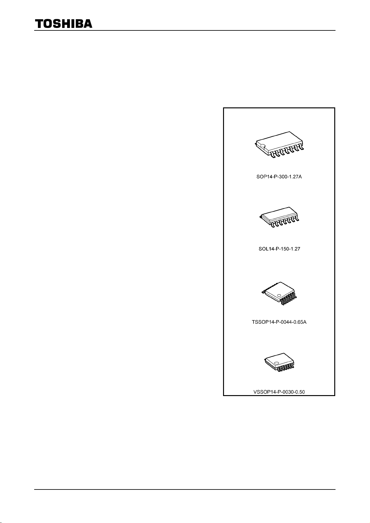
• Available in JEDEC SOP, JEITA SOP, TSSOP and
VSSOP (US)
• Power-down protection provided on all inputs and outputs
• Pin and function compatible with the 74 series
(74AC/VHC/HC/F/ALS/LS etc.) 04 type
Note: The Electrical Characteristics of V
from January 2009 onward.
= 1.65 to 3.6 V
CC
= 5.2 ns (max) (V
pd
= 24 mA (min) (V
OL
= 3.0 to 3.6 V)
CC
= 3.0 V)
CC
=1.8±0.15V is only applicable for products which manufactured
CC
Note: xxxFN (JEDEC SOP) is not available in
Japan.
TC74LCX04F
TC74LCX04FN
TC74LCX04FT
TC74LCX04FK
Weight
SOP14-P-300-1.27A : 0.18 g (typ.)
SOL14-P-150-1.27 : 0.12 g (typ.)
TSSOP14-P-0044-0.65A : 0.06 g (typ.)
VSSOP14-P-0030-0.50 : 0.02 g (typ.)
1
2010-01-31
TC74LCX04F/FN/FT/FK
Pin Assignment
(top view)
IEC Logic Symbol
V
1A 1
1Y
2A
2Y
3A
3Y
GND
2
3
4
5
6
7
14
13
12
11
10
9
8
CC
6A
6Y
5A
5Y
4A
4Y
Truth Table
Inputs Outputs
A Y
L H
H L
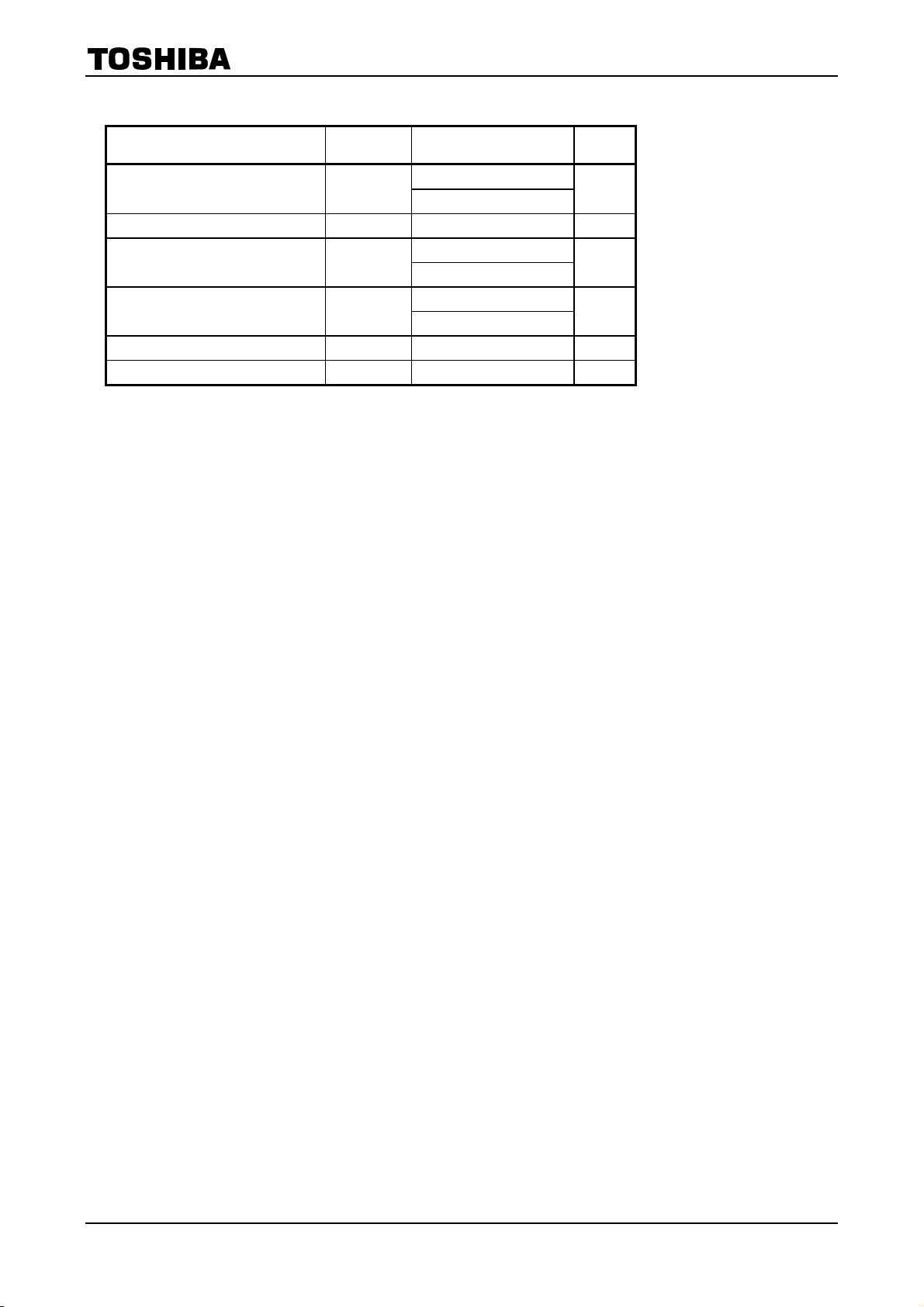
Absolute Maximum Ratings (Note 1)
1A
2A
3A
4A
5A
6A
11
13
1
3
5
9
1
2
4
6
8
10
12
1Y
2Y
3Y
4Y
5Y
6Y
Characteristics Symbol Rating Unit
Power supply voltage V
DC input voltage V
DC output voltage V
Input diode current I
Output diode current I
DC output current I
Power dissipation P
DC VCC/ground current ICC/I
Storage temperature T
CC
IN
OUT
IK
OK
OUT
D
GND
stg
−0.5 to 7.0 (Note 2)
±50 (Note 4) mA
−0.5 to 7.0 V
−0.5 to 7.0 V
−0.5 to VCC + 0.5
(Note 3)
−50 mA
±50 mA
180 mW
±100 mA
−65 to 150 °C
V
Note 1: Exceeding any of the absolute maximum ratings, even briefly, lead to deterioration in IC performance or
even destruction.
Using continuously under heavy loads (e.g. the application of high temperature/current/voltage and the
significant change in temperature, etc.) may cause this product to decrease in the reliability significantly
even if the operating conditions (i.e. operating temperature/current/voltage, etc.) are within the absolute
maximum ratings and the operating ranges.
Please design the appropriate reliability upon reviewing the Toshiba Semiconductor Reliability Handbook
(“Handling Precautions”/“Derating Concept and Methods”) and individual reliability data (i.e. reliability test
report and estimated failure rate, etc).
Note 2: V
Note 3: High or low state. I
Note 4: V
CC
OUT
= 0 V
< GND, V
absolute maximum rating must be observed.
OUT
> VCC
OUT
2
2010-01-31
Operating Ranges (Note 1)
Characteristics Symbol Rating Unit
TC74LCX04F/FN/FT/FK
Power supply voltage V
Input voltage V
Output voltage V
Output current IOH/IOL
Operating temperature T
Input rise and fall time dt/dv 0 to 10 (Note 7) ns/V
CC
IN
OUT
opr
1.5 to 3.6 (Note 2)
0 to 5.5 (Note 3)
0 to VCC (Note 4)
±24 (Note 5)
±12 (Note 6)
1.65 to 3.6
0 to 5.5 V
−40 to 85 °C
V
V
mA
Note 1: The operating ranges must be maintained to ensure the normal operation of the device.
Unused inputs must be tied to either V
or GND.
CC
Note 2: Data retention only
Note 3: V
Note 4: High or low state ( However, it can not exceed I
CC
= 0 V
of absolute maximum ratings. )
OUT
Note 5: VCC = 3.0 to 3.6 V
Note 6: VCC = 2.7 to 3.0 V
Note 7: VIN = 0.8 to 2.0 V, VCC = 3.0 V
3
2010-01-31
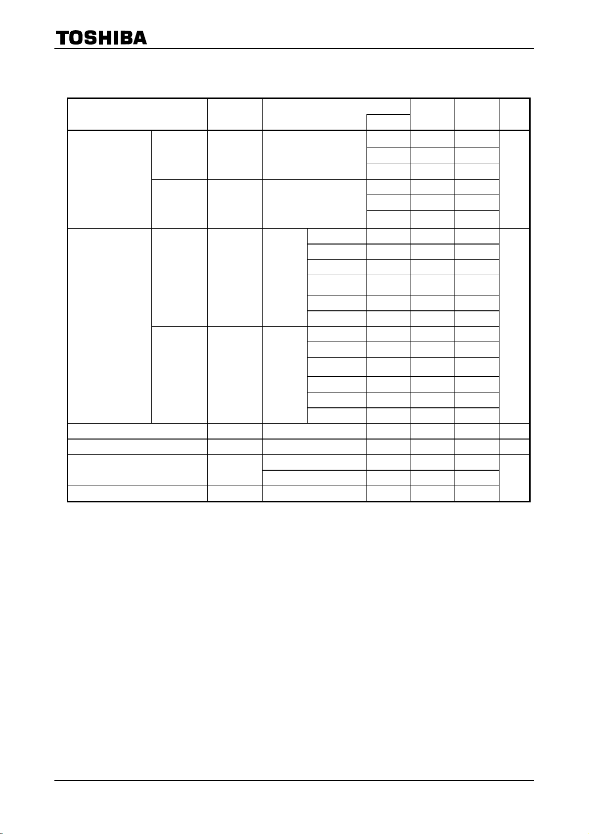
Electrical Characteristics
TC74LCX04F/FN/FT/FK
DC Characteristics
Characteristics Symbol Test Condition
Input voltage
Output voltage
Input leakage current I
Power-off leakage current I
Quiescent supply current ICC
Increase in Icc per input ΔICC VIH = VCC − 0.6 V 2.7 to 3.6 ⎯ 500
(Ta = −40 to 85°C)
H-level
L-level V
H-level
L-level VOL VIN = VIH
VIH ⎯
⎯
IL
V
V
OH
IN
VIN/V
OFF
= VIL
IN
VIN = 0 to 5.5 V 1.65 to 3.6 ⎯ ±5.0 μA
= 5.5 V 0 ⎯ 10.0 μA
OUT
VIN = VCC or GND 1.65 to 3.6 ⎯ 10.0
V
= 3.6 to 5.5 V 1.65 to 3.6 ⎯ ±10.0
IN
(V)
V
CC
1.65 to 2.3 VCC×0.9 ⎯
2.3 to 2.7 1.7 ⎯
2.7 to 3.6 2.0 ⎯
1.65 to 2.3 ⎯ VCC×0.1
2.3 to 2.7 ⎯ 0.7
2.7 to 3.6 ⎯ 0.8
IOH = −100 μA 1.65 to 3.6 VCC−0.2 ⎯
IOH = −4 mA 1.65 1.05 ⎯
IOH = −8 mA 2.3 1.7 ⎯
IOH = −12 mA 2.7 2.2 ⎯
IOH = −18 mA 3.0 2.4 ⎯
= −24 mA 3.0 2.2 ⎯
I
OH
IOL = 100 μA 1.65 to 3.6 ⎯ 0.2
IOL = 4 mA 1.65 ⎯ 0.45
IOL = 8 mA 2.3 ⎯ 0.7
IOL = 12 mA 2.7 ⎯ 0.4
IOL = 16 mA 3.0 ⎯ 0.4
= 24 mA 3.0 ⎯ 0.55
I
OL
Min Max Unit
V
V
μA
4
2010-01-31
 Loading...