TC74ACT299P/F
TOSHIBA CMOS Digital Integrated Circuit Silicon Monolithic
TC74ACT299P,TC74ACT299F
8-Bit PIPO Shift Register with Asynchronous Clear
The TC74ACT299 is an advanced high speed CMOS 8-BIT
PIPO SHIFT REGISTER fabricated with silicon gate and
double-layer metal wiring C
It achieves the high speed operation similar to equivalent
Bipolar Schottky TTL while maintaining the CMOS low power
dissipation.
This device may be used as a level converter for interfacing
TLL or NMOS to High Speed CMOS. The inputs are compatible
with TTL, NMOS and CMOS output voltage levels.
It has a four modes (HOLD, SHIFT LEFT, SHIFT RIGHT and
LOAD DATA) controlled by the two selection inputs (S0, S1).
When one or both enable (
outputs are forced to the high-impedance state; however,
sequential operation or clearing of the register is not affected.
All inputs are equipped with protection circuits against static
discharge or transient excess voltage.
2
MOS technology.
1G
, 2G) are high, the eight I/O
Features (Note 1)(Note 2)
• High speed: f
• Low power dissipation: I
• Compatible with TTL outputs: V
VIH = 2.0 V (min)
• Symmetrical output impedance: |I
Capability of driving 50 Ω
transmission lines.
• Balanced propagation delays: t
• Pin and function compatible with 74F299
= 130 MHz (typ.) at VCC = 5 V
max
= 8 μA (max) at Ta = 25°C
CC
= 0.8 V (max)
IL
| = IOL = 24 mA (min)
OH
∼
t
−
pLH
pHL
TC74ACT299P
TC74ACT299F
Weight
DIP20-P-300-2.54A : 1.30 g (typ.)
SOP20-P-300-1.27A : 0.22 g (typ.)
Note 1: Do not apply a signal to any bus terminal when it is in the output mode. Damage may result.
Note 2: All floating (high impedance) bus terminals must have their input levels fixed by means of pull up or pull
down resistors.
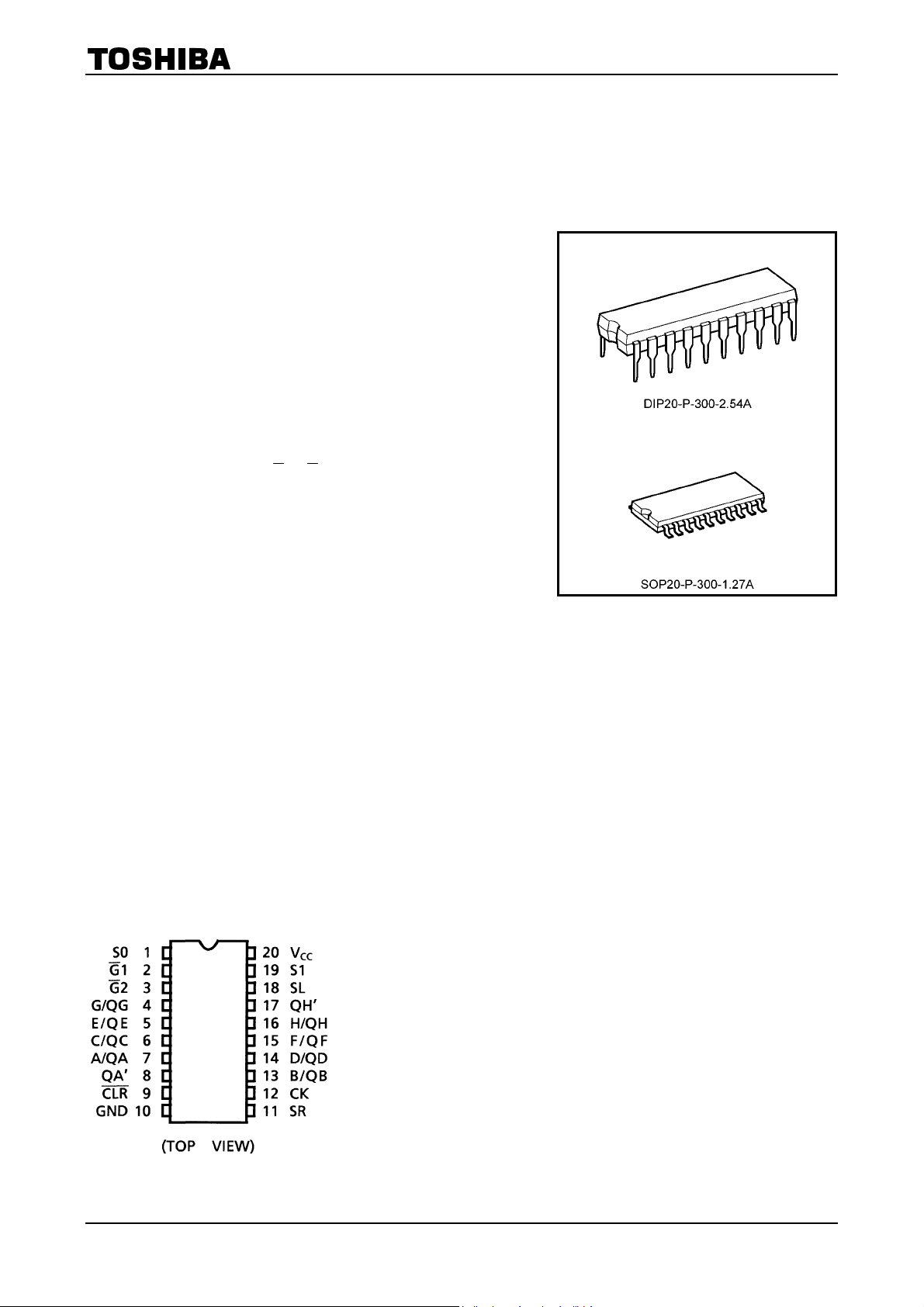
Pin Assignment
1
2007-10-01

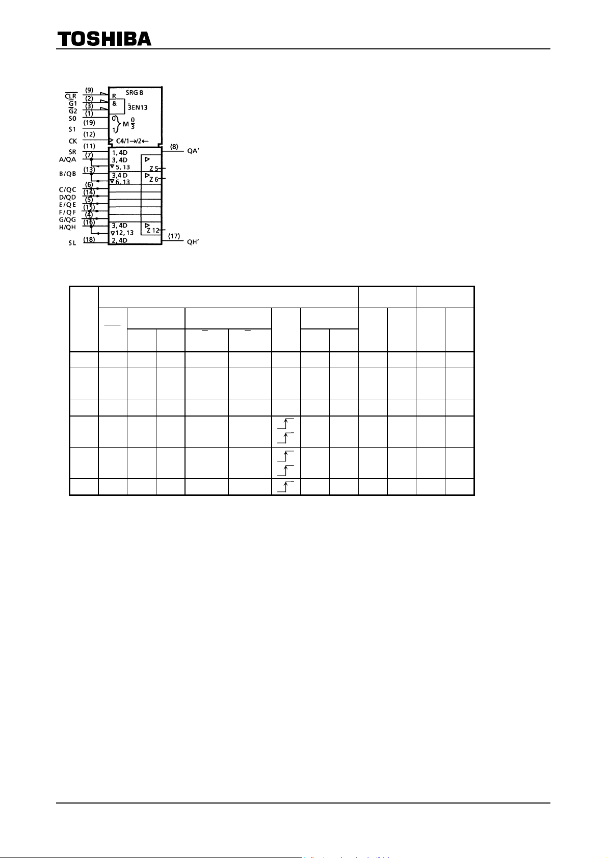
IEC Logic Symbol
Truth Table
TC74ACT299P/F
Inputs
Mode
CLR
Z L H H X X X X X Z Z L L
Clear
Hold H L L L L X X X QA0 QH0 QA0 QH0
Shift H L H L L X H H QGn H QGn
Right H L H L L X L L QGn L QGn
Shift H H L L L H X QBn H QBn H
Left H H L L L L X QBn L QBn L
Load H H H X X X X a h a h
L L X L L X X X L L L L
L X L L L X X X L L L L
Function
Select
S1 S0
Outputs Control Serial
1G
(Note)
(Note)
2G
CK
SL SR
Inputs/
Outputs
A/QA H/QH QA’ QH’
Outputs
Note: When one or both output controls are high, the eight input/output terminals are in the high-impedance state;
however sequential or clearing of the register is not affected.
Z: High impedance
Qn0: The level of Qn before the indicated steady-state input conditions were established.
Qnn: The level of Qn before the most recent active transition indicated by ↓ or ↑.
a, h: The level of the steady-state inputs A, H, respectively.
X: Don’t care
2
2007-10-01

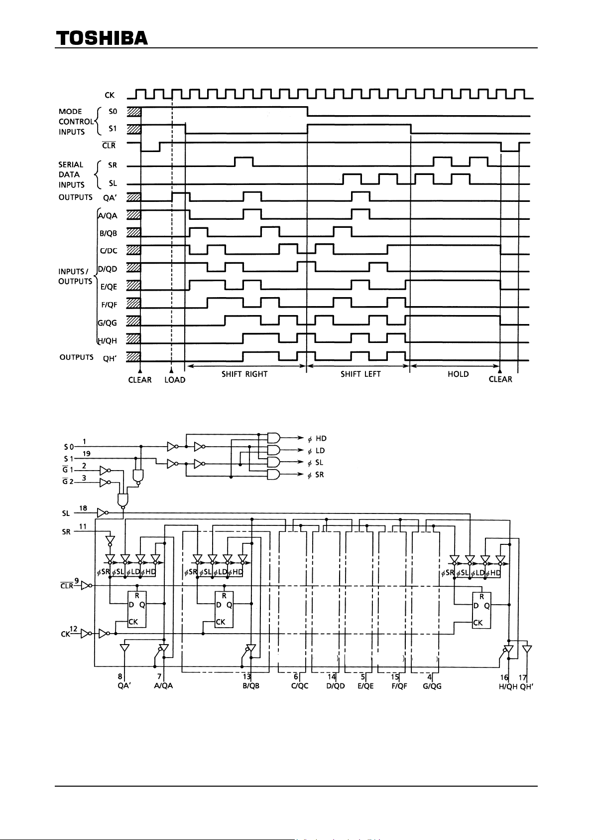
Timing Chart
TC74ACT299P/F
System Diagram
(Note)
(Note) (Note) (Note) (Note)(Note)
Note: Equivalent circuits
3
2007-10-01
 Loading...