

TOSHIBA TC74ACT164P, TC74ACT164F, TC74ACT164FN Technical data
TC74ACT164P/F/FN
TOSHIBA CMOS Digital Integrated Circuit Silicon Monolithic
TC74ACT164P,TC74ACT164F,TC74ACT164FN
8-Bit Shift Register (S-IN, P-OUT)
The TC74ACT164 is an advanced high speed CMOS 8-BIT
SERIAL-IN PARALLEL-OUT SHIFT REGISTER fabricated with
silicon gate and double-layer metal wiring C2MOS technology.
It achieves the high speed operation similar to equivalent
Bipolar Schottky TTL while maintaining the CMOS low power
dissipation.
This device may be used as a level converter for interfacing
TTL or NMOS to High Speed CMOS. The inputs are compatible
with TTL, NMOS and CMOS output voltage levels.
It consists of a serial-in, parallel-out 8-bit shift register with a
CLOCK input and an overriding
Two serial data inputs (A, B) are provided so that one may be
used as a data enable.
All inputs are equipped with protection circuits against static
discharge or transient excess voltage.
Features
CLEAR
input.
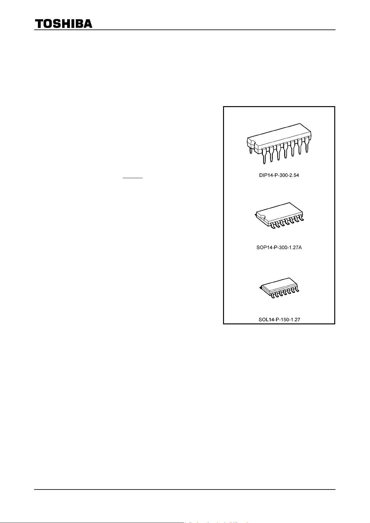
Note: xxxFN (JEDEC SOP) is not available in
Japan.
TC74ACT164P
TC74ACT164F
• High speed: f
• Low power dissipation: I
• Compatible with TTL outputs: V
VIH = 2.0 V (max)
• Symmetrical output impedance: |I
Capability of driving 50 Ω
transmission lines.
• Balanced propagation delays: t
• Pin and function compatible with 74F164
= 200 MHz (typ.) at VCC = 5 V
max
= 8 μA (max) at Ta = 25°C
CC
= 0.8 V (max)
IL
| = IOL = 24 mA (min)
OH
∼
t
−
pLH
pHL
TC74ACT164FN
Weight
DIP14-P-300-2.54 : 0.96 g (typ.)
SOP14-P-300-1.27A : 0.18 g (typ.)
SOL14-P-150-1.27 : 0.12 g (typ.)
1
2007-10-01
TC74ACT164P/F/FN
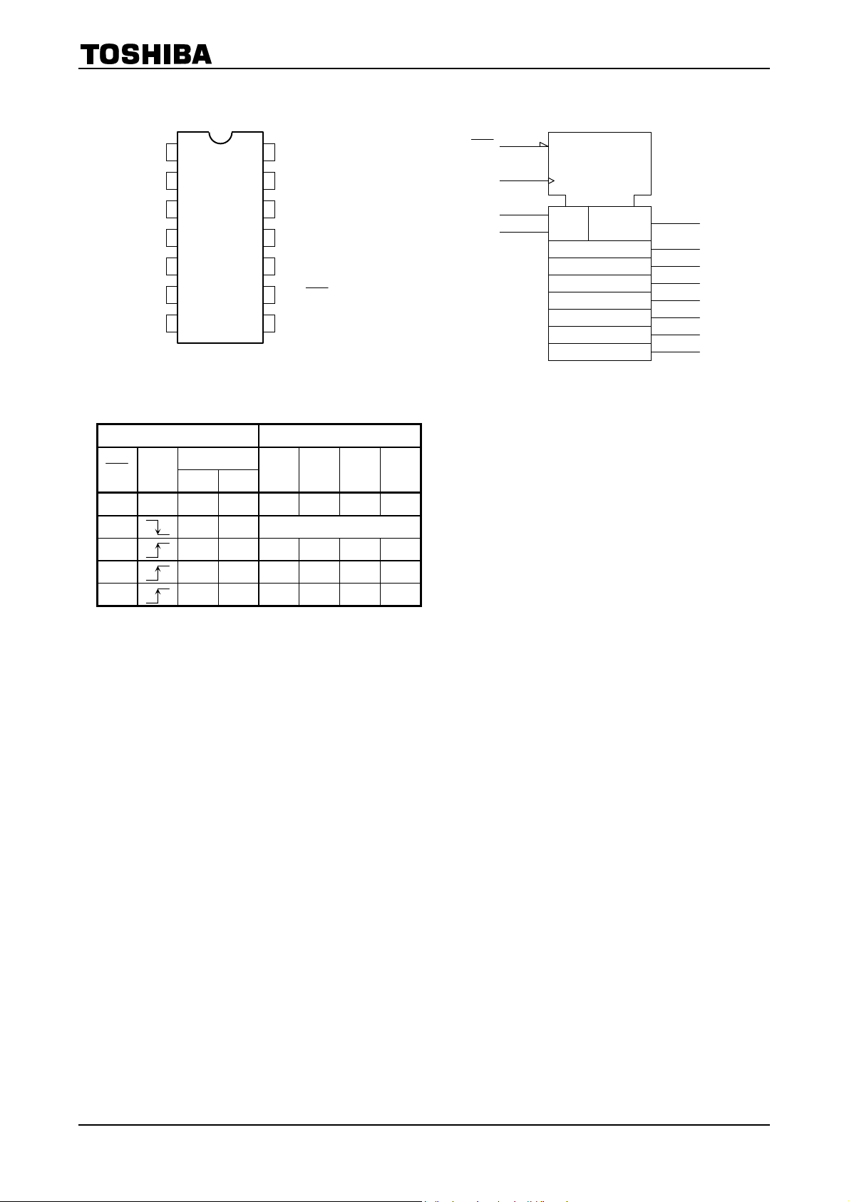
Pin Assignment IEC Logic Symbol
CK
(9)
(8)
R
C1/→
V
A
1
B
2
14
13
CC
QH
CLR
SRG8
QA
QB
QC
QD
GND
3
4
5
6
7
(top view)
12
11
10
9
8
QG
QF
QE
CLR
CK
Truth Table
Inputs Outputs
CLR CK
L X X X L L … L
H X X No change
H L X L QAn … QG
H X L L QAn … QG
H H H H QAn … QG
Serial IN
A B
QA QB … QH
(1)
A
B
n
n
n
(2)
&
1D
(3)
(4)
(5)
(6)
(10)
(11)
(12)
(13)
QA
QB
QC
QD
QE
QF
QG
QH
X : Don’t care
QAn~QGn : The level of QA~QG, respectively, before the most recent positive edge of the clock.
2
2007-10-01
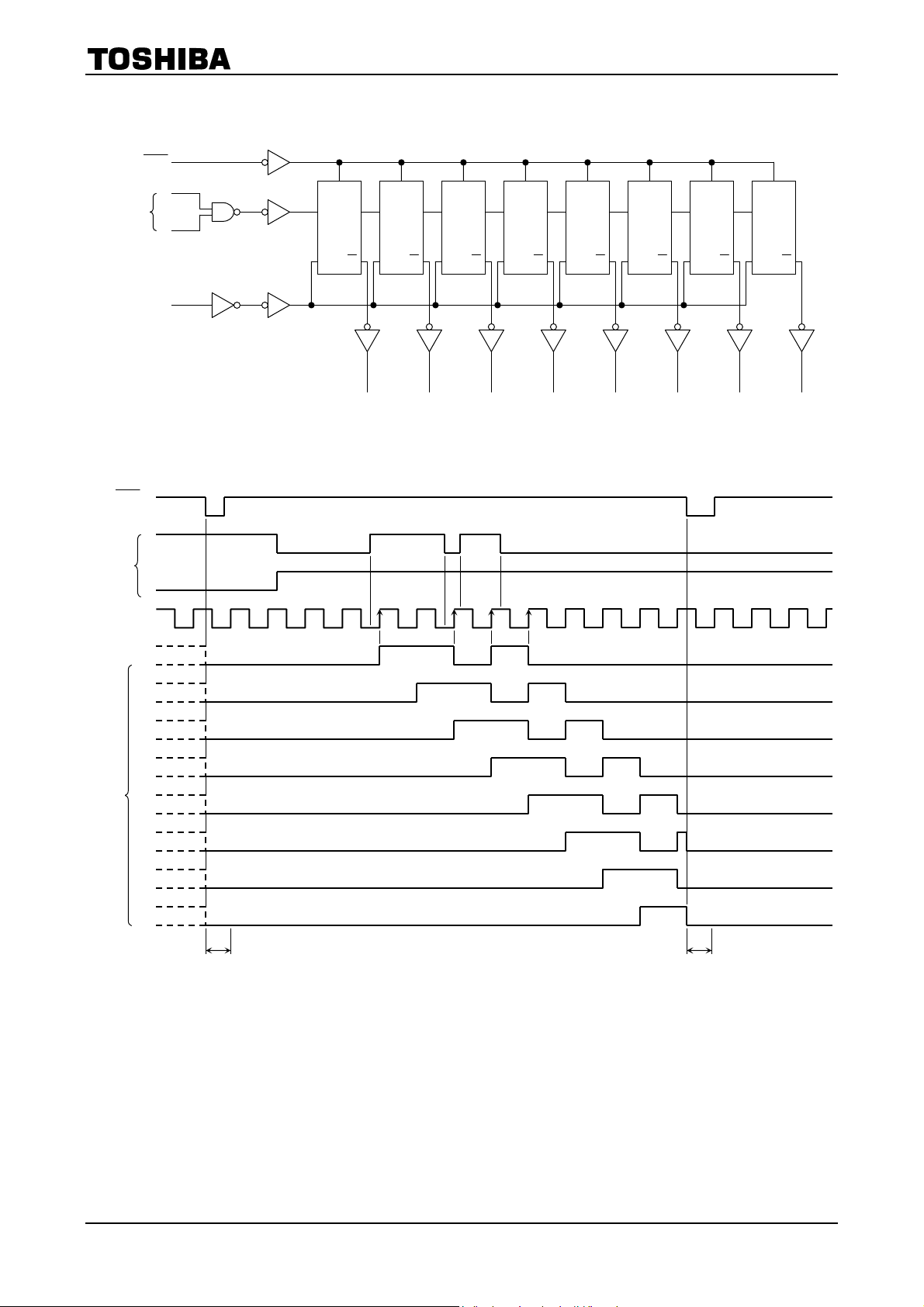
System Diagram
CK
9
1
A
2
B
8
CLR
Serial
inputs
Timing Chart
CLR
TC74ACT164P/F/FN
R
D Q
CK
Q
R
D Q
CK
3 4 5 6 10 11 12 13
QA QB QC QD QG QHQE QF
Q
R
D Q
CK
R
D Q
CK
Q
Q
R
D Q
CK
Q
R
D Q
CK
Q
R
D Q
CK
R
D Q
CK
Q
Q
Serial
inputs
Outputs
A
B
CK
QA
QB
QC
QD
QE
QF
QG
QH
Clear Clear
3
2007-10-01
 Loading...