

www.DataSheet4U.com
DataSheet4U.com
DataSheet4U.com
DataSheet4U.com
DataSheet4U.com
TOSHIBA Bi-CMOS Integrated Circuit Silicon Monolithic
TB6556F/FG
3-Phase Full-Wave Sine-Wave PWM Brushless Motor Controller
Features
• Sine-wave PWM control
• Built-in triangular-wave generator
(carrier cycle = f
• Built-in lead angle control function (0° to 58° in 32 steps)
External setting/automatic internal setting
• Built-in dead time function (setting 2.6 µs or 3.8 µs)
• Supports bootstrap circuit
• Overcurrent protection signal input pin
• Built-in regulator (V
• Operating supply voltage range: V
/252 (Hz))
osc
refout
= 5 V (typ.), 30 mA (max))
= 6 V to 10 V
CC
Weight: 0.33 g (typ.)
TB6556F/FG
TB6556FG:
TB6556FG is a Pb-free product.
The following conditions apply to solderability:
*Solderability
1. Use of Sn-63Pb solder bath
*solder bath temperature = 230˚C
*dipping time = 5 seconds
*number of times = once
*use of R-type flux
2. Use of Sn-3.0Ag-0.5Cu solder bath
*solder bath temperature = 245˚C
*dipping time = 5 seconds
*the number of times = once
*use of R-type flux
1
2005-01-19
www.DataSheet4U.com
DataSheet4U.com
DataSheet4U.com
DataSheet4U.com
DataSheet4U.com
DataSheet4U.com
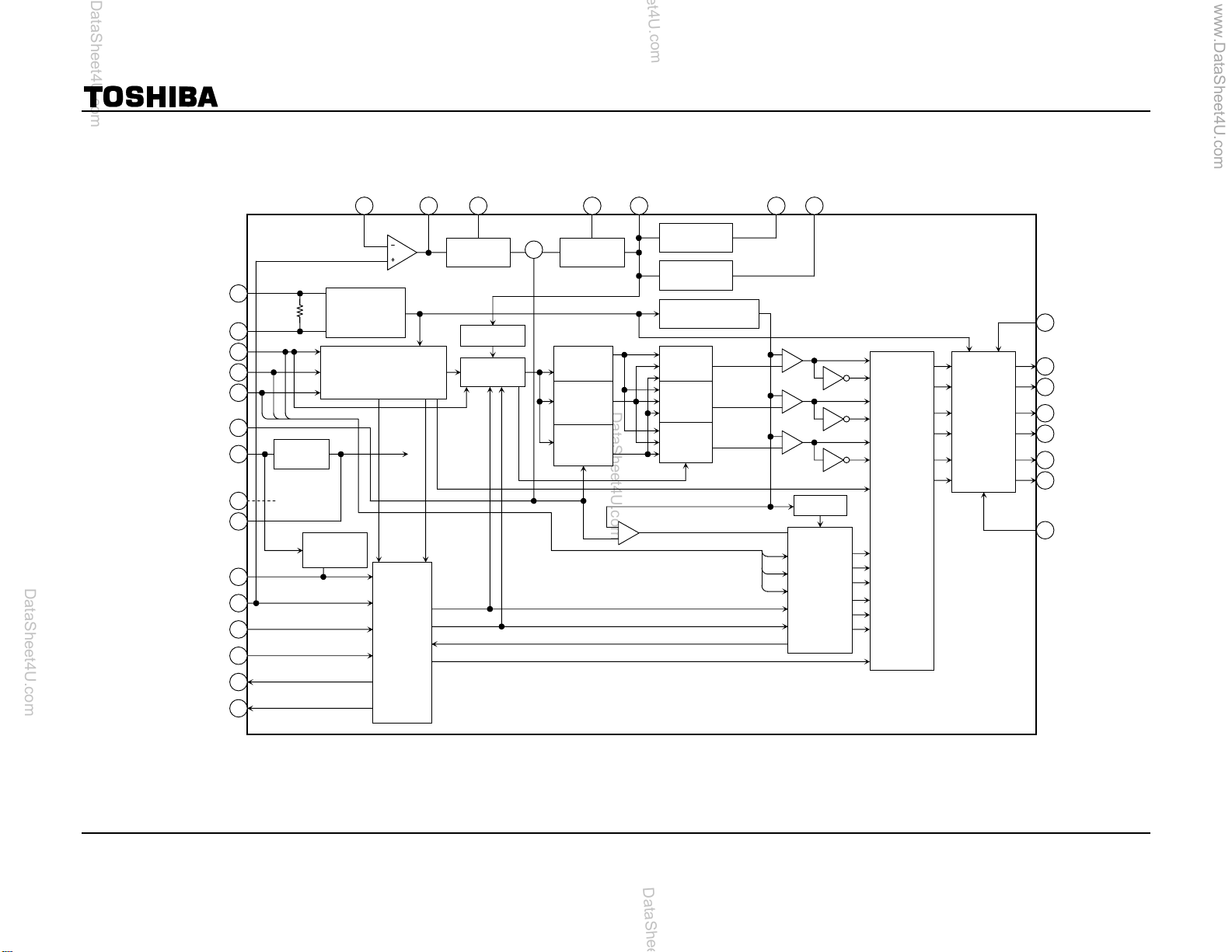
Block Diagram
+
G
G
in
out
PH
2524 26 27
LPF
LA
28
UL
LL
30 29
TB6556F/FG
X
X
out
HU
HV
HW
V
V
CC
GND
V
refout
RES
I
CW/CCW
SS
FG
EV
Peak hold Filter
14
in
15
21
20
19
2
e
Regulator
1
13
23
11
3
dc
18
22
17
16
System clock
generator
Position detector
Power-on
reset
Internal
reference
voltage
FG
Protection
&
reset
Phase
matching
Rotating
direction
ST/SP
CW/CCW
ERR
GB
5-bit AD
Counter
Output
waveform
generator
Upper limit
Lower limit
6-bit triangular
wave generator
Data
select
Comparator
Phase U
Phase V
Phase W
PWM
HU
HV
HW
Comparator
Comparator
Comparator
120/180
Charger
120°-
turn-on
matrix
Switching
120°/180°
and
gate block
protection
on/off
Setting
dead
time
10
12
Td
U
9
X
6
V
8
Y
5
W
7
Z
4
OS
2
2005-01-19
www.DataSheet4U.com
DataSheet4U.com
DataSheet4U.com
DataSheet4U.com
DataSheet4U.com
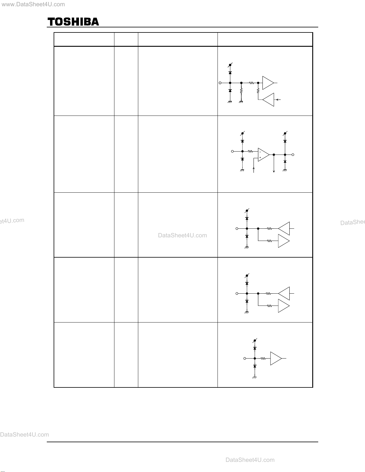
Pin Description
∼
Pin No. Symbol Description Remarks
TB6556F/FG
21 HU Positional signal input pin U
20 HV Positional signal input pin V
19 HW Positional signal input pin W
18 CW/CCW
11 RES Reset-signal-input pin
2 Ve Volt age command signal With built-in pull-down resistor
24 Gin
25 G
26 PH Peak hold
27 LPF RC low-pass filter Connect the low-pass filter capacitor (built-in 100 kΩ resistor)
28 LA
29 LL Lower limit for LA Set lower limit for LA (LL = 0 V to 5.0 V)
30 UL Upper limit for LA Set upper limit for LA (UL = 0 V to 5.0 V)
12 OS
3 Idc
14 Xin Inputs clock signal
15 X
23 V
17 FG FG signal output pin Outputs 3 PPR of positional signal
16 REV
9 U Outputs turn-on signal
8 V Outputs turn-on signal
7 W Outputs turn-on signal
6 X Outputs turn-on signal
5 Y Outputs turn-on signal
4 Z Outputs turn-on signal
1 VCC Power supply voltage pin VCC = 6 to 10 V
10 Td Inputs setting dead time L: 3.8 µs, H or OPEN : 1.9 µs
22 SS 120°/180° select signal L: 120° tu rn- o n m o de, H o r OPEN: 1 80° turn-on mode
13 GND Ground pin ⎯
refout
Rotation direction signal input
pin
Gain setting I
out
Lead angle setting signal
input pin
Inputs output logic select
signal
Inputs overcurrent protection
signal
Outputs clock signal
out
Outputs reference voltage
signal
Reverse rotation detection
signal
When positional signal is HHH or LLL, gate block protection operates.
With built-in pull-up resistor, built-in digital filter (
L: Forward
H: Reverse
L: Reset (output is non-active)
operation/halt operation, also used for gate protection,
built-in pull-up resistor
signal level at a gain that optimizes the LA
dc
Connect the peak-hold capacitor and discharge resistor to GND, parallel
to each other
Sets 0° to 58° in 32 steps
L: Active LOW
H: Active HIGH
Inputs DC link current.
Reference voltage: 0.5 V
With built-in filter (
With built-in feedback resistor
5 V (typ.), 30 mA (max)
Detects reverse rotation.
Select active HIGH or active LOW using the output logic select pin.
1 µs), built-in digital filter (
∼
−
∼
−
1 µs)
500 ns)
3
2005-01-19
www.DataSheet4U.com
DataSheet4U.com
DataSheet4U.com
DataSheet4U.com
DataSheet4U.com
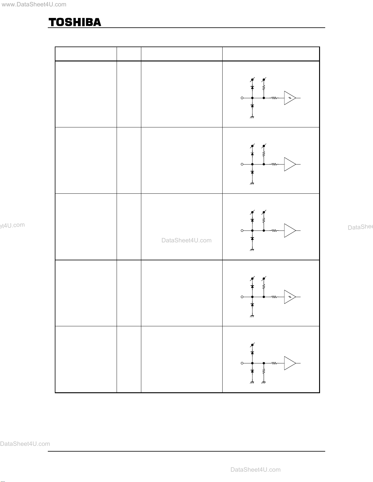
Input/Output Equivalent Ci rcuits
Pin Description Symbol Input/Output Signal Input/Output Internal Circuit
Digital
Positional signal input pin U
Positional signal input pin V
Positional signal input pin W
Forward/reverse switching
input pin
L: Forward (CW)
H: Reverse (CCW)
CW/CCW
With Schmitt trigger
HU
Hysteresis 300 mV (typ.)
HV
Digital filter: 500 ns (typ.)
HW
L: 0.8 V (max)
H: V
Digital
L: 0.8 V (max)
H: V
− 1 V (min)
refout
− 1 V (min)
refout
TB6556F/FG
V
V
refout
refout
200 kΩ
2.0 kΩ
V
V
refout
refout
100 kΩ
2.0 kΩ
V
V
refout
refout
Reset input
L: Stops operation (reset)
H: Operates
120°/180° select si g nal
L: 120° turn-on mode
H: 180° turn-on mode
(OPEN)
Voltage command signal
1.0 V < Ve ≤ 2.1 V
Refresh operation
(X, Y, Z pins: ON duty of
8%)
RES
SS
V
e
Digital
L: 0.8 V (max)
H: V
Digital
With Schmitt trigger
Hysteresis: 300 mV (typ.)
L: 0.8 V (max)
H: V
Analog
Input voltage range 0 to 5.4 V
Input voltage of 5.4 V or higher is
clipped to 5.4 V.
refout
refout
− 1 V (min)
− 1 V (min)
100 kΩ
2.0 kΩ
V
V
refout
refout
200 kΩ
2.0 kΩ
V
CC
100 Ω
150 kΩ
4
2005-01-19
www.DataSheet4U.com
DataSheet4U.com
DataSheet4U.com
DataSheet4U.com
DataSheet4U.com
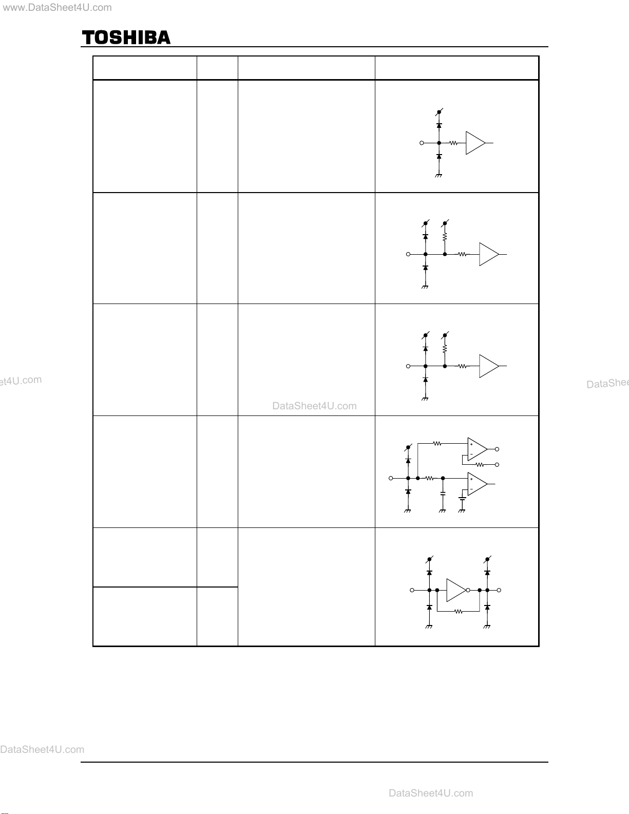
TB6556F/FG
A
Pin Description Symbol Input/Output Signal Input/Output Internal Circuit
Lead angle setting signal
input pin
0 V: 0°
5 V: 58°
(5-bit AD)
Gain setting signal input
(LA setting)
Peak hold
(LA setting)
Gin
G
PH
When LA is fixed externally, connect
LL to GND and UL to V
input the setting voltage to the LA pin.
Input voltage range: 0 V to 5.0 V
(V
)
LA
out
refout
Input voltage of V
clipped to V
When LA is fixed automatically, open
the LA pin. In this state, the LA pin is
used only for confirmation of LA width.
Non-inverted amplifier
25 dB (max)
output voltage
G
out
LOW: GND
HIGH: V
CC
Connect the peak-hold capacitor and
discharge resistor to GND, parallel to
each other.
100 kΩ/0.1µF recommended
.
refout
− 1.7 V
refout
, and then
refout
or higher is
V
V
CC
CC
100 Ω
200 kΩ
200 kΩ
utomatic LA
circuit
CC
G
in
100 Ω
Idc
VCC V
To peak
hold circuit
G
out
V
CC
100 Ω
100 Ω
Low-pass filter
(LA setting)
Lower limit for LA LL
LPF
Connect the low-pass filter capacitor
(built-in 100 kΩ resistor)
0.1µF recommended
Clip lower limit for LA
LL = 0 V to 5.0 V
When LL > UL, LA is fixed at LL value.
V
CC
100 kΩ
100 Ω
VCC
100 Ω
5
2005-01-19
www.DataSheet4U.com
DataSheet4U.com
DataSheet4U.com
DataSheet4U.com
DataSheet4U.com
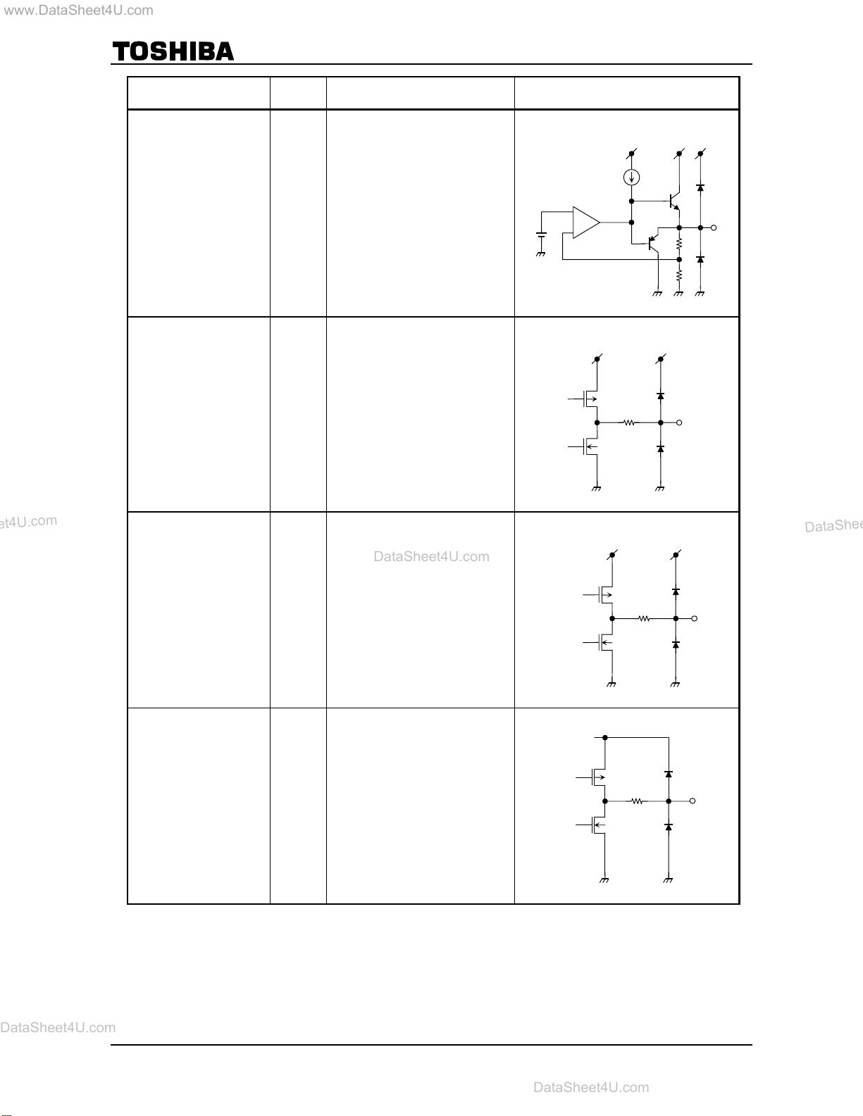
TB6556F/FG
Pin Description Symbol Input/Output Signal Input/Output Internal Circuit
VCC
Upper limit for LA UL
Setting dead time input pin
L: 3.8 µs
H or OPEN: 1.9 µs
Output logic select signal
input pin
L: Active LOW
H: Active HIGH
Overcurrent protection
signal input pin
Clock signal input pin Xin
Td
OS
I
dc
Clip upper limit for LA
UL = 0 V to 5.0 V
When LL > UL, LA is fixed at LL value.
Digital
L: 0.8 V (max)
H: V
Digital
L: 0.8 V (max)
H: V
Analog
Digital filter: 1 µs (typ.)
Gate pr otected at 0.5 V or higher
(released at carrier cycle)
refout
refout
− 1 V (min)
− 1 V (min)
100 Ω
V
V
refout
refout
100 kΩ
2 kΩ
V
V
refout
refout
100 kΩ
2 kΩ
100 Ω
V
CC
200 kΩ
5 pF
0.5 V
V
V
refout
G
out
Gin
Comparator
refout
Clock signal output pin X
Operat ing range
2 MHz to 8 MHz (crystal oscillation)
out
X
in
360 kΩ
6
X
out
2005-01-19
www.DataSheet4U.com
DataSheet4U.com
DataSheet4U.com
DataSheet4U.com
DataSheet4U.com
TB6556F/FG
Pin Description Symbol Input/Output Signal Input/Output Internal Circuit
VCC VCC
V
CC
Reference voltage signal
output pin
Reverse-rotation-detection
signal output pin
FG signal output pin FG
V
refout
REV
5 ± 0.5 V (max 30 mA)
Digital
Push-pull output: ± 1 mA (max)
Digital
Push-pull output: ± 1 mA (max)
V
refout
V
V
refout
V
refout
100 Ω
refout
100 Ω
Turn-on signal output pin U
Turn-on signal output pin V
Turn-on signal output pin W
Turn-on signal output pin X
Turn-on signal output pin Y
Turn-on signal output pin Z
U
Analog
V
W
Push-pull output: ± 2 mA (max)
X
Y
L: 0.78 V (max)
Z
H: V
− 0.78 V (min)
refout
V
refout
100 Ω
7
2005-01-19

www.DataSheet4U.com
DataSheet4U.com
DataSheet4U.com
DataSheet4U.com
DataSheet4U.com
TB6556F/FG
Maximum Ratings
Characteristics Symbol Rating Unit
Supply voltage VCC 12 V
Input voltage
Turn-on signal output current I
Power dissipation PD 1.50 (Note 3) W
Operating temperature T
Storage temperature T
Note 1: V
Note 2: V
in (1)
in (2)
(Ta = 25°C)
pin: Ve, LA, Gin, G
pin: HU, HV, HW, CW/CCW, RES, OS, Idc, Td, SS
V
−0.3~VCC (Note 1)
in (1)
V
−0.3~V
in (2)
2 mA
OUT
−30~115 (Note 4) °C
opr
−50~150 °C
stg
, PH, LPF, LL, UL
out
+ 0.3 (Note 2)
refout
V
Note 3: When mounted on PCB (universal 50 × 50 × 1.6 mm, Cu 30%)
Note 4: Operating temperature r ange is deter m i ned by the PD − Ta characteristic.
Recommended Operati ng Co ndi tions
Characteristics Symbol Min Typ. Max Unit
Supply voltage VCC 6 7 10 V
Crystal oscillation frequency Xin 2 4 8 MHz
(Ta = 25°C)
2.0
1.5
(W)
D
1.0
P
– Ta
D
(1) When mounted on PCB
(2) IC only
(1)
Universal
50 × 50 × 1.6 mm
R
= 110°C/W
th (j-a)
Power dissipation P
0.5
(2)
0
0
50 100 150 200
Ambient temperature Ta (°C)
8
2005-01-19

www.DataSheet4U.com
DataSheet4U.com
DataSheet4U.com
DataSheet4U.com
DataSheet4U.com
TB6556F/FG
Electrical Characteristics
Characteristics Symbol
(Ta = 25°C, VCC = 7 V)
Test
Circuit
Supply current ICC ⎯ V
I
-1 Vin = 5 V LA ⎯ 25 50
in (1)
I
-2 Vin = 5 V Ve ⎯ 35 70
Input current
in (1)
I
-1 Vin = 0 V HU, HV, HW, SS −50 −25 ⎯
in (2)
I
-2
in (2)
HIGH
V
in
⎯
⎯ HU, HV, HW, CW/CCW, RES, OS, Td, SS
LOW
Input voltage
H PWM Duty 100% 5.1 5.4 5.7
V
e
⎯
M Refresh → Start motor operation 1.8 2.1 2.4
L
Input hysteresis
voltage
Input delay time
Output voltage
Output leakage
current
Output off-time by
upper/lower transistor
(Note 6)
V
⎯ HU, HV, HW, SS (Note 5) ⎯ 0.3 ⎯ V
H
VDT HU, HV, HW Xin = 4.19 MHz ⎯ 0.5 ⎯
V
DC
V
OUT (H)-1
V
OUT (L)-1
V
REV (H)
V
REV (L)
V
FG (H)
V
FG (L)
V
refout
I
L (H)
I
L (L)
T
OFF (H)
⎯
I
I
I
⎯
I
I
I
V
⎯
⎯
T
OFF (L)
= open ⎯ 5 8 mA
refout
Vin = 0 V CW/CCW, OS, Td, RES −100 −50 ⎯
Turned-off → Refresh 0.7 1.0 1.3
Idc Xin = 4.19 MHz ⎯ 1.0 ⎯
= 2 mA U, V, W, X, Y, Z
OUT
= −2 mA U, V, W, X, Y, Z ⎯ 0.3 0.78
OUT
= 1 mA REV
OUT
= −1 mA REV ⎯ 0.2 1.0
OUT
= 1 mA FG
OUT
= −1 mA FG ⎯ 0.2 1.0
OUT
I
= 30 mA V
OUT
= 0 V U, V, W, X, Y, Z ⎯ 0 10
OUT
V
= 3.5 V U, V, W, X, Y, Z ⎯ 0 10
OUT
Td = HIGH or OPEN, X
I
= ± 2 mA, OS = HIGH/LOW
OUT
Td = LOW, X
I
= ± 2 mA, OS = HIGH/LOW
OUT
Test Condition Min Typ. Max Unit
V
= 4.19 MHz,
in
refout
− 1
V
refout
− 0.78
V
refout
− 1.0
V
refout
− 1.0
4.5 5.0 5.5
refout
= 4.19 MHz,
in
1.5 1.9 ⎯
3.0 3.8 ⎯
⎯ V
refout
⎯ ⎯ 0.8
V
refout
− 0.3
V
refout
− 0.2
V
refout
− 0.2
⎯
⎯
⎯
µA
V
V
µs
V
µA
µs
Overcurrent detection Vdc ⎯ Idc 0.46 0.5 0.54 V
LA gain setting amp
LA limit setting
difference
LA peak hold output
current
Lead angle correction
G
OUT
AMP
OFS
∆L LL = 0.7 V −20 ⎯ 20
∆U
PH
OUT
T
LA (0)
T
LA (2.5)
T
LA (5)
⎯
⎯
⎯ PH output current ⎯ ⎯ 5 mA
⎯ LA = 0 V or OPEN, Hall IN = 100 Hz ⎯ 0 ⎯
⎯ LA = 2.5 V, Hall IN = 100 Hz 27.5 32 34.5
⎯ LA = 5 V, Hall IN = 100 Hz 53.5 59 62.5
output current 5 ⎯ ⎯ mA
OUT
GIN, G
11 kΩ/1 kΩ ⎯ −40 ⎯ mV
OUT
UL = 2.0 V −20 ⎯ 20
mV
°
AMP
VCC (H) ⎯ Output start operation point 4.2 4.5 4.8
VCC monitor
VCC (L) ⎯ No output operation point 3.7 4.0 4.3
V
⎯ Input hysteresis width ⎯ 0.5 ⎯
H
V
Note 5: Toshiba does not implement test i ng befor e shi ppi ng.
9
2005-01-19

www.DataSheet4U.com
DataSheet4U.com
DataSheet4U.com
DataSheet4U.com
DataSheet4U.com
TB6556F/FG
Note 6: T
OFF
OS = HIGH
OS = LOW
Turn-on signal (U, V, W)
Turn-on signal (X, Y, Z)
Turn-on signal (U, V, W)
Turn-on signal (X, Y, Z)
0.78 V
0.78 V 0.78 V
T
OFF
V
refout
T
OFF
V
− 0.78 V V
refout
− 0.78 V
refout
T
OFF
V
T
OFF
− 0.78 V
0.78 V
refout
− 0.78 V
10
2005-01-19

www.DataSheet4U.com
DataSheet4U.com
DataSheet4U.com
DataSheet4U.com
DataSheet4U.com
TB6556F/FG
<
<
<
Functional Description
1. Basic operation
The motor is driven by the square-wave turn-on signal based on a positional signal. When the positional
signal reaches number of rotations f = 5 Hz or higher, the rotor position is estimated according to the
positional signal and a modulation wave is generated. The modulation wave and the triangular wave are
compared; then the sine-wave PWM signal is generated and the motor is driven.
From start to 5 Hz: When driven by square wave (120° turn-on) f = f
5 Hz~: When driven by sine-wave PWM (180° turn-on); when f
osc
2. Select drive function
This function can select drive mode.
SS pin
HIGH or OPEN = Sine-wave PWM drive (180° turn-on mode)
LOW = Square-wave drive (120° turn-on mode)
Note: If the position sens ing signal is f = 5 Hz or lower, t he driver is 120° turn-on mode even when SS =
HIGH.
3. Ve voltage command signal function and function to stabilize bootstrap voltage
(1) When the voltage command signal is input at V
Turns off output (gate protection)
(2) When the voltage command signal is input at 1.0 V
Turns on the lower transistor at the regular (carrier) cycle. (ON duty is approx. 8%.)
(3) When the voltage command signal is input at Ve
During sin-wave drive, outputs drive signal as it is. During square-drive, forcibly turns on the lower
transistor at regular (carrier) cycle. (ON duty is approx. 8%)
Note: At startup, turn the l ower tr ansis tor on for a fixed tim e with 1.0 V
transistor gate power supply.
PWM Duty
1.0 V:
e
> 2.1 V:
< Ve
2.1 V:
/(212 × 32 × 6)
osc
= 4 MHz, approx. 5 Hz
< Ve
2.1 V to charge the upper
100%
(1) (2) (3)
2.1 V1.0 V 5.4 V V
e
4. Dead time function: upper/lower transistor output off-time
When the motor is driven by sine-wave PWM, dead time is digitally generated in the IC to prevent a
short circuit caused by the simultaneous turning on of upper and lower external power devices. When a
square wave is generated in full-duty cycle mode, the dead time function is turned on to prevent a short
circuit.
Td Pin Internal Counter T
HIGH or OPEN 8/f
LOW 16/f
1.9 µs
osc
3.8 µs
osc
T
values above are obtained when fosc = 4.19 MHz.
OFF
f
= reference clock (crystal oscillation)
osc
OFF
11
2005-01-19

www.DataSheet4U.com
DataSheet4U.com
DataSheet4U.com
DataSheet4U.com
DataSheet4U.com
5. Correcting the lead angle
The lead angle can be corrected in the turn-on signal range from 0 to 58° in relation to the induced
voltage.
Analog input from LA pin (0 V to 5 V divided by 32):
0 V
= 0°
5 V
= 58° (when more than 5 V is input, 58°)
6. Setting the carrier frequency
This function sets the triangular wave cycle (carrier cycle) necessary for generating the PWM signal.
(The triangular wave is used for forcibly turning on the lower transistor when the motor is driven by
square wave.)
Carrier cycle
= f
/252 (Hz) f
osc
= reference clock (crystal oscillation)
osc
7. Switching the output of the turn-on signal
This function switches the output of the turn-on signal between HIGH and LOW.
Pin OS:
HIGH
= active HIGH
LOW
= active LOW
8. Outputting the reverse rotation detection signal
This function detects the motor rotation direction every electrical angle of 360°. (The output is HIGH
immediately after reset.)
The REV terminal increases with a 180° turn-on mode during LOW.
TB6556F/FG
CW/CCW Pin Actual Motor Rotating Direction REV Pin
LOW (CW)
HIGH (CCW)
9. Protecting input pin
1. Overcurrent protection (Pin I
When the DC-link-current exceeds the internal reference voltage, performs gate block protection.
Overcurrent protection is released for each carrier frequency.
Reference voltage
2. Gate protection (Pin RES)
Output is turned off when the input signal is LOW, restarted when the input signal is HIGH.
The abnormality is detected externally and the signal input to pin RES.
RES Pin OS Pin
LOW
(When RES
CW (fo rward) LOW
CCW (reverse) HIGH
CW (fo rward) HIGH
CCW (reverse) LOW
)
dc
= 0.5 V (typ.)
Output Turn-on Signal
(U, V, W, X, Y, Z)
LOW HIGH
HIGH LOW
= LOW, bootstrap capacitor charging stops.)
12
2005-01-19

www.DataSheet4U.com
DataSheet4U.com
DataSheet4U.com
DataSheet4U.com
DataSheet4U.com
TB6556F/FG
3. Internal protection
• Positional signal abnormality protection
Output is turned off when the positional signal is HHH or LLL; otherwise, it is restarted.
• Low power supply voltage protection (V
For power supply on/off outside the operating voltage range, the turn-on signal output is kept at
high impedance outside the operating voltage range to prevent damage caused by power device
short circuits.
However, if the voltage level is supplied from the V
4.9 V is applied, low power supply voltage protection does not operate.
Power supply
voltage
Turn-on signal
4.5 V (typ.) 4.0 V (typ.)
monitor)
CC
pin, this function is restricted, e.g., when Ve >
e
V
CC
GND
V
M
Output at high impedance
Output at high impedance Output
13
2005-01-19

www.DataSheet4U.com
DataSheet4U.com
DataSheet4U.com
DataSheet4U.com
DataSheet4U.com
TB6556F/FG
Operation Flow
Positional signal
(Hall IC)
Voltage
instruction
Oscillator
System clock
generator
Position
detector
Phase matching
(Note)
92%
Phase U
Counter
Phase V
Phase
W
Driven by square wave
Sine-wave pattern
(modulation signal)
Triangular wave
(carrier frequency)
U
X
V
Y
Comparator
W
Z
Output ON duty (U, V, W)
2.1 V (typ.)
Voltage comma nd sign al Ve
5.0 V (typ.)
Note: O utput ON t i m e is decreased by the dead time
(carrier frequency
× 92% − T
× 2)
d
100%
Driven by sine wave
Modulation ratio (modulation signal)
0
Voltage comma nd sign al Ve
2.1 V (typ.)
14
5.4 V (typ.)
2005-01-19

www.DataSheet4U.com
DataSheet4U.com
DataSheet4U.com
DataSheet4U.com
DataSheet4U.com
TB6556F/FG
The modulation waveform is generated using Hall signals. The modulation waveform is then compared
with the triangular wave and a sine-wave PWM signal is generated.
The time (electrical degrees: 60°) from the rising (or falling) edges of the three Hall signals to the next
falling (or rising) edges is counted. The counted time is used as the data for the next 60° phase of the
modulation waveform.
There are 32 items of data for the 60° phase of the modulation waveform. The time width of one data
item is 1/32 of the time width of the 60° phase of the previous modulation waveform. The modulation
waveform moves forward by the width.
HU
HV
HW
S
U
S
V
Sw
⑥ ① ③
⑤ ②
⑥’ ①’ ②’ ③’
*HU, HV, HW: Hall signals
In the above diagram, the modulation waveform (1)’ data moves forward by the 1/32 time width of the
time (1) from HU:
HW:
↓ to HV: ↑.
↑ to HW: ↓. Similarly, data (2)’ moves forward by the 1/32 time width of the time (2) from
If the next edge does not occur after the 32 data items end, the next 32 data items move forward by the
same time width until the next edge occurs.
*t
*t
32
31
30
6
5
4
3
2
1
S
V
* t = t(1) × 1/32
(1)’
32 data items
The modulation wave is brought into phase with every zero-cross point of the Hall signal.
The modulation wave is reset in synchronization with the rising and falling edges of the Hall signal at
every 60° electrical angle. Thus, when the Hall device is not placed at the correct position or during
acceleration and deceleration, the modulation waveform is not continuous at every reset.
15
2005-01-19

www.DataSheet4U.com
DataSheet4U.com
DataSheet4U.com
DataSheet4U.com
DataSheet4U.com
Timing Charts
H
Hall signal
(input)
u
H
v
H
w
TB6556F/FG
FG signal
(output)
Turn-on signal
when driven
by square wave
(output)
Modulation
wave f or m whe n
driven by sine wave
(insi d e of IC)
FG
U
V
W
X
Y
Z
S
S
S
Hall signal
(input)
Hu
H
H
u
v
w
Forward
v
w
FG signal
(output)
Turn-on signal
when driven
by square wave
(output)
Modulation
wave f or m whe n
driven by sine wave
(inside the IC)
FG
U
V
W
X
Y
Z
S
S
S
u
v
w
Reverse
16
2005-01-19

www.DataSheet4U.com
DataSheet4U.com
DataSheet4U.com
DataSheet4U.com
DataSheet4U.com
TB6556F/FG
Operating Waveform When Driven by Square Wave
Hall signal
H
U
HV
H
W
Output waveform
U
X
V
Y
W
(CW/CCW = LOW, OS = HIGH)
Z
Enlarged
waveform
W
Z
T
ONU
T
d
T
ONL
T
d
To stabilize the bootstrap voltage, the lower outputs (X, Y, and Z) are always turned on at the carrier cycle
even during off time. At that time, the upper outputs (U, V, and W) are assigned dead time and turned off
at the timing when the lower outputs are turned on. (T
Carrier cycle = f
T
= carrier cycle × 8% (s) (Uniformity)
ONL
/252 (Hz) Dead time: Td = 16/f
osc
varies with input Ve.)
d
(s) (In more than Ve = 5.0 V)
osc
When the motor is driven by a square wave, acceleration or deceleration is determined by voltage V
motor accelerates or decelerates according to the ON duty of T
. (See the diagram of output ON duty on
ONU
page 14.)
Note: At st artup, the motor is driven by a square wave when the Hall signals are 5 Hz or lower (f
the motor is rotating in the reverse direction to that of the TB6556F/FG controlling it (REV
= 4 MHz) and
osc
= HIGH).
. The
e
17
2005-01-19

www.DataSheet4U.com
DataSheet4U.com
DataSheet4U.com
DataSheet4U.com
DataSheet4U.com
TB6556F/FG
Operating Waveform When Driven by Sine- Wave PWM
Generation inside of IC
Phase U
Phase V
Phase W
Output waveform
U
X
V
Y
Modulation signal
(CW/CCW = LOW, OS = HIGH)
Triangular wave (carrier frequency)
W
Z
Inter-line voltage
VUV
(U-V)
V
VW
(V-W)
V
WU
(W-U)
When driven by a sine wave, the motor is accelerated or decelerated according to the ON duty of T
the amplitude of the modulation symbol changes according to voltage V
. (See the diagram of the output
e
ON duty on page 14.)
Triangular wave frequency
= carrier frequency = f
/252 (Hz)
osc
Note: At startup, the motor is driven by a sine wave when the Hall signals are 5 Hz or higher (f
motor is rotating in the same direction as the TB6556F/FG controlling it (REV
= LOW).
ONU
= 4 MHz) and the
osc
as
18
2005-01-19

www.DataSheet4U.com
DataSheet4U.com
DataSheet4U.com
DataSheet4U.com
DataSheet4U.com
DataSheet4U.com
Example of Application Circuit
g
X
in
14
15
X
out
21
HU
20
HV
19
HW
22
V
e
V
CC
MCU
6 to 10 V
GND
V
refout
RES
CW/CCW
REV
SS
FG
13
23
11
I
dc
18
17
16
TB6556F/FG
V
G = 1 + (R2/R1)
R1
R2
Gin G
System clock
generator
Position detector
reference
Regulator
1
Power-on
reset
3
Protection
2
PH
out
2524 26 27LA28
+
Internal
voltage
FG
&
reset
Peak hold Filter
5-bit AD
Counter
Phase
matching
Rotating
direction
ST/SP
CW/CCW
ERR
GB
LPF
Output
waveform
generator
Upper limit
Lower limit
Triangular wave
enerator6-bit
Selecting
data
Comparator
refoutVrefout
UL LL
Phase U
Phase V
Phase W
PWM
30 29
Comparator
Comparator
Comparator
120/180
Charger
HU
HV
HW
120°-
turn-on
matrix
Switching
120°/180° &
gate block
protection
on/off
Setting
dead time
Power
Driver
supply
M
10
Td
9
U
6
X
8
V
5
Y
7
W
4
Z
12
OS
Pre-driver
(charge
pump)
(Note 1)
Note 2: Connect GND to signal ground on the application circuit.
Note 3: The device may be damaged by short circuits between outputs or between output and supply or ground. Peripheral parts may also be damaged by overvoltage and overcurrent. Design the output lines, V
lines to ensure that no short circuits occur.
Be careful also not to insert the IC in the wrong direction since this may destroy the IC.
Note 1: Connect to ground as necessary to prevent IC malfunction due to noise.
(Note 1)
Hall IC signal
CC
2005-01-19 19
and GND

www.DataSheet4U.com
DataSheet4U.com
DataSheet4U.com
DataSheet4U.com
DataSheet4U.com
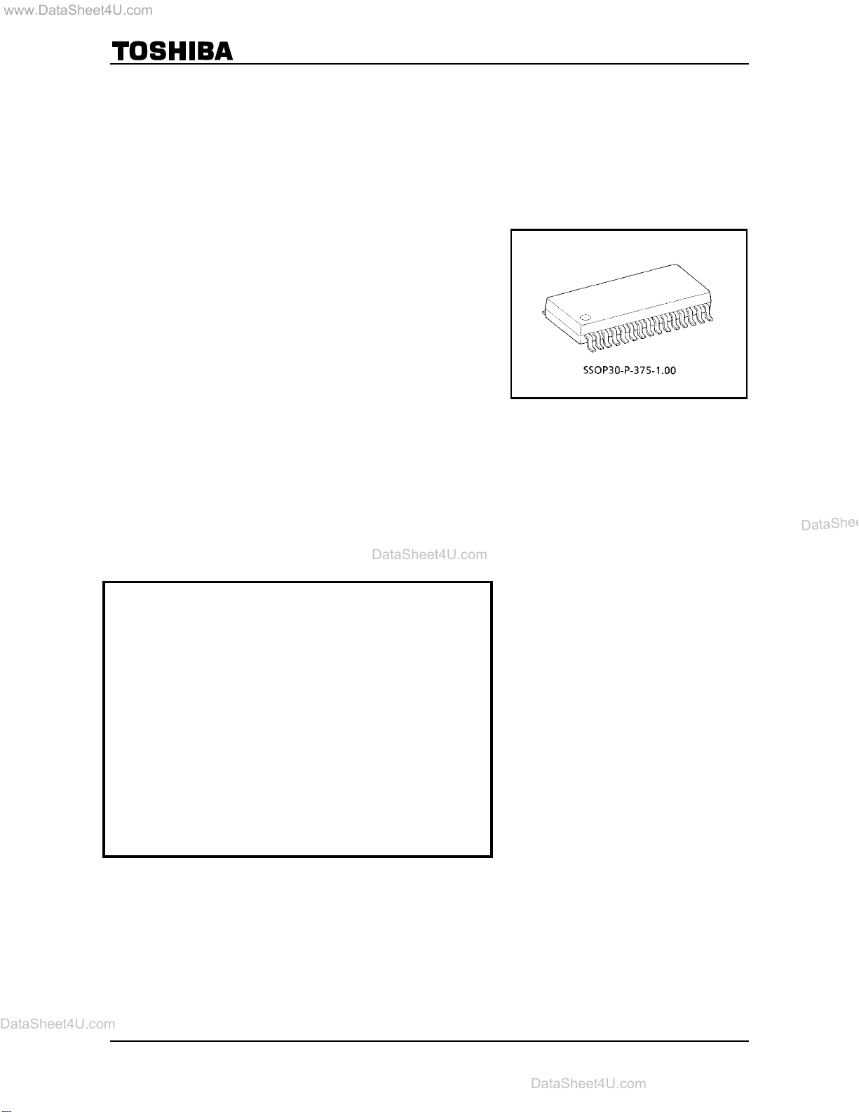
Package Dimensions
TB6556F/FG
Weight: 0.63 g (ty p.)
20
2005-01-19

www.DataSheet4U.com
DataSheet4U.com
DataSheet4U.com
DataSheet4U.com
DataSheet4U.com
TB6556F/FG
Notes on contents
1. Block Diagram s
Some of the functional blocks, circuits, or constants may be omitted or simplified in the block diagram for
explanatory purposes.
2. Equivalent Circuits
The equivale nt circuit diagr ams may b e simplified or some parts of them may be omi tted f or explanatory
purposes.
3. Timing Charts
Timing charts may be simplified for explanatory purposes.
4. Maximum Ratings
The absolute maximum ratings of a semiconductor device are a set of specif ied parameter values t hat must not
be exceeded during operation, even for an instant.
If any of these ratings are exceeded during operation, the electrical characteristics of the device may be
irreparably altered, in which case the reliability and lifetime of the device can no longer be guaranteed.
Moreover, any exceeding of the ratings during operation may cause breakdown, damage and/or degradation in
other equipment. Applications using the device should be designed so that no maximum rating will ever be
exceeded under any operating conditions.
Before using, creating and/or producing designs, refer to and comply with the precautions and conditions set
forth in this document.
5. Application Circuits
The application circuits shown in this document are provided for reference purposes only. Thorough evaluation
is required in the mass production design phase.
In furnishing these examples of application circuits, Toshiba does not grant the use of any industrial property
rights.
6. Test Circuits
Components in test circuits are used only to obtain and confirm device characteri stics. These compo nents and
circuits are not guaranteed to prevent malfunction or failure in application equipment.
Handling of the IC
Ensure that the product is installed correctly to pr event breakdown, damage and/o r degradation i n the product
or equipment.
Over-current protection and heat protection circuits
These protection functions are intended only as a temporary means of preventing out put short circuits or other
abnormal conditions and are not guaranteed to prevent damage to the IC.
If the guaranteed operating ranges of this product are exceeded, these protection features may not operate
and some output short circuits may result in the IC being damaged.
The over-current protection feature is intended to protect the IC from temporary short circuits only.
Short circu its per sisti ng over long periods may cau se excessive stress and damage the IC. Syste ms should
be configured so that any over-current condition will be eliminated as soon as possible.
Counter-electromotiv e force
When the motor reverses or stops, the effect of counter-electromoti ve for ce ma y cause the current to flow to the
power source.
If the power supply is not equipped with sink capability, the power and output pins may exceed the maximum
rating.
The counter-electromotive force of the motor will var y depending on the conditions of use and the features of
the motor. Therefore make sure there will be no damage to or operational problem in the IC, and no damage to
or operational errors in peripheral circuits caused by counter-electromotive force.
21
2005-01-19

www.DataSheet4U.com
DataSheet4U.com
DataSheet4U.com
DataSheet4U.com
TB6556F/FG
RESTRICTIONS ON PRODUCT USE
• The information contained herein is subject to change without notice.
• The information contained herein is presented only as a guide for the applications of our products. No
responsibility is assumed by TOSHIBA for any infringements of patents or other rights of the third parties which
may result from its use. No l icense is granted by implication or otherwi se under any patent or patent rights of
TOSHIBA or others.
• TOSHIBA is continually working to improve the quality and reliability of its products. Nevertheless, semiconductor
devices in general can malfunction or fail due to their inherent electrical sensitivity and vulnerability to physical
stress. It is the responsibility of the buyer, when utilizing TOSHIBA products, to comply with the standards of
safety in making a s afe design for the entire system, a nd to avoid situations in which a mal function or failure of
such TOSHIBA products could cause loss of human life, bodil y injury or damage to property.
In developing your designs, please ensure that TOSHIBA products are used within specified operating ranges as
set forth in the most recent TOSHIBA products specifications. Also, pleas e keep in mind the precautions and
conditions set forth in the “Handling Guide for Semiconductor Devices,” or “TOSHIBA Semiconductor Reliability
Handbook” etc..
• The TOSHIBA products listed in this document are intended for usage in general electronics applications
(computer, personal equi pment , offi ce equipm ent, m easur ing equipm ent, in dust r ial roboti cs, domest ic appliances,
etc.). These TOSHIBA products are neither intended nor warranted for usage in equipment that requires
extraordinarily high quality and/or reliability or a malfunction or failure of which may cause loss of human life or
bodily injury (“Unintended Usage”). Unintended Usage include atomic energy control instruments, airplane or
spaceship instruments, transportation instruments, traffic signal instruments, combustion control instruments,
medical instruments, all types of safety devices, etc.. Unintended Usage of TOSHIBA products listed in this
document shall be made at the customer’s own risk.
• The products described in this document are subject to the foreign exchange and foreign trade laws.
• TOSHIBA products should not be embedded to the dow nstream products which are prohibited to be pr oduced
and sold, under any law and regulations.
030619EBA
22
2005-01-19
 Loading...