

查询TB6551F供应商
TOSHIBA Bi-CM OS Integrated Circ uit Silicon Monolithic
TB6551F
3-Phase Full-Wave Sine-Wave PWM Brushless Motor Controller
Features
· Sine-wave PWM control
· Built-in triangular-wave generator
(carrier cycle = f
· Built-in lead angle control function (0° to 58° in 32 steps)
· Built-in dead time function (setting 2.6 µs or 3.8 µs)
· Supports bootstrap circuit
· Overcurrent protection signal input pin
· Built-in regulator (V
· Operating supply voltage range: V
/252 (Hz))
osc
= 5 V (typ.), 30 mA (max))
ref
CC
= 6 V to 10 V
Weight: 0.33 g (typ.)
TB6551F
1
2002-12-24
TB6551F
2002-12-24
V
Y
W
Td
10
Comparator
U
5
8
6
9
time
dead
Setting
Comparator
Comparator
Z
4
7
Switching
120°/180°
120/180
V
U
Phase
Phase
W
Phase
and
gate
Charger
OS
12
block
protection
HUHVHW
PWM
on/off
120°-
matrix
turn-on
LA
23
6-bit triangular
wave generator
Data
select
Comparator
2
Output
4 bits
Counter
5-bit AD
generator
System clock
Position detector
generator
waveform
Phase
matching
voltage
Internal
reference
Regulator
Rotating
direction
FG
Power-on
ST/SP
CW/CCW
ERR
GB
&
reset
Protection
reset
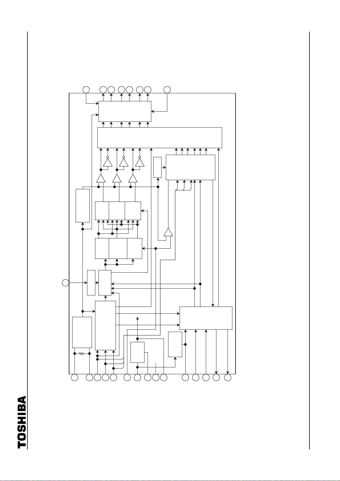
Block Diagram
1
V
CC
3
13
24
refout
V
S-GND
P-GND
14
15
21
20
19
22
in
out
X
HV
HU
X
HW
e
V
11
RES
3
18
17
16
dc
I
FG
REV
CW/CCW
Pin Description
Pin No. Symbol Description Remarks
TB6551F
21 HU
20 HV
19 HW
18 CW/CCW
11 RES Reset-signal-input pin
22 Ve
23 LA
12 OS
3 Idc
14 Xin Inputs clock signal
15 X
24 V
17 FG FG signal output pin Outputs 3PPR of positional signal
16 REV
9 U Outputs turn-on signal
8 V Outputs turn-on signal
7 W Outputs turn-on signal
6 X Outputs turn-on signal
5 Y Outputs turn-on signal
4 Z Outputs turn-on signal
1 VCC Power supply voltage pin VCC = 6 V~10 V
10 Td Inputs setting dead time L: 3.8 ms , H or Open: 2.6 ms
2 P-GND Ground for power supply Ground pin
13 S-GND Ground for signals Ground pin
refout
Positional signal
input pin U
Positional signal
input pin V
Positional signal
input pin W
Rotation direction
signal input pin
Inputs voltage instruction
signal
Lead angle setting signal
input pin
Inputs output logic select
signal
Inputs overcurrentprotection-signal
Outputs clock signal
out
Outputs reference voltage
signal
Reverse rotation detection
signal
When positional signal is HHH or LLL, gate block
protection operates.
With built-in pull-up resistor
L: Forward
H: Reverse
L: Reset (Output is non-active)
Operation/Halt operation
Also used for gate block protection
With built-in pull-down resistor
Sets 0° to 58° in 32 steps
L: Active low
H: Active high
Inputs DC link current.
Reference voltage: 0.5 V
With built-in filter (
With built-in feedback resistor
5 V (typ.), 30 mA (max)
Detects reverse rotation.
Select active high or active low using the output logic select pin.
~
-
1 ms)
3
2002-12-24
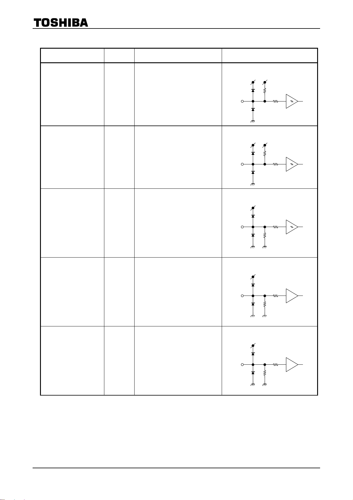
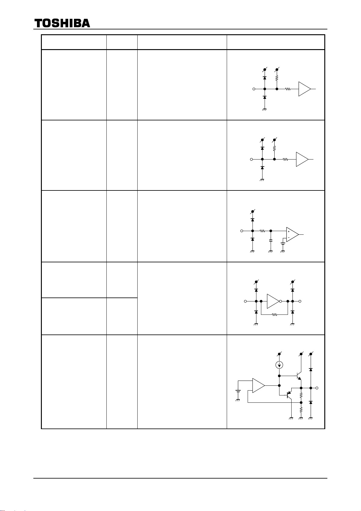
Input/Output Equivalent Circuits
Pin Description Symbol Input/Output Signal Input/Output Internal Circuit
TB6551F
Positional signal input pin U
Positional signal input pin V
Positional signal input pin W
Forward/reverse switching
input pin
L: Forward (CW)
H: Reverse (CCW)
Reset input
L: Stops operation (reset).
H: Operates.
Voltage instruction signal
input pin
Turn on the lower transistor
at 0.2 V or less.
(X, Y, Z pins: On duty of 8%)
Lead angle setting signal
input pin
0 V: 0°
5 V: 58°
(5-bit AD)
HU
HV
HW
CW/CCW
RES
V
e
LA
Digital
With Schmitt trigger
Hysteresis 300 mV (typ.)
L : 0.8 V (max)
H: V
Digital
With Schmitt trigger
Hysteresis 300 mV (typ.)
L : 0.8 V (max)
H: V
Digital
With Schmitt trigger
Hysteresis 300 mV (typ.)
L : 0.8 V (max)
H: V
Analog
Input range 0 V to 5.0 V
Input voltage of Vrefout or higher is
clipped to Vrefout.
Analog
Input range 0 V to 5.0 V
Input voltage of V
clipped to V
- 1 V (min)
refout
- 1 V (min)
refout
- 1 V (min)
refout
refout
refout
.
or higher is
V
V
V
refout
refout
refout
VCC
VCC
V
refout
refout
240 k9
2.4 kW
V
120 k9
2.4 kW
2.4 kW
120 k9
120 W
240 k9
120 W
240 k9
4
2002-12-24
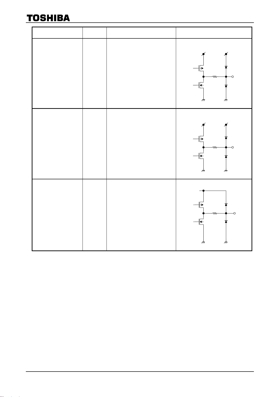
Pin Description Symbol Input/Output Signal Input/Output Internal Circuit
V
refout
Setting dead time input pin
L : 3.8 ms
H or Open: 2.6 ms
Td
Digital
L : 0.8 V (max)
refout
- 1 V (min)
H: V
V
Output logic select signal
input pin
L: Active low
H: Active high
Overcurrent protection
signal input pin
Clock signal input pin Xin
Clock signal output pin X
OS
I
dc
out
Digital
L : 0.8 V (max)
refout
- 1 V (min)
H: V
Analog
Gate block protected at 0.5 V or higher
(released at carrier cycle)
Operating range
2 MHz to 8 MHz (crystal oscillation)
X
refout
VCC
240 kW
5 pF
V
V
refout
in
360 kW
refout
1.2 kW
refout
2.4 kW
0.5 V
VCC
V
120 k9
V
120 k9
refout
TB6551F
Comparator
X
out
V
V
CC
CC
Reference voltage signal
output pin
Vrefout 5 ± 0.5 V (max 30 mA)
5
2002-12-24
Pin Description Symbol Input/Output Signal Input/Output Internal Circuit
refout
Digital
Reverse-rotation-detection
signal output pin
FG signal output pin FG
REV
Push-pull output: ± 1 mA (max)
Digital
Push-pull output: ± 1 mA (max)
120 W
refout
120 W
TB6551F
V
V
refout
V
V
refout
Turn-on signal output pin U
Turn-on signal output pin V
Turn-on signal output pin W
Turn-on signal output pin X
Turn-on signal output pin Y
Turn-on signal output pin Z
U
V
W
X
Y
Z
Analog
Push-pull output: ± 2 mA (max)
L : 0.78 V (max)
H: V
- 0.78 V (min)
refout
V
refout
120 W
6
2002-12-24
TB6551F
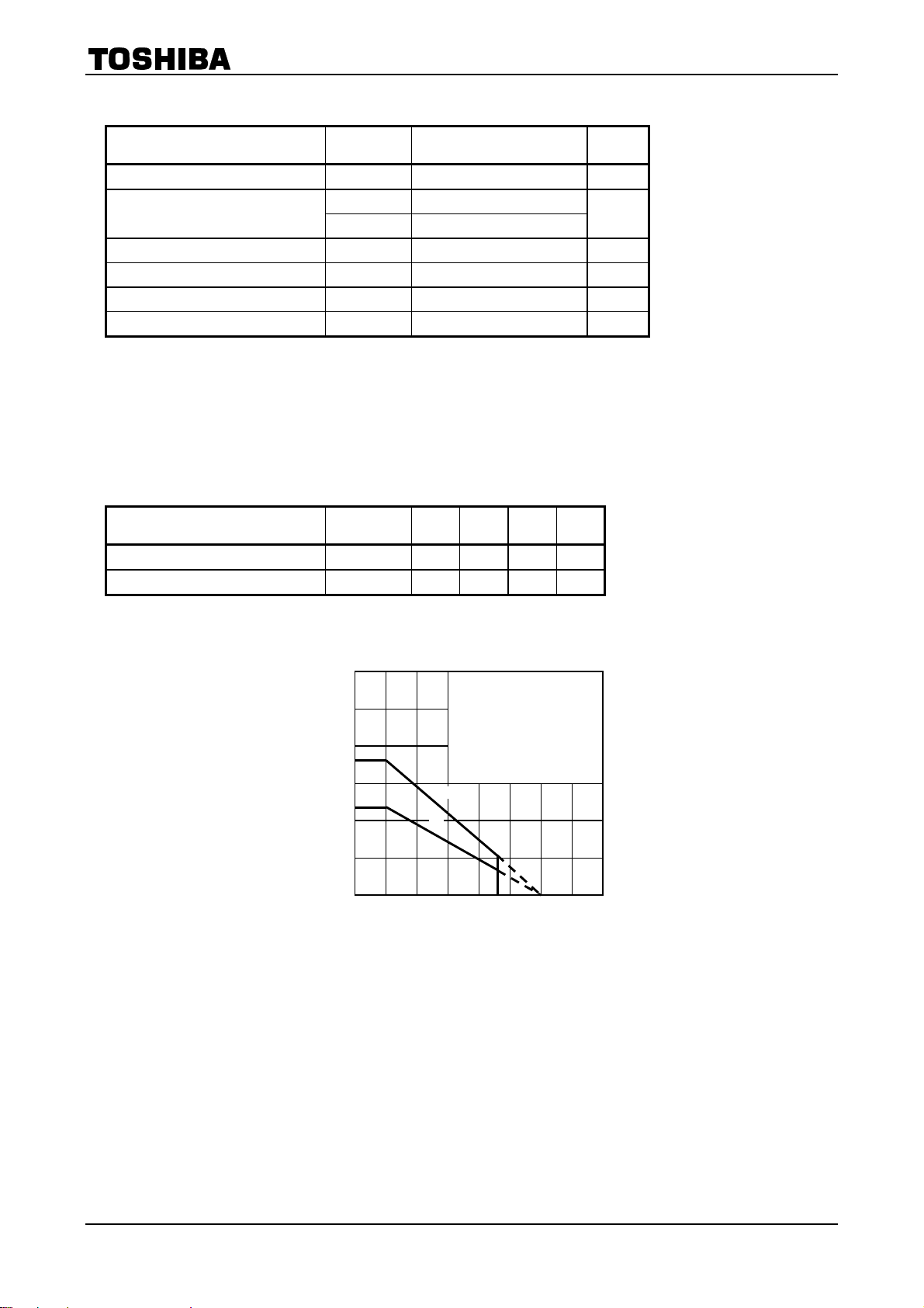
Maximum Ratings
Characteristics Symbol Rating Unit
Supply voltage VCC 12 V
Input voltage
Turn-on signal output current I
Power Dissipation PD 0.9 (Note 3) W
Operating temperature T
Storage temperature T
Note 1: V
Note 2: V
in (1)
in (2)
(Ta ==== 25°C)
pin: Ve, LA
pin: HU, HV, HW, CW/CCW, RES, OS, I
V
-0.3~VCC (Note 1)
in (1)
-0.3~5.5 (Note 2)
V
in (2)
2 mA
OUT
-30~115 (Note 4) °C
opr
-50~150 °C
stg
Td
dc,
V
Note 3: When mounted on PCB (universal 50 ´ 50 ´ 1.6 mm, Cu 30%)
Note 4: Operating temperature range is determined by the PD - Ta characteristic.
Recommended Operating Conditions
Characteristics Symbol Min Typ. Max Unit
(Ta ==== 25°C)
Supply voltage VCC 6 7 10 V
Crystal oscillation frequency Xin 2 4 8 MHz
1.5
(W)
1.0
D
0.5
Power dissipation P
(2)
– Ta
P
D
(1) When mounted on PCB
Universal
50 ´ 50 ´ 1.6 mm
Cu 30%
(2) IC only
R
th (j-a)
(1)
= 200°C/W
0
0
50 100 150 200
Ambient temperature Ta (°C)
7
2002-12-24

TB6551F
Electrical Characteristics
Characteristics Symbol
(Ta ==== 25°C, VCC ==== 15 V)
Test
Circuit
Supply current ICC ¾ V
I
V
in (1)
Iin
-1 Vin = 0 V HU, HV, HW -40 -20 ¾
Input current
Input voltage Vin
(2)
Iin
-2 Vin = 0 V CW/CCW, OS, Td -80 -40 ¾
(2)
-3
I
in (2)
High
¾
¾ HU, HV, HW , CW /CCW, RES , OS, Td
Low
Input hysteresis
voltage
Output voltage
Output leakage
current
Output off-time by
upper/lower transistor
(Note 1)
V
¾ HU, H V, HW, CW/ CCW , RES ¾ 0.3 ¾ V
H
V
OUT (H)-1
V
OUT (L)-1
V
V
V
V
V
T
T
I
I
I
REV (H)
¾
I
REV (L)
I
FG(H)
I
FG(L)
refout
I
V
L (H)
I
L (L)
OFF(H)
OFF(L)
¾
¾
= open ¾ 3 6 mA
refout
= 5 V Ve, LA ¾ 20 40
in
Vin = 5 V RES ¾ 40 80
= 2 mA U, V, W, X, Y, Z
OUT
= -2 mA U, V, W, X, Y, Z ¾ 0.4 0.78
OUT
= 1 mA REV
OUT
= -1 mA REV ¾ 0.5 1.0
OUT
= 1 mA FG
OUT
= -1 mA FG ¾ 0.5 1.0
OUT
I
= 30 mA V
OUT
= 0 V U, V, W, X, Y, Z ¾ 0 10
OUT
V
= 3.5 V U, V, W, X, Y, Z ¾ 0 10
OUT
Td = High or open, X
I
= ± 2 mA, OS = High/Low
OUT
Td = Low, X
I
= ± 2 mA, OS = High/Low
OUT
= 4.19 MHz,
in
Test Condition Min Typ. Max Unit
mA
V
4.5 5.0 5.5
refout
= 4.19 MHz,
in
refout
- 1
¾ ¾ 0.8
V
refout
- 0.78
V
refout
- 1.0
V
refout
- 1.0
2.2 2.6 ¾
3.0 3.8 ¾
¾ V
V
refout
- 0.4
V
refout
- 0.5
V
refout
- 0.5
refout
¾
¾
V
V
¾
mA
ms
Overcurrent detection Vdc ¾ Idc 0.46 0.5 0.54 V
T
Lead angle correction
VCC monitor
L
LA (0)
T
LA = 2.5 V, Hall IN = 100 Hz 27.5 32 34.5
LA (2.5)
L
T
LA (5)
V
Output start operation point 4.2 4.5 4.8
CC (H)
V
No output operation point 3.7 4.0 4.3
CC (L)
= 0 V or Open, Hall IN = 100 Hz ¾ 0 ¾
A
= 5 V, Hall IN = 100 Hz 53.5 59 62.5
A
°
V
VH Input hysteresis width ¾ 0.5 ¾
Note 5: T
OFF
OS = High
Turn-on signal (U, V, W)
Turn-on signal (X, Y, Z)
0.78 V 0.78 V
T
OFF
T
OFF
0.78 V
0.78 V
OS = Low
Turn-on signal (U, V, W)
V
refout
- 0.78 V
V
refout
- 0.78 V
Turn-on signal (X, Y, Z)
T
T
OFF
- 0.78 V V
V
refout
refout
- 0.78 V
8
OFF
2002-12-24

Functional Description
1. Basic operation
The motor is driven by the square-wave turn-on signal based on a positional signal. When the positional
signal reaches number of rotations f = 5 Hz or higher, the rotor position is assumed according to the
positional signal and a modulation wave is generated. The modulation wave and the triangular wave are
compared then the sine-wave PWM signal is generated and the motor is driven.
From start to 5 Hz: When driven by square wave (120° turn-on) f = f
5 Hz~: When driven by sine-wave PWM (180° turn-on) When f
2. Function to stabilize bootstrap voltage
(1) When voltage instruction is input at V
Turns on the lower transistor at regular (carrier) cycle. (On duty is approx. 8%)
(2) When voltage instruction is input at V
During sine-wave drive, outputs drive signal as it is.
During square-wave drive, forcibly turns on the lower transistor at regular (carrier) cycle.
(On duty is approx. 8%)
<
0.2 V:
e
> 0.2 V:
e
/(212 ´ 32 ´ 6)
osc
= 4 MHz, approx. 5 Hz
osc
TB6551F
Note: At startup, to charge the upper transistor gate power supply, turn the lower transistor on for a fixed
time with V
e
<
0.2 V.
3. Dead time function: upper/lower transistor output off-time
When driving the motor by sine-wave PWM, to prevent a short circuit caused by simultaneously turning
on upper and lower external power devices, digitally generates dead time in the IC.
When a square wave is generated in full duty cycle mode, the dead time function is turned on to prevent a
short circuit.
Td Pin Internal Counter T
High or Open 11/f
Low 16/f
T
values above are obtained when fosc = 4.19 MHz.
OFF
f
= reference clock (crystal oscillation)
osc
2.6 ms
osc
3.8 ms
osc
OFF
4. Correcting lead angle
The lead angle can be corrected in the turn-on signal range from 0 to 58° in relation to the induced
voltage.
Analog input from LA pin (0 V to 5 V divided by 32)
0 V = 0°
5 V = 58° (when more than 5 V is input, 58°)
5. Setting carrier frequency
Sets triangular wave cycle (carrier cycle) necessary for generating PWM signal.
(The triangular wave is used for forcibly turning on the lower transistor when driving the motor by
square wave.)
Carrier cycle = f
/252 (Hz) f
osc
= Reference clock (crystal oscillation)
osc
6. Switching the output of turn-on signal
Switches the output of turn-on signal between high and low.
Pin OS:
High = active high
Low = active low
9
2002-12-24

7. Outputting reverse rotation detection signal
Detects motor rotation direction every electrical degrees of 360°. (The output is high immediately after
reset)
REV terminal increases with a 180° turn-on mode at the time of low.
CW/CCW Pin Actual Motor Rotati ng Di rection REV Pin
TB6551F
Low (CW)
High (CCW)
8. Protecting input pin
1. Overcurrent protection (Pin Idc)
When the DC-link-current exceeds the internal reference voltage, performs gate block protection.
Overcurrent protection is released for each carrier frequency.
Reference voltage = 0.5 V (typ.)
2. Gate block protection (Pin RES)
When the input signal level is Low, turns off the output; when High, restarts the output.
Detects abnormality externally and inputs the signal to the pin RES.
RES Pin OS Pin
Low
(When RES = Low, bootstrap capacitor charging stops.)
3. Internal protection
· Positional signal abnormality protection
When the positional signal is HHH or LLL, turns off the output; otherwise, restarts the output.
· Low power supply voltage protection (V
When power supply is on/off, prevents damage caused by short-circuiting power device by
keeping the turn-on signal output at high impedance outside the operating voltage range.
Power supply
voltage
CW (forward) Low
CCW (reverse) High
CW (forward) High
CCW (reverse) Low
Output Turn-on Signal
(U, V, W, X, Y, Z)
Low High
High Low
monitor)
CC
4.5 V (typ.) 4.0 V (typ.)
V
CC
GND
Turn-on signal
Output at high impedance
10
V
M
Output at high impedance Output
2002-12-24

TB6551F
X
Operation Flow
Positional signal
(Hall IC)
Voltage
instruction
Oscillator
System clock
generator
Position
detector
Phase matching
(Note)
92%
Phase U
Counter
Phase V
Phase
W
Driven by square wave
Sine-wave pattern
(modulation signal)
Triangular wave
(carrier frequency)
U
V
Y
Comparator
W
Z
Output ON duty (U, V, W)
0.2 V (typ.)
Voltage instruction Ve
4.6 V
Note: Output ON time is decreased by the dead time.
(carrier frequency ´ 92% - T
´ 2)
d
100%
Driven by sine wave
Modulation ratio (modulation signal)
0.2 V (typ.)
0
Voltage instruction Ve
5 V (V
refout
)
11
2002-12-24
TB6551F
V
The modulation waveform is generated using Hall signals. Then, the modulation waveform is compared
with the triangular wave and a sine-wave PWM signal is generated.
The time (electrical degrees: 60°) from the rising (or falling) edges of the three Hall signals to the next
falling (or rising) edges are counted. The counted time is used as the data for the next 60° phase of the
modulation waveform.
There are 32 items of data for the 60° phase of the modulation waveform. The time width of one data
item is 1/32 of the time width of the 60° phase of the previous modulation waveform. The modulation
waveform moves forward by the width.
HU
HV
HW
S
U
S
V
Sw
(6) (1) (3)
(5) (2)
(6)’ (1)’ (2)’ (3)’
*HU, HV, HW: Hall signals
In the above diagram, the modulation waveform (1)’ data moves forward by the 1/32 time width of the
time (1) from HU: to HW: ¯. Similarly, data (2)’ moves forward by the 1/32 time width of the time (2) from
HW: ¯ to HV: .
If the next edge does not occur after the 32 data items end, the next 32 data items move forward by the
same time width until the next edge occurs.
*t
*t
32
31
30
6
5
4
3
2
1
S
* t = t(1) ´ 1/32
(1)’
32 data items
The modulation wave is brought into phase with every zero-cross point of the Hall signal.
The modulation wave is reset in synchronization with the rising and falling edges of the Hall signal at
every 60° electrical degrees. Thus, when the Hall device is not placed at the correct position or when
accelerating/decelerating, the modulation waveform is not continuous at every reset.
12
2002-12-24

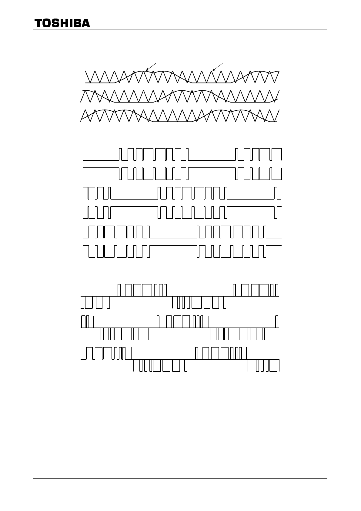
Timing Charts
X
X
H
Hall signal
(input)
u
H
v
H
w
TB6551F
FG signal
(output)
Turn-on signal
when driven
by square wave
(output)
Modulation
waveform when
driven by sine wave
(inside of IC)
FG
U
V
W
Y
Z
S
S
S
Hall signal
(input)
H
H
H
u
v
w
Forward
u
v
w
FG signal
(output)
Turn-on signal
when driven
by square wave
(output)
Modulation
waveform when
driven by sine wave
(inside of IC)
FG
U
V
W
Y
Z
S
S
S
u
v
w
Reverse
13
2002-12-24

TB6551F
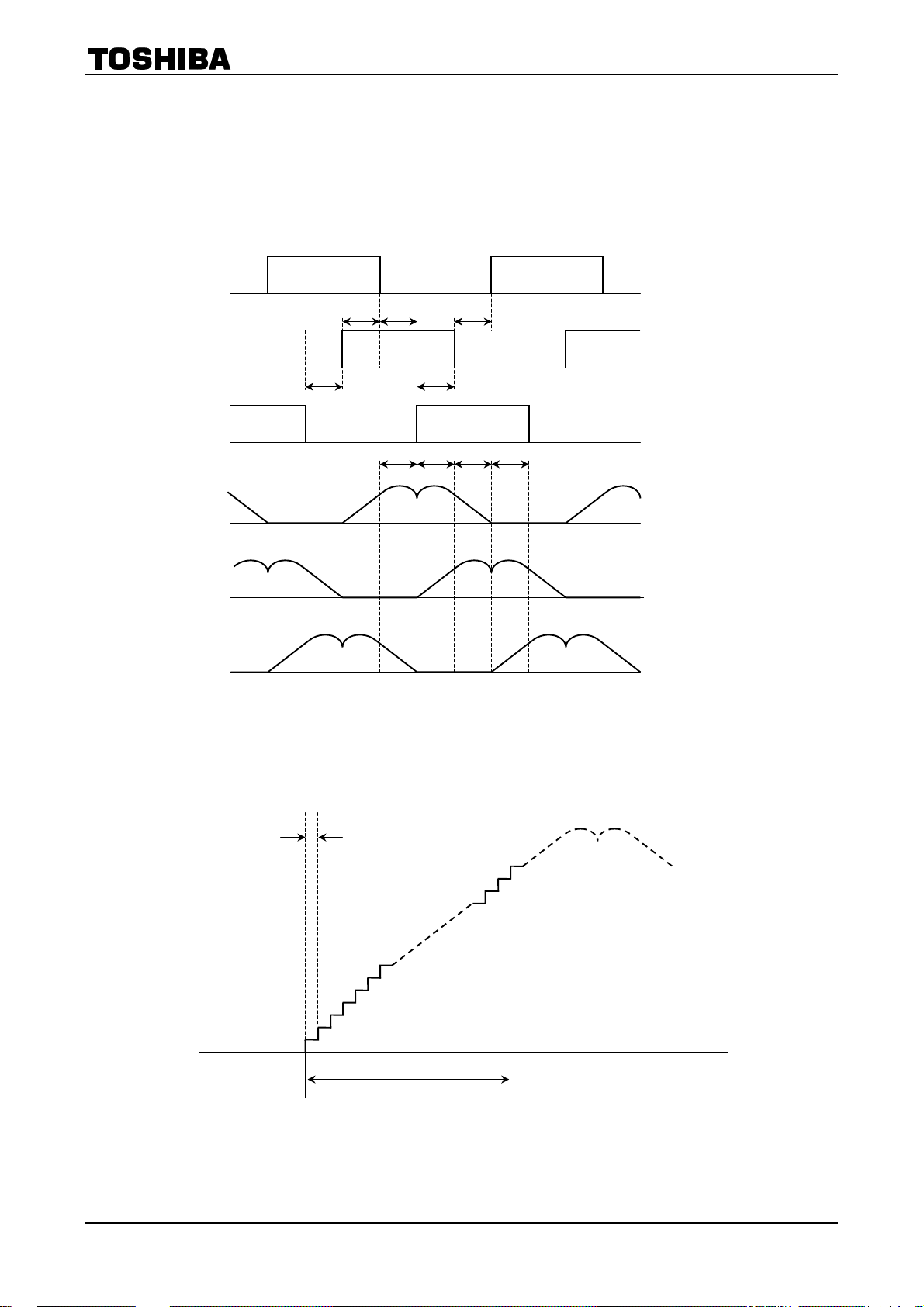
Operating Waveform When Driven by Square Wave
Hall signal
H
U
H
V
H
W
Output waveform
U
X
V
Y
W
(CW/CCW ==== Low, OS ==== High)
Z
Enlarged
waveform
W
Z
T
ONU
T
d
T
ONL
T
d
To stabilize the bootstrap voltage, the lower outputs (X, Y, and Z) are always turned on at the carrier cycle
even during off time. At that time, the upper outputs (U, V, and W) are assigned dead time and turned off
at the timing when the lower outputs are turned on. (T
Carrier cycle = f
T
= carrier cycle ´ 8% (s) (Uniformity)
ONL
/252 (Hz) Dead time: Td = 16/f
osc
varies with input Ve)
d
(s) (In more than Ve = 4.6 V)
osc
When the motor is driven by a square wave, acceleration/deceleration is determined by voltage V
motor accelerates/decelerates according to the On duty of T
(see the diagram of output On duty on
ONU
page 11).
Note: At startup, the motor is driven by a square wave when the Hall signals are 5 Hz or lower (f
the motor is rotating in the reverse direction as the TB6551F controls it (REV = High).
e
= 4 MHz) and
osc
. The
14
2002-12-24
TB6551F
Operating Wave form When Driven by Sine-Wave PWM
Generation inside of IC
Phase U
Phase V
Phase W
Output waveform
U
X
V
Y
Modulation signal
(CW/CCW ==== Low, OS ==== High)
Triangular wave (carrier frequency)
Inter-line voltage
When the motor is driven by a sine wave, the motor is accelerated/decelerated according to the On duty of
T
ONU
duty on page 11).
W
Z
V
UV
(U-V)
V
VW
(V-W)
V
WU
(W-U)
when the amplitude of the modulation symbol changes by voltage Ve (see the diagram of output On
Triangular wave frequency = carrier frequency = f
/252 (Hz)
osc
Note: At startup, the motor is driven by a sine wave when the Hall signals are 5 Hz or higher (f
motor is rotating in the same direction as the TB6551F controls it (REV = Low).
15
= 4 MHz) and the
osc
2002-12-24

r
f
g
pump)
(charge
Pre-drive
d
5 V
T
10
Comparator
U
9
V
Y
W
Z
4
7
5
8
6
Setting
dead time
Switching
Comparator
Comparator
120/180
&
120°/180°
Charger
OS
12
gate
block
on/off
protection
120°-
matrix
turn-on
(Note 1)
(Note 1)
HUHVHW
V
U
Phase
Phase
W
Phase
PWM
Triangular wave
generator 6-bit
data
Selecting
Comparator
Output
generator
waveform
4 bit
LA
23
Counter
5-bit AD
refout
V
generator
System clock
Position detector
Phase
Internal
ST/SP
CW/CCW
ERR
GB
Protection
BRK (CHG)
&
reset
matching
e
volta
reference
Rotating
FG
direction
reset
Power-on
Regulator
14
15
21
20
19
out
HV
HU
X
in
X
HW
22
1
e
V
V
CC
13
24
re
V
S-GND
P-GND
2
11
3
18
17
16
dc
I
RES
FG
REV
CW/CCW
(Note 2)
6 V to 10 V
MCU
Note 1: For preventing the IC from misoperation caused by noise for example connect to ground as required.
Note 2: Connect P-GND to signal ground on an application circuit.
Note 3: A short circ uit between the outputs, or between output and supply or ground may damage the device. Periferal parts may also be dameged by overvoltage and overcurrent. Design the output lines, V
Example of Application Circuit

Package Dimensions
TB6551F
Weight: 0.33 g (typ.)
17
2002-12-24

TB6551F
A
RESTRICTIONS ON PRODUCT USE
· TOSHIBA is continually working to improve the quality and reliability of its products. Nevertheless, semiconducto r
devices in general can malfunction or fail due to their inherent electrical sensitivity and vulnerability to physical
stress. It is the responsibility of the buyer, when utilizing TOSHIBA products, to comply with the standards of
safety in making a safe design for the entire system, and to avoid situations in which a malfunction or failure of
such TOSHIBA products could cause loss of human life, bodily injury or damage to property.
In developing your designs, please ensure that TOSHIBA products are used within specified operating ranges as
set forth in the most recent TOSHIBA products specifications. Also, please keep in mind the precautions and
conditions set forth in the “Handling Guide for Semiconductor Devices,” or “TOSHIBA Semiconductor Reliability
Handbook” etc..
· The TOSHIBA products listed in this document are intended for usage in general electronics applications
(computer, personal equipment, office equipment, measuring equipment, industrial robotics, domestic appliances,
etc.). These TOSHIBA products are neither intended nor warranted for usage in equipment that requires
extraordinarily high quality and/or reliability or a malfunction or failure of which may cause loss of human life or
bodily injury (“Unintended Usage”). Unintended Usage include atomic energy control instruments, airplane or
spaceship instruments, transportation instruments, traffic signal instruments, combustion control instruments,
medical instruments, all types of safety devices, etc.. Unintended Usage of TOSHIBA products listed in this
document shall be made at the customer’s own risk.
· The products described in this document are subject to the foreign exchange and foreign trade laws.
· The information contained herein is presented only as a guide for the applications of our products. No
responsibility is assumed by TOSHIBA CORPORATION for any infringements of intellectual property or other
rights of the third parties which may result from its use. No license is granted by implication or otherwise under
any intellectual property or other rights of TOSHIBA CORPORATION or others.
000707EB
· The information contained herein is subject to change without notice.
18
2002-12-24
 Loading...