

Toshiba Bi-CMOS Integrated Circuit Silicon Monolithic
y
(
Preliminar
TB6549F,TB6549P
Full-Bridge Driver IC for DC motor
TB6549F/P is a full-bridge driver IC for DC motor which uses
LDMOS for output transistors. High efficient drive is possible by
MOS process with low ON-resistor and PWM drive system. Four
modes such as CW, CCW, short brake, and stop can be chosen by
IN1 and IN2.
Features
• Power supply voltage: 30 V (max)
• Output current: 3.5 A (max)
• Low ON resistor: 0.5 Ω (typ.)
• Capable of PWM controlling
• Standby system
• CW/CCW/short brake/stop function modes.
• Built-in overcurrent protection
• Built-in thermal shutdown circuit
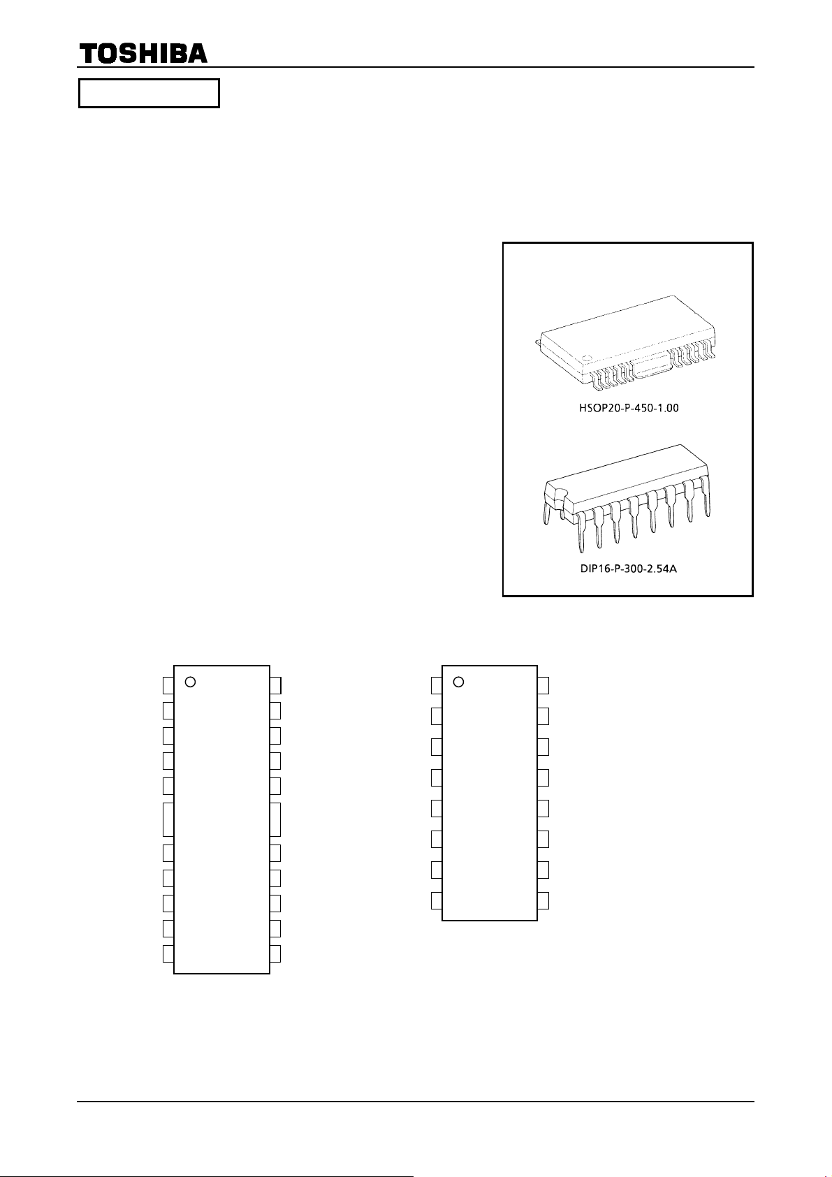
• Package: HSOP-20/DIP-16
Pin Assigument
HSOP20-P-450-1.00
DIP16-P-300-2.54A
TB6549F
TB6549P
Weight
HSOP20-P-450-1.00: 0.79 g (typ.)
DIP16-P-300-2.54A: 1.11 g (typ.)
TB6549F/P
N.C.
CcpA
CcpB
CcpC
N.C.
S-GND
Fin)
N.C.
IN1
IN2
N.C.
OUT1
Note: This product has a MOS structure and is sensitive to electrostatic discharge. When handling this product,
ensure that the environment is protected against electrostatic discharge by using an earth strap, a conductive
mat and an ionizer. Ensure also that the ambient temperature and relative humidity are maintained at
reasonable levels.
V
CC
N.C.
V
reg
SB
N.C.
S-GND
(Fin)
N.C.
PWM
N.C.
OUT2
P-GND
CcpA
CcpB
CcpC
S-GND
S-GND
IN1
IN2
OUT1
V
CC
V
reg
SB
S-GND
S-GND
PWM
OUT2
P-GND
1
2002-08-30
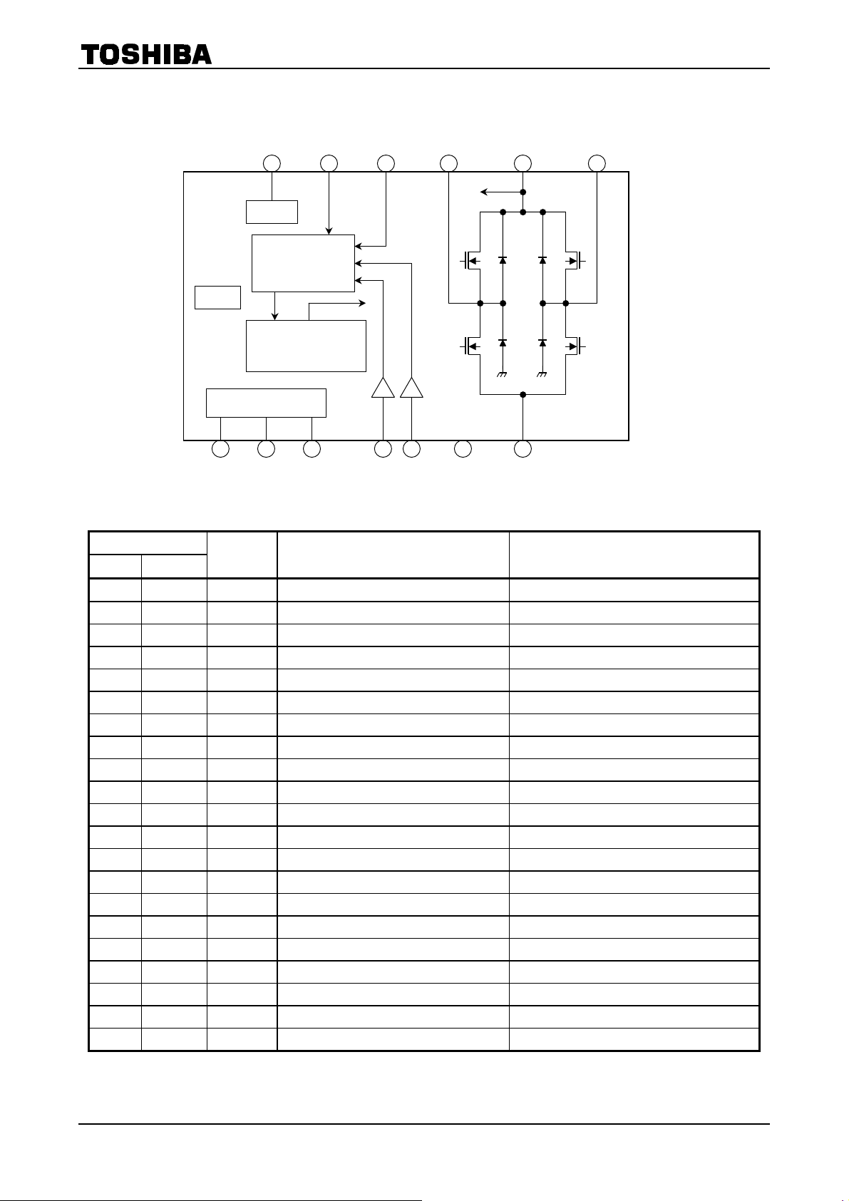
Block Diagram
V
reg
5 V
Control logic
OSC
Overcurrent
detecting circuit
T
SD
Charge pump circuit
PWM
CC
TB6549F/P
OUT1 OUT2 SB V
CcpA CcpB CcpC
IN1 IN2 P-GND
S-GND
Pin Functions
Pin No.
F P
1 (NC) No Connection
2 1 CcpA Capacitor connection pin for charge pump A Connect a capacitor for charge pump
3 2 CcpB Capacitor connection pin for charge pump B Connect a capacitor for charge pump
4 3 CcpC Capacitor connection pin for charge pump C Connect a capacitor for charge pump
5 (NC) No Connection
6 (NC) No Connection
7 6 IN1 Control signal input 1 Input 0/5-V signal
8 7 IN2 Control signal input 2 Input 0/5-V signal
9 (NC) No Connection
10 8 OUT1 Output pin 1 Connect to motor coil pin
11 9 P-GND Power GND
12 10 OUT2 Output pin 2 Connect to motor coil pin
13 (NC) No Connection
14 11 PWM PWM control signal input pin Input 0/5-V PWM signal
15 (NC) No Connection
16 (NC) No Connection
17 14 SB Standby pin H: Start, L: Standby
18 15 V
19 (NC) No Connection
20 16 VCC Power supply input pin V
FIN 4, 5, 12, 13 S-GND GND pin
Pin Name Functional Description Remarks
5 V output pin Connect a capacitor to S-GND
reg
= 10 to 27 V
CC (ope)
2
2002-08-30
TB6549F/P
Maximum Ratings
Characteristics Symbol Rating Unit
Supply voltage V
Output current
Power dissipation
Operating temperature T
Storage temperature T
(Ta ==== 25°C)
F
P
CC
IO (Peak)
(Ave) 2.0
I
O
PD
−20 to 85 °C
opr
stg
30 V
3.5
2.5
2.5
−55 to 150 °C
(Note 1)
(Note 2)
(Note 3)
A
W
Note 1: The maximum ratings must be observed strictly. Make sure that all the characteristics listed above never
exceed the maximum ratings.
Note 2: This value is obtained by 115 × 75 × 1.6 mm PCB mounting occupied 30% of copper area.
Note 3: This value is obtained by 50 × 50 × 1.6 mm PCB mounting occupied 50% of copper area.
Operating Range
(Ta ==== 25°C)
Characteristics Symbol Rating Unit
Supply voltage V
PWM frequency f
CC
CLK
10 to 27 V
100 kHz
3
2002-08-30
TB6549F/P
Electrical Characteristics
Characteristics Symbol
Supply current
Input voltage
Control circuit
PWM input circuit
Standby circuit
Output ON resistance R
Output leakage current
Diode forward voltage
Internal reference voltage V
Overcurrent detection offset time I
Charge pump rising time t
Thermal shutdown circuit operating
temperature
Hysteresis
voltage
Input current
Input voltage
Hysteresis
voltage
Input current
PWM frequency
Minimum clock
pulse width
Input voltage
Hysteresis
voltage
Input current
(VCC ==== 24 V, Ta ==== 25°C)
Test
Circuit
I
CC1
I
CC2
I
CC3
I
CC4
V
INH
V
INL
V
IN (HYS)
I
INH
I
INL
V
PWMH
V
PWML
V
PWM(HYS)
I
PWMH
I
PWML
f
PWM
tw(
PWM)
V
INSH
V
INSL
V
IN (HYS)
I
INSH
I
INSL
on (U + L)
I
L (U)
I
L (L)
V
F (U)
V
F (L)
reg
SD (OFF)
ONG
T
SD
CW/CCW mode 6 10
Short break mode 4 8
2 5.5
(Not tested) 0.2
V
V
2 5.5
(Not tested) 0.2
V
4
V
I
4 No load 4.5 5 5.5 V
(Not tested) 50 µs
7
(Not tested) 160 °C
Stop mode 4 8
1
(Standby mode) 1 2
2
0.8
= 5 V 50 75
IN
1
VIN = 0 V 5
3
(Not tested) 0.2
PWM
3
V
PWM
Duty = 50% 100 kHz
3
2 µs
2
0.8
= 5 V 50 75
IN
1
VIN = 0 V 5
Io = 0.2 A 1.0 1.75
= 1.5 A 1.0 1.75
I
o
= 30 V (Note 1) 150
CC
5
V
= 30 V 10
CC
= 1.5 A 1.3 1.7
o
6
I
= 1.5 A 1.3 1.7
o
= 0.22 µF, C2 = 0.01 µF
C
1
(Note 2)
Test Condition Min Typ. Max Unit
2 5.5
0.8
= 5 V 50 75
= 0 V 5
1 3 ms
mA
V
µA
V
µA
V
µA
Ω
µA
V
Note 1: Include the current in the circuit.
Note 2: C1 is a capacitor between CcpA and GND. C2 is a capacitor between CcpB and CcpC.
4
2002-08-30

Component Description
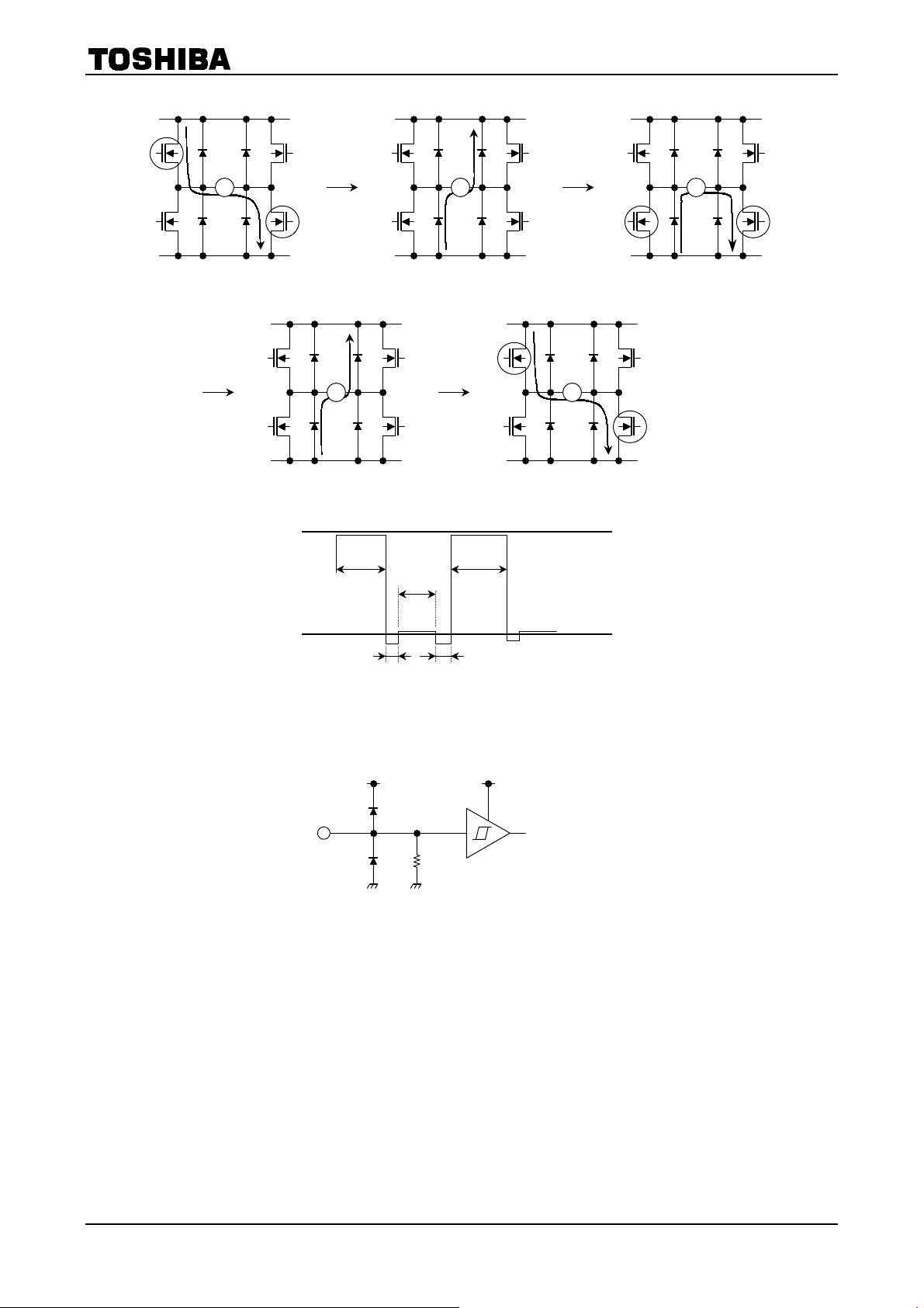
1. Control Input/PWM Input Circuit
VDD V
IN1
(IN2, PWM)
100 kΩ
• The input signals are shown below. Input at the CMOS and TTL levels can be provided. Note that the
input signals have a hysteresis of 0.2 V (typ.).
V
V
: 2 to V
INH
: GND to 0.8 V
INL
reg
V
• The PWM input frequency should be 100 kHz or less.
DD
Input/Output Function
Input Output
IN1 IN2 SB PWM OUT1 OUT2 Mode
H H H
L H H
H L H
L L H
H/L H/L L
• PWM control function
Motor speed can be controlled by inputting the 0/5-V PWM signal to the PWM pin.
When PWM control is provided, normal operation and short brake operation are repeated.
If the upper and lower power transistors in the output circuit were ON at the same time, a penetrating
current would be produced. To prevent this current from being produced, a dead time of 300 ns (design
target value) is provided in the IC when either of the transistors changes from ON to OFF, or vice versa.
Therefore, PWM control by synchronous rectification is enabled without an OFF time being inserted by
external input. Note that a dead time is also provided in the IC at the time of transition between CW
and CCW or between CW (CCW) and short brake mode, thereby eliminating the need for an OFF time.
H
L
H L H CW/CCW
L L L Short brake
H H L CCW/CW
L L L Short brake
H
L
H
L
L L Short brake
OFF
(high impedance)
OFF
(high impedance)
TB6549F/P
Stop
Standby
5
2002-08-30
TB6549F/P
VCC
VCC
VCC
OUT1 OUT1 OUT1
Output Voltage Waveform
M
GND
PWM ON
t1
VCC
M
PWM OFF → ON
t4 = 300 ns (typ.)
t1
(OUT1)
t2
M
PWM ON → OFF
t2 = 300 ns (typ.)
OUT1 OUT1
GND
t5
t3
t4
GND
PWM ON
t5
M
V
CC
GND
M
GND
PWM OFF
t3
VCC
GND
Note: Please set the pin PWM to High when PWM control function is not used.
2. Standby Circuit
VDD V
SB
100 kΩ
• All circuits are turned off except the standby circuit and the charge pump circuit under the standby
condition.
• Input voltage range is shown below. Input at CMOS and TTL level is possible. Input signal has 0.2-V
(typ.) hysteresis.
V
V
: 2 to V
INSH
: GND to 0.8 V
INSL
reg
V
• Please avoid controlling the output by inputting PWM signal to the standby pin. The output signal
becomes unstable and it may cause the destruction of the IC.
• The charge pump circuit is turned On/Off by the switch of the input signal from the standby pin. If the
switching cycle is shorter than 50 ms, the charge pump circuit will not operate with precise timing.
Therefore, switching cycle of the standby pin should be longer than 50 ms.
• When the Standby condition is changed to the Operation Mode, set IN1 and IN2 to Low level (Stop
Mode) at first. Then switch IN1 and IN2 to High level when the charge pump circuit reaches the stable
condition, VcpA is about V
CC
+ 5 V.
DD
6
2002-08-30

3. Internal Constant-Voltage (5 V) Circuit
VCC
VCC
V
reg
• This IC includes a 5-V power supply for control circuit.
• A capacitor for prevention of oscillation should be connected to S-GND associated with the pin V
No other loads should be connected to pin V
• This IC has a power monitoring function and turns the output OFF when V
reg
.
goes down to 3.0 V
reg
(design target value) or less. With a hysteresis of 0.3 V (design target value), the output are turned ON
when V
reaches 3.3 V (design target value) again .
reg
4. Charge Pump Circuit
VCC
CcpA
TB6549F/P
.
reg
CcpB
CcpC
• This IC has a charge pump circuit for driving the gate for the upper power transistor in the output
circuit. A voltage of V
It takes about 2 ms to boost V
+ 5 V (typ.) is generated by connecting an external capacitor to this IC.
CC
CPA
up V
+ 5 V (typ.) after the switch of the input signal from the
CC
standby pin. (while CcpA = 0.22 µF, and CcpB and CcpC are connected through 0.01 µF).
• The proper capacitance of the external capacitor varies depending on the V
CC value
. Thus, determine
the constant by referring to the following data. The value of the capacitor between CcpB and CcpC
should be such that, while the motor is being driven, the voltage on the CcpA pin will be kept constant,
typically at V
+ 5 V. (If a reduced VCC level causes the voltage on CcpA to start to fall, please adjust
CC
this capacitance value accordingly.)
<External capacitor>
VCC Between CcpB and CcpC Between CcpA and GND
10 V~15 V 0.01 µF~0.047 µF 0.22 µF
15 V~27 V 0.01 µF 0.22 µF
• Reference oscillation is performed by using the internal capacitor.
7
2002-08-30

5. Output Circuit
t
VCC
OUT1
(OUT2)
P-GND
• This IC uses Nch MOS transistors as the upper and lower transistors in the output circuit.
• As output R
• The switching characteristics of the output transistors are shown below.
PWM Input
is 1 Ω (sum for the upper and lower parts/typ.), this IC is a device of the low R
on
t
pLH
t
pHL
TB6549F/P
type.
on
Output Voltage
(OUT1/OUT2)
<Typical Value>
Item Typical Value Unit
t
350
pLH
t
800
pHL
tr 60
tf 100
<Actural Measured Waveform>
t
pLH
(350 ns)
PWM inpu
10%
ns
90%
50%
t
r
90%
50%
10%
t
f
t
pLH
(800 ns)
Output voltage
*: OUT 1, OUT 2; open
t
r
(60 ns)
(100 ns) t
f
8
2002-08-30

6. VCC Power Supply Section
• The V
circuit.
• The operating voltage range is shown below.
V
• This IC has a power monitoring function for preventing an output malfunction on power-up. However,
Toshiba recommends that IN1, IN2, and SB be set to the Low level at power-on.
power supply delivers a voltage to the output circuit, charge pump circuit, and internal 5-V
CC
CC (opr.)
= 10 to 27 V
7. GND Sections
• This IC includes two separate GND sections: S-GND for controlling and P-GND for outputting. Be sure
to short- circuit these two GNDs as close to TB6549 as possible.
8. Power Monitoring Circuit
• This circuit turns the output OFF when V
V
= 4.6 V (typ.)
CC
• With a hysteresis of 0.3 V (design target value), the output turns back ON when V
(design target value) after this circuit starts operating.
9. Thermal Shutdown (TSD) Circuit
This IC includes a thermal shutdown circuit which turns the output OFF when the junction temperature
(Tj) exceeds 160°C (typ.). The output turns back ON automatically. The thermal hysteresis is 20°C.
T
∆T
= 160°C (design target value)
SD
= 20°C (design target value)
SD
10. Overcurrent Detection (ISD) Circuit
This IC includes a circuit which detects a current flowing through the output power transistors. The
current limit is set to 5 A (typ.). The circuit detects a current flowing through each of the four output power
transistors. If the current in any one output power transistor exceeds the set limit, this circuit turns all the
outputs OFF.
This circuit includes a timer which causes the outputs to be OFF for 50 µs (typ.) after detection of an
overcurrent and then turn back ON automatically. If the overcurrent continues to flow, this ON-OFF
operation is repeated. Note that to prevent a malfunction due to a glitch, an insensitive period of 10 µs
(typ.) is provided.
I
LIM
TB6549F/P
becomes 3.0 V (design target value) or less. At this time,
reg
exceeds 3.3 V
reg
Output Current
0
50 µs
(typ.)
10 µs
(typ.)
Insensitive period
50 µs
(typ.)
10 µs
(typ.)
The set limit is 5 A (typ.) as a design target value. The distributions shown below exist because of the
variations in thermal characteristics of different ICs. These distributions should be fully considered in the
motor torque design.
Also, output peak current should be less than 3 A because of the variations below,
Detected current: Approximately from 3.5 to 6.5 A
9
2002-08-30

Test Circuit
V
V
V
V
V
V
V
V
TB6549F/P
1. Icc1, Icc2, Icc3, Icc4, I
INH
, I
INL
, I
INSH
, I
INSL
ICC
V
V
CC
OUT1
OUT2
5V/0
5V/0
5V/0
5
PWM
A IN1
I
IN
A IN2
I
IN
A SB
I
INS
TB6549F/P
P-GND S-GND
reg
CcpC CcpB CcpA
• Icc1: IN1 = 0 V, IN2 = 0 V, SB = 5 V
• Icc2: IN1 = 5 V, IN2 = 5 V, SB = 5 V or IN1 = 0 V, IN2 = 5 V, SB = 5 V
• Icc3: IN1 = 5 V, IN2 = 5 V, SB = 5 V
• Icc4: IN1 = 5 V/0 V, IN2 = 5 V/0 V, SB = 0 V
• I
• I
• I
• I
: IN1 = 5 V, and IN2 = 5 V
INH
: IN2 = 0 V, and IN2 = 0 V
INL
: SB = 5 V
INSH
: SB = 0 V
INSL
2. V
INH
, V
INL
, V
INSH
, V
INSL
A
24V
24V
CcpC CcpB CcpA
reg
5
PWM
IN1 2V/0.8
V
V
CC
OUT1
TB6549F/P
10
OUT2
V
V
2002-08-30
IN2 0.8V/2
SB 2V/0.8
P-GND S-GND
• V
• V
, V
INH
: IN1 = 0.8 V, IN2 = SB = 2 V, Verify that OUT1 = L, OUT2 = H. IN1 = SB = 2 V, IN2 = 0.8 V, Verify
INL
: IN1 = IN2 = SB = 2 V, Verify that OUT1 = OUT2 = L.
INSH
that OUT1 = OUT2 = L.
• V
: IN1 = IN2 = 2 V, SB = 0.8 V, Verify that output function is high impedance.
INSL

TB6549F/P
V
V
V
V
V
V
V
3. V
PWMH
, V
5V/0
2V/0.8V
100kHz
5V
I
PWM
A
• V
PWMH
• V
PWMH
• tw
(PWM)
4. Ron (H + L), Vreg
PWML
, I
PWM
IN1
PWMH
, I
PWML
, f
PWM
, tw
reg
(PWM)
CcpCCcpB CcpA
V
CC
24V
V
OUT1
TB6549F/P
IN2 0
SB 5
P-GND S-GND
, V
, V
, f
PWML
PWML
: PWM = 2 V/0.8 V, 100 kHz, dury: 50 % (rectangle wave), Verify out1
PWM
: PWM = 5 V or PWM = 0 V.
: PWM = 2 V/0.8 V, 100 kHz、dury: 20 % (2 µs) (2 µs/rectangle wave), Verify out1
OUT2
V
V
→
24V
IO
V
5V/0
V
CcpC CcpB CcpA
reg
5
PWM
IN1
V
V
CC
OUT1
TB6549F/P
IN2 0V/5
SB 5
P-GND S-GND
• Ron (H + L): Measure Vds (Sum of upper and lower side) at IO = 0.2 A, and change it to resistor. Same as
at I
= 1.5 A.
O
• Vreg: Vreg pin Voltage.
OUT2
IO
↓
V
11
2002-08-30

TB6549F/P
V
V
V0V
V
V
V0V
5. I
6. V
L (U)
5
F (U)
, I
, V
L (L)
F (L)
30V
A
I
L(L)
V
V
CC
OUT1
PWM
IN1
reg
CcpC CcpB CcpA
TB6549F/P
IN2 0
SB 5
P-GND S-GND
OUT2
A
I
L(H)
V
→
F(H)
24V
IO
V
V
V
CcpC CcpB CcpA
reg
5
PWM
IN1
CC
V
OUT1
TB6549F/P
IN2 0
SB 5
P-GND S-GND
• V
F (U)
, V
F (L)
: I
O
= 1.5 A.
OUT2
IO
↓
V
V
F(L)
12
2002-08-30

TB6549F/P
V
7. t
ONG
24V
V
V
CcpCCcpB CcpA
reg
5
PWM
IN1 0V
CC
V
OUT1
TB6549F/P
IN2 0V
SB 0V → 5V
P-GND S-GND
• t
: SB = 0 V → 5 V. Measure the time to boost CcpA voltage up about 29 V (24 V + 5 V)
ONG
OUT2
13
2002-08-30

TB6549F/P
3.0
(1)
P
2.4
(W)
D
1.8
(2)
1.2
– Ta (TB6549P)
D
(1) When mounted on PCB
(50 × 50 × 1.6mm glass-epoxy
PCB mounting occupied 50% of
copper area.)
(2) IC only
Power dissipation P
0.6
0
0
Ambient temperature Ta (°C)
External Attachments
Symbol Use
C1 Charge pump 0.22 µF
C2 Charge pump
C3 Prevention of V
C4 Absorption of power noise 0.001 µF to 1 µF
C5 Absorption of power noise 50 µF to 100 µF
oscillation 0.1 µF to 1.0 µF
reg
– Ta (TB6549F)
P
D
6
MAX (W)
D
240 40 80 120 160 200
Recommended
Value
4
(Note)
2
No heat sink
Maximum power dissipation P
0
0 50 100 150 200
Ambient temperature Ta (°C)
Remarks
Thermal resistance
R
= 13°C/W
th (j-c)
R
= 130°C/W
th (j-a)
Note: 50 × 50 × 1 mm
Fe heat sink
Infinite heat sink
3
0.01 µF VCC = 24 V (Note)
0.033 µF V
= 12 V (Note)
CC
Note: The recommended values for charge pumps depend on the VCC value. Please refer to the Component
Description 4, Charge Pump Circuit.
14
2002-08-30

Typical Application Diagram
5 V
V
DD
PWM
PORT1
PORT2
PORT3
GND
Microcontroller
20/16
V
OUT1
CC
C
Note 1
4
10/8
14/11
7/6
C
PWM
IN1
1
2/1
CcpA CcpB CcpC
3/2
Note 4
C
2
C
3
4/3
18/15
V
reg
TB6549F/P
8/7
IN2
17/14
SB
TB6549F: Pins 1, 5, 6, 9, 13, 15, 16, and 19 are not connected.
S-GND
FIN/4,5,12,13
P-GND
11/9
Note 5
Note 3
OUT2
12/10
TB6549F/TB6549P
TB6549F/P
C5
24V
M
Note 2
Note 1: Connect VCC and P-GND through the power supply capacitor. This capacitor should be as close as possible
to the IC.
Note 2: When connecting the motor pins through the capacitor for reducing noise, connect a resistor to the capacitor
for limiting the charge current. The switching loss increases for PWM control. Therefore, whenever
practicable, avoid connecting the capacitor if PWM control is required.
Note 3: Short-circuit S-GND and P-GND as close to TB6549 as possible.
Note 4: Connect the capacitor C
to S-GND.
3
Note 5: Connect the capacitors C1 and C2 as close to TB6549 as possible, and the capacitor C1 as close to S-GND.
Note 6: Pins 4, 5, 12, and 13 of the P type are connected to the chip’s bed. Therefore, expanding their round area
produces a better heat radiation effect.
Usage Precautions
• This IC includes an overcurrent detection circuit. However, if a short circuit takes place between output pins or
if an output pin is connected to the voltage source or ground, a heavy current temporarily flows through the IC.
It might destroy the IC. This possibility should be fully considered in the design of the output line, V
and GND line. If the IC is destroyed, a heavy current might continuously flow through it as a secondary effect.
Therefore, Toshiba recommends that a fuse be connected to the power supply line.
• Install this IC properly. If not, (e.g., installing it in the wrong position), the IC might be destroyed.
CC
line,
15
2002-08-30

Package Dimensions
TB6549F/P
Weight: 0.79 g (typ.)
16
2002-08-30

Package Dimensions
TB6549F/P
Weight: 1.11 g (typ.)
17
2002-08-30

TB6549F/P
A
RESTRICTIONS ON PRODUCT USE
• TOSHIBA is continually working to improve the quality and reliability of its products. Nevertheless, semiconductor
devices in general can malfunction or fail due to their inherent electrical sensitivity and vulnerability to physical
stress. It is the responsibility of the buyer, when utilizing TOSHIBA products, to comply with the standards of
safety in making a safe design for the entire system, and to avoid situations in which a malfunction or failure of
such TOSHIBA products could cause loss of human life, bodily injury or damage to property.
In developing your designs, please ensure that TOSHIBA products are used within specified operating ranges as
set forth in the most recent TOSHIBA products specifications. Also, please keep in mind the precautions and
conditions set forth in the “Handling Guide for Semiconductor Devices,” or “TOSHIBA Semiconductor Reliability
Handbook” etc..
• The TOSHIBA products listed in this document are intended for usage in general electronics applications
(computer, personal equipment, office equipment, measuring equipment, industrial robotics, domestic appliances,
etc.). These TOSHIBA products are neither intended nor warranted for usage in equipment that requires
extraordinarily high quality and/or reliability or a malfunction or failure of which may cause loss of human life or
bodily injury (“Unintended Usage”). Unintended Usage include atomic energy control instruments, airplane or
spaceship instruments, transportation instruments, traffic signal instruments, combustion control instruments,
medical instruments, all types of safety devices, etc.. Unintended Usage of TOSHIBA products listed in this
document shall be made at the customer’s own risk.
• The products described in this document are subject to the foreign exchange and foreign trade laws.
• The information contained herein is presented only as a guide for the applications of our products. No
responsibility is assumed by TOSHIBA CORPORATION for any infringements of intellectual property or other
rights of the third parties which may result from its use. No license is granted by implication or otherwise under
any intellectual property or other rights of TOSHIBA CORPORATION or others.
000707EB
• The information contained herein is subject to change without notice.
18
2002-08-30
 Loading...