

TB6552FN/FL
Toshiba Bi-CD Integrated Circuit Silicon Monolithic
TB6552FN,TB6552FL
Dual-Bridge Driver IC for DC motor
TB6552FN/FL is a dual-bridge driver IC for DC motor with
output transistor in LD MOS structure with low ON-resistor. Two
input signals, IN1 and IN2, can chose one of four modes such as
CW, CCW, short brake, and stop mode. Efficient driven at high
temperature is possible by PWM drive system.
TB6552FN
Features
· Power supply voltage for motor: VM ≤ 15 V (max)
· Power supply voltage for control: V
· Output current: 1 A (max)
· Low ON resistor: 1.5 Ω (typ.)
(Upper side + Lower side combined @ VM = 5 V)
· Direct PWM control
· Standby system (Power save)
· CW/CCW/short brake/stop function modes.
· Built-in thermal shutdown circuit
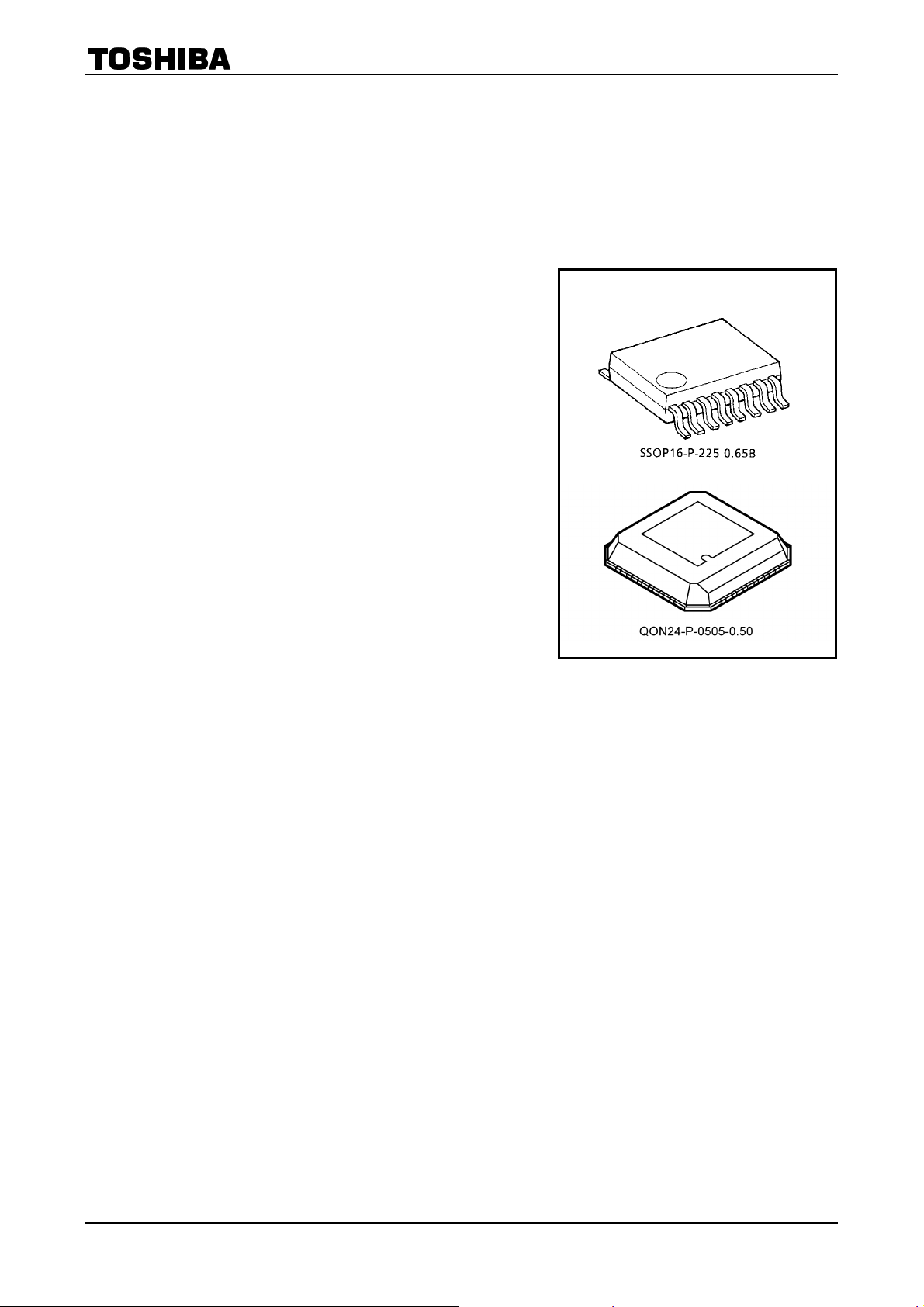
· Package: SSOP16 for TB6552FN /QON24 for TB6552FL
* This product has a MOS structure and is sensitive to electrostatic discharge. When handling this product,
ensure that the environment is protected against electrostatic discharge by using an earth strap, a conductive
mat and an ionizer. Ensure also that the ambient temperature and relative humidity are maintained at
reasonable levels.
= 2.7 V to 6.0 V
CC
TB6552FL
Weight
SSOP16-P-225-0.65B : 0.07 g (typ.)
QON24-P-0505-0.50 : 0.05 g (typ.)
1
2002-09-11
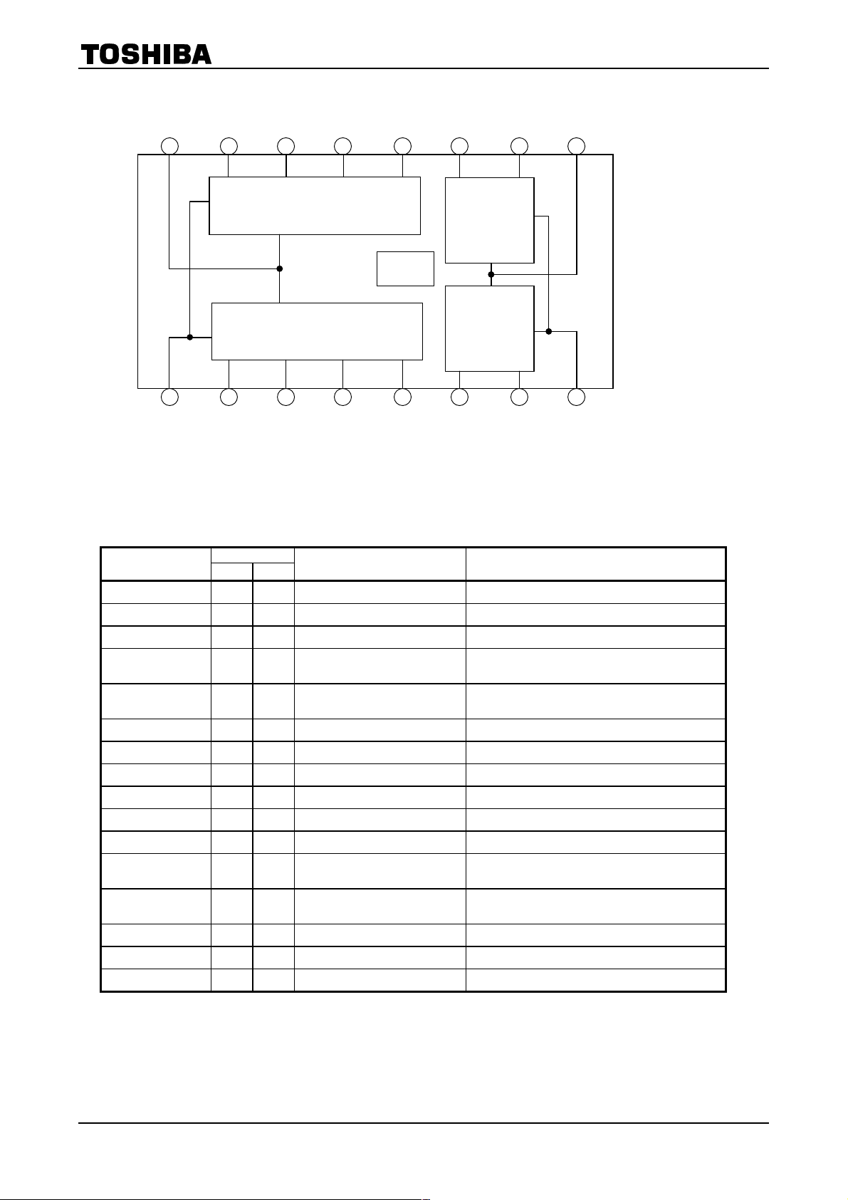
Block Diagram
TB6552FN/FL
VCC BSTBY
GND ASTBY
Pin Functions
BIN1 BIN2 BPWM
Control logic (Ch. B)
Control logic (Ch. A)
AIN1 AIN2 APWM
TSD
BO1
AO1
BO2
Bridge Driver
(Ch. B)
Bridge Driver
(Ch. A)
AO2
VM
PGND
Pin.Name
GND 1 21 Small-signal GND pin GND for small-signal power supply (VCC)
AIN1 2 18 Control signal input 1 (Ch. A)
AIN2 3 17 Control signal input 2 (Ch. A)
APWM 4 16
ASTBY 5 15
AO1 7 13 Output pin 1 (Ch. A) Ch. A connect to motor coil pin
AO2 8 11 Output pin 2 (Ch. A) Ch. A connect to motor coil pin
PGND 9 10 GND pin for motor GND for motor power supply (VM)
VM 6 14 Motor power supply pin VM (ope) = 2.5 V to 13.5 V
BO2 10 8 Output pin 2 (Ch. B) Ch. B connect to motor coil pin
BO1 11 5 Output pin 1 (Ch. B) Ch. B connect to motor coil pin
BSTBY 12 4
BPWM 13 3
BIN2 14 2 Control signal input 2 (Ch. B)
BIN1 15 1 Control signal input 1 (Ch. B)
VCC 16 22 Small-signal power supply pin VCC
Pin No
FN FL
Functional Description Remarks
PWM control signal input pin
(Ch. A)
Standby control input pin
(Ch. A)
Standby control input pin
(Ch. B)
PWM control signal input pin
(Ch. B)
Input PWM signal
Ch. A circuit is in standby (power save) state
while this signal is Low.
Ch. B circuit is in standby (power save) state
while this signal is Low.
Input PWM signal
= 2.7 V to 5.5 V
(ope)
Note: Pins 6, 7, 9, 12, 19, 20, 23 and 24 on the FL are NC (not connected) pins.
2
2002-09-11
TB6552FN/FL
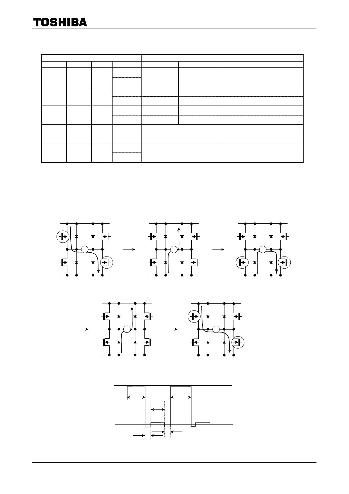
Input/Output Function
(common for channel A and B)
Input Output
IN1 IN2 STBY PWM O1 O2 Mode
H H H
L H H
H L H
L L H
H/L H/L L
H
L
H L H CW/CCW
L L L Short brake
H H L CCW/CW
L L L Short brake
H
L
H
L
L L Short brake
OFF
(high impedance)
OFF
(high impedance)
Operating Description
· PWM control function
Speed can be controlled by inputting the high-level or low-level PWM signal to the pin PWM.
When PWM control is provided, normal operation and short brake operation are repeated.
To prevent penetrating current, dead time t2 and t4 is provided in the IC.
VM
VM
Stop
Standby
VM
O1 O2
Output Voltage Waveform
M
PWM ON
t1
(O1)
O1
GND
O1 O2
M
PWM OFF ® ON
t4 = 300 ns (typ.)
t1
M
PWM ON ® OFF
t2 = 300 ns (typ.)
VM
GND
t5
t3
O2
GND
O1 O2
M
PWM ON
t5
O1 O2
VM
GND
V
CC
M
GND
PWM OFF
t3
t2
t4
Note: Please set the pin PWM to High when PWM control functionn is not used.
3
GND
2002-09-11
TB6552FN/FL
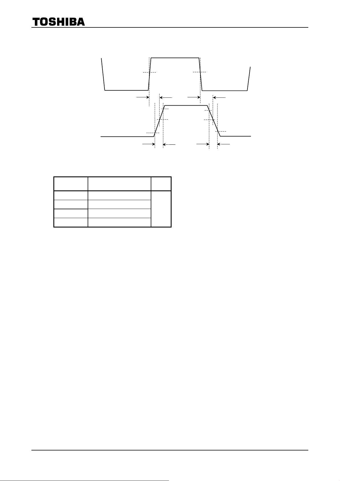
· Switching characteristics of output transistors
The switching characteristics between PWM input and the output transistors are shown below.
PWM Input
(APWM, BPWM)
t
pLH
t
pHL
Output Voltage
(A01, A02, B01, B02)
10%
90%
50%
t
r
90%
50%
10%
t
f
<Typical Value>
Item Typical Value Unit
t
1000
pLH
t
1000
pHL
tr 100
tf 100
ns
· Input pin
Input pins (AIN1, AIN2, APWM, ASTBY, BIN1, BIN2, BPWM and BSTBY) have internal pull-down
resistors that are connected to ground.
4
2002-09-11

TB6552FN/FL
Maximum Ratings
Characteristics Symbol Rating Unit Remarks
Supply voltage
Input voltage VIN -0.2 to 6 V IN1, 2, STBY and PWM pins
Output current I
Power dissipation PD
Operating temperature T
Storage temperature T
(Ta ==== 25°C)
VM
V
6
CC
1 A
OUT
-20 to 85 °C
opr
stg
15
0.78
(Note 1)
-55 to 150 °C
V
W
Note 1: This value is obtained by 50 ´ 30 ´ 1.6 mm glass-epoxy PCB mounting occupied 40% of copper area.
Operating Range
Characteristics Symbol Min Typ. Max Unit
Supply voltage (VCC) V
Supply voltage (VM) VM 2.5 5.0 13.5 V
Output current Iout ¾ ¾ 0.8 A
PWM frequency fPWM
(Ta ====
-
-20 to 85
--
°C)
CC
2.7 3.0 5.5 V
¾ ¾ 100 kHz
5
2002-09-11

TB6552FN/FL
Electrical Characteristics
Characteristics Symbol
Supply current
Input voltage
Control circuit
Standby circuit
Output saturating voltage V
Output leakage current
Diode forward voltage
PWM control
circuit
Hysteresis
voltage
Input current
Input voltage
Input current
PWM frequency f
Minimum clock
pulse width
(unless otherwise specified, VCC ==== 3 V, VM ==== 12 V, Ta ==== 25°C)
Test
Circuit
I
CC (STP)
I
CC (W)
I
CC (SB)
I
CC (STB)
I
M (STB )
V
INH
V
INL
V
IN (HIS)
I
INH
I
¾ ¾ ¾ 1
INL
V
INSH
V
INSL
I
INSH
I
INSL
¾ Stop mode ¾ 0.9 1.2
¾ CW/CCW mode ¾ 0.9 1.2
¾ Short break mode ¾ 0.9 1.2
¾ ¾ ¾ 10
(Standby mode)
¾
¾ 2 ¾
¾ -0.2 ¾ 0.8
¾ (Not tested) ¾ 0.2 ¾
¾ 5 15 25
¾ 2 ¾
¾ -0.2 ¾ 0.8
¾ 5 10 20
¾ ¾ ¾ 1
Io = 0.2 A ¾ 0.3 0.4
sat (U + L)
I
¾ ¾ 1
L (U)
I
L (L)
V
I
F (U)
V
F (L)
¾ ¾ 100 kHz
PWM
t
w (PWM)
Io = 0.8 A ¾ 1.2 1.5
VM = 15 V
Io = 0.8 A ¾ 1 1.2
¾ ¾ 10 ms
Test Condition Min Typ. Max Unit
¾ ¾ 1
V
CC
0.2
V
CC
0.2
¾ ¾ 1
= 0.8 A ¾ 1 1.2
o
Tr ¾ 100 ¾
Output transistor switching
Thermal shutdown circuit operating
temperature
Tf ¾ 100 ¾
t
pLH (PWM)
t
pHL (PWM)
T
(Not tested) ¾ 170 ¾ °C
SD
Not tested
¾ 1000 ¾
¾ 1000 ¾
Thermal shutdown hysteriesis DTSD (Not tested) ¾ 20 ¾ °C
+
+
mA
mA
V
mA
V
mA
V
mA
V
ns
6
2002-09-11

Characteristic W ave Form
TB6552FN/FL
TB6552FN
(W)
D
Power dissipation P
Ron (m9)
1.2
1.0
0.8
0.6
0.4
0.2
3000
2500
2000
1500
1000
500
– Ta
P
D
(1) 50 ´ 30 ´ 1.6 mm PCB mounting
occupied copper area in excess of 40%
(2) IC only qj-a = 250°C/W
(1)
(2)
0
0
50 100 150 180
Ambient temperature Ta (°C)
Hi-side VM – Ron
Ta = 85°C
Ta = 25°C
Ta = -20°C
0
1
2 3 5 6 4
VM (V)
1000
Lo-side V
800
600
400
Ron (m9)
200
0
1
2 3 5 6 4
CC
VCC (V)
– Ron
Ta = 85°C
Ta = -20°C
Ta = 25°C
7
2002-09-11

T y pical Application Diagram
A
A
AO1AO2A
A
TB6552FN/FL
3V
V
VM
DD
PORT1
PORT2
PORT3
PORT4
Microcontroller
PORT5
PORT6
PORT7
PORT8
GND
PWM
PWM
5V
PWM
IN1
IN2
STBY
BPWM
BIN1
BIN2
BSTBY
Note 1
V
CC
TB6552
GND
PGND
Note 3
Note 1
Note 2
BO1
BO2
Note 2
VM
M
M
Note 1: The power supply capacitor should be connected as close as possible to the IC.
Note 2: When connecting the motor pins through the capacitor for reducing noise, connect a resistor to the capacitor
for limiting the charge current.
Note 3: Avoid using common impedance for GND and PGND.
8
2002-09-11

Requests Concerning Use of QON
Outline Drawing of Package
(Upper surface) (Lower surface)
When using QON, please take into account the following items.
Caution
(1) Do not carry out soldering on the island section in the four corners of the package (the section shown
on the lower surface drawing with diagonal lines) with the aim of increasing mechanical strength.
(2) The island section exposed on the package surface (the section shown on the upper surface drawing
with diagonal lines) must be used as (Note 6) below while electrically insulated from outside.
TB6552FN/FL
Note 6: Ensure that the island section (the section shown on the lower surface drawing with diagonal
lines) does not come into contact with solder from through-holes on the board layout.
· When mounting or soldering, take care to ensure that neither static electricity nor electrical
overstress is applied to the IC (measures to prevent anti-static, leaks, etc.).
· When incorporating into a set, adopt a set design that does not apply voltage directly to the island
section.
9
2002-09-11
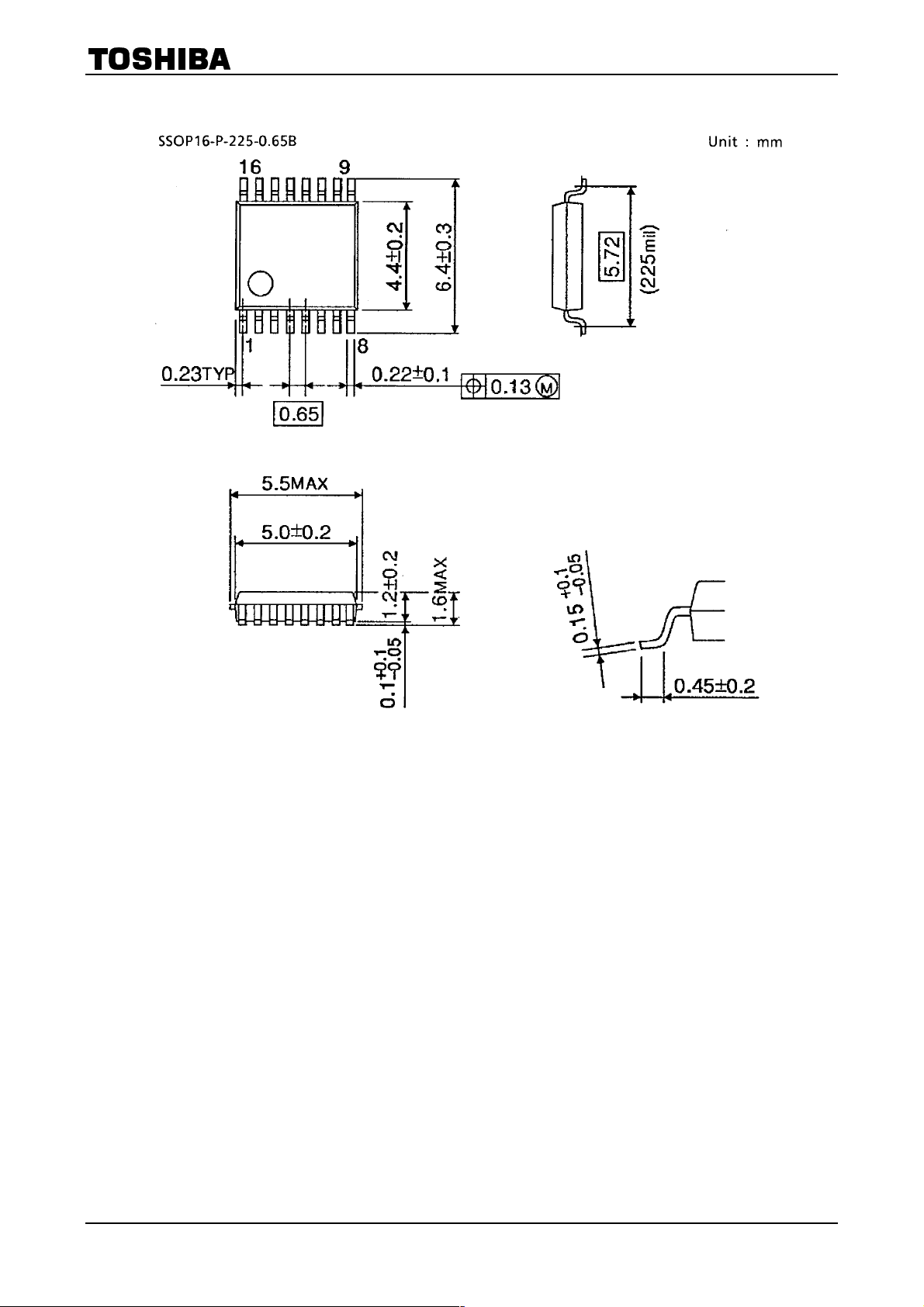
Package Dimensions
TB6552FN/FL
Weight: 0.07 g (typ.)
10
2002-09-11

Package Dimensions
TB6552FN/FL
Weight: 0.05 g (typ.)
11
2002-09-11

TB6552FN/FL
A
RESTRICTIONS ON PRODUCT USE
· TOSHIBA is continually working to improve the quality and reliability of its products. Nevertheless, semiconductor
devices in general can malfunction or fail due to their inherent electrical sensitivity and vulnerability to physical
stress. It is the responsibility of the buyer, when utilizing TOSHIBA products, to comply with the standards of
safety in making a safe design for the entire system, and to avoid situations in which a malfunction or failure of
such TOSHIBA products could cause loss of human life, bodily injury or damage to property.
In developing your designs, please ensure that TOSHIBA products are used within specified operating ranges as
set forth in the most recent TOSHIBA products specifications. Also, please keep in mind the precautions and
conditions set forth in the “Handling Guide for Semiconductor Devices,” or “TOSHIBA Semiconductor Reliability
Handbook” etc..
· The TOSHIBA products listed in this document are intended for usage in general electronics applications
(computer, personal equipment, office equipment, measuring equipment, industrial robotics, domestic appliances,
etc.). These TOSHIBA products are neither intended nor warranted for usage in equipment that requires
extraordinarily high quality and/or reliability or a malfunction or failure of which may cause loss of human life or
bodily injury (“Unintended Usage”). Unintended Usage include atomic energy control instruments, airplane or
spaceship instruments, transportation instruments, traffic signal instruments, combustion control instruments,
medical instruments, all types of safety devices, etc.. Unintended Usage of TOSHIBA products listed in this
document shall be made at the customer’s own risk.
· The products described in this document are subject to the foreign exchange and foreign trade laws.
· The information contained herein is presented only as a guide for the applications of our products. No
responsibility is assumed by TOSHIBA CORPORATION for any infringements of intellectual property or other
rights of the third parties which may result from its use. No license is granted by implication or otherwise under
any intellectual property or other rights of TOSHIBA CORPORATION or others.
000707EB
· The information contained herein is subject to change without notice.
12
2002-09-11

WWW.ALLDATASHEET.COM
Copyright ⓒ Each Manufacturing Company.
All Datasheets cannot be modified without permission.
ㅤ
This datasheet has been download from :
www.AllDataSheet.com
ㅤ
100% Free DataSheet Search Site.
Free Download.
No Register.
Fast Search System.
www.AllDataSheet.com
ㅤ
 Loading...