

查询TB6537供应商
TOSHIBA CMOS Integrated Circuit Silicon Monolithic
TB6537P,TB6537F
3-Phase Full-Wave Sensorless Controller for Brushless DC Motors
TB6537P/F is a 3-phase full-wave sensorless controller for
brushless DC motors. It is capable of controlling voltage by PWM
signal input. When combined with various drive circuits it can be
used for various types of motors.
Features
· 3-phase full-wave sensorless drive
· PWM control (PWM signal is supplied from external sources.)
· Turn-on signal output current: 20 mA
· Overcurrent protection function
· Forward/reverse modes
· Lead angle control function (0, 7.5, 15 and 30 degrees)
· Built-in lap turn-on function
· Two types of PWM output (upper PWM and upper/lower
alternate PWM)
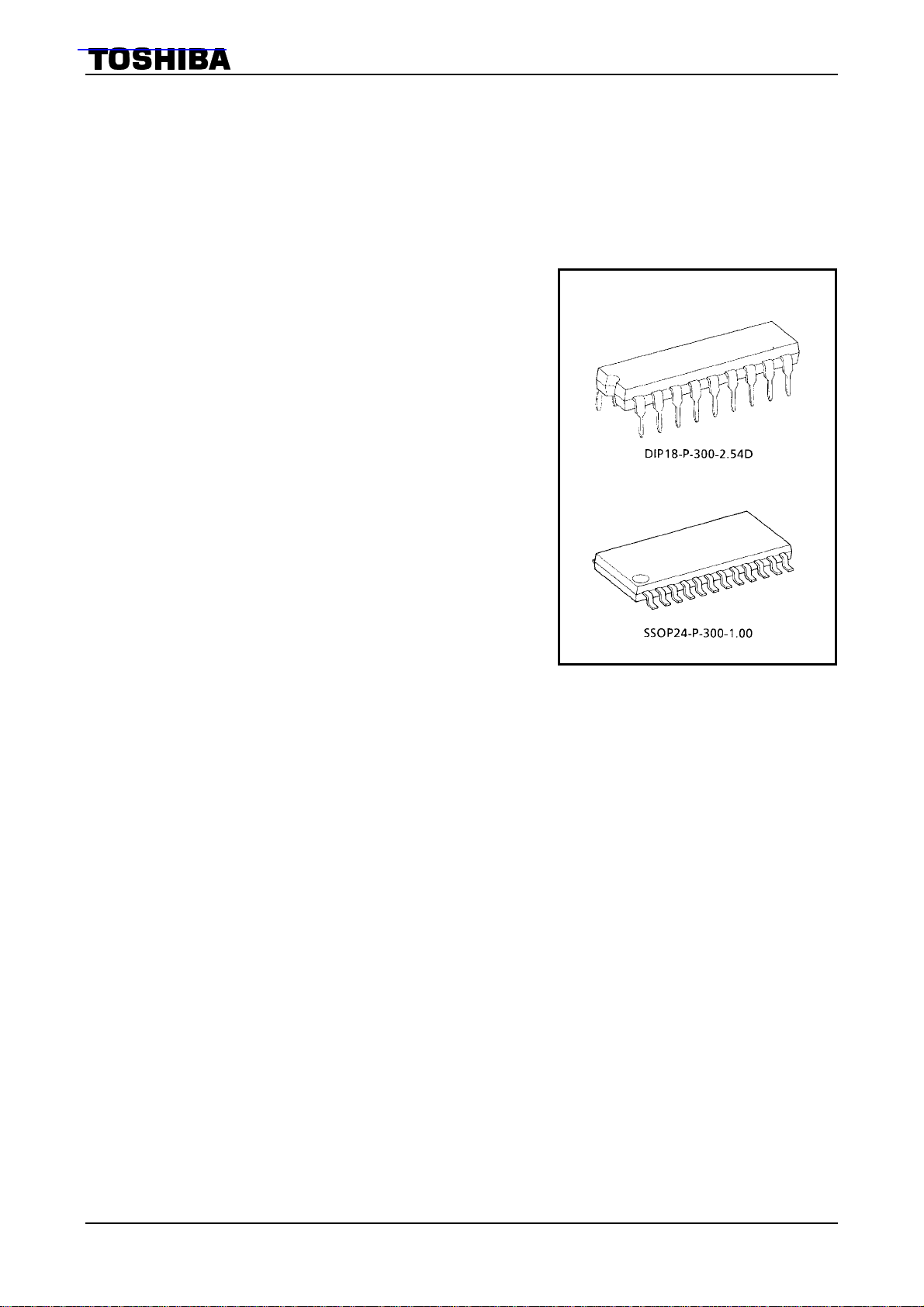
TB6537P
TB6537F
TB6537P/F
Weight
DIP18-P-300-2.54D: 1.47 g (typ.)
SSOP24-P-300-1.00: 0.32 g (typ.)
1
2003-02-20
Block Diagram
V
DD
10/13
TB6537P/F
PWM
SEL_OUT
SEL_LAP
CW_CCW
LA0
LA1
3/3
5/6
6/8
4/4
1/1
2/2
PWM Control
Rotation
Instruction
Circuit
Lead Angle
Setting Circuit
Clock
Generator
Circuit
Timing
Control
Turn-on Signal
Forming Circuit
Overcurrent
Protection
Circuit
Position
Detection
Circuit
11/14
13/17
15/21
12/15
14/19
16/22
17/23
18/24
OUT_UP
OUT_VP
OUT_WP
OUT_UN
OUT_VN
OUT_WN
OC
WAVE
7/10 8/11 9/12
Tin
XT
GND X
TB6537P/TB6537F
2
2003-02-20
Pin Assignment
TB6537P
TB6537P/F
TB6537F
LA0
LA1
PWM
CW_CCW
SEL_OUT
SEL_LAP
X
X
Tin
GND
1
2
3
4
5
6
7
T
8
9
18
17
16
15
14
13
12
11
10
WAVE
OC
OUT_WN
OUT_WP
OUT_VN
OUT_VP
OUT_UN
OUT_UP
V
DD
LA0
LA1
PWM
CW_CCW
NC
SEL_OUT
NC
SEL_LAP
NC
X
X
Tin
GND
1
2
3
4
5
6
7
8
9
10
T
11
12
24
23
22
21
20
19
18
17
16
15
14
13
WAVE
OC
OUT_WN
OUT_WP
NC
OUT_VN
NC
OUT_VP
NC
OUT_UN
OUT_UP
V
DD
3
2003-02-20
Pin Description
TB6537P/F
Pin No.
TB6537P TB6537F
1 1 LA0 I
2 2 LA1 I
3 3 PWM I
4 4 CW_CCW I
¾ 5 NC ¾ Not connected
5 6 SEL_OUT I
¾ 7 NC ¾ Not connected
6 8 SEL_LAP I
¾ 9 NC ¾ Not connected
7 10 X
8 11 X
9 12 GND ¾ Connected to GND.
10 13 V
11 14 OUT_UP O
12 15 OUT_UN O
¾ 16 NC ¾ Not connected
13 17 OUT_VP O
¾ 18 NC ¾ Not connected
14 19 OUT_VN O
Symbol I/O Description
Lead angle setting signal input pin
· LA0 = Low, LA1 = Low: Lead angle 0 degree
· LA0 = High, LA1 = Low: Lead angle 7.5 degree
· LA0 = Low, LA1 = High: Lead angle 15 degree
· LA0 = High, LA1 = High: Lead angle 30 degree
· B ui l t-in pull-down resistor
PWM signal input pin
· I nputs Low-acti ve PW M signal
· B ui l t-in pull-up resistor
· Disables input of duty-100% (Low) signal
High for 250 ns or longer is required.
Rotation direction signal input pin
· High: Reverse (U ® W ® V)
· Low, Open: Forward (U ® V ® W)
· B ui l t-in pull-down resistor
Pin to select the synthesis method of burn-in signal and PWM signal
· Low: Upper
· High: Upper/Lower alternate PWM
· B ui l t-in pull-down resistor
Lap turn-on select pin
· Low: Lap turn-on
· High: 120 degrees turn-on
· B ui l t-in pull-up resistor
¾
T
Tin
DD
Resonator connecting pin
· S el ects starting commutation frequency.
¾
¾ Connected to 5-V power supply.
Starting commutation frequency f
U-phase upper turn-on signal output pin
· U-phas e winding wire posit i ve ON/OFF switching pin
· ON: Low, OFF: High
U-phase lower turn-on signal output pin
· U-phas e winding wire negative ON/OFF switc hi ng pin
· ON: Hi gh, OFF: Low
V-phase upper turn-on signal output pin
· V-phase winding wire positive ON/OFF switching pin
· ON: Low, OFF: High
V-phase lower turn-on signal output pin
· V-phase winding wire negative ON/OFF switching pin
· ON: Hi gh, OFF: Low
PWM
= Resonator frequency fxt/(6 ´ 217)
st
4
2003-02-20
TB6537P/F
Pin No.
TB6537P TB6537F
¾ 20 NC ¾ Not connected
15 21 OUT_WP O
16 22 OUT_WN O
17 23 OC I
18 24 WAVE I
Symbol I/O Description
W-phase upper turn-on signal output pin
· W-phase winding wire positive ON/OFF switching
· ON: Low, OFF: High
W-phase lower turn-on signal output pin
· W-phase winding wire negative ON/OFF switching pin
· ON: Hi gh, OFF: Low
Overcurrent signal input pin
· High on this pin can put constraints on the turn-on signal which is performing PWM
· B ui l t-in pull-up resistor
Positional signal input pin
· Inputs majority logic synthesis signal of three-phase pin voltage.
· B ui l t-in pull-up resistor
Functional Description
1. Sensorless Drive
On receipt of PWM signal start instruction turn-in signal for forcible commutation (commutation
irrespective of the motor’s rotor position) is output and the motor starts to rotate. The motor’s rotation
causes induced voltage on winding wire pin for each phase.
When signals indicating positive or negative for pin voltage (including induced voltage) for each phase
are input on respective positional signal input pin, the turn-on signal for forcible commutation is
automatically switched to turn-on signal for positional signal (induced voltage).
Thereafter turn-on signal is formed according to the induced voltage contained in the pin voltage so as to
drive the brushless DC motor.
2. Starting commutation frequency
The forcible commutation frequency at the time of start is determined by the resonator’s frequency and
the number of counter bit (within the IC).
Starting commutation frequency f
The forcible commutation frequency at the time of start can be adjusted using inertia of the motor and
load.
· The forcible commutation frequency should be set higher as the number of magnetic poles increases.
· The forcible commutation frequency should be set lower as the inertia of the load increases.
3. PWM Control
PWM signal can be reflected in turn-on signal by supplying PWM signal from external sources.
The frequency of the PWM signal shoud be set adequately high with regard to the electrical frequency of
the motor and in accordance to the switching characteristics of the drive circuit.
Because positional detection is performed in synchronization with the rising edges of PWM signal,
positional detection cannot be performed with 0% duty or 100% duty.
control.
(resonator pin and counter bit select pin)
= Resonator frequency fxt/(6 ´ 2
st
(bit + 3)
pin
) bit = 14
Duty (max)
250 ns
Duty (min)
250 ns
The voltage applied to the motor is duty 100% because of the storage time of the drive circuit even if the
duty is 99%.
5
2003-02-20

4. Selecting PWM Output Form
PWM output form can be selected using SEL_OUT.
SEL_OUT ==== Low
Upper turn-on
signal
Lower turn-on
signal
Output voltage
SEL_OUT ==== High
Upper turn-on
signal
TB6537P/F
Lower turn-on
signal
Output voltage
6
2003-02-20
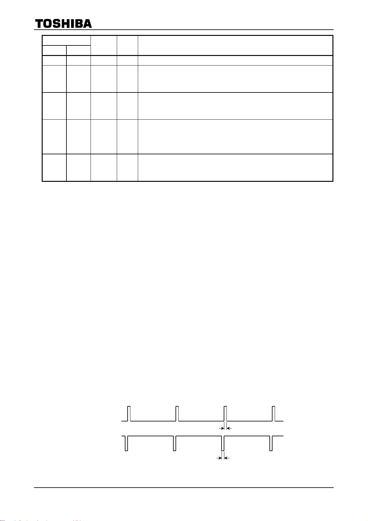
5. Positional Variation
Since positional detection is performed in synchronization with PWM signal, positional variation occurs
in connection with the frequency of PWM signal. Be especially careful when the IC is used for high-speed
motors.
PWM signal
TB6537P/F
Pin voltage
Reference voltage
Positional signal
Ideal detection timing Actual detection timing
Variation is calculated by detecting at two consecutive rising edges of PWM signal.
1/f
< Detection time variation < 2/f
p
6. Overcurrent protection function
An active phase which controls PWM is turned off by the rising-edge of the OC signal. The inactive phase
is turned on by the timing of the next PWM signal.
Pin voltage
p
fp: PWM frequency
7
2003-02-20

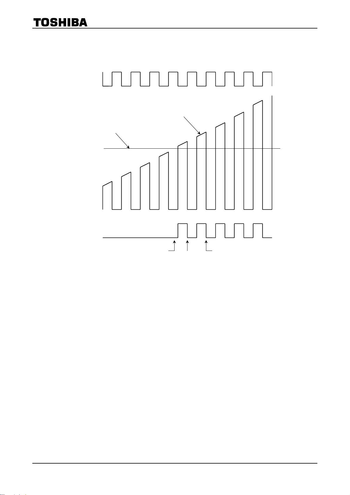
7. Lead Angle Control
_
_
_
_
_
_
_
_
_
_
_
_
_
_
_
The lead angle is 0 degree during the starting forcible commutation and when normal commutation is
started, automatically changes to the lead angle which has been set using LA0 and LA1. However, if both
LA0 and LA1 are set for High, the lead angle is 30 degrees in the starting forcible commutation as well as
in normal commutation.
Induced voltage
Turn-on signal
(1) Lead angle: 0 degree
OUT_UP
OUT_UN
VP
OUT
VN
OUT
OUT_WP
OUT_WN
(2) Lead angle: 7.5 degrees
(3) Lead angle: 15 degree
(4) Lead angle: 30 degree
OUT_UP
UN
OUT
OUT_VP
OUT_VN
OUT_WP
OUT_WN
OUT_UP
OUT_UN
OUT_VP
OUT_VN
WP
OUT
WN
OUT
OUT_UP
OUT_UN
VP
OUT
VN
OUT
OUT_WP
OUT_WN
8. Lap Turn-on Control
When SEL_LAP = High, the turn-on degree is 120 degrees. When SEL_LAP = Low, Lap Turn-on Mode
starts.
In Lap Turn-on Mode, the time between zero-cross point and the 120 degrees turn-on timing becomes
longer (shaded area in the below chart) so as to create some overlap when switching turn on signals. The
lap time differs depending ong the lead angle setting.
Induced voltage
Turn-on signal
(1) Lead angle: 0 degree
OUT_UP
OUT_UN
OUT_VP
OUT_VN
WP
OUT
WN
OUT
(2) Lead angle: 7.5 degrees
(3) Lead angle: 15 degree
(4) Lead angle: 30 degree
OUT_UP
OUT_UN
VP
OUT
VN
OUT
OUT_WP
OUT_WN
UP
OUT
UN
OUT
OUT_VP
OUT_VN
OUT_WP
OUT_WN
OUT_UP
OUT_UN
OUT_VP
OUT_VN
WP
OUT
WN
OUT
30 degrees
22.5 degrees
15 degrees
UV
UV
TB6537P/F
W
W
8
2003-02-20

9. Start/Stop Control
Start/Stop is controlled using PWM signal input pin.
A stop is acknowledged when PWM signal duty is 0, and a start is acknowledged when ON-signal of a
frequency 4 times higher than the resonator frequency or even higher is input continuously.
Timing chart
PWM signal
Detection
timing
Start
TB6537P/F
512 periods at the resonator frequency
PWM signal
Detection
timing
Stop
512 periods at the resonator frequency
Note: Take sufficient care for noise on PWM signal input pin.
First detection
First detection
Second detection Start
Second detection
and stop
9
2003-02-20

TB6537P/F
Maximum Ratings
Characteristics Symbol Rating Unit
Power supply voltage V
Input voltage V
Turn-on signal output current I
Power dissipation PD
Operating temperature T
Storage temperature T
(Ta ==== 25°C)
DD
in
OUT
opr
stg
Recommended Operating Conditions
Characteristics
Power supply voltage V
Input voltage V
PWM frequency f
Oscillation frequency f
Symbol Test Condition Min Typ. Max Unit
DD
in
PWM
osc
5.5 V
-0.3 to VDD + 0.3 V
20 mA
TB6537P 1.25
TB6537F 0.59
-30 to 85 °C
-55 to 150 °C
W
(Ta ==== ----30 to 85°C)
¾ 4.5 5.0 5.5 V
¾ -0.3 ¾
¾ ¾ 16 ¾ kHz
¾ 1.0 ¾ 10 MHz
V
DD
+ 0.3
V
10
2003-02-20

TB6537P/F
Electrical Characteristics
Characteristics
Static power supply current I
Dynamic power supply current I
Input current
Input voltage
Input hysteresis voltage V
Output voltage
Output leak current
Output delay time
(Ta ==== 25°C, VDD ==== 5 V)
Symbol
DD
DD (opr)
I
(H) ¾
IN-1
I
(L) ¾
IN-1
I
(H) ¾
IN-2
I
(L) ¾
IN-2
VIN (H) ¾
(L) ¾
V
IN
H
V
(H) ¾
O-1
V
(L) ¾
O-1
V
(H) ¾
O-2
V
(L) ¾
O-2
IL (H) ¾
I
(L) ¾
L
t
pLH
t
pHL
Test
Circuit
¾ PWM = H, X
¾ PWM = 50% Duty, X
= 5 V, PWM, OC, WAVE_U,
V
IN
SEL_LAP
= 0 V, PWM, OC, WAVE_U,
V
IN
SEL_LAP
= 5 V, CW_CCW, LA0, LA1,
V
IN
SEL_OUT
= 0 V, CW_CCW, LA0, LA1,
V
IN
SEL_OUT
PWM, OC, SEL_LAP, CW_CCW
WAVE_U, LA0, LA1, SEL_OUT
PWM, OC, SEL_LAP, CW_CCW
WAVE_U, LA0, LA1, SEL_OUT
PWM, OC, SEL_LAP, CW_CCW
¾
WAVE_U, LA0, LA1, SEL_OUT
I
= -1 mA
OH
OUT_UP, OUT_VP, OUT_WP
I
= 20 mA
OH
OUT_UP, OUT_VP, OUT_WP
I
= -20 mA
OH
OUT_UN, OUT_VN, OUT_WN
I
= 1 mA
OH
OUT_UN, OUT_VN, OUT_WN
V
= 5.5 V, V
DD
OUT_UP, OUT_VP, OUT_WP
OUT_UN, OUT_VN, OUT_WN
V
= 5.5 V, V
DD
OUT_UP, OUT_VP, OUT_WP
OUT_UN, OUT_VN, OUT_WN
¾ PWM-Output
Test Condition Min Typ. Max Unit
= H ¾ 0.1 0.3 mA
Tin
= 4 MHz ¾ 1 3 mA
Tin
¾ 0 1
-75 -50 ¾
mA
¾ 50 75
-1 0 ¾
3.5 ¾ 5
V
GND ¾ 1.5
¾ 0.6 ¾ V
OUT
OUT
4.3 ¾ V
GND ¾ 0.5
4.0 ¾ V
GND ¾ 0.5
= 0 V
¾ 0 10
= 5.5 V
¾ 0 10
¾ 0.5 1
¾ 0.5 1
DD
V
DD
mA
ms
11
2003-02-20
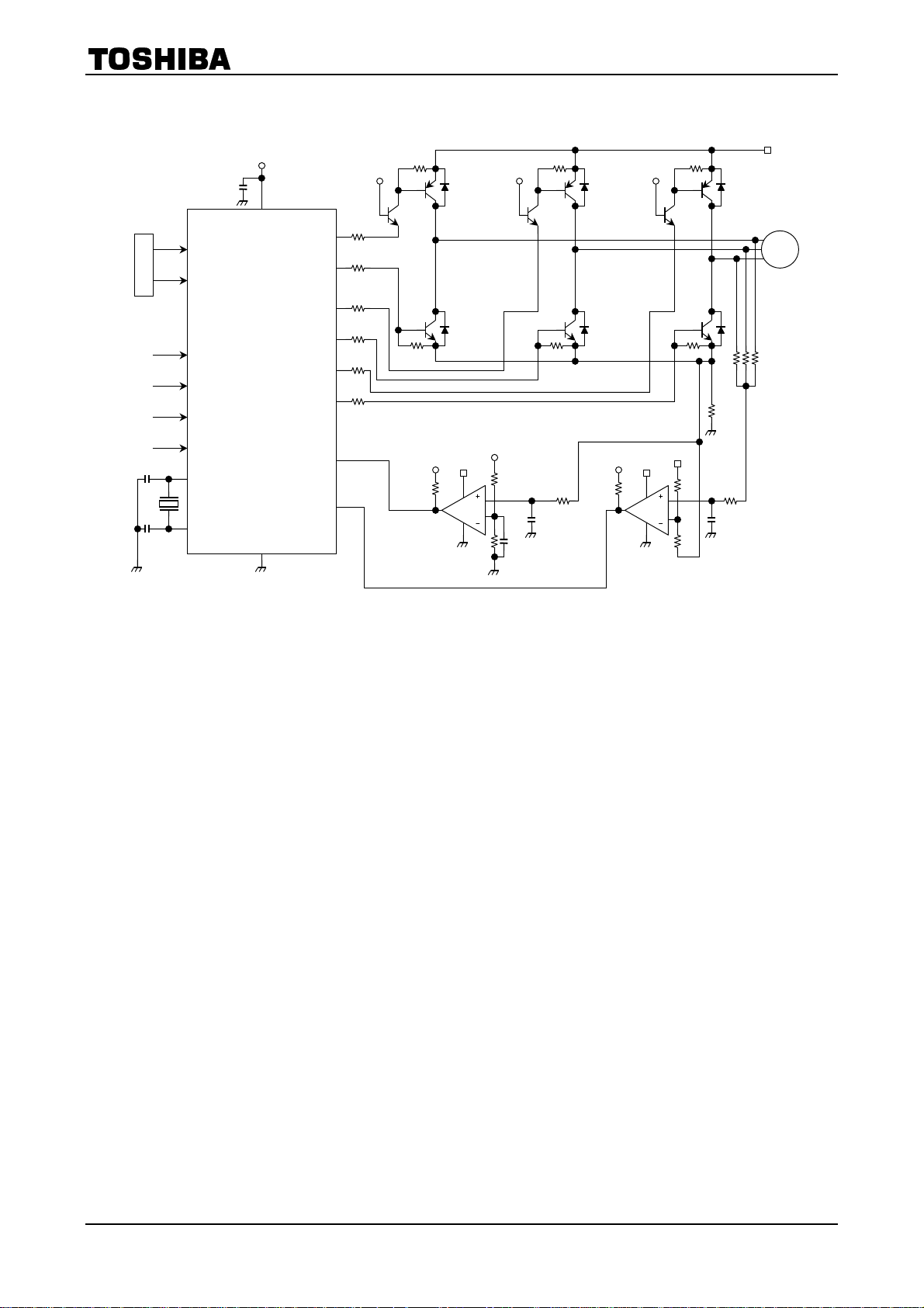
Application Circuit Example
X
X
5 V
V
DD
OUT_UP
OUT_UN
OUT_VP
OUT_VN
OUT_WP
OUT_WN
TB6537F/P
H/L
H/L
H/L
CPU
PWM
CW_CCW
LA0
LA1
SEL_OUT
TB6537P/F
V
M
100 kW ´ 3
1 W 22 pF
H/L
4 MHz
SEL_LAP
T
Tin
GND
OC
WAVE
10 kW
TA75393P
3 kW
1 kW
0.01 mF
0.01 mF
200 W
10 kW
TA75393P
1 kW
100 kW 100 kW
Note 1: Take enough care in designing output VDD line and GND line to avoid short circuit between outputs, VDD
fault or GND fault which may cause the IC to break down.
Note 2: The above application circuit and values mentioned are just an example for reference. Since the values may
vary depending on the motor to be used, appropriate values must be determined through experiments before
using the device.
12
2003-02-20
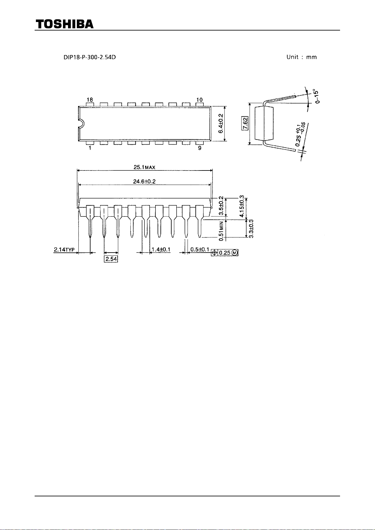
Package Dimensions
TB6537P/F
Weight: 1.47 (typ.)
13
2003-02-20

Package Dimensions
TB6537P/F
Weight: 0.32 (typ.)
14
2003-02-20

TB6537P/F
A
RESTRICTIONS ON PRODUCT USE
· TOSHIBA is continually working to improve the quality and reliability of its products. Nevertheless, semiconductor
devices in general can malfunction or fail due to their inherent electrical sensitivity and vulnerability to physical
stress. It is the responsibility of the buyer, when utilizing TOSHIBA products, to comply with the standards of
safety in making a safe design for the entire system, and to avoid situations in which a malfunction or failure of
such TOSHIBA products could cause loss of human life, bodily injury or damage to property.
In developing your designs, please ensure that TOSHIBA products are used within specified operating ranges as
set forth in the most recent TOSHIBA products specifications. Also, please keep in mind the precautions and
conditions set forth in the “Handling Guide for Semiconductor Devices,” or “TOSHIBA Semiconductor Reliability
Handbook” etc..
· The TOSHIBA products listed in this document are intended for usage in general electronics applications
(computer, personal equipment, office equipment, measuring equipment, industrial robotics, domestic appliances,
etc.). These TOSHIBA products are neither intended nor warranted for usage in equipment that requires
extraordinarily high quality and/or reliability or a malfunction or failure of which may cause loss of human life or
bodily injury (“Unintended Usage”). Unintended Usage include atomic energy control instruments, airplane or
spaceship instruments, transportation instruments, traffic signal instruments, combustion control instruments,
medical instruments, all types of safety devices, etc.. Unintended Usage of TOSHIBA products listed in this
document shall be made at the customer’s own risk.
· The products described in this document are subject to the foreign exchange and foreign trade laws.
· The information contained herein is presented only as a guide for the applications of our products. No
responsibility is assumed by TOSHIBA CORPORATION for any infringements of intellectual property or other
rights of the third parties which may result from its use. No license is granted by implication or otherwise under
any intellectual property or other rights of TOSHIBA CORPORATION or others.
000707EB
· The information contained herein is subject to change without notice.
15
2003-02-20
 Loading...