TOSHIBA TB62732FU Technical data

查询TB62732FU供应商
TOSHIBA
TOSHIBA BiCD DIG I TAL INTEGRATED CIRCUIT SIL IC ON M ON OL I THIC
T B 6 2 7 3 2 F U
The step up type DC-DC converter only for white LED driver lighting
FEATURE
The TB62732FU is a LED driver by the high efficienc y
step up type DC-DC converter that 2-4 serial white LED
can be turned on.
This IC builds in the NchMOS FET transistor to switch
the coil, and builds in the function which derate
the LED current co rresponding to the rise in temperature.
And, the average LED current can be set up easily
by the resistance with the outside.
This IC is the most suitable as a driver
of the LED liquid cr ysta back ligh t of the PDA,
the cellular phone and the t he handy terminal.
T B 6 2 7 3 2 F U
T B 6 2 7 3 2 F U
CHARACTERISTICS
*Maximum output voltage Vo =< 17V
*The variable setup of the average LED current value by
the resistance w ith the outside.
18 mA (typ) @ R_sens = 2.7 ohms
20 mA (typ) @ R_sens = 2.4 ohms
*Supply electric power
It is turned on to the 320 mW load.
*Compact package
SSOP6 - P - 0.95B ( SOT23-6pin )
*The LED current der ating function is built in.
The derating of LED current vs set temperature,
on the automatic operation.
*High efficie n cy
80% of the efficiency. @ 2-3LEDs turn on. IF=20mA (typ) )
Ron=2.0 ohms (standard) @ Vin = 3.0 - 5.5V
The power MOS transistor building in of low Ron.
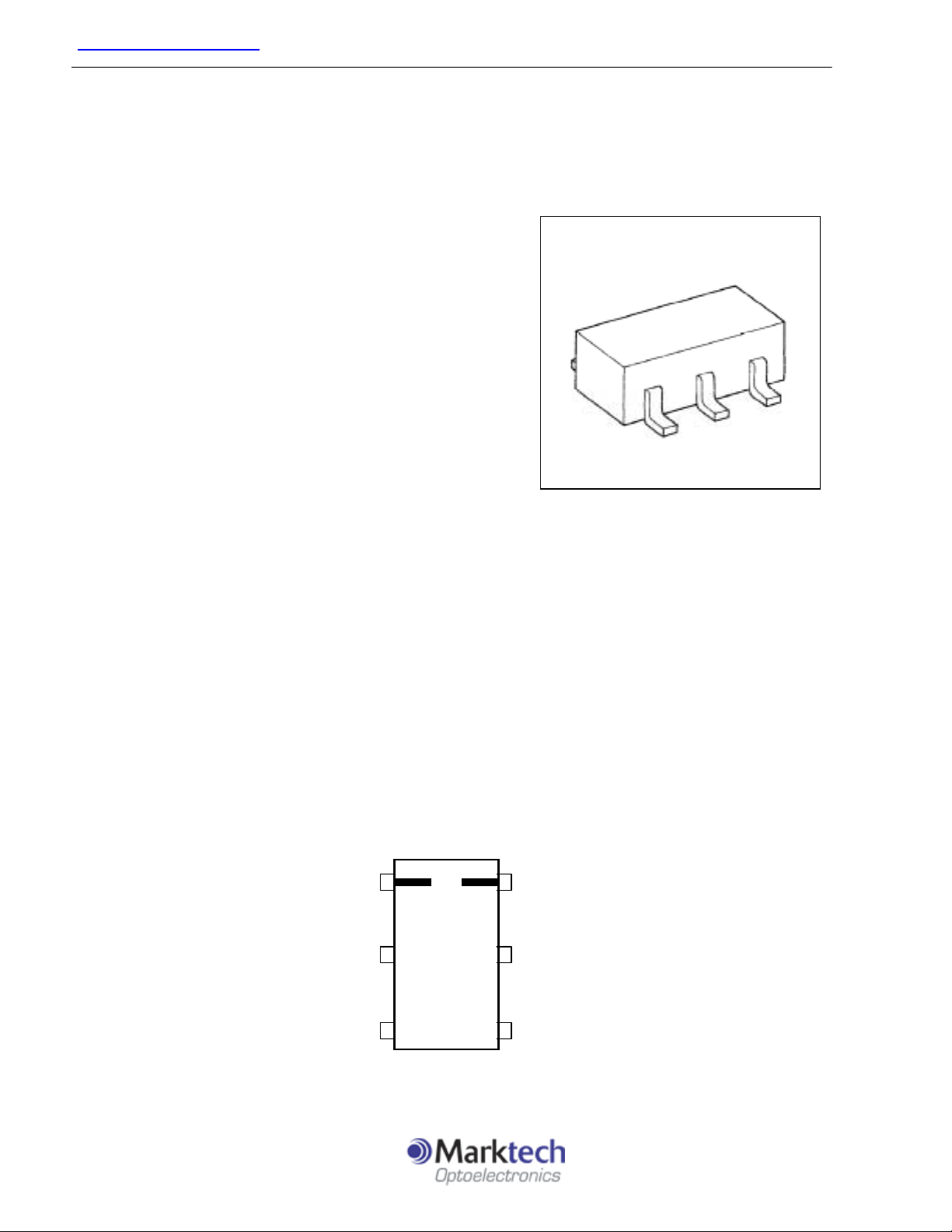
*Pin assignment ( Top View)
K
V
A
SSOP6-P-0.95B
Weight: 0.016 g (ty p )
GND
SHDN
GND
VCC
Note 1:
Be careful of handling because there is a terminal which is poor at ESD in this product.
Company Headquarters
Company Headquarters
3 Northway Lane North
3 Northway Lane North
Latham, New York 12110
Latham, New York 12110
Toll Free: 800.984.5337
Toll Free: 800.984.5337
Fax: 518.785.4725 Web: www.marktechopto.com | Email: info@marktechopto.com
Fax: 518.785.4725 Web: www.marktechopto.com | Email: info@marktechopto.com
California Sales Office:
950 South Coast Drive, Suite 265
950 South Coast Drive, Suite 265
California Sales Office:
Costa Mesa, California 92626
Costa Mesa, California 92626
Toll Free: 800.984.5337
Toll Free: 800.984.5337
Fax: 714.850.9314
Fax: 714.850.9314

TOSHIBA
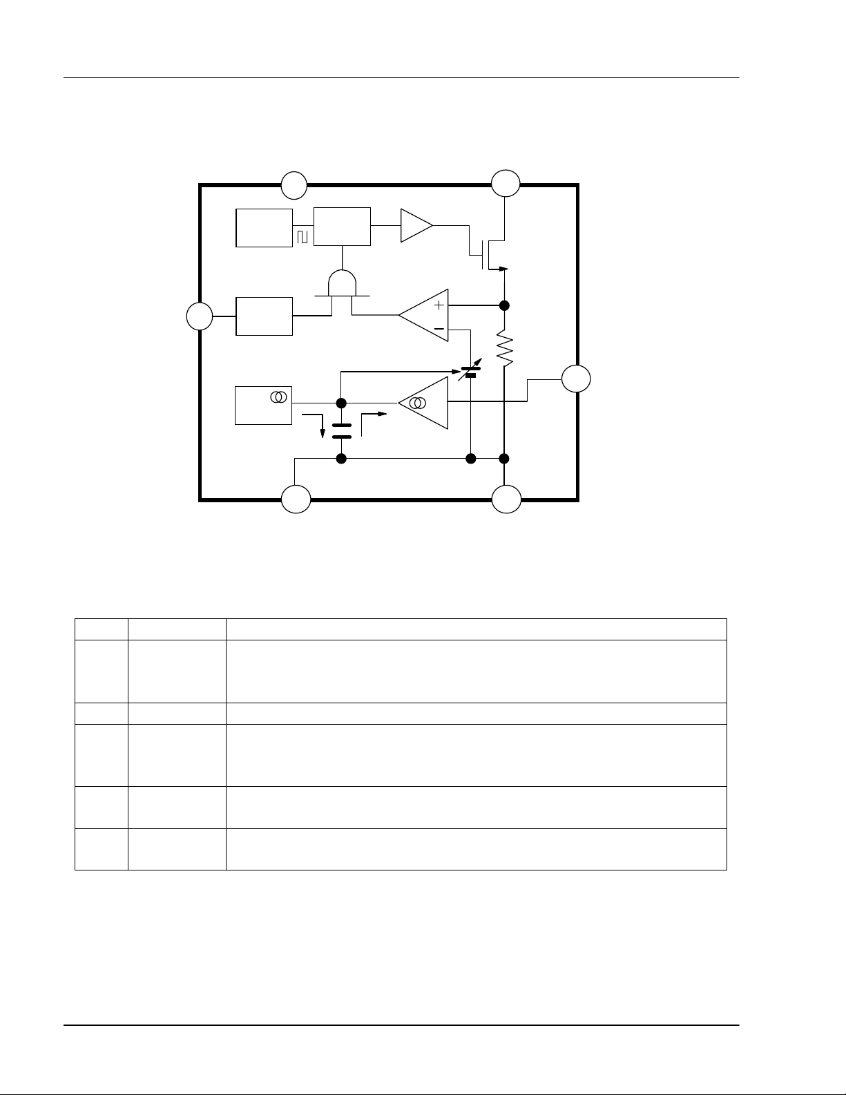
BLOCK DIAGRAM
T B 6 2 7 3 2 F U
SHDN
Vcc
1.0MHz
OSC
STB
REF
i(add)
GND
A
Buffer
Q
S
R
0.35
0 - 0.12V
K
A
i(sub)
GND
FIg 1 : BLOCK DIAGRAM
TERMINAL EXPLANATION
No
1 K
2, 5 GND It is the ground term inal of the logic part.
3 SHDN
4 Vcc
6 A
Note 2 : Connect all the GND terminals to the ground electric potencia l.
Name Function expl anation
It is the connection terminal with cathode and IF setup resistance of
LED. It is the feedback terminal of the charge voltage wave form for the
LED current control.
It is the enable termi nal. It becomes the standby mode with "L", and the
LED is turned off. The lighting operati on is given with "H".
It is the input termin al of the operation voltage for the IC. The operating
voltage is 3.0 to 5. 5V.
It is the swit ch terminal of the coil for the D C/DC converter . The switch is
a Nch MOSFET transistor . T his is low Ron.
2
27, Feb 2002 (Ver.04)

TOSHIBA
ABSOLUTE MAXIMUM RATING ( unless other wised notice Topr = 25 degr ee )
Characteristics
Supply voltage Vcc - 0.3 to + 6.0 V
Input voltage Vin - 0.3 to VCC + 0.3
A(anode) terminal
current
A(anode) terminal
voltage
Power dissipation Pd 0.41 ( not on PCB ) W
Saturation heat
resistance
Operation
temperature
Storage
temperature
Maximum juction
temperature
Symbol Rating Unit
Io(A) + 380 mA
Vo(A) - 0.3 to + 17 V
0.47 (on PCB) *Note 3
Rth(j-a)1 300 ( not on PCB ) degree/W
Rth(j-a)2 260 ( onPCB )
Topr - 40 to + 85
Tstg - 40 to + 150 degree
Tj 125
T B 6 2 7 3 2 F U
Note 3 : When every time the ambient temperature gets over 25 degrees with 1 degree, the
allowable loss must reduce 3.8mW/degree more than maximum rated value. ( When on PCB.)
RECOMMENDED OPERATION COND ITION (unless otherwise notice Topr = -40 to 85 degree)
Characeristics
Supply voltage Vcc - 3.0 - 4.3 V
SHDN terminal
H-level input
voltage
SHDN terminal
L-level input voltage
SHDN terminal
"H"level input pulse
width
Symbol Test condition min typ max Unit
VIH -
VIL - 0 - 0.5
tpw SHDN - 0.5 - - ms
Vcc
-0.5
- Vcc V
Setup LED current
(mean)
Io
Maximum step up condit ion.
Vo (A) is change from 3V to
16V
3
5 - 20 mA
27, Feb 2002 (Ver.04)

TOSHIBA
ELECTRIC CHAR ACTERISTICS
( unless otherwised notice, Topr = -40 to 85 degree & Vcc = 3.0 to 5.5 V)
Characteristics
Supply voltage Vcc 3.0 - 5.5 V
Symbol Test condition min typ max Unit
T B 6 2 7 3 2 F U
Operation supply
current
Stand-by supply
current
SHDN terminal
current
MOS-Tr on
resistance
MOS-Tr switching
frequency
A terminal voltag e Vo(A) 17 - - V
A terminal current Io(A) 320 350 380 mA
A terminal
leakage current
Set up LED
current (mean)
Icc(On) Vcc = 3.6V - 0.9 mA
Icc(SHDN) SHDN = 0 V - 0.5 1.2 uA
I_SHDN
Ron
fOSC 0.7 1.0 1.3 MHz
Ioz(A) - 0.5 1 uA
Io
built in pull-down resisance
detection resistance value is
SHDN = Vcc,
Io(A) <= 380 mA,
contained.
Vcc = 3 - 4.3V,
R_sens = 2.7 ohms,
- 4.2 7 uA
- 2.0 2.5 ohms
19.6 mA
LED current Vcc
dependence
Derating start
ambient
temperature
Note 4 : The derating function carries out the measurement in Ta= 25 degree not to work. The
specifications don't contain the dispersion of the R_Sens resistor. Io has the possibility to be different
from the specifications by the inductance value and the relations of the load.
Note 5 : It is a specifications guarantee by the design.
dIo
Tdel
Topr = 25 degree (Not e 4)
R_sens = 2.7 ohms, L = 10uH,
L = 6.8uH,
Vo = 16V (Note 5)
4
+/-5 +/-10 %
- 45 -
27, Feb 2002 (Ver.04)
degr
ee

TOSHIBA
T B 6 2 7 3 2 F U
Vcc
1.0 MHz
OSC
Vin
BASIC OPERATION
The step up type DC/DC converter is applied, and the basic circuit of the TB62732FU adopts peak control of
the current pulse.
SHDN
STB
C1
REF
i(add)
Fig 2 : the application circuit (example)
IL, ILpeak
6.8 uH
SQ
R
0 - 0.12V
i(sub)
Buffer
A
A
NMOS
0.35
GND
Ic2
K
R_sens
C2
Io
The internal MOS transistor NMOS is turned on in the fixed frequency fOSC =1MHz, and the charge has the
energy in the inductance.
Inductance electric current IL turns off NMOS when it reaches 80% of 1/1MHz when it
increased from IL = 0 and it reached IL = ILpeak = 380 (mA, typ).
The shot key diode is turned on, and IL = Ic2 flows, because the coil may keep IL = ILpeak.
After that, Ic2 is decrease, and become IL = 0.
This operation is repeated, and Ic2 is fully done as to the charge, and it becomes Io, and flows to LED.
The details of a basic pulse to use for the current control are shown in Fig 3.
Muximum duty 80 %
IL = IL peak
ILpeak=
When fitness inductance
IL becomes 0 in the time.
380(mA, max)
When Un-fitness inductance
IL doesn't become 0 in the time.
T = 1/fOSC, fOSC = 1MHz(typ)
Fig 3 : the switching wave form of the inductance
5
27, Feb 2002 (Ver.04)
 Loading...