


www.DataSheet4U.com
DataSheet4U.com
DataSheet4U.com
DataSheet4U.com
DataSheet4U.com
TB62706BNG/BFG
4
.com
U
DataSheet
TOSHIBA Bi-CMOS INTEGRATED CIRCUIT SILICON MONOLITHIC
TB62706BNG, TB62706BFG
16BIT SHIFT REGISTER, LATCHES & CONSTANT CURRENT DRIVERS
The TB62706BNG, TB62706BFG are specifically designed for LED
and LED DISPLAY constant current drivers.
This constant current output circuits are able to set up external
resistor (I
These devices are monolithic integrated circuit designed to be used
together with Bi-CMOS process.
The devices consist of 16bit shift register, latch, AND-GATE and
Constant Current Drivers.
These products are Pb free.
= 5~90 mA). (Note)
OUT
FEATURES
l Constant Current Output : Can set up all output current with
one resister for 5 to 90 mA.
l Maximum Clock Frequency : f
l 5 V C- MOS Compatible Input
l Package : SDIP24-P-300-1.78 (TB62706BNG)
SSOP24-P-300- 1.00B (TB62706BFG)
l Constant Output Current Matching:
OUTPUT-GND
VOLTAGE
=0.4 V ±6.0% 5~40 mA
=0.7 V ±6.0% 5~90 mA
CURRENT
MATCHING
= 15 (MHz) (Cascade
CLK
Connected Operate, T
OUTPUT
CURRENT
= 25°C)
opr
TB62706BNG
TB62706BFG
Weight
SDIP24-P-300-1.78 : 1.22 g (typ.)
SSOP24-P-300-1.00B : 0.32 g (typ.)
PIN CONNECTION
Company Headquarters
Company Headquarters
3 Northway Lane North
3 Northway Lane North
Latham, New York 12110
Latham, New York 12110
Toll Free: 800.984.5337
Toll Free: 800.984.5337
Fax: 518.785.4725 Web: www.marktechopto.com | Email: info@marktechopto.com
Fax: 518.785.4725 Web: www.marktechopto.com | Email: info@marktechopto.com
(Top view)
California Sales Office:
950 South Coast Drive, Suite 265
950 South Coast Drive, Suite 265
California Sales Office:
Costa Mesa, California 92626
Costa Mesa, California 92626
Toll Free: 800.984.5337
Toll Free: 800.984.5337
Fax: 714.850.9314
Fax: 714.850.9314
www.DataSheet4U.com
DataSheet4U.com
DataSheet4U.com
DataSheet4U.com
DataSheet4U.com
2
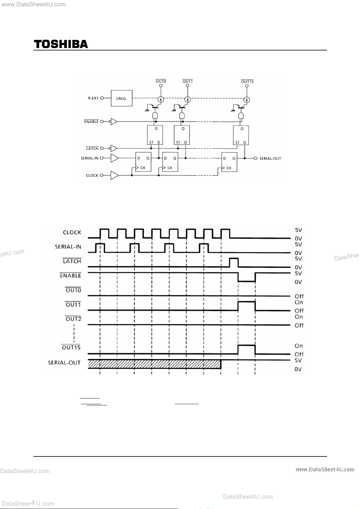
BLOCK DIAGRAM
4
.com
U
DataSheet
TIMING DIAGRAM
TB62706BNG/BFG
Note: Latches are level sensitive, not rising edges sensitive and not syncronus CLOCK.
Input of LATCH-terminal to H Level, data passes latches, and input to L level, data hold latches.
Input of ENABLE-terminal to H level, all output (OUT0~15) do off.
2004-06-24
www.DataSheet4U.com
DataSheet4U.com
DataSheet4U.com
DataSheet4U.com
DataSheet4U.com
3
TERMINAL DISCRIPTION
ENABLE
LATCH
4
.com
U
DataSheet
PIN No. PIN NAME FUNCTION
1 GND GND terminal for control logic.
2 SERIAL-IN Input terminal of a serial-data for shift-register.
3 CLOCK Input terminal of a clock for data shift to up-edge.
4 LATCH
5~20
21
22 SERIAL-OUT Output terminal of a serial-data for next SERIAL-IN terminal.
23 R-EXT Input terminal of connects with a resister for to set up all output current.
24 VDD 5 V Supply voltage terminal.
ENABLE
TRUTH TABLE
Input terminal of a data strobe. Latches passes data with “H” level input of
LATCH - terminal, and hold data with "L" level input.
Output terminals.
15~OUT0
Input terminal of output enable. All outputs (OUT0~15) do off with “H” level input of
ENABLE
TB62706BNG/BFG
- terminal, and do on with "L" level input.
CLOCK
UP H L Dn Dn ··· D
UP L L D
UP H L D
DOWN X L D
DOWN X H D
Note:
LATCH
= on in case of Dn = H level and
15~OUT0
ENABLE
SERIAL-IN
···
OUT0
No change D
n+1
D
n+2
D
n+3
Off D
n+3
··· D
n+2
··· D
n+2
= off in case of Dn = L level.
15~OUT0
OUT7
n-7
n-5
n-5
···
··· D
··· D
··· D
OUT15
D
n-15
D
n-13
D
n-13
A resistor is connected with R-EXT and GND accompanied with outside, and it is necessary that a correct power
supply voltage is supplied.
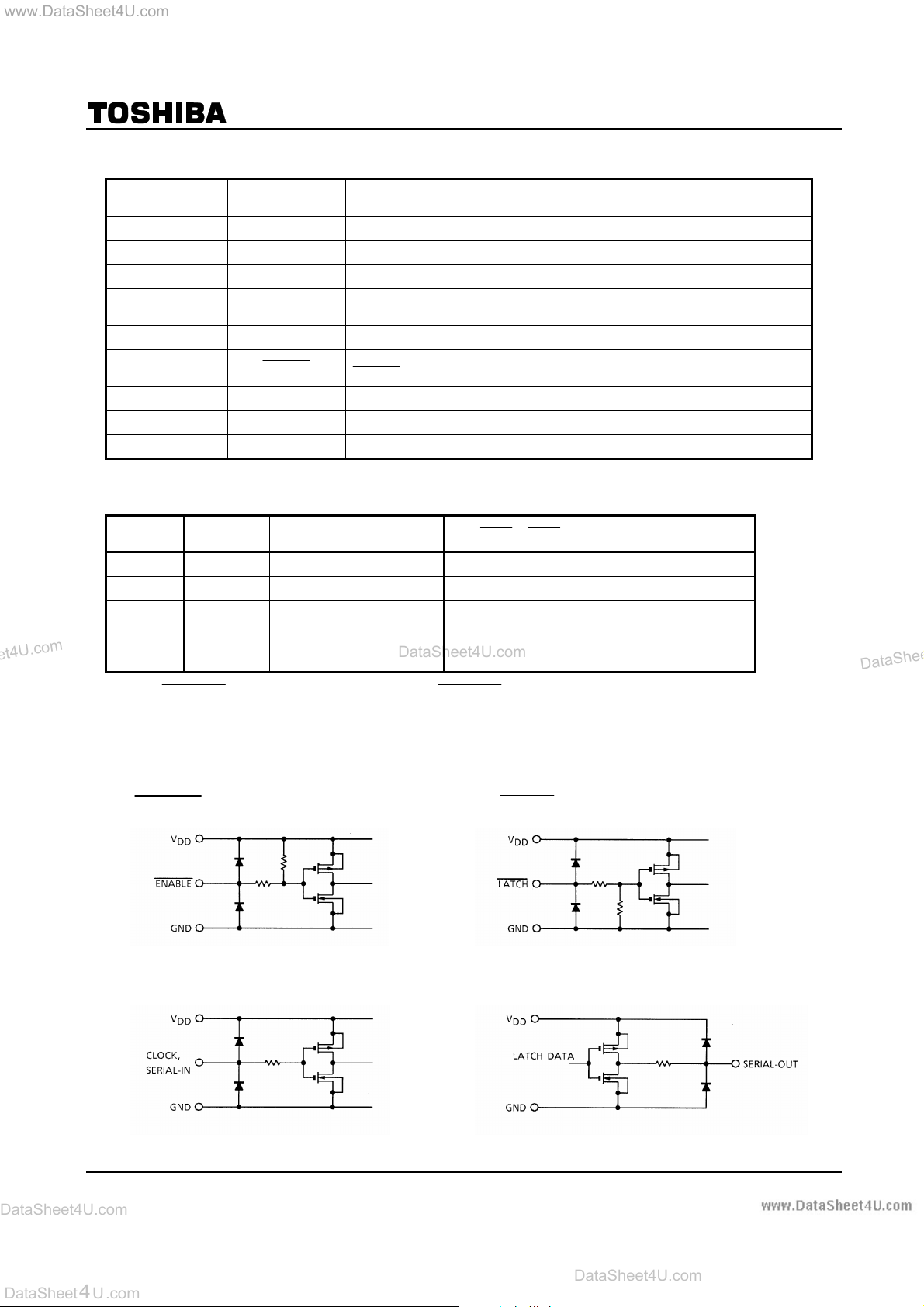
EQUIVALENT CIRCUIT OF INPUTS AND OUTPUTS
1.
3. CLOCK, SERIAL- IN terminal 4. SERIAL- OUT terminal
terminal 2.
terminal
SERIAL-OUT
n-15
n-14
n-13
n-13
n-13
2004-06-24
www.DataSheet4U.com
DataSheet4U.com
DataSheet4U.com
DataSheet4U.com
DataSheet4U.com
TB62706BNG/BFG
4
4
.com
U
DataSheet
MAXIMUM RATINGS
CHARACTERISTIC SYMBOL RATING UNIT
Supply Voltage VDD 0~7.0 V
Input Voltage VIN - 0.4~V
Output Current I
Output Voltage V
Clock Frequency fCK 15 MHz
GND Terminal Current I
Power Dissipation PD
Tharmal Resistance R
Operating Temperature T
Storage Temperature T
(Ta = 25°C)
+ 0.4 V
DD
90 mA
OUT
- 0.5~17.0 V
OUT
1440 mA
GND
1.78 (BNG- type : ON PCB, Ta = 25°C )
1.00 (BFG- type : ON PCB, Ta = 25°C )
th (j-a)
- 40~85 °C
opr
- 55~150 °C
stg
BNG : 70 (BN-type : ON PCB)
BFG : 120 (BF-type : ON PCB)
Note: BN-type : Ambient temperature delated above 25°C in the proportion of 14.2 mW / °C
BF-type : Ambient temperature delated above 25°C in the proportion of 8.3 mW / °C
RECOMMENDED OPERATING CONDITION
(Ta = - 40~85°C unless otherwise noted)
W
°C / W
CHARACTERISTIC SYMBOL CONDITION MIN TYP. MAX UNIT
Supply Voltage VDD – 4.5 5.0 5.5 V
Output Voltage V
Output Current
Input Voltage
Pulse Width
LATCH
CLOCK Pulse Width t
ENABLE
Set-Up Time for DATA t
Hold Time for DATA t
Set-Up Time for
Hold Time for
Clock Frequency f
Power Dissipation PD
Pulse Width
LATCH
LATCH
t
t
– – – 15.0
OUT
IO OUTn, DC 1 circuit 5 – 88
IOH SERIAL-OUT – – 1.0
IOL SERIAL-OUT – – - 1.0
VIH –
VIL – - 0.3
100
t
LATw
50 – – ns
w CLK
4500 – – ns
t
ENw
VDD = 4.5~5.5 V
60 – – ns
setup (D)
20 – – ns
hold (D)
100
setup (L)
hold (L)
Cascade operation – – 10.0 MHz
CLK
Ta = 85°C (BNG- type) – – 0.92
Ta = 85°C (BFG- type) – – 0.50
0.7
V
DD
60 – – ns
–
–
– – ns
– – ns
VDD
+0.3
0.3
V
DD
V
mA
V
W
2004-06-24
www.DataSheet4U.com
DataSheet4U.com
DataSheet4U.com
DataSheet4U.com
DataSheet4U.com
TB62706BNG/BFG
5
4
.com
U
DataSheet
ELECTRICAL CHARACTERISTICS
CHARACTERISTIC SYMBOL
"H" Level VIH – Ta = -40~85°C
Input Voltage
"L" Level VIL – Ta = -40~85°C GND –
Output Leakage Current IOH – VOH = 15.0 V – – 10 µA
Output Voltage SERIAL-OUT
Output Current 1
Current Skew ∆ I
Output Current 2
Current Skew ∆ I
Supply Voltage Regulation % / VDD –
Pull-Up Resistor R
Pull-Down Resistor R
"OFF"
Supply Current
"ON"
IN (down)
I
DD (off) 1
I
DD (off) 2
I
DD (off) 3
I
DD (on) 1
I
DD (on) 2
(VDD = 5.0 V, Ta = 25°C unless otherwise noted)
TEST
CIRCUIT
VOL – IOL = 1.0 mA – – 0.4
VOH – IOH = -1.0 mA 4.6 – –
I
– VCE = 0.7 V 34.1 40.0 45.9
OL1
I
– VCE = 0.4 V
OL2
–
OL1
I
– VCE = 1.0 V 64.2 75.5 86.8
OL3
I
– VCE = 0.7 V
OL4
–
OL2
– – 150 300 600
IN (up)
– – 100 200 400
–
– R
– R
– R
– R
IO = 40 mA,
VCE = 0.4 V
IO = 75 mA,
VCE = 0.7 V
R
Ta = -40~85°C
R
CONDITION MIN TYP. MAX UNIT
= 470 Ω,
EXT
= Open,
EXT
= 470 Ω,
EXT
= 250 Ω,
EXT
= 470 Ω,
EXT
= 250 Ω,
EXT
15~OUT0
= off
0.7
V
R
= 470 Ω
EXT
(Include current
matching)
R
= 470 Ω – ±1.5 ±6.0 %
EXT
R
= 250 Ω
EXT
(Include current
matching)
R
= 250 Ω – ±1.5 ±6.0 %
EXT
= off 3.5 5.8 8.0
15~OUT0
= off 6.5 10.7 15.0
15~OUT0
= on 10.0 16.0 22.0
15~OUT0
= on 18.0 28.3 38.5
15~OUT0
33.7 39.5 45.3
63.8 75.0 86.2
– V
DD
– 1.5 5.0 % / V
– 0.6 1.2
0.3
V
DD
DD
V
V
mA
mA
Ω
Ω
mA
2004-06-24

www.DataSheet4U.com
DataSheet4U.com
DataSheet4U.com
DataSheet4U.com
DataSheet4U.com
TB62706BNG/BFG
6
4
.com
U
DataSheet
SWITCHING CHARACTERISTICS
CHARACTERISTIC SYMBOL
CLK-
Propagation
Delay Time
(“L” to “H”)
Propagation
Delay Time
(“H” to “L”)
Pulse Width
Set-up Time
Hold Time
Maximum CLOCK Rise Time tr – – – 10 µs
Maximum CLOCK Fall Time tf – – – 10 µs
Output Rise Time tor – 150 300 600
Output Fall Time tof –
LATCH - OUTn – 1200 1500
ENABLE - OUTn – 1200 1500
CLK-SOUT
CLKLATCH - OUTn – 700 1000
ENABLE - OUTn – 700 1000
CLK-SOUT
CLK t
LATCH t
L-H t
H-L t
L-H t
H-L t
– 1200 1500
OUTn
– 700 1000
OUTn
(Ta = 25°C unless otherwise noted)
TEST
CIR-
CUIT
t
–
pLH
t
–
pHL
VDD = 5.0 V
VCE = 0.4 V
–
–
VIH = VDD
VIL = GND
R
VL = 3.0 V
RL = 65 Ω
CL = 10.5 pF
– – 20 30 ns
w CLK
– – 10 25 ns
w LAT
– 25 50 ns
setup (L)
setup (C)
– 0 15 ns
hold (L)
hold (C)
CONDITION MIN TYP MAX UNIT
= 470 Ω
EXT
15 30 70
15 30 70
– 25 50 ns
– 0 15 ns
150 300 600
ns
ns
ns
ns
2004-06-24

www.DataSheet4U.com
DataSheet4U.com
DataSheet4U.com
DataSheet4U.com
DataSheet4U.com
7
TEST CIRCUIT
4
.com
U
DataSheet
DC characteristic
AC characteristic
TB62706BNG/BFG
PRECAUTIONS for USING
Utmost care is necessary in the design of the output line, VCC (VDD) and GND line since IC may be destroyed due to
short-circuit between outputs, air contamination fault, or fault by improper grounding.
2004-06-24

www.DataSheet4U.com
DataSheet4U.com
DataSheet4U.com
DataSheet4U.com
DataSheet4U.com
8
TIMING WAVEFORM
LATCH
ENABLE
4
.com
U
DataSheet
1. CLOCK-SERIAL OUT, OUTn
2. CLOCK-
TB62706BNG/BFG
3.
- OUTn
2004-06-24

www.DataSheet4U.com
DataSheet4U.com
DataSheet4U.com
DataSheet4U.com
DataSheet4U.com
TB62706BNG/BFG
9
4
.com
U
DataSheet
2004-06-24

www.DataSheet4U.com
DataSheet4U.com
DataSheet4U.com
DataSheet4U.com
DataSheet4U.com
10
4
.com
U
DataSheet
Fig.1
TB62706BNG/BFG
2004-06-24

www.DataSheet4U.com
DataSheet4U.com
DataSheet4U.com
DataSheet4U.com
DataSheet4U.com
11
LED DRIVER TB6270X SERIES APPICATION NOTE
4
.com
U
DataSheet
TB62706BNG/BFG
[1] Output current (I
I
is set by the enternal resistor (R- EXT) as shown in Fig.1.
OUT
[2] Total supply voltage (VLED)
This device can operate 0.4~0.7V (VO).
When a higher voltage is input to the device, the excess voltage is consumed inside the device, that leads to power
dissipation.
In order to minimize power dissipation and loss, we would like to recommend to set the total supply voltage as shown
below,
V
(total supply voltage) = VCE (Tr V
LED
When the total supply is too high considering the power dissipation of this device, an additional R can decrease the
supply voltage (VO).
OUT
)
) + Vf (LED Forward voltage) + VO (IC supply voltage)
sat
[3] Pattern layout
This device owns only one ground pin that means signal ground pin and power ground pin are common.
If ground pattern layout contains large inductance and impedance, and the voltage between ground and LATCH,
CLOCK terminals exceeds 2.5 V by switching noise in operation, this device may miss-operate. So we would lile you to
pay attention to pattern layout to minimize inductance.
2004-06-24

www.DataSheet4U.com
DataSheet4U.com
DataSheet4U.com
DataSheet4U.com
DataSheet4U.com
12
Package Dimensions
4
.com
U
DataSheet
TB62706BNG/BFG
Weight: 1.22 g (typ.)
2004-06-24

www.DataSheet4U.com
DataSheet4U.com
DataSheet4U.com
DataSheet4U.com
DataSheet4U.com
13
Package Dimensions
4
.com
U
DataSheet
TB62706BNG/BFG
Weight: 0.32 g (typ.)
2004-06-24

www.DataSheet4U.com
DataSheet4U.com
DataSheet4U.com
DataSheet4U.com
14
RESTRICTIONS ON PRODUCT USE
4
.com
U
DataSheet
About solderability, following conditions were confirmed
• Solderability
(1) Use of Sn-63Pb solder Bath
· solder bath temperature = 230°C
· dipping time = 5 seconds
· the number of times = once
· use of R-type flux
(2) Use of Sn-3.0Ag-0.5Cu solder Bath
· solder bath temperature = 245°C
· dipping time = 5 seconds
· the number of times = once
· use of R-type flux
TB62706BNG/BFG
000707EBA
• TOSHIBA is continually working to improve the quality and reliability of its products. Nevertheless, semiconductor
devices in general can malfunction or fail due to their inherent electrical sensitivity and vulnerability to physical
stress. It is the responsibility of the buyer, when utilizing TOSHIBA products, to comply with the standards of
safety in making a safe design for the entire system, and to avoid situations in which a malfunction or failure of
such TOSHIBA products could cause loss of human life, bodily injury or damage to property.
In developing your designs, please ensure that TOSHIBA products are used within specified operating ranges as
set forth in the most recent TOSHIBA products specifications. Also, please keep in mind the precautions and
conditions set forth in the “Handling Guide for Semiconductor Devices,” or “TOSHIBA Semiconductor Reliability
Handbook” etc..
• The TOSHIBA products listed in this document are intended for usage in general electronics applications
(computer, personal equipment, office equipment, measuring equipment, industrial robotics, domestic appliances,
etc.). These TOSHIBA products are neither intended nor warranted for usage in equipment that requires
extraordinarily high quality and/or reliability or a malfunction or failure of which may cause loss of human life or
bodily injury (“Unintended Usage”). Unintended Usage include atomic energy control instruments, airplane or
spaceship instruments, transportation instruments, traffic signal instruments, combustion control instruments,
medical instruments, all types of safety devices, etc.. Unintended Usage of TOSHIBA products listed in this
document shall be made at the customer’s own risk.
• The products described in this document are subject to the foreign exchange and foreign trade laws.
• The information contained herein is presented only as a guide for the applications of our products. No
responsibility is assumed by TOSHIBA CORPORATION for any infringements of intellectual property or other
rights of the third parties which may result from its use. No license is granted by implication or otherwise under
any intellectual property or other rights of TOSHIBA CORPORATION or others.
• The information contained herein is subject to change without notice.
2004-06-24
 Loading...