

查询TAR8H02K供应商
TOSHIBA BIPOLAR LINEAR INTEGRATED CIRCUIT SILICON MONOLITHIC
T A R 8 H 0 2 K
Dual Low-Dropout Regulator
TAR8H02K is a bipolar type 2-system output power supply
with a control pin. ON and OFF can be switched using the control
pin.
Features
• Include 2-regulators (2.8 V, 2.8 V)
• Overtemperature/overcurrent protection
• Very small 8-pin package
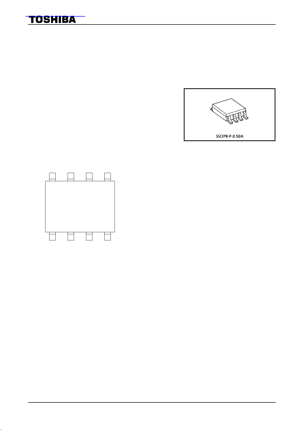
Pin Assignment
(top view)
Weight: 0.01 g (typ.)
TAR8H02K
V
OUT
CONTROL NOISE (A) NOISE (B) GND
V
(A)
8 7 6 5
1 2 3
(A) V
IN
IN
(B) V
OUT
(B)
V
(A) = 2.8 V
OUT
V
(B) = 2.8 V
OUT
4
Marking
8H02
Overtemperature protection and overcurrent protection functions are not necessary guarantee of operating
ratings below the absolute maximum ratings.
Do not use devices under conditions in which their absolute maximum ratings will be exceeded.
1
2007-11-01
TAR8H02K
<
f<
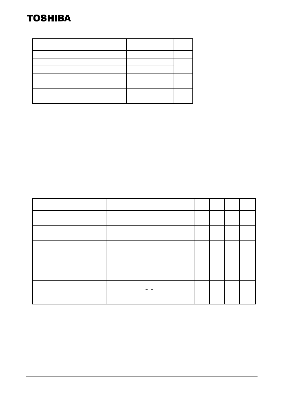
Absolute Maximum Ratings
Characteristics Symbol Rating Unit
Supply Voltage VIN 12 V
Output Current (A-channel) I
Output Current (B-channel) I
Power Dissipation PD
Operation Temp. Range T
Storage Temp. Range T
(Ta = 25°C)
(A) 100
OUT
(B) 150
OUT
opr
stg
mA
200 (Note 1)
400 (Note 2)
−40 to 85 °C
−55 to 150 °C
mW
Note: Using continuously under heavy loads (e.g. the application of high temperature/current/voltage and the
significant change in temperature, etc.) may cause this product to decrease in the reliability significantly even
if the operating conditions (i.e. operating temperature/current/voltage, etc.) are within the absolute maximum
ratings and the operating ranges.
Please design the appropriate reliability upon reviewing the Toshiba Semiconductor Reliability Handbook
(“Handling Precautions”/“Derating Concept and Methods”) and individual reliability data (i.e. reliability test
report and estimated failure rate, etc).
Note 1: Unit Rating
Note 2: Mounted on a glass epoxy circuit board of 30 × 30 mm Pad dimension of 70 mm
2
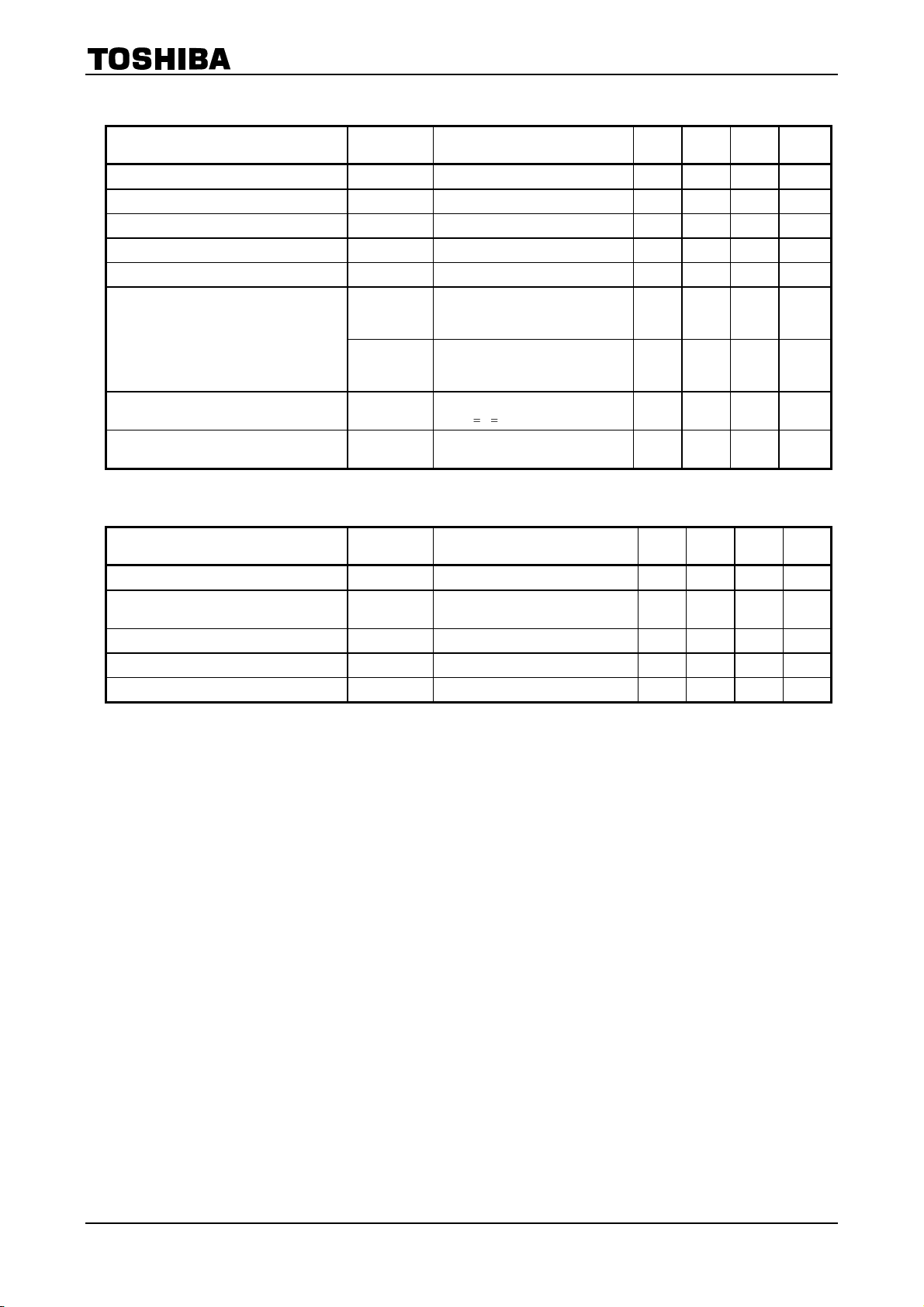
Electrical Characteristics
C
= 0.01 μF, VCT = 3.6 V, Tj = 25°C)
NOISE
(unless otherwise specified, VIN = 3.6 V, CIN = 1 μF, C
OUT
= 10 μF,
2.8 V Output Characteristics
Characteristics Symbol Test Condition Min Typ. Max Unit
Output Voltage V
Dropout Voltage VIN-V
Load Regulation Reg・load (A) I
Line Regulation Reg・line (A) VIN = 4.0 V to 8.0 V ⎯ 1 20 mV
Temp. Coefficient T
Ripple Rejection
Output Noise Voltage VNO (A)
Output Rise Time t
(
V
OUT
)
(A)
(A) I
OUT
(A) VIN = 2.6 V, I
OUT
(A) Ta = −40°C to 85°C ⎯ 100 ⎯ ppm/°C
CVO
R.R.1 (A)
(A)
R.R.
2
(A)
rise
(A) = 30 mA 2.72 2.8 2.88 V
OUT
(A) = 30 mA ⎯ 130 200 mV
OUT
(A) = 0 mA to 30 mA ⎯ 10 30 mV
OUT
V
= 5.0 V, I
IN
f = 200 Hz, V
Ta = 25°C
V
= 5.0 V, I
IN
f = 200 kHz, V
Ta = 25°C
I
(A) = 10 mA,
OUT
10 Hz
I
(A) = 30 mA,
OUT
= 0 V→3 V (tr = 10 ns)
V
CT
(A) = 10 mA,
OUT
= 1 V
Ripple
(A) = 10 mA,
OUT
Ripple
10 kHz, Ta = 25°C
= 1 V
p-p
,
p-p
,
⎯ 65 ⎯ dB
⎯ 50 ⎯ dB
⎯ 30 ⎯ μV
⎯ 1 ⎯ ms
rms
2
2007-11-01
TAR8H02K
<
f<
2.8 V Output Characteristics
Characteristics Symbol Test Condition Min Typ. Max Unit
Output Voltage V
Dropout Voltage VIN-V
Load Regulation Reg・load (B) I
Line Regulation Reg・line (B) VIN = 4.0 V to 8.0 V ⎯ 1 20 mV
Temp. Coefficient T
Ripple Rejection
Output Noise Voltage VNO (B)
Output Rise Time t
(
V
OUT
)
(B)
(B) I
OUT
(B) VIN = 2.6 V, I
OUT
(B) Ta = −40℃ to 85℃ ⎯ 100 ⎯ ppm/°C
CVO
R.R.1 (B)
R.R.
(B)
2
(B)
rise
(B) = 30 mA 2.72 2.8 2.88 V
OUT
(B) = 30 mA ⎯ 120 190 mV
OUT
(B) = 0 mA to 30 mA ⎯ 10 30 mV
OUT
V
= 5.0 V, I
IN
f = 200 Hz, V
Ta = 25°C
V
= 5.0 V, I
IN
f = 200 kHz, V
Ta = 25°C
I
(B) = 10 mA,
OUT
10 Hz
I
(B) = 30 mA,
OUT
= 0 V→3 V (tr = 10 ns)
V
CT
(B) = 10 mA,
OUT
= 1 V
Ripple
(B) = 10 mA,
OUT
Ripple
10 kHz, Ta = 25°C
= 1 V
p-p
,
p-p
,
⎯ 65 ⎯ dB
⎯ 50 ⎯ dB
⎯ 30 ⎯ μV
⎯ 1 ⎯ ms
Common Characteristics
Characteristics Symbol Test Condition Min Typ. Max Unit
rms
Stand-by Current I
Quiescent Current IB
Control Voltage (ON) V
Control Voltage (OFF) V
Control Input Current ICT VCT = 3 V (output ON) ⎯ ⎯ 30 μA
VCT = 0 V ⎯ ⎯ 10 μA
B (OFF)
I
(A) = 30 mA,
OUT
(B) = 30 mA
I
OUT
⎯ 2.2 ⎯ VIN V
CT (ON)
⎯ ⎯ ⎯ 0.4 V
CT (OFF)
⎯ 0.8 1.8 mA
3
2007-11-01

Application Note・ Recommended Application circuit
V
(A)
OUT
10 μF
8 7 6 5
1 2 3
CONTROL NOISE (A) NOISE (B) GND
The noise capacitor should be connected to NOISE pin
to GND for stable operation.
The recommended value is higher than 0.0047μF.
(A) V
V
IN
1 μF
0.01 μF
(B) V
IN
1 μF
0.01 μF
OUT
(B)
10 μF
Control level A-channel B-channel
4
The figure above shows commended configuration for using a point regulator. Insert a capacitor for stable
input/output operation.
If the control function is not to be used, Toshiba recommended that the control pin be connected to the
V
pin.
CC
・
TAR8H02K
HIGH ON ON
LOW OFF OFF
4
2007-11-01

TAR8H02K
Ripple Rejection
TAR8H02K feature a circuit with an excellent ripple rejection characteristic. Because the circuit also
features an excellent output fluctuation characteristic for sudden supply voltage drops, the circuit is ideal for
in the RF blocks incorporated in all mobile telephones.
80
Ripple Rejection − f
Input Transient Responce
70
60
50
40
30
20
Ripple Rejection (dB)
10
0
10 100 1 k 10 k 100 k 300 k
VIN = 3.6 V, C
CIN = 1 μF, V
I
out
NOISE
ripple
= 10 mA, Ta = 25°C
Frequency f (Hz)
= 0.01 μF,
= 1V
p−p
10 μF
2.2 μF
1 μF
,
3.4 V
3.1 V
2.8 V
01 45 8 10
2 3 6 7 9
NOISE Pin
TAR8H02K device incorporate a NOISE pin to reduce output noise voltage. Inserting a capacitor between
the NOISE pin and GND reduces output noise. To ensure stable operation, insert a capacitor of 0.0047 μF or
more between the NOISE pin and GND.
60
(μV)
N
50
40
30
20
10
Output noise voltage V
0
0.001 μ 0.01 μ 1.0 μ0.1 μ
NOISE capacitance C
C
NOISE
− VN
CIN = 1 μF, C
I
= 10 mA, Ta = 25°C
out
NOISE
= 10 μF,
out
(F)
Ta = 25°C, CIN = 1 μF,
C
= 10 μF, C
out
VIN: 3.4 V → 3.1 V, I
time t (ms)
Input Voltage
Output voltage
= 0.01 μF,
NOISE
= 30 mA
out
5
2007-11-01

TAR8H02K
(V)
OUT
6
5
4
3
I
OUT
C
NOISE
V
– VIN
OUT
= 1 mA, CIN = 1 μF, C
= 0.01 μF Pulse width = 1 ms
OUT
= 10 μF,
10
)
Hz
(μV/
N
1
VIN = 3.6 V, I
C
= 10 μF, C
OUT
10 Hz < f < 100 kHz, Ta = 25°C
0.1
V
– f
N
= 10 mA, CIN = 1 μF,
OUT
= 0.01 μF,
NOISE
2
Output voltage V
1
0
0 5 10 15
Input voltage VIN (V)
0.01
Output noise voltage V
0.001
10 100 1 k 10 k 100 k
Frequency f (Hz)
500
P
– Ta
D
400
(mW)
D
300
200
Circuit board material: grass epoxy.
Power dissipation P
Circuit board dimension: 30 mm × 30 mm
2
Pad area: 70 mm
100
−40
(t = 0.8mm)
0 40 120 80
Ambient temperature Ta (°C)
6
2007-11-01

Package Dimensions
TAR8H02K
Weight: 0.01 g (Typ.)
7
2007-11-01

TAR8H02K
RESTRICTIONS ON PRODUCT USE
• The information contained herein is subject to change without notice.
• TOSHIBA is continually working to improve the quality and reliability of its products. Nevertheless, semiconductor
devices in general can malfunction or fail due to their inherent electrical sensitivity and vulnerability to physical
stress. It is the responsibility of the buyer, when utilizing TOSHIBA products, to comply with the standards of
safety in making a safe design for the entire system, and to avoid situations in which a malfunction or failure of
such TOSHIBA products could cause loss of human life, bodily injury or damage to property.
In developing your designs, please ensure that TOSHIBA products are used within specified operating ranges as
set forth in the most recent TOSHIBA products specifications. Also, please keep in mind the precautions and
conditions set forth in the “Handling Guide for Semiconductor Devices,” or “TOSHIBA Semiconductor Reliability
Handbook” etc.
• The TOSHIBA products listed in this document are intended for usage in general electronics applications
(computer, personal equipment, office equipment, measuring equipment, industrial robotics, domestic appliances,
etc.).These TOSHIBA products are neither intended nor warranted for usage in equipment that requires
extraordinarily high quality and/or reliability or a malfunction or failure of which may cause loss of human life or
bodily injury (“Unintended Usage”). Unintended Usage include atomic energy control instruments, airplane or
spaceship instruments, transportation instruments, traffic signal instruments, combustion control instruments,
medical instruments, all types of safety devices, etc.. Unintended Usage of TOSHIBA products listed in his
document shall be made at the customer’s own risk.
• The products described in this document shall not be used or embedded to any downstream products of which
manufacture, use and/or sale are prohibited under any applicable laws and regulations.
• The information contained herein is presented only as a guide for the applications of our products. No
responsibility is assumed by TOSHIBA for any infringements of patents or other rights of the third parties which
may result from its use. No license is granted by implication or otherwise under any patents or other rights of
TOSHIBA or the third parties.
20070701-EN GENERAL
• Please contact your sales representative for product-by-product details in this document regarding RoHS
compatibility. Please use these products in this document in compliance with all applicable laws and regulations
that regulate the inclusion or use of controlled substances. Toshiba assumes no liability for damage or losses
occurring as a result of noncompliance with applicable laws and regulations.
8
2007-11-01
 Loading...