Toshiba TA8493BF Datasheet

Toshiba Bipolar Linear Integrated Circuit Multi-Chip
TA8493F, TA8493AF, TA8493BF
3-Phase Full Wave Brushless DC Motor Driver IC for CD-ROM Drives
These 3-phase, full-wave, brushless DC motor driver ICs have
been developed for use in CD-ROM drive spindle motors. The
TA8493F/ AF/ BF contain in its upper stage a discrete power
transistor (P-ch-MOS) and uses direct PWM control system,
which enables the IC to provide superior thermal efficiency.
Furthermore, the multi-chip structure of this device facilitates
dispersion of the heat generated inside the package, making it
possible to suppress heat concentration.
Features
· Multi-chip structure (3 × 2SJ465 chips built-in)
· Direct PWM control system
· Drive system: 120°drive system (TA8493F/BF)
: 180°drive system (TA8493AF)
· Built-in current limiter: I
· Built-in reversing brake/short brake functions
· FG signal output (using hall element output signal)
· Built-in hall bias
· Built-in thermal shutdown circuit
· Package: MFP-30
= 0.7 A (typ.) (at RF = 0.33 Ω)
LIM
Weight: 0.63 g (typ.)
TA8493F/AF/BF
1
2002-01-31
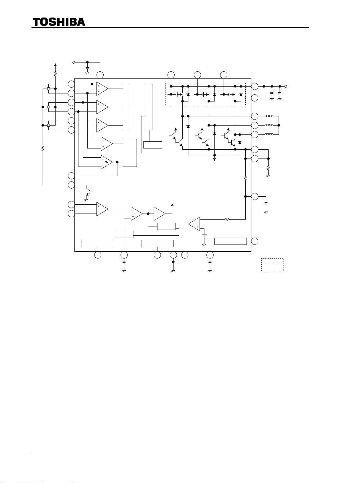
Block Diagram
f
V
CC
5 V
15
+
H
a
14
-
H
a
13
+
H
b
12
-
H
b
16
+
H
c
17
-
H
c
10
FGO
18
HB
21
V
C
V
22
re
L
La (G)
V
CC
Matrix
Amplifier
20 2 1 27
(G) Lc (G)
b
TSD
Reverse
Detection
GND
PWM Signal
TA8493F/AF/BF
V
29
4
3
30
28
6
25
8
M1
V
M2
L
a
L
b
L
c
R
F1
R
F2
C
RF
12 V
F/F
OSC
SB
Mode Select
MS
OSC
Short Brake
23 1924 71126
BRK
GND1
GND2
Stand by
C
d
5
2SJ465 ´ 3
9 pin: N.C.
2
2002-01-31

PIN Assignment
TA8493F/AF/BF
Terminal
No.
1 Lb (G)
2 La (G)
3 La a-phase output terminal Connect to the coil.
4 VM2 Supply voltage terminal for motor drive Connect to VM1 externally.
5 SB RUN/STOP control terminal H: RUN, L: STOP
6 RF1 Output current detection terminal
7 GND2 GND ¾
8 CRF Output current filter terminal
9 N.C.
10 FGO FG amplifier output terminal
11 BRK Brake mode select terminal Output mode when VC > V
12 H
13 H
14 H
15 H
16 H
17 H
18 HB Hall element bias terminal
19 Cd
20 VCC Supply voltage terminal for control circuits V
21 VC Control amplifier input terminal Use the control signal as input.
22 V
23 OSC Triangular wave oscillation terminal
24 GND1 GND ¾
25 RF2 Output current detection terminal
26 MS Mode select terminal Determines output mode.
27 Lc (G)
28 Lc c-phase output terminal Connect to the coil.
29 VM1 Supply voltage terminal for motor drive Connect to VM2 externally.
30 Lb b-phase output terminal Connect to the coil.
Terminal
Symbol
b-phase upper side power transistor (base)
output terminal
a-phase upper side power transistor (base)
output terminal
-
b-phase negative hall signal input terminal Connect to hall element output terminal.
b
+
b-phase positive hall signal input terminal Connect to hall element output terminal.
b
-
a-phase negative hall signal input terminal Connect to hall element output terminal.
a
+
a-phase positive hall signal input terminal Connect to hall element output terminal.
a
+
c-phase positive hall signal input terminal Connect to hall element output terminal.
c
-
a-phase negative hall signal input terminal Connect to hall element output terminal.
c
Forward/reverse changeover gain
adjustment terminal
ref
Control amplifier reference voltage input
terminal
c-phase upper side power transistor (base)
output terminal
Function Remarks
Keep open.
Keep open.
Sets limiter current value.
Connect to R
terminal and GND.
Connect a capacitor between this terminal
and GND.
Outputs a signal whose frequency is
determined by the CD rotation frequency.
Open collector output. Connect to the
negative side of hall element bias line.
Adjust a rotation direction changeover gain
CC (opr)
Use the reference voltage for the control
amplifier as input.
Connect a capacitor between this terminal
and GND.
Sets limiter current value.
Connect to R
terminal and GND.
Keep open.
externally and between this
F2
= 4.5 to 5.5 V
externally and between this
F1
ref
3
2002-01-31
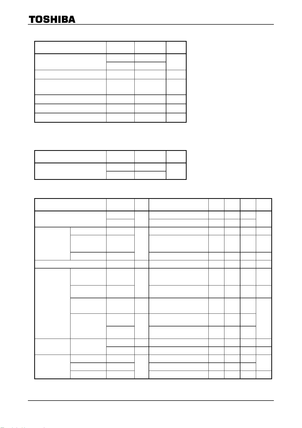
TA8493F/AF/BF
Absolute Maximum Ratings
Characteristics Symbol Rating Unit
Power Supply Voltage
Output Current IO 1.5 A
Power Dissipation
Junction Temperature Tj 150 °C
Operating Temperature T
Storage Temperature T
(Ta ==== 25°C)
VCC 7
V
16
M
P
D
(Note1)
opr
stg
V
1.0 W
-20 to 75 °C
-55 to 150 °C
Note1: unmounted
Operating Voltage Range
Characteristics Symbol
Power Supply Voltage
Electrical Characteristics
VCC 4.5 to 5.5
V
10 to 14
M
(VCC ==== 5 V, VM ==== 12 V, Ta ==== 25°C)
Operating
Range
Unit
V
Characteristics Symbol
I
V
V
DV
DV
INS (L)
CC1
I
CC2
INH
CMRH
H
CMRC
INC
V
DZ
OFF (F)
OFF (R)
I
LIM
V
LIM
INS (H)
INS (L)
Supply Voltage
Input Current I
Hall Amp.
Hall Element Bias Saturation Voltage VHB 2 IHB = 10 mA ¾ 1.3 2.0 V
Control Amp.
Current Limit
Amp.
RUN/STOP
Control Circuit
Common Mode
Input Voltage
Range
Input Amplitude V
Common Mode
Input Voltage
Range
Input Current I
Dead Zone
Voltage Width
Input Offset
Voltage
Limit Current
Input Voltage (H) V
Input Voltage (L) V
Input Current I
Test
Circuit
Stop mode ¾ 0.3 0.8
V
¾
¾ RF = 0.33 W (Note2) ¾ 700 ¾ mA
3 ¾ 0.25 0.3 0.35 V
1
Run mode, output open ¾ 7 15
2
¾ 1.5 ¾ 4.0 V
¾ 0.5 ¾ 4.0 V
2
V
(source current)
V
(RUN) 3.0 ¾ V
(STOP) GND ¾ 1.0
CW mode, V
R
2
CCW mode, V
R
1
V
Test Condition Min Typ. Max Unit
= 2.5 V, (sink current) ¾ ¾ 2 mA
CMRH
¾ 100 ¾ ¾ mV
= V
= 1.65 V,
C
ref
= 1.65 V, RF = 0.33 W
ref
(Note2)
= 1.65 V,
= 0.33 W
F
= 0.33 W
F
INS
ref
= 1.65 V,
ref
= GND, (source current) ¾ ¾ 1 mA
¾ ¾ 5.0 mA
¾ 100 ¾
20 50 150
20 50 150
CC
mA
p-p
mV
V
Note2: this is not tested.
4
2002-01-31
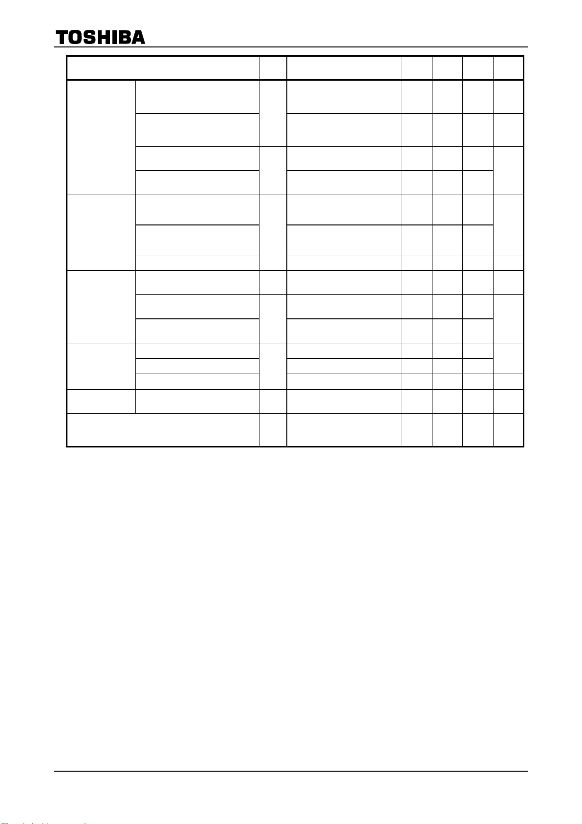
TA8493F/AF/BF
Characteristics Symbol
Output
Resistance
(upper side)
Saturation
Output Circuit
Voltage
(lower side)
Cut-off Current
(upper side)
Cut-off Current
(lower side)
Input Voltage (H) V
Mode Select
Circuit
Input Voltage (L) V
Input Current I
Hysteresis
Voltage
FG Amp.
Output Voltage
(H)
Output Voltage
(L)
Input Voltage (H) V
Short Brake
Circuit
Input Voltage (L) V
Input Current I
Triangular
Oscillation Circuit
Oscillation
Frequency
Thermal Shut-down Operating
Temperature
Test
Circuit
R
I
ON (U)
Test Condition Min Typ. Max Unit
= 0.6 A ¾ 0.5 1.0 W
O
4
V
SAT (L)
I
V
L (U)
IO = 0.6 A ¾ 0.4 0.8 V
= 16 V ¾ ¾ 10
L
5
I
L (L)
MS (H)
MS (L)
INMS
V
8 ¾ 5 20 45 mV
HYS
V
V
Source current: 10 mA
OFG (H)
OFG (L)
¾ 3.0 ¾ V
BRK (H)
¾ ¾ ¾ 0.5
BRK (L)
INBRK
f
¾ C = 560 pF (Note2) ¾ 39 ¾ kHz
OSC
VL = 16 V ¾ ¾ 10
CCW mode
> V
C
C
> V
, BRK: L
ref
, BRK: L
ref
V
6
Reversing brake mode
V
3.0 ¾ V
¾ ¾ 0.5
VMS = GND, (source current) ¾ ¾ 1 mA
V
CC
7
- 0.5
¾ ¾
Sink current: 10 mA ¾ ¾ 0.5
6
V
= GND, (source current) ¾ ¾ 1 mA
BRK
Junction temperature
TSD ¾
(according to design
¾ 175 ¾ °C
specification) (Note2)
CC
CC
mA
V
p-p
V
V
Note2: this is not tested.
5
2002-01-31
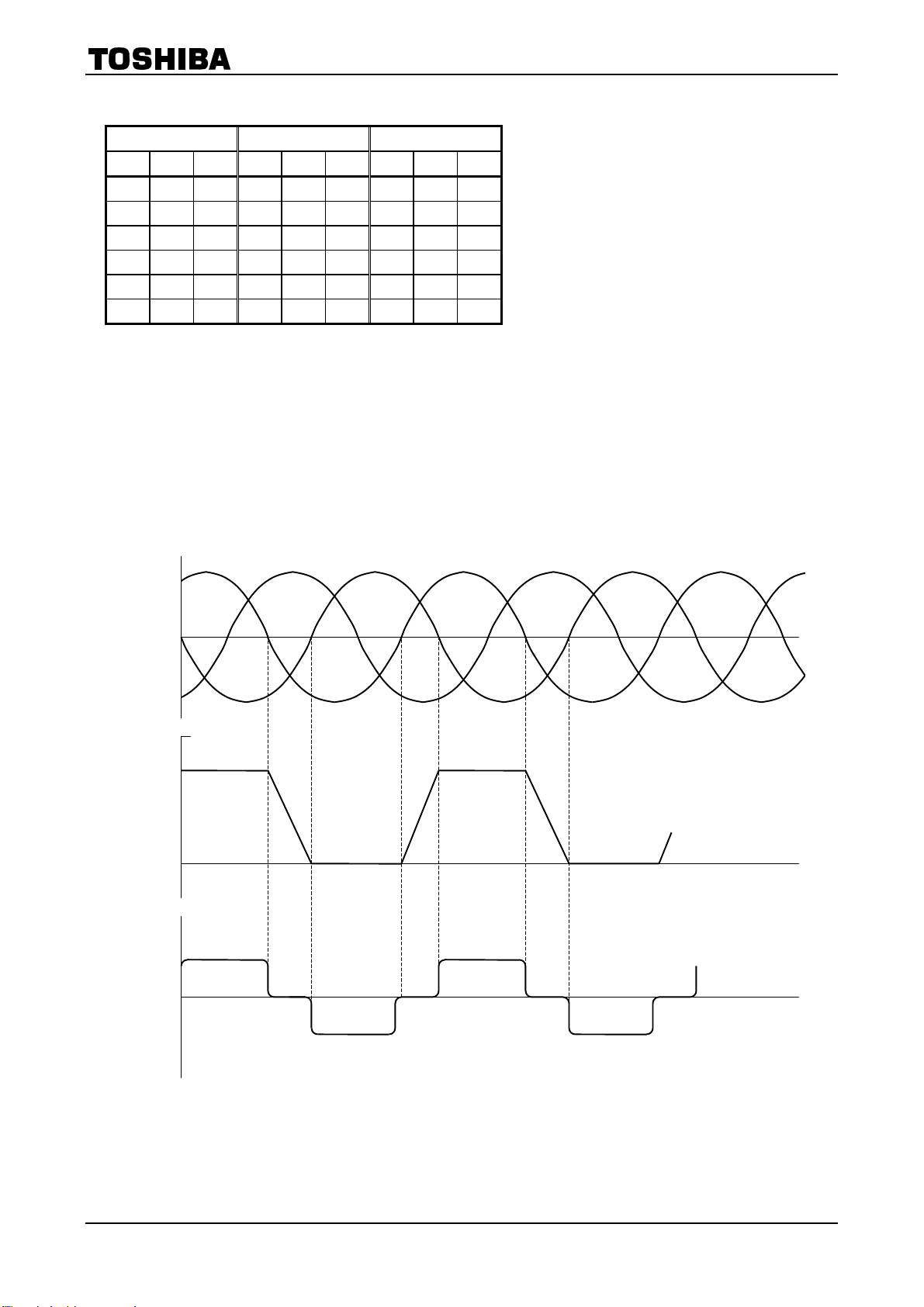
Function Table
Forward Reverse
Ha Hb Hc La Lb Lc La Lb Lc
H L L H L M L H M
H H L H M L L M H
L H L M H L M L H
L H H L H M H L M
L L H L M H H M L
H L H M L H M H L
<Forward> <Reverse>
La = -(Hc - Ha) La = (Hc - Ha)
L
= -(Ha - Hb) Lb = (Ha - Hb)
b
L
= -(Hb - Hc) Lc = (Hb - Hc)
c
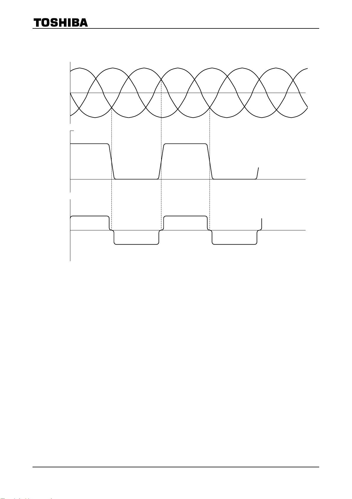
Timing Diagram
<Forward>
(TA8493F/BF)
H
a
+
H
b
H
c
TA8493F/AF/BF
Hall Signal
V
Output Voltage
GND
Output Current
-
L
M
+
-
a
6
2002-01-31
(TA8493AF)
Hall Signal
Output Voltage
GND
TA8493F/AF/BF
H
a
+
-
V
M
H
b
H
c
L
a
Output Current
+
-
7
2002-01-31
Functional Description
This IC is a 3-phase, full wave brushless DC motor driver of the direct PWM control type.
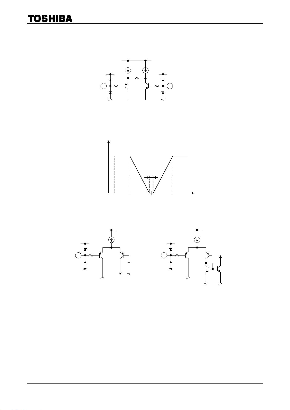
· Control amp input circuit
V
CC
TA8493F/AF/BF
V
C
V
ref
The common mode input voltage ranges for both V
and V
C
are 0.5 to 4.0 V.
ref
Relation between control input and PWM ON duty is shown below, PWM ON duty is 100%
when ïV
- VCï = 0.75 V (typ.)
ref
The input is provided with a dead-zone area whose voltage width is 100 mV (typ.)
100
Dead-zone
voltage width
100 mV (typ.)
PWM on duty (%)
0.5
V
- 0.75 V
ref
V
ref
VC (V)
ref
+ 0.75
· Mode select/short brake circuit
MS
BRK
8
2002-01-31
 Loading...