

TOSHIBA Bipola r Linear Integrated Circuit Silicon Monolithic
TA8266HQ
Max Power 35 W BTL × 4 ch Audio Power IC
The TA8266HQ is 4 ch BTL audio power amplifier for car audio
application.
This IC can generate more high power: P
is included the pure complementary PNP and NPN transistor
output stage.
It is designed low distortion ratio for 4 ch BTL audio power
amplifier, built-in stand-by function, muting function, and
diagnosis circuit which can detect output to V
over voltage input mode.
Additionally, the AUX amplifier and various kind of protector
for car audio use is built-in.
Features
MAX = 35 W as it
OUT
/GND short and
CC
Weight: 7.7 g (typ.)
TA8266HQ
• High power : P
(V
: P
(V
: P
(V
: P
(V
• Built-in diagnosis circuit (pin 25)
• Low distortion ratio: THD = 0.02% (typ.)
(V
• Low noise: V
(V
• Built-in stand-by switch function (pin 4)
• Built-in muting function (pin 22)
• Built-in AUX amplifier from single input to 2 channels output (pin 16)
• Built-in various protection circuit
: Thermal shut down, over voltage, out to GND, out to V
• Operating supply voltage: V
Note 1: Install the product correctly. Otherwise, it may result in break down, damage and/or degradation to the
product or equipment.
Note 2: These protection functions are int ended to avoid some ou tput short circuits or other abnormal conditions
temporarily. These protect functi ons do not warrant to prevent the IC from being damaged.
- In case of the product would be operated with exceeded guaranteed operating ranges, these
protection features may not operate and some output short circuits may result in the IC being
damaged.
MAX (1) = 35 W (typ.)
OUT
= 14.4 V, f = 1 kHz, JEITA max, RL = 4 Ω)
CC
MAX (2) = 31 W (typ.)
OUT
= 13.7 V, f = 1 kHz, JEITA max, RL = 4 Ω)
CC
(1) = 23 W (typ.)
OUT
= 14.4 V, f = 1 kHz, THD = 10%, RL = 4 Ω)
CC
(2) = 20 W (typ.)
OUT
= 13.2 V, f = 1 kHz, THD = 10%, RL = 4 Ω)
CC
= 13.2 V, f = 1 kHz, P
CC
= 0.18 mVrms (typ.)
NO
= 13.2 V, Rg = 0 Ω, GV = 34dB, BW = 20 Hz~20 kHz)
CC
= 9~18 V
CC (opr)
= 5 W, RL = 4 Ω)
OUT
CC
, out to out short, speaker burned
1
2006-04-28
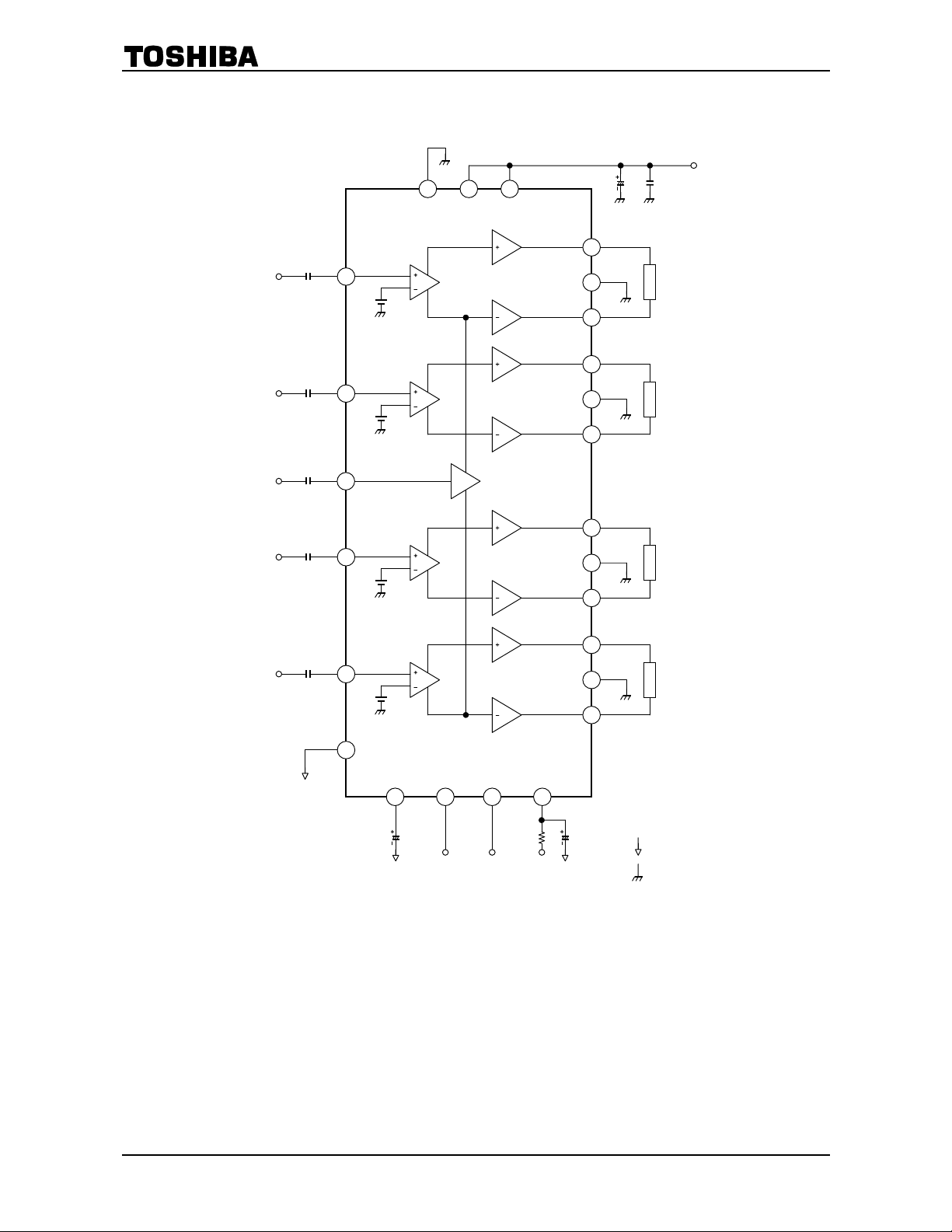
Block Diagram
TA8266HQ
C1
C1
C6
C1
11
12
16
15
IN1
IN2
AUX IN
IN3
1 20 6
TAB V
CC1VCC2
OUT1 (+)
PW-GND1
OUT1 (−)
OUT2 (+)
PW-GND2
OUT2 (−)
OUT3 (+)
PW-GND3
OUT3 (−)
17
18
19
5
C
9
8
7
5
2
3
3
C
RL
RL
RL
C1
PRE-GND
14
13
IN4
DIAGNOSIS
STBY
10 254 22
2
C
OUT RIP MUTE
OUT4 (+)
PW-GND4
OUT4 (−)
1
R
21
24
23
4
C
RL
: PRE-GND
: PW-GND
Note3: Some of the functional bl ocks, circuits, or constants in the block diagram may be omitted or si mplified for
explanatory purpose.
2
2006-04-28
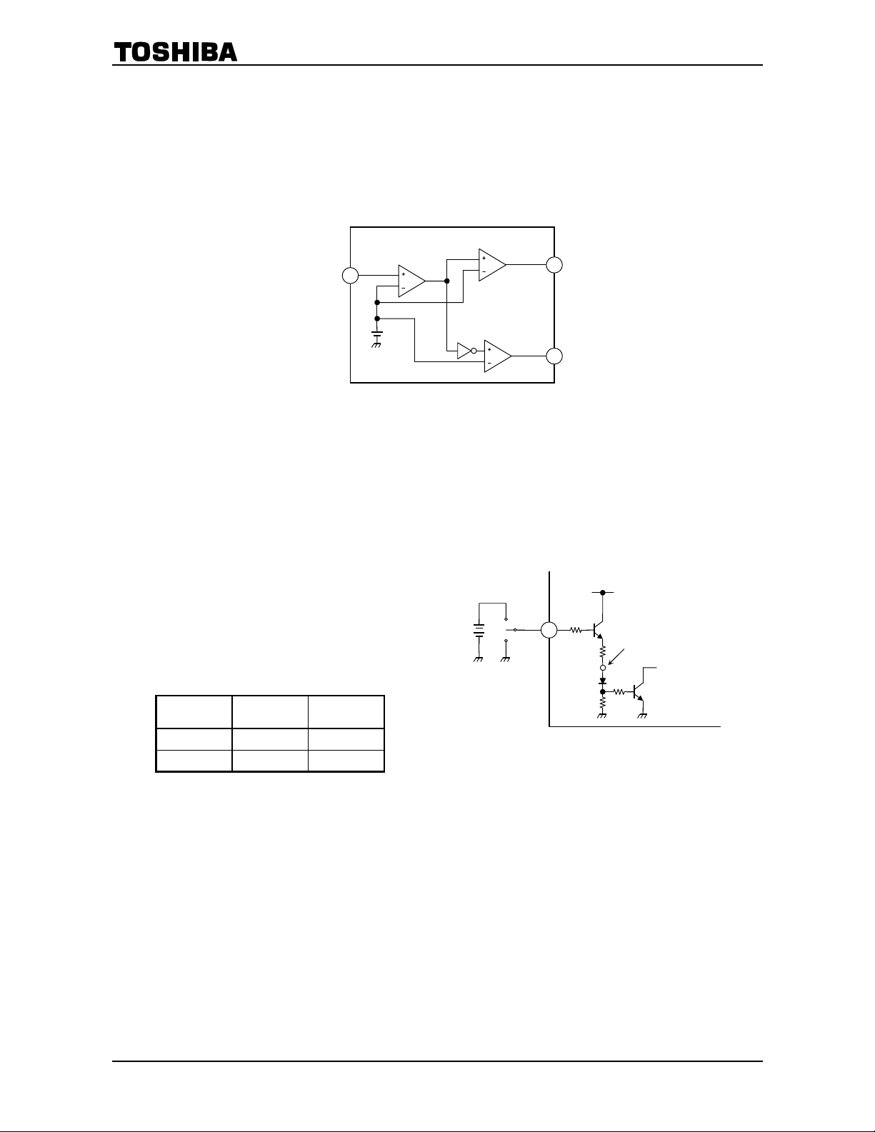
Caution and Application Method
(Description is made only on the single channel.)
1. Voltage Gain Adjustment
This IC has no NF (negative feedback) terminals. Therefore, the voltage gain can’t adjusted, but it makes
the device a space and total costs saver.
Amp. 1
Input
Figure 1 Block Diagram
The voltage gain of Amp.1 : G
The voltage gain of Amp.2A, B : G
The voltage gain of BLT Connection : G
Therefore, the total voltage gain is decided by expression below.
G
= GV1 + GV2 + G
V
2. Stand-by SW Function
By means of controlling pin 4 (stand-by terminal) to
high and low, the power supply can be set to ON and
OFF. The threshold voltage of pin 4 is set at about
3V
(typ.), and the power supply current is about 2
BE
µA (typ.) at the stand-by state.
Control Voltage of pin 4: VSB
= 8 + 20 + 6 = 34dB
V (BTL)
(pin 4)
V1
V2
V (BTL)
Amp. 2A
= 8dB
= 20dB
= 6dB
Amp. 2B
ON
OFF
Power
4
10 kΩ
V
CC
≈ 2VBE
TA8266HQ
to BIAS
CUTTING CIRCUIT
Stand-by Power VSB (V)
ON OFF 0~1.5
OFF ON 3~VCC
Figure 2 With pin 4 set to High,
Power is turned ON
Adjustage of Stand-by SW
(1) Since V
omitted.
(2) Since the control current is microscopic, the switching relay of small current capacity is satisfactory
for switching
can directly be controlled to ON or OFF by the microcomputer, the switching relay can be
CC
3
2006-04-28
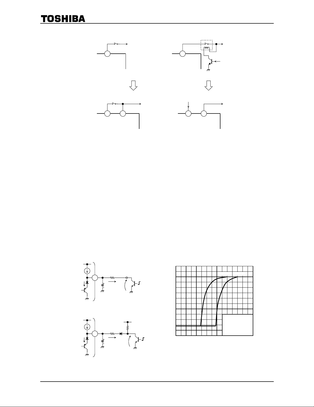
TA8266HQ
A
Large current capacity switch
BATTERY
RELAY
BATTERY
Stand-By V
3. Muting Function (pin 22)
By means of controlling pin 22 less than 0.5 V, it can make the audio muting condition.
The muting time constant is decided by R
ON/OFF.
The series resistance; R1 must be set up less than 10 kΩ to get enough muting attenuation.
The muting function have to be controlled by a transistor, FET and micro-controller port which has
I
> 250 µA ability.
MUTE
Pin 22 terminal voltage has the temperature characteristics of 4.6 V (low temperature) to 3.2 V (high
temperature).
Therefore, it is need to design with attention as using the micro-controller of which operating voltage is
less than 5 V.
Terminal 22 may not be pulled up and shall be controlled by OPEN/LOW.
When it is obliged to do, it must be pulled up via diode, because it has to defend flowing reverse current
to internal circuit of pin 22.
<Recommended Application>
I (100 µA)
I
MUTE (OFF)
22
4
C
V
CC
Small current capacity switch
R1
MUTE
V
V
MUTE
CC
I
V
CC
– Conventional Method –
DIRECTLY FROM
BATTERY
– Stand-by Switch Method –
MICROCOMPUTER
Stand-By
CC
FROM
MICROCOMPUTER
BATTERY
Figure 3
and C4 and these parts is related the pop noise at power
1
20
0
−20
−40
ATT – V
MUTE
10 kΩ 5 kΩ
<Application for pulled up>
I (100 µA)
I
MUTE (OFF)
22
R1
4
C
I
MUTE
V
MUTE
Figure 4 Muting Function
−60
MUTE
VCC = 13.2 V
Po = 10 W
PL = 4 Ω
f = 1 kHz
(V)
−80
Mute attenuation ATT (dB)
−100
0 0.4 0.8 1 1.2 1.6 2 2.4 2.8 3
Point A voltage: V
Figure 5 Mute Attenuation − V
4
(V)
MUTE
2006-04-28
TA8266HQ
4. AUX Input (pin 16)
The pin 16 is for input terminal of AUX
amplifier.
The total gain is 0dB by using of AUX amplifier.
Therefore, the µ-COM can directly drive the
AUX amplifier.
BEEP sound or voice synthesizer signal can be
input to pin 16 directly.
When AUX function is not used, this pin must be
connected to PRE-GND (pin 13) via a capacitor.
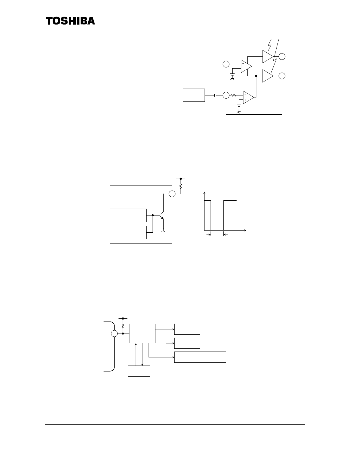
5. Diagnosis Output (pin 25)
This diagnosis output terminal of pin 25 has open collector output structure on chip as shown in Figure 7.
In case diagnosis circuit that detect unusual case is operated, NPN transistor (Q1) is turned on.
It is possible to protect all the system of apparatus as well as power IC protection.
In case of being unused this function, use this IC as open-connection on pin 25.
25
µ-COM
5 V
5 V
IN
AUX-IN
AUX AMP
16
−20dB
Figure 6 AUX Input
20dB AMP.
OUT (+)
OUT (−)
OUTPUT SHORT
PROTECTOR
OVER VOLTAGE
PROTECTOR
pin 25: O pen collector out put (active low)
Q1
GND
Figure 7 Self Diagnosis Output
5.1 In Case of Shorting Output to VCC/GND or Over Voltage Power Supplied
NPN transistor (Q1) is turned on.
Threshold of over voltage protection: V
5 V
25
µ-COM
MEMORY
(Count and record)
= 22 V (typ.)
CC
LED/LCD
ALARM
REGULATOR → OFF
(Flashing)
(Announcement from a speaker.)
Q1 is turned on
(Relay → OFF)
t
5.2 In Case of Shorting Output to Output
NPN transistor (Q1) is turned on and off in response to the input signal voltage.
Figure 8 Application 1
5
2006-04-28

6. Prevention of speaker burning accident (In Case of Rare Short Circuit of Speaker)
When the direct current resistance between OUT + and OUT − terminal becomes 1 Ω or less and output
current over 4 A flows, this IC makes a protection circuit operate and suppresses the current into a speaker.
This system makes the burning accident of the speaker prevent as below mechanism.
<The guess mechanism of a burning accident of the speaker>
Abnormal output offset voltage (voltage between OUT + and OUT −) over 4 V is made by the external
circuit failure.(Note 4)
↓
The speaker impedance becomes 1 Ω or less as it is in a rare short circuit condition.
↓
The current more than 4 A flows into the speaker and the speaker is burned.
Current into a speaker
Operating point of protector
Less than 4 Ω
TA8266HQ
About 1 Ω 4 Ω
Figure 9
Note 4: I t is appeared by biased input DC voltage
(for example, large leakage of the input capacitor , short-circuit between copper patterns of PCB.)
Speaker impedance
6
2006-04-28

6.1 Applications
When output terminals short-circuit to VCC or GND, the voltage of 25pin is fixed to “L”.
And when shorting OUT + to OUT −, “L” and “H” are switched according to an input signal.
Therefore, it is possible to judge how the power IC condition is if a micro-controller detects the
25pin voltage that is smoothed out with LPF.
It is recommend that the threshold voltage (Vth) is set up as higher as possible because output level
of LPF is changed according to an input signal.
(for example, Vth is set up to 4 V if 25pin is pulled up to 5 V line.)
TA8266HQ
Output voltage of L.P.F.
Operating point of protector
5 V
Output power
Figure 10
7
2006-04-28

TA8266HQ
Absolute Maximum Ratings
Characteristics Symbol Rating Unit
Peak supply voltage (0.2 s) V
DC supply voltage V
Operation supply voltage V
Output current (peak) I
Power dissipation PD (Note5) 125 W
Operation temperature T
Storage temperature T
Note5: Package thermal resistance θ
(Ta = 25°C)
CC (surge)
CC (DC)
CC (opr)
O (peak)
opr
stg
= 1°C/W (typ. )
j-T
50 V
25 V
18 V
−40~85 °C
9 A
−55~150 °C
(Ta = 25°C, with infinite heat sink)
The absolute maximum ratings of a semiconductor device are a set of specified parameter values, which must not
be exceeded during operation, even for an instant. If any of these rating would be exceeded during operation, the
device electrical characteristics may be irreparably altered and the reliability and lifetime of the device can no
longer be guaranteed. Moreover, these operations with exceeded ratings may cause break down, damage and/or
degradation to any other equipment. Applications using the device should be designed such that each absolute
maximum rating will never be exceeded in any operating conditions. Before using, creating and/or producing
designs, refer to and comply with the precautions and conditions set forth in this documents.
Electrical Characteristics
(unless otherwise specified VCC = 13.2 V, f = 1 kHz, RL = 4 Ω, Ta = 25°C)
Characteristics Symbol
Quiescent current I
Output power
Total harmonic distortion THD ⎯ P
Voltage gain GV ⎯ V
Voltage gain ratio ∆GV ⎯ V
Output noise voltage
Ripple rejection ratio R.R. ⎯
Cross talk C.T. ⎯
Output offset voltage V
Input resistance RIN ⎯ ⎯ ⎯ 30 ⎯ kΩ
Stand-by current ISB ⎯ Stand-by condition ⎯ 2 10 µA
Stand-by control voltage
Mute control voltage (Note6)
Mute attenuation ATT M ⎯
CCQ
P
MAX (1) ⎯ VCC = 14.4 V, max Power ⎯ 35 ⎯
OUT
P
MAX (2) ⎯ VCC = 13.7 V, max Power ⎯ 31 ⎯
OUT
P
OUT
P
OUT
VNO (1) ⎯ Rg = 0 Ω, DIN45405 ⎯ 0.20 ⎯
V
(2) ⎯ Rg = 0 Ω, BW = 20 Hz~20 kHz ⎯ 0.18 0.42
NO
OFFSET
VSB H ⎯ Power: ON 3.0 ⎯ VCC
V
SB
VM H ⎯ Mute: OFF Open ⎯
V
L ⎯ Mute: ON, R1 = 10 kΩ 0 ⎯ 0.5 V
M
Test
Circuit
⎯ VIN = 0 ⎯ 200 400 mA
(1) ⎯ VCC = 14.4 V, THD = 10% ⎯ 23 ⎯
(2) ⎯ THD = 10% 17 20 ⎯
⎯ ⎯ −150 0 +150 mV
L ⎯ Power: OFF 0 ⎯ 1.5
Test Condition Min Typ. Max Unit
= 5 W ⎯ 0.02 0.2 %
OUT
= 0.775 Vrms (0dBm) 32 34 36
OUT
= 0.775 Vrms (0dBm) −1.0 0 1.0
OUT
f
= 100 Hz, Rg = 620 Ω
rip
V
= 0.775 Vrms (0dBm)
rip
Rg = 620 Ω
V
= 0.775 Vrms (0dBm)
OUT
Mute: ON,
V
= 7.75 Vrms (20dBm) at
OUT
Mute: OFF.
W
dB
mVrms
40 50 ⎯ dB
⎯ 60 ⎯ dB
V
80 90 ⎯ dB
Note6: Muting function have to be contr ol l ed by open and low logic, whic h logic is a transistor, FET and µ-COM port
of I
> 250 µA ability.This means than the mute control terminal : pin 22 must not be pulled-up.
MUTE
8
2006-04-28

Te st Cir cuit
TA8266HQ
0.22 µF
C1
0.22 µF
C1
0.22 µF
C
6
0.22 µF
C1
11
12
16
15
IN1
IN2
AUX IN
IN3
1 20 6
TAB V
CC1VCC2
OUT1 (+)
PW-GND1
OUT1 (−)
OUT2 (+)
PW-GND2
OUT2 (−)
OUT3 (+)
PW-GND3
OUT3 (−)
17
18
19
5
C
9
8
7
5
2
3
3
C
0.1 µF
3900 µF
RL
RL
RL
0.22 µF
C1
PRE-GND
14
13
IN4
DIAGNOSIS
STBY
10 254 22
2
C
10 µF
OUT RIP MUTE
OUT4 (+)
PW-GND4
OUT4 (−)
1
R
10 kΩ
21
24
23
4
C
1 µF
RL
: PRE-GND
: PW-GND
9
2006-04-28
TA8266HQ
T.H.D – P
100
VCC = 13.2 V
RL = 4 Ω
OUT
T.H.D – P
100
f = 1 kHz
RL = 4 Ω
OUT
10
1
10 kHz
0.1
Total harmonic distortion T.H.D (%)
0.01
0.1
100 Hz
1 kHz
1
Output power P
OUT
10
(W)
100
I
400
RL = ∞
VIN = 0
300
(mA)
CCQ
200
100
Quiescent current I
0
Power supply voltage VCC (V)
– VCC
CCQ
10 0
20
30
10
1
16.0 V
10
(W)
13.2 V
100
0.1
Total harmon ic distortion T.H.D (%)
0.01
0.1
Output power P
9.0 V
1
OUT
T.H.D – f
1
0.1
OUT4
0.01
Total harmonic dist ortion T. H.D (%)
0.001
OUT3
OUT2, 3
10010
Frequency f (H z)
VCC = 13.2 V
RL = 4 Ω
P
= 5 W
out
1 k
10 k
100 k
10
2006-04-28

TA8266HQ
V
300
VCC = 13.2 V
RL = 4 Ω
250
BW = 20 Hz~20 kHz
(µVrms)
200
NO
150
100
50
Output noise voltage V
0
100 10
Singnal source resistance Rg (Ω)
NO
1 k
– Rg
10 k
100 k
R.R. – f
0
VCC = 13.2 V
RL = 4 Ω
−10
Rg = 620 Ω
−20
V
= 0dBm
rip
−30
−40
−50
Ripple rejection ratio R.R. (dB)
−60
−70
10010
1 k
10 k
100 k
Frequency f (H z)
C.T . – f (OUT1)
0
VCC = 13.2 V
RL = 4 Ω
−10
V
= 0dBm
OUT
−20
Rg = 620 Ω
−30
−40
−50
Cross talk C.T. (dB)
−60
−70
OUT1 → OUT2, 3, 4
100 10
1 k
10 k
100 k
Frequency f (H z)
C.T . – f (OUT3)
0
VCC = 13.2 V
RL = 4 Ω
−10
V
= 0dBm
OUT
−20
Rg = 620 Ω
C.T . – f (OUT2)
0
VCC = 13.2 V
RL = 4 Ω
−10
V
= 0dBm
OUT
−20
Rg = 620 Ω
−30
−40
−50
Cross talk C.T. (dB)
−60
−70
OUT2 → OUT1, 3, 4
10010
Frequency f (H z)
C.T . – f (OUT4)
0
VCC = 13.2 V
RL = 4 Ω
−10
V
= 0dBm
OUT
−20
Rg = 620 Ω
1 k
10 k
100 k
−30
−40
−50
Cross talk C.T. (dB)
−60
−70
100 10
OUT3 → OUT4
OUT3 → OUT1, 2
1 k
10 k
100 k
Frequency f (H z)
11
−30
−40
−50
Cross talk C.T. (dB)
−60
−70
10010
OUT4 → OUT1, 2, 3
1 k 10 k
100 k
Frequency f (H z)
2006-04-28

TA8266HQ
G
40
35
30
(dB)
25
V
20
15
10
Voltage gain G
5
0
100 10
Frequency f (H z)
1 k
V
– f
P
MAX –Ta
120
100
MAX (W)
D
80
①
60
D
① INFINITE HEAT SINK
RθJC = 1°C/ W
② HEAT SINK (RθHS = 3.5°C/W)
RθJC + RθHS = 4.5°C/W
③ NO HEAT SINK
RθJA = 39°C/W
VCC = 13.2 V
RL = 4 Ω
V
= 0dBm
OUT
10 k
100 k
P
70
60
50
(W)
D
Power dissipation P
40
30
20
10
0
9 V
5 15 20 10 25 0
Output power P
– P
D
13.2 V
OUT
OUT
16 V
f = 1 kHz
RL = 4 Ω
/ch (C)
40
20
Allowable power dissipation P
③
0
25 0
50 125
②
75
100
150
Ambient temperature Ta (°C)
12
2006-04-28

Package Dimensions
TA8266HQ
Weight: 7.7 g (typ.)
13
2006-04-28

TA8266HQ
14
2006-04-28

TA8266HQ
• Use an appr opriate power supply fuse to ensure that a large current does not continuously flow in case of over
current and/or IC failure. The IC will fully break down when used under conditions that exceed its absolute
maxim um r at i ng s , w he n t h e wi ring is r o ut e d i m p r o perly or wh en an abnormal pu l s e no i s e o c curs from the wi r i ng or
load, causing a large current to continuousl y flow and the breakdown can lead smoke or i gnition. To minimize the
effects of the flow of a large current in case of breakdown, appropriate settings, such as fuse capacity, fusing time
and insertion circuit location, ar e required.
• If your design includes a n inductive load such as a m otor coil, incorporate a pr otection circuit into the desi gn to
prevent device malfunction or breakdown ca used by the current resulting from t he inrush current at power ON or
the negative current resulting f rom the back electromotive force at power OFF. For details on how to connect a
protection circuit such as a current l imi ting resis tor or back electrom otive forc e adsorption di ode, refer to individ ual
IC datasheets or the IC databook. IC breakdown may cause injury, smoke or ignition.
• Use a stable power supply with ICs with built-in protection functions. If the power supply is unstable, the protection
function may not operate, causing IC breakdown. IC br eakdown may cause injury, smoke or ignition.
• Car efully select external components (such as inputs and negative feedback capacitors) and load comp onents
(such as speakers), for example, power amp and r egulator. If there is a l arge amount of leakage c urrent such as
input or negative feedback condenser, the IC output DC voltage will increase. If this output voltage is connected to
a speaker with low input withstand voltage, overcurrent or IC failure can cause smoke or ignition. (The over
current can cause smoke or ignition from the IC itself.) In particular, please pay attention when using a Bridge Tied
Load (BTL) connection type IC that inputs output DC voltage to a speaker directly.
• Over current Protection Circuit
Over current protection circuits (referred to as current limiter circuits) do not necessarily protect ICs under all
circumstances. If the Over current protection ci rcuits operate against the over c urrent, clear the over current status
immediately. Depending on the method of use and usage conditions, such as exceeding absolute maximum
ratings can cause the over current protectio n circuit to not operate pr operly or IC breakdown before operation. In
addition, depending on the metho d of use and usage conditions, if over current continues to flow f or a long time
after operation, the IC may generate heat resulting in br eakdown.
• Ther mal Shutdown Circuit
Thermal shutdown circuits do not necessarily protect ICs under all circumstances. If the Thermal shutdown circuits
operate against the over temperature, clear the heat ge neration status immediately. Depending on the method of
use and usage conditions, such as exceedi ng absolute maximum ratin gs can cause the thermal shutdown circ uit
to not operate properly or IC breakdown befor e oper ati on.
• Heat Radiation Design
When using an IC with large c urr ent flow s uch as power amp, r egulator or driver, please design the device so t hat
heat is appropriately radiated, not to exceed the specified junction temperature (Tj) at any time and condition.
These ICs generate heat even during normal use. An inadequate IC heat radiation design can lead to decrease in
IC life, deterioration of IC characteristics or IC breakdown. In addition, please design the device taking into
considerate the effect of IC heat radiation with peripheral components.
• Installation to Heat Sink
Please install the power IC to the heat sink not to apply excessive mechanical stress to the IC. Excessive
mechanical stress can lead to package cracks, resulting in a reduction in reliability or breakdown of internal IC
chip. In addition, depending on the IC, the use of silicon rubber may be prohibited. Check whether the use of
silicon rubber is prohi bited for the IC you intend to use, or not. For details of pow er IC heat ra diation design and
heat sink installation, refer to individual technical datas heets or IC databooks.
15
2006-04-28

TA8266HQ
RESTRICTIONS ON PRODUCT USE
060116EBF
• The information contained herein is subject to change without notice. 021023_D
• TOSHIBA is continually working to improve the quality and reliability of its products. Nevertheless, semiconductor
devices in general can malfunction or fail due to their inherent electrical sensitivity and vulnerability to physical
stress. It is the responsibility of the buyer, when utilizing TOSHIBA products, to comply with the standards of
safety in making a safe design for the entire syst em, and to avoid situations in which a malfunction or failure of
such TOSHIBA products could cause loss of human life, bodily injury or damage to property.
In developing your designs, please ensure t hat TOSHIBA products are used within specified operating ranges as
set forth in the most recent TOSHIBA products specifications. Also, please keep in mind the precautions and
conditions set forth in the “Handling Guide for Semiconductor Devices,” or “TOSHIBA Semiconductor Reliability
Handbook” etc.
021023_A
• The TOSHIBA products listed in this document are intended for usage in general electronics applications
(computer, personal equipment, office equipment, measur ing equipment , industrial robotics , domestic appli ances,
etc.). These TOSHIBA products are neither intended nor warranted for usage in equipment that requires
extraordinarily high quality and/or reliability or a malfunction or failure of which may cause loss of human life or
bodily injury (“Unintended Usage”). Unintended Usage include atomic energy control instruments, airplane or
spaceship instruments, transportation instruments, traffic signal instruments, combustion control instruments,
medical instruments, all types of safety devices, etc. Unintended Usage of TOSHIBA products listed in this
document shall be made at the customer’s own risk.
021023_B
• The products described in this document shall not be used or em bedded to any downstream pr oducts of which
manufacture, use and/or sale are prohibited under any appl icable laws and regulations.
060106_Q
• The information contained herein is presented only as a guide for the applications of our products. No
responsibility is assumed by TOSHIBA for any infringements of patents or other rights of the third parties which
may res ult from its use. N o license i s grante d by impli cation o r otherwi se under any patent or paten t rights of
TOSHIBA or others .
021023_C
• The products described in this document are subject to the for ei gn exchange and foreign trade laws.
021023_E
• This product g enerates heat dur ing normal o peration. However, substandard performance or malfunction may
cause the pr oduct and its p eriph erals to reach abnormally hig h temp eratures.
The product is often the final stage (the external output stage) of a circuit. Substandard performance or
malfunction of the destination devi ce to which the circuit supplies outp ut may cause damage to the cir cui t or to the
product.
030619_R
About solderability, following conditions were confirmed
• Solderability
(1) Use of Sn-37Pb solder Bath
· so lder bath temperature = 230°C
· dipping time = 5 seco nds
· the number of times = onc e
· use of R-type flux
(2) Use of Sn-3.0Ag-0.5Cu solder Bath
· so lder bath temperature = 245°C
· dipping time = 5 seco nds
· the number of times = onc e
· use of R-type flux
16
2006-04-28
 Loading...