

Page 1
TOSHIBA Bipolar Linear Integrated Circuit Silicon Monolithic
TA8246AHQ
Dual Audio Power Amplifier 6 W × 2 Ch
TA8246AHQ is dual power amplifier for Consumer applications.
This IC provides an output power of 6 watts per channel
(at V
It is suitable for power amplifier of TV and home Stereo.
Features
= 20 V, f = 1 kHz, THD = 10%, RL = 8 Ω).
CC
TA8246AHQ
• : High output power: P
(V
• Built-in audio muting circuit.
• NF terminal capacitor less
: Fixed gain (G
• Protectors
: Thermal shut down protection circuit, over voltage protection circuit
• Low poping noise
• High THD ratio
• High input dynamic range
• Available for using same PCB layout with 3 channel IC: TA8256BHQ
• Operating supply voltage range
: V
= 20 V, RL = 8 Ω, f = 1 kHz, THD = 10%)
CC
= 34dB), needless external capacitor.
v
CC (opr)
= 10~30 V (Ta = 25°C)
= 6 W (Typ.)
out
Weight: 4.04 g (typ.)
1
2004-07-12
Page 2
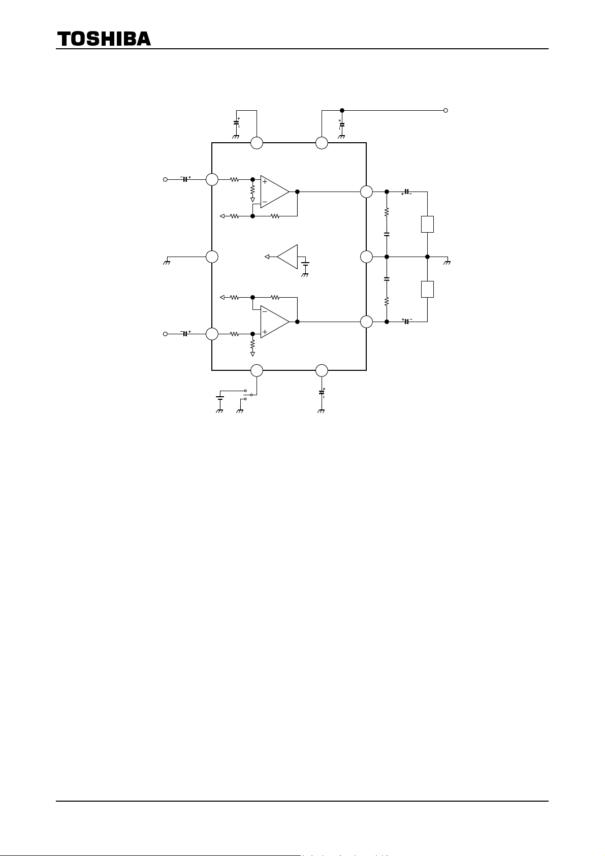
Block Diagram
INPUT1
RIPPLE FILTER
4 kΩ
4
6 9
Amp 1
30 kΩ
OUT1
TA8246AHQ
V
CC
8
R
L
R
L
INPUT2
3
2
350 Ω
350 Ω
4 kΩ
30 kΩ
20 kΩ
V
18
20 kΩ
Amp 2
MUTE SW
PW-GNDPre-GND
2.1 V
OUT2
75
MUTE T.C.
10
12
2
2004-07-12
Page 3
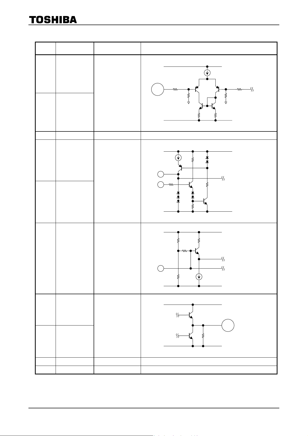
Terminal Explanation
A
TA8246AHQ
Terminal
No.
2 IN2
4 IN1
3 Pre-GND GND terminal ⎯
5 MUTE SW
Symbol Function Equivalent Circuit
4 kΩ
30 kΩ
Input
2/4
7
MUTE control terminal
5
10 kΩ
V
CC
NF へ
to MUTE
20 kΩ
350 Ω
GND
V
CC
mplifier
OUT
7 MUTE T.C.
10 kΩ
6 R/F Ripple filter
6
5.1 kΩ
8 OUT1
Output
12 OUT2
9 V
10 PW-GND GND terminal ⎯
CC
Supply voltage terminal ⎯
GND
to POP-NOIZE
preventive circuit
to Bias circuit
V
CC
8/12
2.2 kΩ
GND
1, 11: NC
3
2004-07-12
Page 4

TA8246AHQ
Cautions
This IC is not proof enough against a strong E-M field by CRT which may cause malfunction such as leak.
Please set the IC keeping the distance from CRT.
Maximum Ratings
Characteristic Symbol Rating Unit
(Ta = 25°C)
Supply voltage V
Output current (peak/ch) I
Power dissipation PD (Note) 25 W
Operating temperature T
Storage temperature T
CC
O (peak)
opr
stg
30 V
2 A
−20~75 °C
−55~150 °C
Note: Derated above Ta = 25°C in the proportion of 200 mW/°C.
Electrical Characteristics
(Unless otherwise specified, VCC = 20 V, RL = 8 Ω, Rg = 620 Ω, f = 1 kHz, Ta = 25°C)
Characteristic Symbol
Quiescent current I
Output power
Total harmonic distortion
Voltage gain G
Input resistance R
Ripple rejection ratio R.R. ⎯ f = 100 Hz −40 −47 ⎯ dB
Output noise voltage V
Cross talk C.T. ⎯
Mute control voltage
Mute attenuation level ATT ⎯ V
CCQ
P
(1) ⎯ THD = 10% 5 6 ⎯
out
(2) ⎯ THD = 1% ⎯ 4.5 ⎯
P
out
THD (1) ⎯ P
THD (2) ⎯ P
v
IN
no
V
th (ON)
V
th (OFF)
Test
Circuit
⎯ Vin = 0 50 85 130 mA
⎯ V
⎯ ⎯ ⎯ 34 ⎯ kΩ
Rg = 10 kΩ,
⎯
BW = 20 Hz~20 kHz
Rg = 10 kΩ,
V
⎯ MUTE ON 3.1 ⎯ V
⎯ MUTE OFF 0 ⎯ 2.5
Test Condition Min. Typ. Max Unit
= 2 W ⎯ 0.04 0.2
out
= 2 W, f = 10 kHz, ⎯ 0.1 0.6
out
= 0.775 Vrms 32.5 34 35.5 dB
out
⎯ 0.14 0.3 mVrms
= 0.775 Vrms
out
= 0.775 Vrms → Mute −52 −60 ⎯ dB
out
⎯ −60 ⎯ dB
CC
W
%
V
4
2004-07-12
Page 5

Test Circuit
TA8246AHQ
V
CC
INPUT1
INPUT2
1.0 µF
1.0 µF
100 µF
RIPPLE FILTER
4 kΩ
4
350 Ω
3
350 Ω
4 kΩ
2
6 9
Amp 1
30 kΩ
20 kΩ
V
18
20 kΩ
Amp 2
30 kΩ
5
MUTE SW
PW-GNDPre-GND
2.1 V
7
10 µF
1000 µF
OUT1
OUT2
MUTE T.C.
10
12
1000 µF
8
2.2 Ω
2.2 Ω
0.10 µF
0.10 µF
1000 µF
R
L
R
L
5
2004-07-12
Page 6

TA8246AHQ
t
200
(mA)
CCQ
VIN = 0
160
120
80
I
CCQ
40
Quiescent current I
0
4
0 12 8 16 20 24 32 28 36
Supply voltage VCC (V)
30
10
VCC = 20 V
= 8 Ω
R
L
5
3
1
0.5
0.3
Total harmonic distortion THD (%)
0.1
0.05
0.03
f = 10 kHz
f = 1 kHz
0.01
0.3
Output Power P
, V
out (DC)
THD – P
f = 100 Hz
– V
CC
V
ou
I
CCQ
20
16
12
8
4
0
(V)
out (DC)
Output voltage V
10
VCC = 20 V
5
P = 2 W
out
3
= 8 Ω
R
L
1
0.5
0.3
0.1
0.05
0.03
Total harmonic distortion THD (%)
0.01
30
Frequency f (Hz)
out
30 10 3 5 0.5 1
(W) Output Power P
out
30
f = 1 kHz
= 8 Ω
R
L
10
5
3
1
0.5
0.3
0.1
Total harmonic distortion THD (%)
0.05
0.03
0.01
0.3
THD – P
VCC = 12 V 28 20
1 3 5 10 30 0.5
THD – f
out
out
100 k30 k 10 k 3 k 1 k 100 300
(W)
6
2004-07-12
Page 7

TA8246AHQ
20
f = 1 kHz
18
R = 8 Ω
L
THD = 10%
16
14
(W)
out
12
10
8
6
Output power P
4
2
0
10 12 30 22 14 18 16 20 24 26 28 34 30
Supply voltage VCC (V) Frequency f (Hz)
0
VCC = 20 V
R = 8 Ω
L
−10
R = 0
g
= 0.775 Vrms
V
ripple
−20
−30
−40
−50
Ripple rejection ratio R.R. (dB)
−60
−70
30
Frequency f (Hz)
1.6
VCC = 20 V
)
rms
(mV
no
Output noise voltage V
= 8 Ω
R
1.4
L
BW = 20 Hz~20 kHz
1.2
1.0
0.8
0.6
0.4
0.2
0
30
100 300 1 k 3 k 10 k 30 k 100 k
Signal source resistance Rg (Ω)
P
out
R.R. – f
V
no
– V
– R
CC
G
– f
v
100 k30 k 10 k 3 k 1 k 100 300
32 36 38
70
VCC = 20 V
V = 0.775 Vrms
60
out
R
= 8 Ω
L
50
(dB)
v
40
30
20
Voltage gain G
10
0
C.T. – f
0
VCC = 20 V
R = 8 Ω
L
−10
V = 0.775 Vrms
out
= 10 kΩ
R
g
−20
−30
−40
−50
Cross talk C.T. (dB)
−60
100 k30 k 10 k 3 k 1 k 100 300 30
−70
100 k30 k 10 k 3 k 1 k 100 300
Frequency f (Hz)
g
0
VCC = 20 V
R = 8 Ω
L
−10
f = 100 Hz
ripple
= 0.775 Vrms
V
ripple
−20
−30
−40
−50
Ripple rejection ratio R.R. (dB)
−60
−70
30
Signal source resistance Rg (Ω)
R.R. – R
g
100 k30 k 10 k 3 k 1 k 100 300
7
2004-07-12
Page 8

TA8246AHQ
0
VCC = 20 V
f = 1 kHz
−10
R = 8 Ω
L
= 0.775 Vrms
V
out
−20
−30
−40
C.T. – R
g
−50
Cross talk C.T. (dB)
−60
−70
30
100 300 1 k 3 k 10 k 30 k 100 k
Signal source resistance Rg (Ω)
20
f = 1 kHz
18
RL = 8 Ω
16
MAX (W)
D
14
12
10
8
6
4
2
Maximum power dissipation P
0
8 32
Supply voltage VCC (V)
P
MAX – V
D
CC
24 28 16 2012
0.8
VCC = 20 V
0.7
= 10 kΩ
R
g
0.6
(mVrms)
no
0.5
0.4
0.3
0.2
0.1
Output noise voltage V
0
−40 100
Ambient temperature Ta (°C)
V
– Ta
no
40 60 0 20 −20
80
P
– P
D
18
Dual
f = 1 kHz
16
= 8 Ω
R
L
14
(W)
12
D
VCC = 28 V
10
8
20 V
6
4
Power dissipation P
12 V
2
0
0 8 10 1612
624
Output power P
out
THD = 1%
out
(W)
I
– Ta
180
VCC = 20 V
160
= 0
V
IN
140
(mA)
120
CCQ
100
80
60
40
Quiescent current I
20
0
−40 100
Ambient temperature Ta (°C)
CCQ
40 60 020−20
THD – Ta
10
VCC = 20 V
5
R
= 8 Ω
L
3
f = 1 kHz
P
= 2 W
out
Dual
1
0.5
0.3
0.1
0.05
0.03
Total harmonic distortion THD (%)
0.01
−40 100
Ambient temperature Ta (°C)
40 60 020−20 80
10%
14
80
8
2004-07-12
Page 9

TA8246AHQ
30
1
25
MAX (W)
D
20
2
15
3
10
5
Allowable power dissipation P
0
0 100 125 200150 75 25 50 175
Ambient temperature Ta (°C)
P
MAX – Ta
D
1: Infinite heat sink
2: 4.1°C/W heat sink
3: 9.5°C/W heat sink
9
2004-07-12
Page 10

Package Dimensions
TA8246AHQ
Weight: 4.04 g (typ.)
10
2004-07-12
Page 11

About solderability, following conditions were confirmed
• Solderability
(1) Use of Sn-63Pb solder Bath
· solder bath temperature = 230°C
· dipping time = 5 seconds
· the number of times = once
· use of R-type flux
(2) Use of Sn-3.0Ag-0.5Cu solder Bath
· solder bath temperature = 245°C
· dipping time = 5 seconds
· the number of times = once
· use of R-type flux
TA8246AHQ
RESTRICTIONS ON PRODUCT USE
• The information contained herein is subject to change without notice.
• The information contained herein is presented only as a guide for the applications of our products. No
responsibility is assumed by TOSHIBA for any infringements of patents or other rights of the third parties which
may result from its use. No license is granted by implication or other wise under any patent or patent rights of
TOSHIBA or others.
• TOSHIBA is continually working to improve the quality and relia bility of its products. Nevertheless, semiconductor
devices in general can malfunction or fail due to their inherent e lectrical sensitivity and vulnerability to physical
stress. It is the responsibility of the buyer, when utilizing TOSHIBA products, to comply with the standards of
safety in making a safe design for the entire system, and to avoid situations in which a malfunction or failure of
such TOSHIBA products could cause loss of human life, bodily injury or damage to property.
In developing your designs, please ensure that TOSHIBA products are use d within specified operating ra nges as
set forth in the most recent TOSHIBA products specifications. Also, please keep in mind the precautions and
conditions set forth in the “Handling Guide for Semiconductor Devices,” or “TOSHIBA Semiconductor Reliabilit y
Handbook” etc..
• The TOSHIBA products listed in this document are intended for usage in general electronics applications
(computer, personal equipment, office equipment, measuring equipment, industrial robotics, domestic appli ances,
etc.). These TOSHIBA products are neither intended nor warranted for usage in equipment that requires
extraordinarily high quality and/or reliability or a malfunction or failure of which may cause loss of hum an life or
bodily injury (“Unintended Usage”). Unintended Usage include atomic energy control instruments, airplane or
spaceship instruments, transportation instruments, traffic signal instruments, combustion control instruments,
medical instruments, all types of safety devices, etc.. Unintended Usage of TOSHIBA products listed in this
document shall be made at the customer’s own risk.
030619EBF
• The products described in this document are subject to the foreign exchange and foreign trade laws.
• TOSHIBA products should not be embedded to the downstream product s which are prohibited to be produced
and sold, under any law and regulations.
• This product generates heat during normal operation. However, substandard performance or malfunction may
cause the product and its peripherals to reach abnormally high temperatures.
The product is often the final stage (the external output stage) of a circuit. Substandard performance or
malfunction of the destination device to which the circuit supplies output may cause damage to the circuit or to the
product.
11
2004-07-12
 Loading...