

TOSHIBA SSM6N15FU Datasheet

TOSHIBA Field Effect Transistor Silicon N Channel MOS Type
SSM6N15FU
SSM6N15FU
High Speed Switching Applications
Analog Switching Applications
• Small package
• Low ON resistance : R
: R
Absolute Maximum Ratings
(Q1, Q2 Common)
Characteristics Symbol Rating Unit
Drain-Source voltage V
Gate-Source voltage V
Drain current
Drain power dissipation (Ta = 25°C) PD (Note 1) 200 mW
Channel temperature Tch 150 °C
Storage temperature range T
= 4.0 Ω (max) (@VGS = 4 V)
on
= 7.0 Ω (max) (@VGS = 2.5 V)
on
(Ta = 25°C)
DS
±20 V
GSS
DC ID 100
Pulse I
200
DP
−55 to 150 °C
stg
30 V
mA
Unit: mm
JEDEC ―
JEITA ―
Note: Using continuously under heavy loads (e.g. the application of
high temperature/current/voltage and the significant change in
temperature, etc.) may cause this product to decrease in the
reliability significantly even if the operating conditions (i.e.
operating temperature/current/voltage, etc.) are within the absolute maximum ratings.
Please design the appropriate reliability upon reviewing the Toshiba Semiconductor Reliability Handbook
(“Handling Precautions”/“Derating Concept and Methods”) and individual reliability data (i.e. reliability test
report and estimated failure rate, etc).
Note 1: Total rating
Marking Equivalent Circuit
6 5 4
6 5 4
Q1
D P
1 2 3
1 2 3
(top view)
Q2
Handling Precaution
TOSHIBA 2-2J1C
Weight: 6.8 mg (typ.)
When handling individual devices (which are not yet mounting on a circuit board), be sure that the environment
is protected against electrostatic electricity. Operators should wear anti-static clothing, and containers and other
objects that come into direct contact with devices should be made of anti-static materials.
Start of commercial production
2001-02
1
2014-03-01
SSM6N15FU
)
Electrical Characteristics
Characteristics Symbol Test Condition Min Typ. Max Unit
Gate leakage current I
Drain-Source breakdown voltage V
Drain cut-off current I
Gate threshold voltage Vth VDS = 3 V, ID = 0.1 mA 0.8 ⎯ 1.5 V
Forward transfer admittance ⎪Yfs⎪ VDS = 3 V, ID = 10 mA 25 ⎯ ⎯ mS
Drain-Source ON resistance R
Input capacitance C
Reverse transfer capacitance C
Output capacitance C
Switching time
Turn-on time t
Turn-off time t
(Ta = 25°C) (Q1, Q2 Common)
VGS = ±16 V, VDS = 0 ⎯ ⎯ ±1 μA
GSS
(BR) DSSID
DSS
DS (ON)
⎯ 7.8 ⎯ pF
iss
⎯ 3.6 ⎯ pF
rss
oss
⎯ 50 ⎯
on
off
= 0.1 mA, VGS = 0 30 ⎯ ⎯ V
VDS = 30 V, VGS = 0 ⎯ ⎯ 1 μA
ID = 10 mA, VGS = 4 V ⎯ 2.2 4.0
= 10 mA, VGS = 2.5 V ⎯ 4.0 7.0
I
D
V
= 3 V, VGS = 0, f = 1 MHz
DS
V
= 5 V, ID = 10 mA,
DD
= 0 to 5 V
V
GS
⎯ 8.8 ⎯ pF
⎯ 180 ⎯
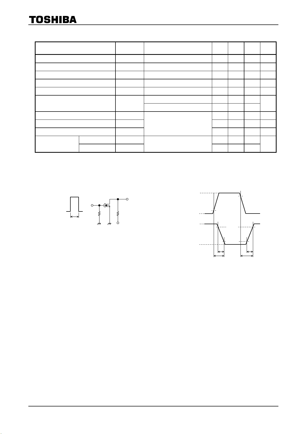
Switching Time Test Circuit
(a) Test circuit
(b) V
IN
Ω
ns
V
DS (ON
V
5 V
0 V
DD
10%
t
t
on
90%
10%
90%
r
t
f
t
off
5 V
0
10 μs
VDD = 5 V
Duty ≤ 1%
V
: tr, tf < 5 ns
IN
= 50 Ω)
(Z
out
Common Source
Ta = 25°C
OUT
IN
L
50 Ω
R
V
DD
(c) V
OUT
Precaution
Vth can be expressed as voltage between gate and source when low operating current value is ID = 100 μA for this
product. For normal switching operation, V
voltage than V
. (Relationship can be established as follows: V
th
Please take this into consideration for using the device.
requires higher voltage than Vth and V
GS (on)
< Vth < V
GS (off)
GS (on)
)
requires lower
GS (off)
2
2014-03-01
 Loading...