Toshiba SD-V55HTSU, SD-V55HTSC Service Manual

CIRCUIT DIAGRAMS
DVD/VCR
Home Theater System
FILE NO. 810-200425
SD-V55HTSU
SD-V55HTSC
DOCUMENT CREATED IN JAPAN, May, 2004

3-1
SECTION 3
ELECTRICAL
CONTENTS
OVERALL WIRING DIAGRAM .............................3-2
VCR PART
ELECTRICAL ADJUSTMENT
PROCEDURES ...........................................................3-3
ELECTRICAL TROUBLESHOOTING
GUIDE ............................................................................3-4
1. POWER(SMPS) CIRCUIT.......................................3-4
2. SYSTEM/KEY CIRCUIT..........................................3-6
3. SERVO CIRCUIT ....................................................3-7
4. OSD CIRCUIT .........................................................3-9
5. Y/C CIRCUIT.........................................................3-10
6. TUNER/IF CIRCUIT ..............................................3-14
7. Hi-Fi CIRCUIT.......................................................3-16
BLOCK DIAGRAMS ...............................................3-18
1. POWER(SMPS) BLOCK DIAGRAM 1 .................3-18
2. POWER(SMPS) BLOCK DIAGRAM 2 .................3-20
3. Y/C BLOCK DIAGRAM ........................................3-22
4. NORMAL AUDIO BLOCK DIAGRAM..................3-24
5. Hi-Fi BLOCK DIAGRAM ......................................3-26
6. SYSTEM BLOCK DIAGRAM ...............................3-28
CIRCUIT DIAGRAMS .............................................3-30
1. POWER(SMPS) CIRCUIT DIAGRAM 1 ...............3-30
2. POWER(SMPS) CIRCUIT DIAGRAM 2 ...............3-32
3. JACK/TUNER CIRCUIT DIAGRAM .....................3-34
4. A/V CIRCUIT DIAGRAM.......................................3-36
5. Hi-Fi CIRCUIT DIAGRAM ....................................3-38
6. SYSTEM CIRCUIT DIAGRAM..............................3-40
7. KEY CIRCUIT DIAGRAM .....................................3-42
• WAVEFORMS.........................................................3-44
• CIRCUIT VOLTAGE CHART..................................3-46
PRINTED CIRCUIT DIAGRAMS ........................3-48
1. MAIN P.C.BOARD ................................................3-48
2. POWER P.C.BOARD............................................3-50
3. KEY 1(LEFT) P.C.BOARD....................................3-52
4. KEY 2(RIGHT) P.C.BOARD..................................3-52
DVD & AMP PART
ELECTRICAL TROUBLESHOOTING
GUIDE ..........................................................................3-54
1. SYSTEM OPERATION FLOW..............................3-54
2. TEST & DEBUG FLOW........................................3-55
3. AUDIO µ-COM CIRCUIT(DVD & AMP)................3-63
DETAILS AND WAVEFORMS ON
SYSTEM TEST AND DEBUGGING ..................3-62
1. SYSTEM 27MHZ CLOCK,
RESET, FLASH R/W SIGNAL..............................3-62
2. SDRAM CLOCK ...................................................3-64
3. TRAY OPEN/CLOSE SIGNAL..............................3-64
4. SLED CONTROL RELATED SIGNAL
(NO DISC CONDITION)........................................3-66
5. LENS CONTROL RELATED SIGNAL
(NO DISC CONDITION)........................................3-66
6. LASER POWER CONTROL RELATED
SIGNAL(NO DISC CONDITION) ..........................3-67
7. DISC TYPE JUDGEMENT WAVEFORMS ...........3-67
8. FOCUS ON WAVEFORMS...................................3-69
9. SPINDLE CONTROL WAVEFORMS
(NO DISC CONDITION)........................................3-70
10. TRACKING CONTROL RELATED
SIGNAL(SYSTEM CHECKING) .........................3-71
11. RF WAVEFORM..................................................3-72
12. MT1379 VIDEO OUTPUT WAVEFORMS...........3-72
13. AUDIO OUTPUT FROM AUDIO DAC ................3-74
14. DVD & AMP WAVEFORMS................................3-75
BLOCK DIAGRAMS ...............................................3-76
1. OVERALL BLOCK DIAGRAM .............................3-76
2. SERVO BLOCK DIAGRAM..................................3-77
3. MPEG & MEMORY BLOCK DIAGRAM...............3-78
4. VIDEO & AUDIO BLOCK DIAGRAM...................3-79
5. DVD & AMP BLOCK DIAGRAM..........................3-80
CIRCUIT DIAGRAMS .............................................3-81
1. MPEG CIRCUIT DIAGRAM..................................3-81
2. RF & SERVO CIRCUIT DIAGRAM ......................3-83
3. AUDIO, µ-COM
CIRCUIT DIAGRAM(DVD & AMP).......................3-85
4. DIGITAL AMP CIRCUIT
DIAGRAM (DVD & AMP)......................................3-87
5. PWM & CODEIC
CIRCUIT DIAGRAM (DVD & AMP)......................3-89
6. INTERFACE
CIRCUIT DIAGRAM (DVD & AMP)......................3-91
• CIRCUIT VOLTAGE CHART..................................3-93
PRINTED CIRCUIT DIAGRAMS ........................3-97
1. DVD & AMP P.C.BOARD .....................................3-97
3-2
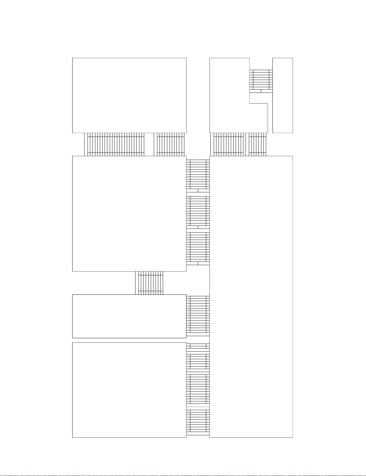
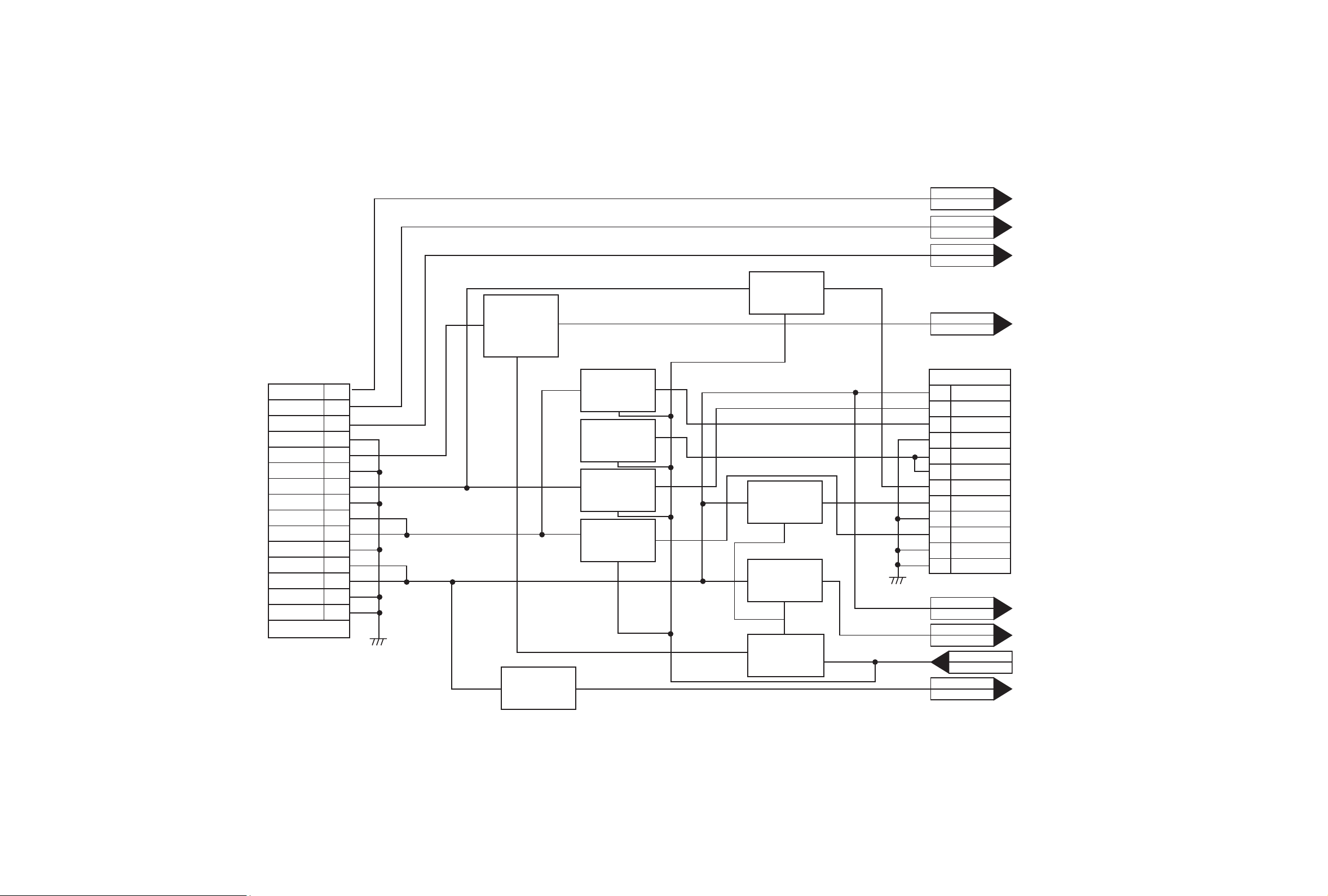
OVERALL WIRING DIAGRAM
PMC01
CFG
CAP Vcc
5.2VA
CAP REV’H’
V-limit
MOTOR GND
S.GND
DRUM(L/M)Vcc
CAP CTL
L/M CONTROL
DPG/FG
DRUM CTL
1
2
3
4
5
6
7
8
9
10
11
12
1
2
3
4
5
6
7
8
9
10
11
12
P3D01
SP PB A
SP REC
SP PB B
EP PB B
EP REC
EP PB A
HiFi PB A
HiFi REC
HiFi PB B
1
2
3
4
5
6
7
8
9
1
2
3
4
5
6
7
8
9
PVS01 PSV01
GND
GND
5.3VA
5.3VA
GND
3.8VA
3.8VA
GND
13VA
GND
33VA
GND
-29VA
FD(-)
FD(+)
1
2
3
4
5
6
7
8
9
10
11
12
13
14
15
1
2
3
4
5
6
7
8
9
10
11
12
13
14
15
PSW01
32VA
32VA
32VA
32VA GND
32VA GND
32VA GND
NC
GND
NC
PWR SENSE
123456789
10
123456789
10
PDM01
H FM_VCC
RF_VCC
LD_DVD
MD_DVD
VR_DVD
GND_PD
VRBF
VC
F
B
A
D
C
B
FOCUS+
TRACKING-
TRACKING+
FOCUS-
SW_PDIC
GND_LCD
LD_CD
MD_CD
VR_CD
123456789
10111213141516171819202122
23
123456789
10111213141516171819202122
23
PV601 P6M01
KEY RETURN 1
KEY RETURN 2
5.3VA
VIDEO IN
GND
AUDIO ’L’ IN
GND
AUDIO ’R’ IN
GND
FD(-)
-27VA
FD(+)
123456789
101112
123456789
101112
PV602 P6M02
REMOCON
GND
FLD CLOCK
FLD DATA
FLD ENA
VOLUME DOWN
VOLUME UP
1234567
1234567
PDM03
SPM -
SPM +
FM -
FM +
LM -
LM +
SW(OPEN)
SW(CLOSE)
GND
SW(LOADIN)
GND
123456789
10
11
123456789
10
11
P3D02
CTL(+)
CTL(-)
A/E(+)
A/E(-)
A.REC
A.PB
1
2
3
4
5
6
1
2
3
4
5
6
GND
FULL ERASE
P3D03
1
2
1
2
5.3VA
NC(-9V)
REG 8V(M)
GND(M)
REG 9V(+9V)
A. GND
REG 3.3V
5V
D. GND
REG 3.3V
A.GND
D.GND
PDV02PVD01
1
2
3
4
5
6
7
8
9
10
11
12
1
2
3
4
5
6
7
8
9
10
11
12
DVD V.IN
GND
DVD A.L IN
GND
DVD A.R IN
GND
VCR A.L OUT
VCR A.R OUT
GND
Pb/B
Y/G
Pr/R
PDV02PVD02
1
2
3
4
5
6
7
8
9
10
11
12
1
2
3
4
5
6
7
8
9
10
11
12
DVD ENA
GND
DVD DATA OUT
DVD DATA IN
DVD CLOCK
DVD RESET
AMP DATA IN
AMP CLOCK
GND
AMP ENA
AMP DATA OUT
AMP RESET
PDV02PVD02
1
2
3
4
5
6
7
8
9
10
11
12
1
2
3
4
5
6
7
8
9
10
11
12
GND(D)
KEY RTN 1
GND(A)
F.A.R.IN
GND(A)
F.A.L.IN
GDN(D)
VIDEO IN
P6602P6603
1
2
3
4
5
6
7
8
1
2
3
4
5
6
7
8
DECK MD
MPEG/AMP
BOARD
SMPS
BOARD
TIMER
BOARD
KEY BOARD
VCR
3-3
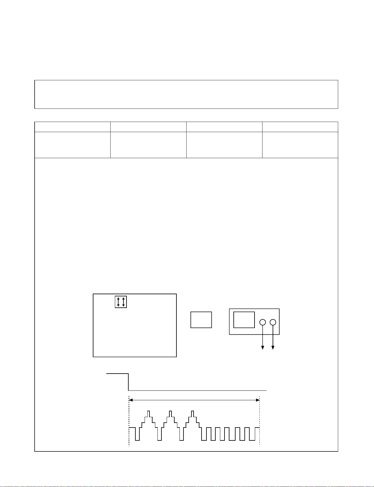
ELECTRICAL ADJUSTMENT PROCEDURES
1. Servo Adjustment
1) PG Adjustment
• Adjustment And Specification
• Test Equipment
a) OSCILLOSCOPE
b) NTSC MODEL : NTSC SP TEST TAPE
MODE
PLAY
• Adjustment Procedure
a) Insert the SP Test Tape and play.
b) Press the “O” key on the Remote controller and the “PLAY” key on the Front Panel the same time, the
unit then goes in to Tracking initial mode.
c) Trigger the mixed Combo Video Signal of CH2 to the CH1 H/SW(W373, W374), and then check the dis-
tance (time difference), which is from the selected A(B) Head point of the H/SW(W373, W374) signal to
the starting point of the vertical synchronized signal, to 6.5H ± 0.5H (412µs, 1H=63µs).
Note - Press FRONT CH UP KEY and FRONT PLAY KEY on Deck playback, and it goes in to ATR PRE-
SET. after the SP Test Tape is inserted.
• PG Adjustment Method
a-1) Playback the SP standard tape
b-2) Press the “O” key on the Remote controller and the “PLAY” key on the Front Panel the same time,
Tracking initial mode.
c-3) Repeat the above step(No.b-2), the unit will then finish the PG adjusting automatically.
d-4) Stop the playback, the unit then exits PG adjusting mode after saving the PG data.
• CONNECTION
• WAVEFORM
V.Out
H/SW(W373, W374)
R/C TRK JIG KEY 6.5 ± 0.5H
MEASUREMENT POINT ADJUSTMENT POINT SPECIFICATION
V.Out
H/SW(W373, W374)
OSCILLOSCOPE
CH1 CH2
V.outH/SW
R/C KEY
(W373, W374)
H/SW
Composite
VIDEO
6.5H(412µs)
VCR PART

3-4
ELECTRICAL TROUBLESHOOTING GUIDE
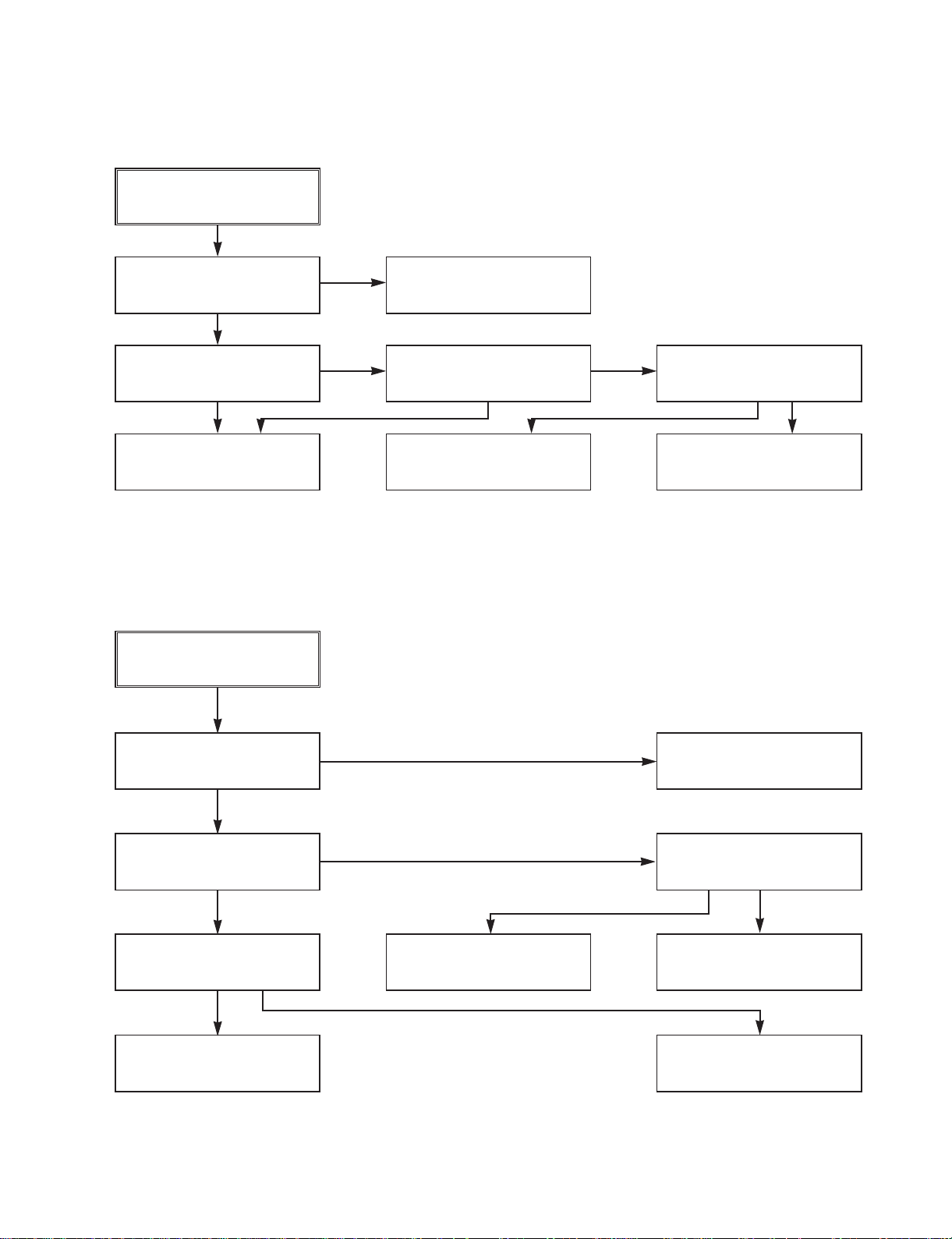
1. Power(SMPS) CIRCUIT
NO 5.3VA.
Replace the F101.
(Use the same Fuse)
Is the F101 normal?
Is the TH101
normal?
Is the BD101
normal?
NO
NO
NO
NO
NO
NO
Replace the
BD101.
Replace the TH101.
Is the D105
normal?
Check or Replace
the D105.
Replace the D129.
Replace the IC106.
YES
YES
YES
YES
YES
YES
YES
Is Vcc(8.5~21V) supplied to IC104 Pin3?
NO
Is the D129
normal?
Is there about 2.5V
at the IC106 Vref?
Check the Main PCB
5.3VA/5.0V Line short?
(1) No 5.3VA (SYS/Hi-Fi/TUNER)
NO 12VA.
Check or Replace
the D126.
Is the Vcc(13V) supplied
to (+) terminal in D126?
Check or Replace
the Motor Vcc.
NO
YES
YES
(2) No 12VA (TO CAP, DRUM MOTOR)
NO 5.0VA.
5.3VA Line Check.
Is 5.3VA put into
the Q167 Emitter?
Is about 5V put into
the Q167 Base?
Is the Q169 Base
“H”?
NO
NO
Check the Power
Control.
NO
Check or Replace the
Q169, R175, R176, R177.
YES
YES
YES
Check or Replace
the Q167/Q169.
YES
(3) No 5.0V (SYS/Hi-Fi/TUNER)

3-5
NO 5V.
5.3VA Line Check.
Is 5.3VA put into
the Q168 Emitter?
Is about 5V put into
the Q168 Base?
Is the Q169 Base
“H”?
NO
NO
NO
Check the Power
Control.
Check or Replace the
Q169, R175, R176, R177.
YES
YES
YES
YES
Check or Replace
the Q168/Q169
(4) No 5V (TO DVD)
No 33V.
Check the Power
Control.
Is Q163 Base “H”?
Check or Replace
Q163, R168, R169.
NO
YES
YES
(5) No 33V (TUNER)
NO 8V.
Check or Replace
the D126.
Is Vcc(13V) supplied to
(+) terminal in D126?
Check or Replace
IC161, C163.
Is Vcc(12V) supplied
to IC160 Pin1?
NO
NO
Check or Replace
the D163.
YES
YES
YES
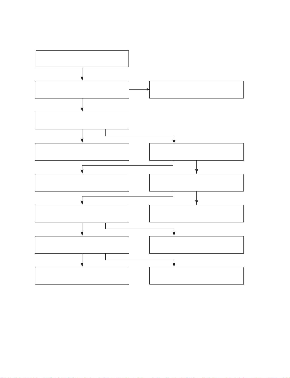
(6) No 8V(TO DVD)
3-6
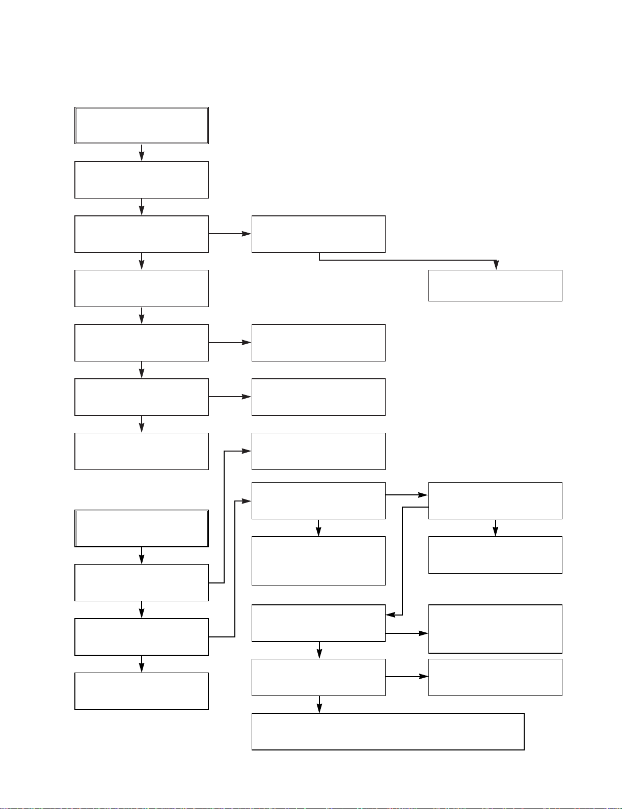
2. SYSTEM/KEY CIRCUIT
(1) AUTO STOP
(2) The unstable loading of a Cassette tape
Auto Stop
Does the SW30 waveform
appear at the IC501
Pin18?
Do the T-UP Reel Pulses
appear at the IC501 Pin80?
Is 12V applied to the
PMC01 Pin8?
Check the Drum Motor
signal.
Does 5V appear at the
RS501?
Check the Q160 Power
Circuit.
Refer to “SMPS DRUM
12 Volt Trouble Shooting”.
Is 5V applied to the
R531 ?
Refer to SMPS 5.3VA
troubleshooting.
Check the IC501
Pins22, 23, 24, 25.
Do T/UP Reel Pulses
appear at the point
between R556 and R536?
Replace the T/UP Reel
Sensor (RS501).
Check the CST SW and
the peripheral circuitry.
Replace the IC501.
The unstable loading of a
Cassette tape
Does the “H” signal appear
at the IC501 Pin58 during
inserting the CST ?
Does the “L” signal appear
at the IC501 Pin60 during
inserting the CST?
Check the Deck
Mechanism.
Caution :
Auto stop can occur because Grease or Oil has dried up
YES
YES
YES
NO
YES
YES
YES
YES
NO
NO
NO
NO
NO
NO NO
YES
YES YES
3-7
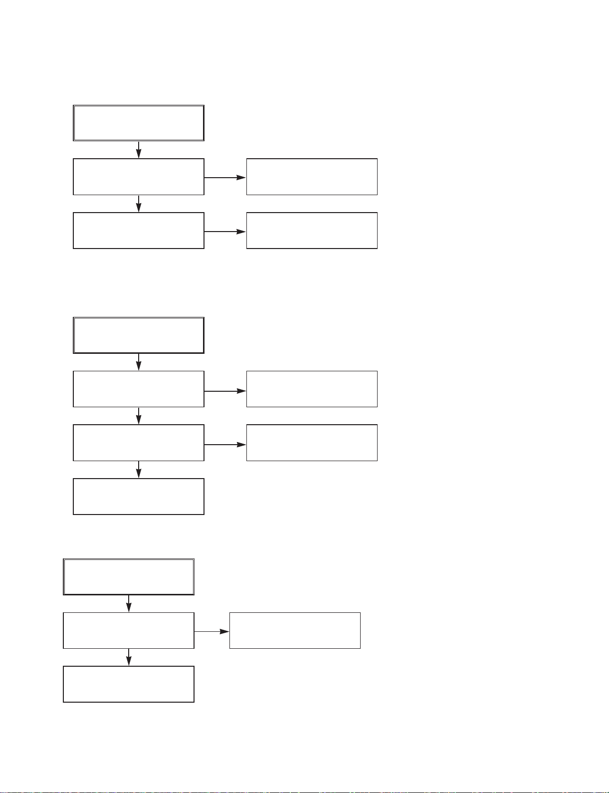
3. SERVO CIRCUIT
(1) Unstable Video in PB MODE
Unstable Video in
PB Mode.
Does the Noise level of the
screen change
periodically?
Do the CTL pulses appear
at the IC501 Pin97?
Is adjusting the height of
the CTL Head accurate?
Readjust the height of the
CTL Head.
Replace the IC501.
Refer to “When the Y signal
doesn’t appear on the
screen in PB Mode”.
Does the CFG waveform
appear at the IC501
Pin87?
On tracking do the CTL
pulses move?
Does the Video Envelope
waveform appear at the
IC501 Pin9?
Replace the IC501.
YES
YES
YES
YES
YES
YES
NO
NO
NO
NO
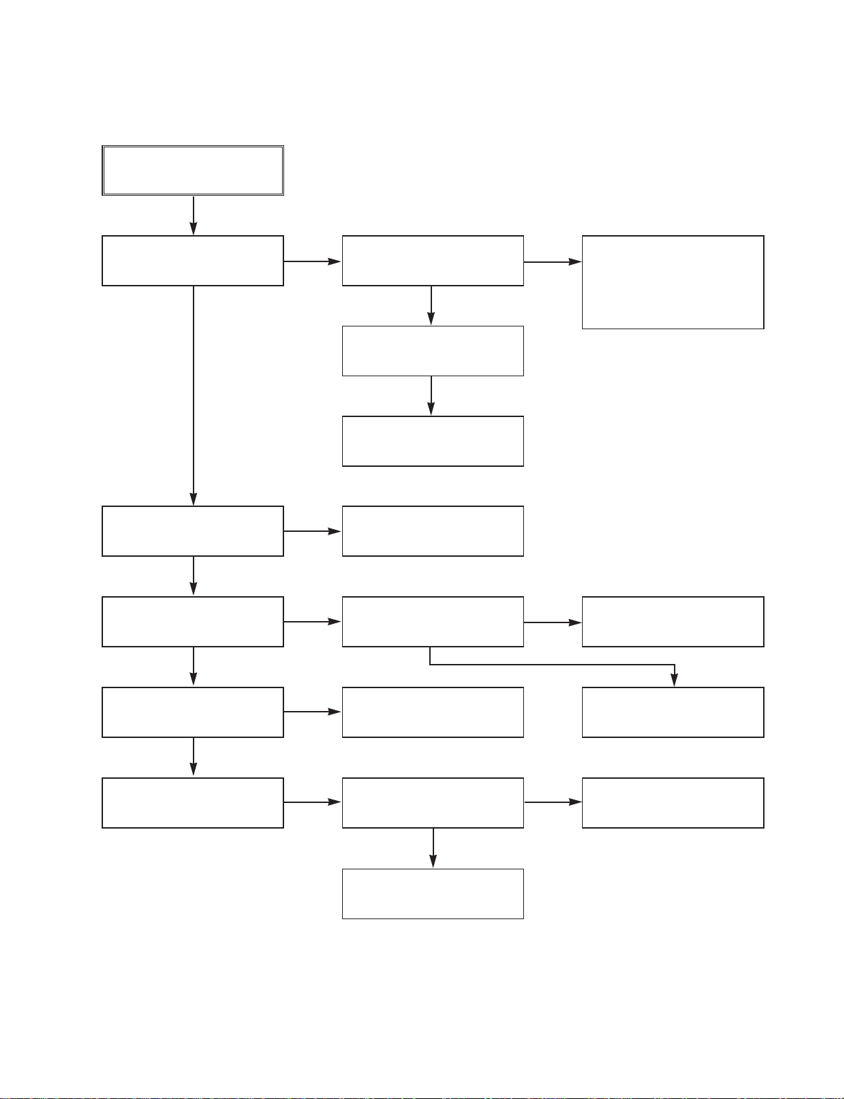
(2) When the Drum Motor
(2) doesn’t run.
Do the DFG Pulses appear
at the PMC01 Pin11?
Replace the Cap M.
Aren’t the foil patterns and
the Components between
IC501 Pin 90 and PMC01
Pin11 short?
Replace the IC501.
Refer to “(2)
No 12VA of Power section”
Do the Drum PWM Pulses
appear at the IC501
Pin76?
Aren’t the foil patterns and
the Components between
IC501 Pin76 and PMC01
Pin12 short?
Do the DFG Pulses appear
at the IC501 Pin90?
Do the Drum PWM Pulses
appear at the IC501
Pin76?
Aren’t the connecting patterns and the Components
between IC501 Pin76 and PMC01 Pin12 short?
When the Drum Motor
doesn’t run,
Does 12V appear at the
PMC01 Pin8?
Does 2.8V appear at the
PMC01 Pin12?
Check the connector
(PMC01) and the Drum
Motor Ass’y.
NO
YES
YES
YES
NO
NO
NO
NO
NO
YES
YES
YES
3-8
Does the CFG signal appear at the
PMC01 Pin1?
Does the PWM signal appear at the
IC501 Pin77?
Is “DRUM CTL” 2.8V appear at the
PMC01?
Check the PMC01 and the Capstan
Motor Ass’y.
Does the Capstan PWM signal appear at
the IC501 Pin77?
Aren’t the foil patterns and Components
between IC501 Pin77 and PMC01
Pin9 short?
Does the CFG signal come into the
IC501 Pin87?
Aren’t the foil patterns and Components
between IC501 Pin77 and PMC01
Pin9 short?
2. SERVO CIRCUIT
(3) When the Capstan Motor doesn’t run,
NO
NO
NO
YES
YES
YES
When the Capstan Motor doesn’t run,
Does 12VA appear at the PMC01?
YES
Replace the IC501.
YES
NO
NO
YES
Refer to “SMPS(CAPSTAN/12Volt)
Trouble Shooting”.
Aren’t the foil patterns and component
between IC501 Pin87 and PMC01
Pin1 short?
Check the Capstan Motor Ass’y.
NO
3-9
4. OSD CIRCUIT
(1) No OSD display.
(2) I2C BUS CHECK
KEY doesn’t working.
Is 5V applied to the IC501
Pin2, 3?
Does LED or FLD change
when a function button is
pressed?
No OSD or F.OSD display.
Is 5.3V applied to the
IC501 Pin53?
Does oscillation occur at
the IC501 Pins44, 45?
Replace the IC501.
The I2C waves don’t
come out.
Does Power appear at the
Pull up impedence
(R569, R507)?
Replace the IC501.
Refer to “SMPS 5.3VA
Trouble Shooting”.
Replace the defective
switches.
Refer to “SMPS 5.3VA
Trouble Shooting”.
Check or Replace the pheripheral Circurity.(L511,
R598, C596, C595)
Refer to “SMPS 5.3VA
Trouble Shooting”.
YES
YES
YES
YES
NO
NO
NO
NO
NO
2. SERVO CIRCUIT
(4) KEY doesn’t working
3-10
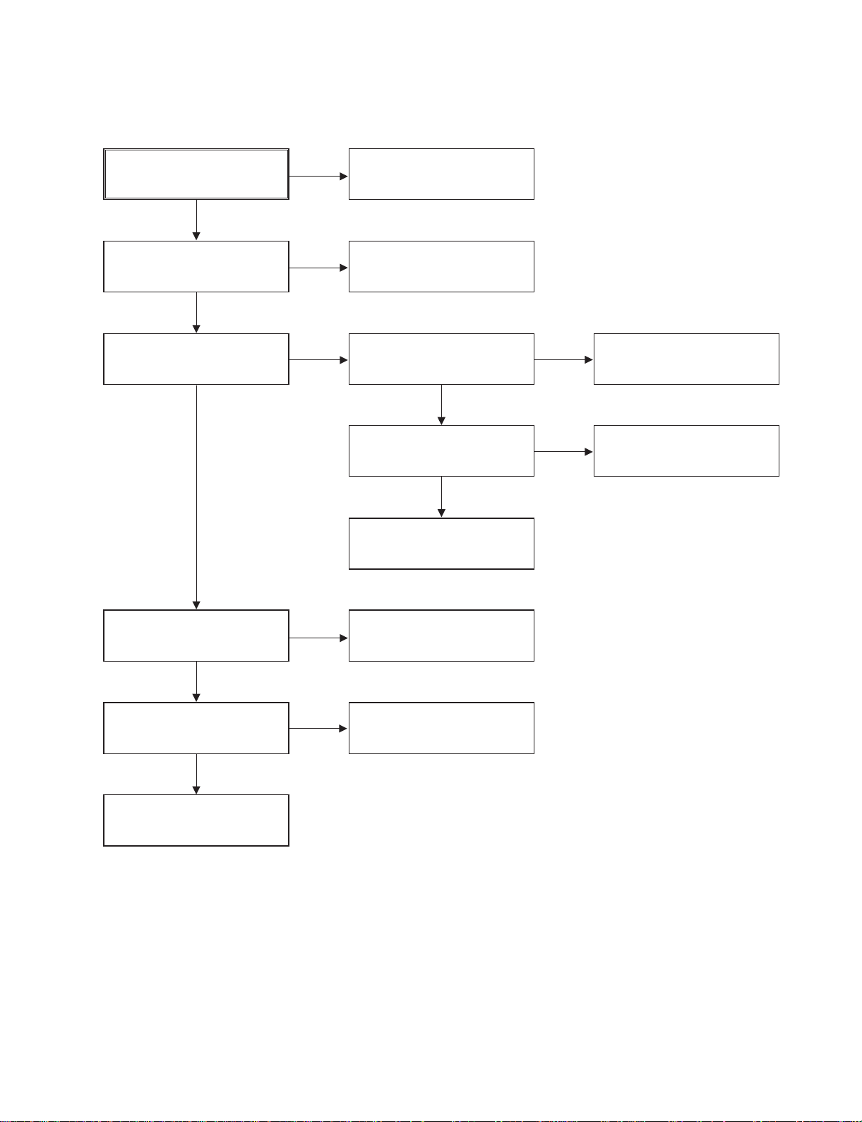
5. Y/C CIRCUIT
(1) No Video in EE Mode,
No Video in EE Mode
Does the Video signal
appear at the IC302
Pins1, 5?
Is there 5V at the IC302
Pin6?
Replace the IC302.
Does the Video signal
appear at the IC301
Pins28, 30, 32?
Is REG 5.0V applied to the
IC301Pins23, 44, 45, 52, 68,
77?
Does the Video signal
appear at the IC301 Pin26?
Does the Video signal
appear at the IC501 Pin52?
Does the Video signal
appear at the IC602 Pin7?
Check the REG 5V Line.
(Power Circuit)
Is I2C BUS signal applied to
the IC301 Pins53, 54, 55?
Replace the IC301.
Check the path of the signal between the IC301 Pin
26 and IC501 Pins50, 52.
Is there 5V on the plus
terminal of the C614?
Check the REG 5V Line.
(Power Circuit)
Replace the IC602.
Check the System Circuit.
(Refer to ‘SYSTEM I2C BUS
CHECK Trouble Shooting’)
YES
YES
YES
YES
YES
YES
NO
NO
NO
NO
NO
NO
NO
YES
YES
Check DVD Video Input
(IC602, Pin4), Tuner Video
Input (TU701 Pin16), Line
Video Input (JK601),
respectively.
NO
3-11
3. Y/C CIRCUIT
(2) When the Y(Luminance) signal doesn’t appear on the screen in PB Mode,
Is 5V applied to the IC301
Pins23, 44, 45, 52, 68, 77?
Is the Y/C Bus siganl
applied to the IC301
Pins53, 54, 55?
Does the normal RF signal
appear at the IC301 Pin 14?
Check the line of the REG
5V Line. (Power Circuit)
Check the System Circuit.
(IC501 Pin18)
Check the V.H.S/W level.
Refer to ‘SYSTEM Y/C
BUS CHECK Trouble
Shooting’.
Is the V.H.S/W signal
applied to the IC301 Pin57?
Does the Rectangular
waveform(5V) appear at
the IC301 Pin57(V.H.S/W)
Clean the Drum.
Check the C324.
Check the R328, R347,
C322, C323.
Does the Y(Luminance)
signal appear at the IC301
Pin20?
Is the Y(Luminance) Video
waveform showed up at the
IC301 Pin22?
Replace the IC301.
NO
YES
YES
YES
YES
YES
YES
YES
NO
NO
NO
NO
NO
NO

3-12
3. Y/C CIRCUIT
(3) When the C(Color) signal doesn’t appear on the screen in PB Mode,
Is 5V applied to the IC301
Pins23, 44, 45, 52, 68, 77?
Does the fsc signal appear
at the IC301 Pins41, 50?
Check the line of the REG
5V Line. (Power Circuit)
Replace the X301.
Check the C342, C341,
R333.
Is normal the X301
(3.58MHZ) of oscillation
Frequency?
Replace the IC301.
Does the Color signal
appear at the IC301 Pin48?
Replace the IC301.
NO
YES
YES
YES
NO
NO
NO
3-13
3. Y/C CIRCUIT
(4) When the Video signal doesn’t appear on the screen in REC Mode,
YES
YES
YES
YES
YES
YES
NO
NO
YES
YES
YES
YES
YES
Check system part
(V.H/SW)
Replace the IC301.
Check the drum
*OPTION
Pins72, 73, 74(SP)
Pins65, 66, 67(EP)
REC mode
Check the EE mode
NO
Is EE mode normal?
Is color
normal?
A
A
YES YES
Is brightness normal?
Does signal appear at
IC301 Pins41, 50?
NO
Check X301 oscillation
frequency.
YES
Is the brightness signal supplied to IC301 Pins18?
Is 5V supplied to IC301
Pins23, 44, 45, 68, 77?
Check the power of Pins23,
44, 45, 52, 68, 77.
Check the 5V power
NO
NO
NO
NO
NO
Is Y/C Bus applied to
IC301 Pins53, 54, 55?
Check the REG 5V power
Check system part
Do X301 and X-TAL
oscillate?
Check X301.
Is V.H SW supplied to
IC301 Pin57?
Does the FM signal appear
at IC301 Pins73(SP)/
66(EP)?
3-14
6. Tuner/IF CIRCUIT
(1) No Picture on the TV screen
No picture on the TV
screen
Does the Video signal at
the TU701 Pin16.
YES
YES YES
Is +33V applied to TU701
Pin14?
YES
Is +5V applied to TU701
Pin3?
NO
Does the video signal
appear at IC302 Pin7.
NO
Does the Video signal at
the IC501 Pin 52.
YES
NO
Does the Video signal at
the IC602 Pin 7.
YES
NO
Check the signal flow from IC602
Pin7 to JK601 Pin Video out.
YES
Check 33V line.
NO
Check 5V line.
NO
YES
Does the Clock signal
appear at TU701 Pin9?
Check the lIC Clock Signal
of µ-COM Pin71.
NO
YES
Does the data signal
appear at TU701 Pin10?
Replace Tuner.
Check the signal flow from
IC501 Pin27.(Pin27 is ‘L’
state in Tuner Mode)
Check the signal from IC301
Pin26 to IC501 Pin50.
Check the signal from IC501 Pin52 to IC602 Pin1 and IC602 Pin2.
(IC602 Pin2 is ‘L’ state in VHS mode)
Check the lIC Data Signal
of µ-COM Pin72.
NO

3-15
(2) No Sound
No Sound.
Check the Vcc of TU701 Pins3, 14.
YES
Check 5.2V, 33V Line.
NO
Check the Tuner SiF signal at IC801
Pin57.
YES
Check the Audio of IC801 Pins78, 80.
YES
Check the Signal flow from IC801 Pins78,
80 to JK601 Audio out(L), (R)
YES
Check the Tuner SIF of TU701 Pin13.
NO
1. Check the Vcc(5.3VA, 9V) of IC801
Pins3, 5, 36, 54.
2. Check the IIC Clock and Data at IC801
Pins37, 38.
NO
3-16
Check power.
Check REC start “H” signal
of µ-COM.
Check IC501 Pin 19.
(Audio Swich 30)
Check the Vcc of IC801.
(Pins 3, 15, 32, 46)
Is Pin 30 of IC801 over
3.5V ?
Is the Head switching signal
IC801 Pin 39 O.K?
Check the connection at
P3D01 if good then
Replace IC801.
Check Ports of µ-COM.
Check A.MUTE port of
µ-COM (Pin High of
IC501).
Replace IC801.
Hi-Fi Playback.
No sound
Check the Hi-Fi Selection
Switch and the Tape quality.
Is the RF waveform at
IC801 Pin 23 over 3V
Vp-p?
Check the Contact point
of Audio Output.
Do Audio signals appear at
IC801 Pin 80(L-CH),
78 (R-CH)?
Is IC801 Pin 49(A.Mute)
“High”?
Check IC801 Pin 37(Data),
Pin 38(Clock).
A.
YES
NO
YES
NO
NO
NO
NO
7. Hi-Fi Circuit
YES
YES
YES
YES
YES
YES
NO
YES
3-17
Hi-Fi REC.
It is impossible to record and playback
Hi-Fi Audio signal.
Check Vcc of IC801. (Pins 3, 15, 32, 46)
Check Power.
Check ports of µ-COM.
Check the Port of µ-COM.
Check Audio Input signal Line
(9, 11, 12, 71, 73, 74), Tuner(57).
Replace IC801.
Check the Port of u-COM.
B.
Check IC801 Pin 37(Data),Pin 38(CLOCK).
Is IC501 Pin 84(A.Mute) “High”?
YES
YES
YES
Are Audio signals present at IC801
Pins 78, 80?
Do FM Audio signals appear at IC801
Pin 26?
YES
Is IC801 Pin 17(REC “H”) “High”?
Check the Contact Points of Drum
Connector if good then Replace the Drum.
YES
YES
YES
NO
NO
NO
NO
NO
NO


3-18 3-19
BLOCK DIAGRAMS
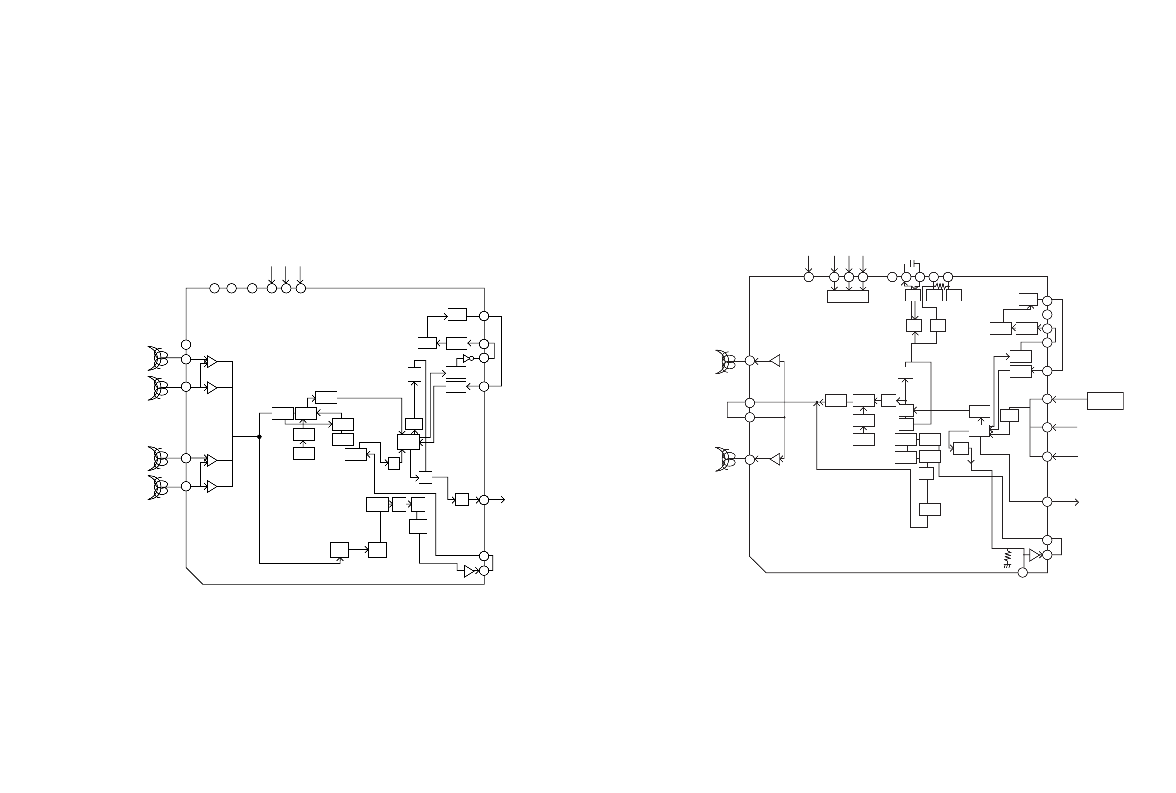
1. POWER(SMPS) BLOCK DIAGRAM 1
BD101
LINE FILTER
BLOCK
( C101, C102,
L101, L102 )
!
V101
!
F101
BD101
C103
DRIVE & S/W BLOCK
QUASI-RESONANT BLOCK
( IC101, R114, R115, C123, C107,
BC101, D108, R101, D102, R102,
D103, R106, ZD102, Z101, C108,
R104, C109, C110)
DRIVE & S/W BLOCK
SOFT-START BLOCK
( R107, R108, C121, R105,
C120, C119, ZD1103, D105,
R111, BC102 )
SNUBBER
BLOCK
( R110, C115,
D104, C117 )
!
!
IC102
!
T101
IC103
T102
RECTIFER & SMOOTHING
BLOCK
( D122, C131, R131,
C132, C133, C135, L122 )
FEED-BACK
BLOCK
( R122, R121, C136,
R123, R124, R125,
R126 )
RECTIFIER &
F102
SMOOTHING
BLOCK
(D123, C130, ZD121, R127)
RECTIFIER &
SMOOTHING
BLOCK
( D125, R129, C138 )
RECTIFIER & SMOOTHING
BLOCK
( D127, C142, L123, C146 )
RECTIFIER & SMOOTHING
BLOCK
( D124, C137, R128 )
RECTIFIER & SMOOTHING
BLOCK
( D126, C140, L122, C141 )
PSW01
32VA
NC
NC
PWR SENSE
PWR SENSE
BLOCK
( R184, R185 )
PSV01
FD(+)
FD(-)
-29VA
33VA
13VA
3.8VA
5.3VA
PW101
!
BR
BL
(BK)
(WH)
NOTES) Symbol denotes AC ground.
NOTES) Symbol denotes DC chassis ground.
C113C114
!!
C122
RECTIFIER & SMOOTHING
BLOCK
( D129, C144, L124, C147 )
FEED-BACK
BLOCK
!
!
IC105
IC106
( R132, R133, C148,
R134, R135, R136,
R137 )
TOSHIBA
SD-V55HTSU/SC
3-20 3-21
2. POWER(SMPS) BLOCK DIAGRAM 2
33VT BLOCK
(Q163, R168,
R169, R170)
TO SYS
FD(+)
TO SYS
FD(-)
TO SYS
-29VA
3.3V BLOCK
(IC161, C164)
TO TU
33V
FD(+)
FD(-)
-29VA
GND
33VA
GND
13VA
GND
3.8VA
3.8VA
GND
5.3VA
5.3VA
GND
GND
PVS01
15
14
13
12
11
10
1
2
3
4
5
6
7
8
9
10
11
12
TO SYS
PVD01
5.3VA
5.0V
8V
GND (M)
9V
GND (A)
3.3V
5V
GND
3.5V
A.GND
D.GND
5.3VA
8V BLOCK
(IC160, D163,
C163, R161)
9V BLOCK
(Q162, R171, ZD163)
9
8
7
6
5
4
3
2
3.3V BLOCK
(IC163, C177)
3.5V BLOCK
(IC162, D165, C172)
5V BLOCK
(Q168, R178, R179,
R180, C169)
5.2V BLOCK
(Q167, C168, R175,
R176, R177)
1
TO TU/SYS/ Hi-Fi
5.2V
FROM µ-COM
PWR CTL 'H'
TO AVCP
REG 5V
REG 5V
(Q166, C166, C167,
R174, ZD161)
PWR CTL BLOCK
(Q169, C170, R181,
R182, R183)
TOSHIBA
SD-V55HTSU/SC
3-22 3-23
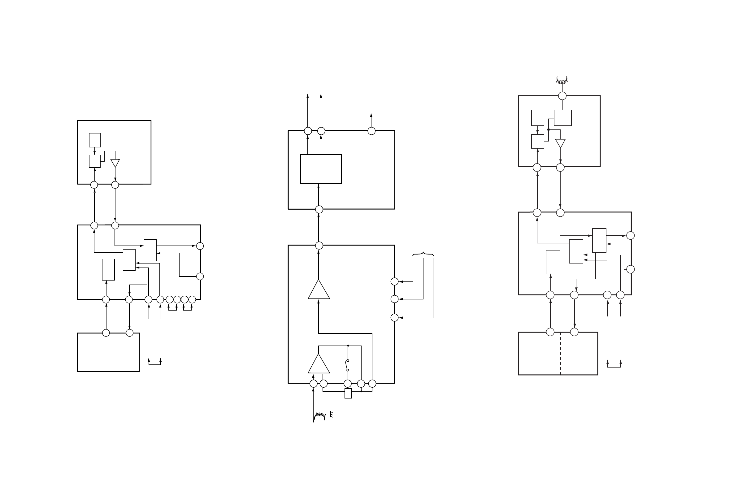
3. Y/C BLOCK DIAGRAM
EP PB 'A'
EP PB 'B'
SP PB 'B'
SP PB 'A'
64
59 58 57 55 54 53
65
67
72
74
ACC
DET
ENV
DET
C-ROT
RF-SW
IN
Y/C ENA
Y/C DATA
Y/C CLOCK
V.OUT
AUDIO
MUTE
HA SW
P
P
P
C-LPF
MAIN
CONV
3.58M
BPF2
ACC
AMP
ACC
DET
CLAMP
Y
LPF
CLAMP
CLAMP
IN
OUT
VCA
CCD
3.58M
BPF1
Y/C
MIX
6dB
DOUBLE
LIMFMDEM
SUB
LPF
MAIN
DE-EM
PB
FM-EQ
FM
AGC
CNC
YNR
COMB
4.21M
BPF
SUB
CONV
39
37
36
34
26
22
21
P
B
(PB Mode)
(REC Mode)
V. H/SW55Y/C ENA
57
Y/C DATA
Y/C CLOCK
54
53 51 50 49 48 47
SERIAL
DECODER
X-TAL
3.58MHZ
320FH
VCO
SLDVX01
OUT
39
38
REC
REC
APC
AFC
R
SP REC
EP REC
66
BGA
MAIN
CONV
4.21M
BPF
SUB
CONV
B-UP
AMP
ACC
AMP
ACC
DET
DETAIL
ENH
NL
EMPHA
CLAMP
MAIN
EMPHA
FM
MOD
REC
FM-EQ
LPF
3.58M
BPF1
YNR
COMB
Y
69
C-LPF
70
R
73
CCD
VIDEO
4.7K
AGC
CLAMP
VCA
CLAMP
20
37
IN
36
34
TU/LINE1
32
DVD
30
LINE2
28
V.OUT
26
IC302
SW
BLOCK
22
21
B
TOSHIBA
SD-V55HTSU/SC
3-24 3-25
4. NORMAL AUDIO BLOCK DIAGRAM
IC301
LA71206M
SIF
A_IN
RF_MOD
IC801
LA72670M
TUNER
TU701
10
76
DET
NORMAL
AUDIO
OUT
LINE AUDIO(R) IN
LINE AUDIO(L) IN
REAR JACK
REAR Jack
A. OUT (L)
ALC
SIF
DE MOD
INPUT
SELECT
OUTPUT
SELECT
4
6
13
1
57
9
2
71
117312
74
80
78
A. OUT (R)
DVD AUDIO
(System)
IC801
LA72670M
IC301
LA71206M
AMP
EQ
AMP
78
410
A. OUT (R)
MOD. OUT
DATA
CLOCK
R/P HEAD
N.A.IN
53
ENA
55 54
5
4
6
From u-COM
80
A. OUT (L)
2
OUTPUT
SELECTOR
EQ
3
2
1) EE Mode 2) PB Mode 3) REC Mode
9
IC301
LA71206M
IC801
LA72670M
TU701
TUNER
DET
ALC
76
NORMAL
AUDIO
OUT
6
SIF
DE MOD
13 57
SIF
REC
AMP
10
4
RF MOD.
INPUT
SELECT
1 2
A_IN
OUTPUT
SELECT
9
71
LINE AUDIO(L) IN
LINE AUDIO(R) IN
REAR Jack
78
A. OUT (R)
80
A. OUT (L)
TOSHIBA
SD-V55HTSU/SC
 Loading...