

TOSHIBA SD-5915SU, SD-5915SC Service Manual

SERVICE MANUAL
DIGITAL VIDEO
DVD VIDEO PLAYER
FILE NO. 813-9907
SD-5109
– SUMMARY –
This service manual covers only the different points from the service manual, file no. 810-9903,
for model SD-3109 since SD-5109 is basically the same designing as SD-3109.
Please refer to the file no. 810-9903 for other information.
Mar., 2000 s
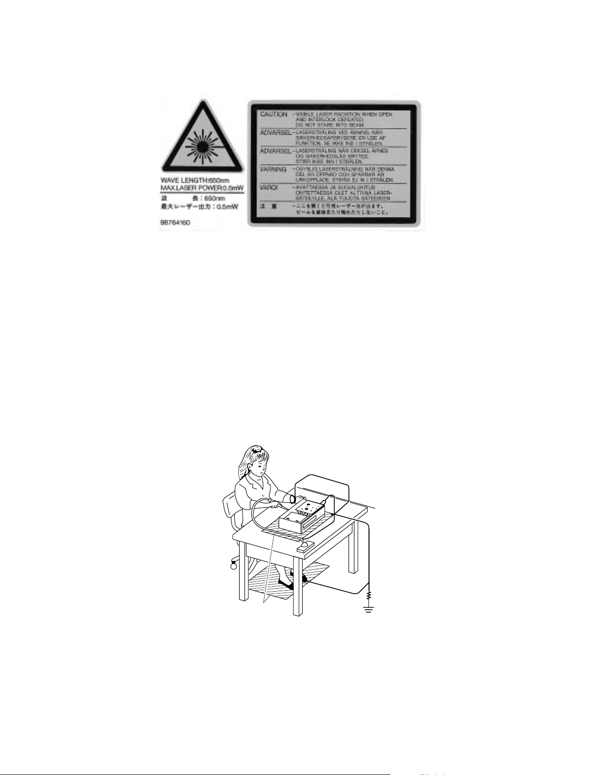
LASER BEAM CAUTION LABEL
When the power supply is being turned on, you may not remove this laser cautions label. If it removes, radiation of a laser
may be recceived.
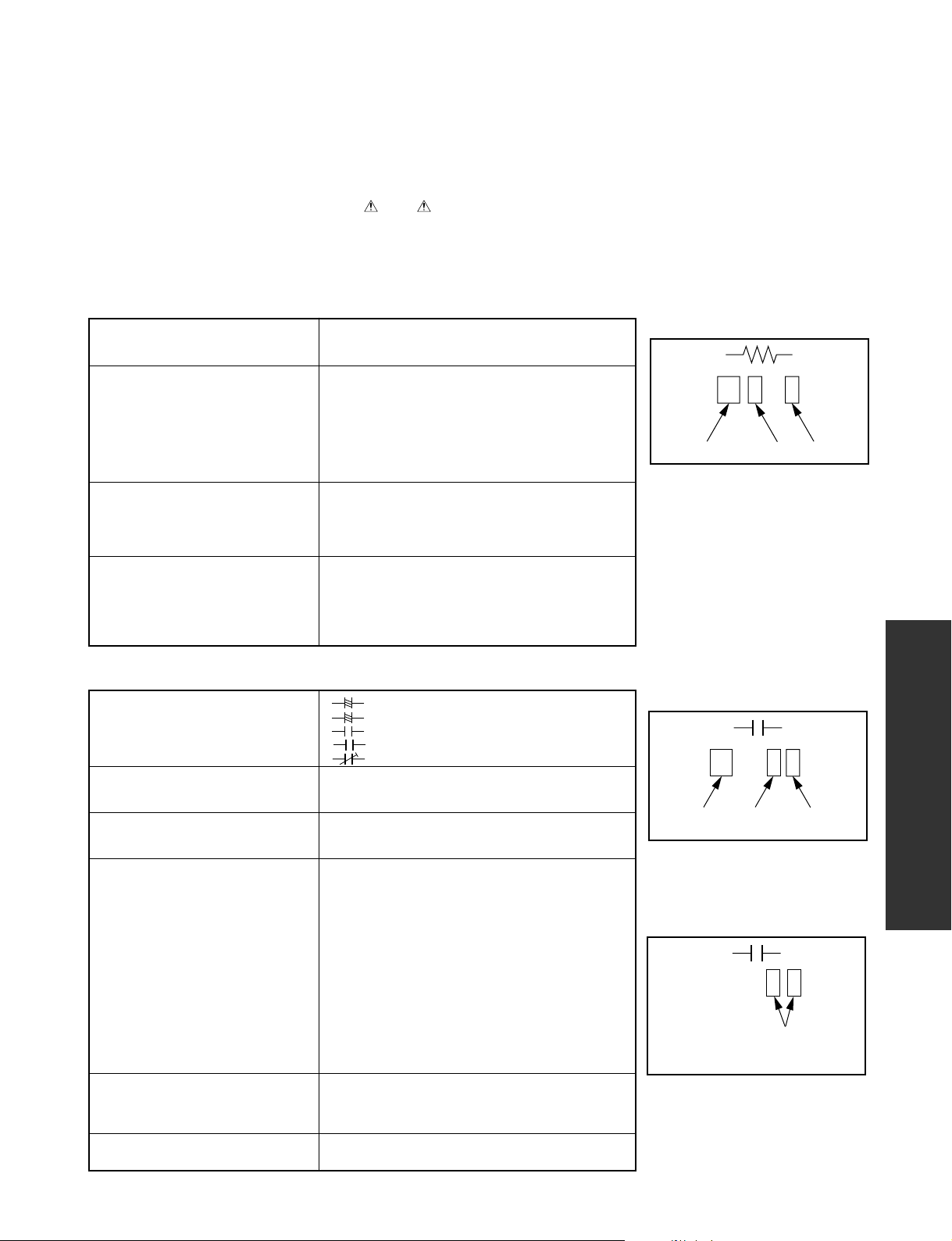
PREPARATION OF SERVICING
Pickup Head consists of a laser diode that is very susceptible to external static electricity.
Although it operates properly after replacement, if it was subject to electrostatic discharge during replacement, its
life might be shortened. When replacing, use a conductive mat, soldering iron with ground wire, etc. to protect the
laser diode from damage by static electricity.
And also, the LSI and IC are same as above.
Ground conductive
wrist strap for body.
Soldering iron
with ground wire
or ceramic type
1MΩ
Conductive mat
The ground resistance
between the ground line
and the ground is less than 10Ω.

GENERAL DESCRIPTIONS
CONTENTS
SECTION 1
GENERAL DESCRIPTIONS
1.OPERATING INSTRUCTIONS
General descriptions such as location of mechanical parts and troubleshooting are the same as SD-3109.
Please refer to the service manual for SD-3109 (File No. 810-9903).
SECTION 2
PART REPLACEMENT AND ADJUSTMENT PROCEDURES
Part replacement and adjustment procedures are the same as SD-3109.
Please refer to the service manual for SD-3109 (File No. 810-9903).
SECTION1
SERVICING DIAGRAMS
1.CIRCUIT SYMBOLS AND
SUPPLEMENTARY EXPLANATION
1-1.Precautions for Part Replacement
1-2.Solid Resistor Indication
1-3.Capacitance Indication
1-4.Inductor Indication
1-5.Waveform and Voltage Measurement
1-6.Others
1-7.When Replaced ROM ICs or Upgraded Firmware
2.PRINTED WIRING BOARD ANDSCHEMATIC DIAGRAM
SAFETY PRECAUTION
NOTICE
ABBREVIATIONS
1. Integrated Circuit (IC)
2. Capacitor (Cap)
3. Resistor (Res)
SECTION 3
3.BLOCK DIAGRAMS
3-1.Overall Block Diagram
3-2.Front Display, Power Switch Block Diagram
3-3.Main Block Diagram
3-3-1.Logical System Block Diagram
3-4.Output Block Diagram
4.CIRCUIT DIAGRAMS
4-1.Front Display, Power Switch Circuit Diagram
4-2.Output Circuit Diagram
4-2.Sub Video Circuit Diagram
SECTION 4
PARTS LIST
4.EXPLODED VIEWS
4-1.Packing Assembly
4-2.Chassis Assembly
4-3.Mechanism Assembly
5.PARTS LIST
SECTION 3
100k
Rated Wattage Type Tolerance
100µ
Temperature
response
Rated
voltage
Tolerance
SERVICING DIAGRAMS
1. CIRCUIT SYMBOLS AND SUPPLEMENTARY EXPLANATION
1-1. Precautions for Part Replacement
• In the schematic diagram, parts marked (ex.
F801) are critical part to meet the safety regulations,
so always use the parts bearing specified part codes
(SN) when replacing them.
1-2. Solid Resistor Indication
Unit None ...........W
K ...........kW
M ...........MW
Tolerance None ...........±5%
B ...........±0.1%
C ...........±0.25%
D ...........±0.5%
F ...........±1%
G ...........±2%
K ...........±10%
M ...........±20%
Rated Wattage (1) Chip Parts
None.........1/16W
(2) Other Parts
None.........1/6W
Other than above, described in the Circuit Diagram.
Type None ...........Carbon film
S ...........Solid
R ...........Oxide metal film
W ...........Metal film
W ...........Cement
FR ...........Fusible
• Using the parts other than those specified shall violate
the regulations, and may cause troubles such as
operation failures, fire etc.
Eg. 1
Fig. 3-1-1
1-3. Capacitance Indication
Symbol
Unit None ...........F
Rated voltage None ...........50V
Tolerance (1) Ceramic, plastic, and film capacitors of which
Temperature characteristic None ........... SL
(Ceramic capacitor) For others, temperature characteristics are
Static electricity capacity Sometimes described with abbreviated letters as
(Ceramic capacitor) shown in Eg. 3.
+
........... Electrolytic, Special electrolytic
NP
...........Non polarity electrolytic
...........Ceramic, plastic
M
...........Film
...........Trimmer
m ...........mF
p ...........p F
For other than 50V and electrolytic capacitors,
described in the Circuit Diagram.
capacitance are more than 10 pF.
None ...........±5% or more
B ...........±0.1%
C ...........±0.25%
D ...........±0.5%
F ...........±1%
G ...........±2%
(2) Ceramic, plastic, and film capacitors of which
capacitance are 10 pF or less.
None ...........more than ±5% pF
B ...........±0.1 pF
C ...........±0.25 pF
(3) Electrolytic, Trimmer
Tolerance is not described.
described. (For capacitors of 0.01 mF and
no indications are described as F.)
Eg. 2
Fig. 3-1-2
Eg. 3
104
4
pF (0.1µF)
10x10
Temperature characteristic
(or Temperature characteristic+
Static electricity capacity tolerance)
Fig. 3-1-3
SERVICING DIAGRAMS
SECTION 3
1-4. Inductor Indication
Type name
10µ
Type Tolerance
Unit None ...........H
m ...........mH
m ...........mH
Tolerance None ...........±5%
B ...........±0.1%
C ...........±0.25%
D ...........±0.5%
F ...........±1%
G ...........±2%
K ...........±10%
M ...........±20%
1-5. Waveform and Voltag e Measurement
• The waveforms for CD/DVD and RF shown in the
circuit diagrams are obtained when a test disc is
played back.
• All voltage values except the waveforms are expressed
in DC and measured by a digital voltmeter.
1-6. Others
• The parts marked with “NC” or “KETU” in the circuit
diagrams are not used for this model.
1-7. When Replaced ROM ICs or Upgraded Firmware
Eg. 4
Fig. 3-1-4
Eg. 5
Fig. 3-1-5
1. When replaced the following ROM ICs, it is necessary
to write the data into the new ICs.
1) IC615 (firmware)
2) IC613 (Setup default data and other information)
2. When the firmware is upgraded, rewriting the new
firmware into IC615 may be requested for servicing.
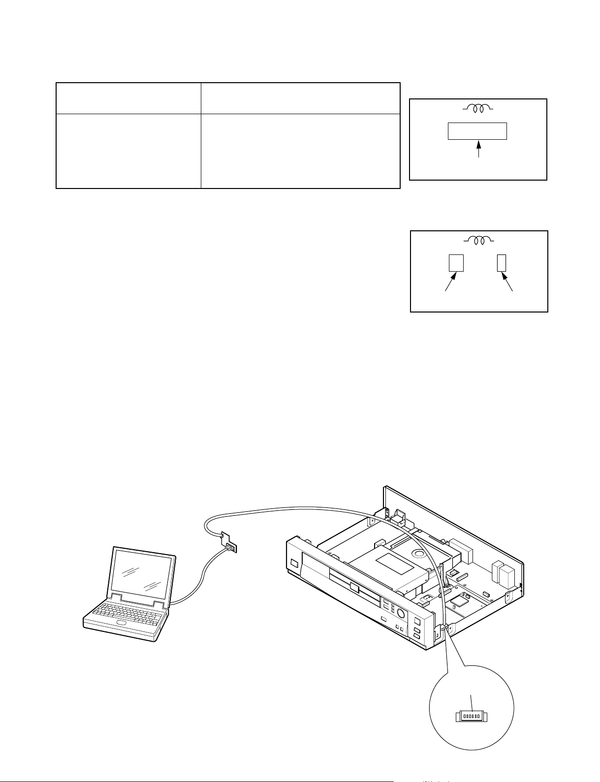
DATA UPDATE KIT
(RS232C Interface/cable)
RS-232C
cable
Computer
(MS-DOS/PC-DOS)
3. Connect a computer to the main PC board of the DVD
video player with using DATA UPDATE KIT (P/No.
79080074). (Fig. 3-2-6)
4. Writing operation
Refer to the instruction attached to the data floppy
disc.
Note:
• The firmware and setup data floppy discs are not available as service parts.
For more information, consult TOSHIBA service office in your area.
Fig. 3-1-6
CN601
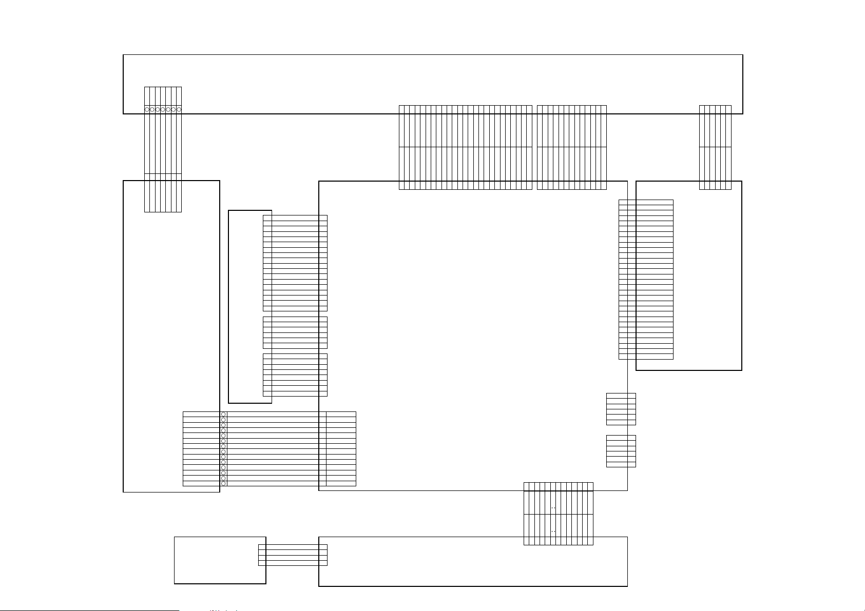
2. PRINTED WIRING BOARD AND SCHEMATIC DIAGRAM
EU05 OUTPUT
CNY02
Board-in
VEE-9V
E+6V
GND
NC
NON REG+6V
GND
-5V
-9V
CN802
EU02
POWER
CN801
Board-in
VCC+5V
GND
7654321
7P
Press-fit
7654321
ANALOG 5V
GND
E12V
EVER 5V
PO ON-OFF SIG
ANALOG 5V
NON REG +6V
ON-OFF 8V
DIGITAL 5V
DIGITAL 3V
GND
GND
GND
-24V
F2 (-)
F1 (+)
EU04 POWER-SW
MECHA
PUH
TRY
MOTOR
1
2
3
4
5
6
7
8
9
10
11
12
13
14
CN103 CN102
W501
FFC 1mm 18P
18
17
16
15
14
13
12
11
10
9
8
7
6
5
4
3
2
1
FFC 1.25mm 6P W502
6
5
4
3
2
1
FFC 1mm 8P W503
8
7
6
5
4
3
2
1
14P
Press-fit
FFC 1mm 4P
W102
GND
1
E+5V
2
POWLED
3
POWKEY
4
GND
VREF
VCC
FO
EO
AO
DO
CO
BO
F+
T T+
F VCC
GND
LD
MON
VOR
GND
LDMP
TOPN
LDMN
TCLS
TRAY
FMN
FMP
GND
LMT
DMN
DMP
VCC
DMFG
1
2
3
4
5
6
7
8
9
CN501
10
11
12
13
14
15
16
17
18
1
2
3
CN502
4
5
6
1
2
3
4
CN503
5
6
7
8
1
2
3
4
5
6
7
8
9
10
11
12
13
14
1
2
3
4
VCC+9V
ON-OFF 9V
DC+12V
E+5V
PWON
VCC+5V
VCC+6V
M+8V
VDD+5V
VDD+3V
GND
GND
MGND
VKK-24V
FF+
FFC 1mm 25P
W901
CN801
25
IEC958IN
Lch-IN
AGND
AGND
IEC958OUT
Lch-OUT
AGND
AGND
BIAS+5V
HMUTE
Rch-IN
Rch-OUT
BIAS+5V
HMUTE
CNY01 CNX01
101112131415161718192021222324
MIC-DATA
MIC-DATA
ZEROX
G+6dB
4448X
2131X
RSTX
X2fs
ZEROX
G+6dB
4448X
2131X
RSTX
X2fs
10
987654321
CN901 CN301
MIC ON
MCK
MIC ON
MCK
LRCK
LRCK
BCK
BCK
ADATA1
ADATA3
SDATA
SCLK
ADATA1
ADATA3
SDATA
SCLK
EU01 MAIN
FFC 1mm 13P
W301
EU03 FRONT
CNX02
101112
13
123456789
DA3CSX
DA2CSX
GND
DA3CSX
DA2CSX
GND
Y-INPUT
NTPALX
DGND
VGND
NC
NC
S1
Y-OUTPUT
NTPALX
DGND
VGND
NC
NC
S1
252423222120191817161514131211
CN603
987654321
DSPCKX
DSPRST
DSPSO
DSTBX
STBYX
DSPSI
E+5V
GND
GND
DSPCKX
DSPRST
DSPSO
DSTBX
STBYX
DSPSI
E+5V
GND
GND
101112
13
CN101
C
B-INPUT
VGND
C
B-OUTPUT
VGND
987654321
10
VKK-34V
GND
VKK-34V
GND
C-INPUT
VGND
C-OUTPUT
VGND
10
CN602
CN601
131211
F+
F-
F+
F-
123456789
123456789
CR-INPUT
VGND
FFC 1mm 13P
C
R-OUTPUT
VGND
131211
GND
TXD
CTS
RXD
RTS
GND
TXD
CTS
RXD
RTS
5V
5V
W301
1
2
3
4
5
6
7
8
9
10
11
12
13
14
15
16
17
18
19
20
21
22
23
24
25
26
27
28
29
30
10
11
12
13
14
15
16
17
18
19
20
21
22
23
24
25
26
27
28
29
30
1
2
3
4
5
6
7
8
9
1
2
3
4
5
6
1
2
3
4
5
6
CNV01CN302
GND
GND
VDD3.3V
VDD3.3V
VSYNC0
HSYNC0
BLANK0
RGBSX
CVSX
PCLP
S1
12C-CLK
12C-DATA
27MHz
R656-7
R656-6
R656-5
R656-4
R656-3
R656-2
R656-1
R656-0
FI 0
FI 1
RSTX
VCC+5V
VCC+5V
GND
GND
GND
FFC 1mm 6P
WV02
EU16 SUB VIDEO
6
I/P-V GND
I/P-CB
I/P-Y
PB-OUTPUT
YP-OUTPUT
GND
1
CNV02
I/P-V GND
I/P-CR
RP-OUTPUT
GND
12345
I/P-V GND
GND
65432
Fig. 3-2-1
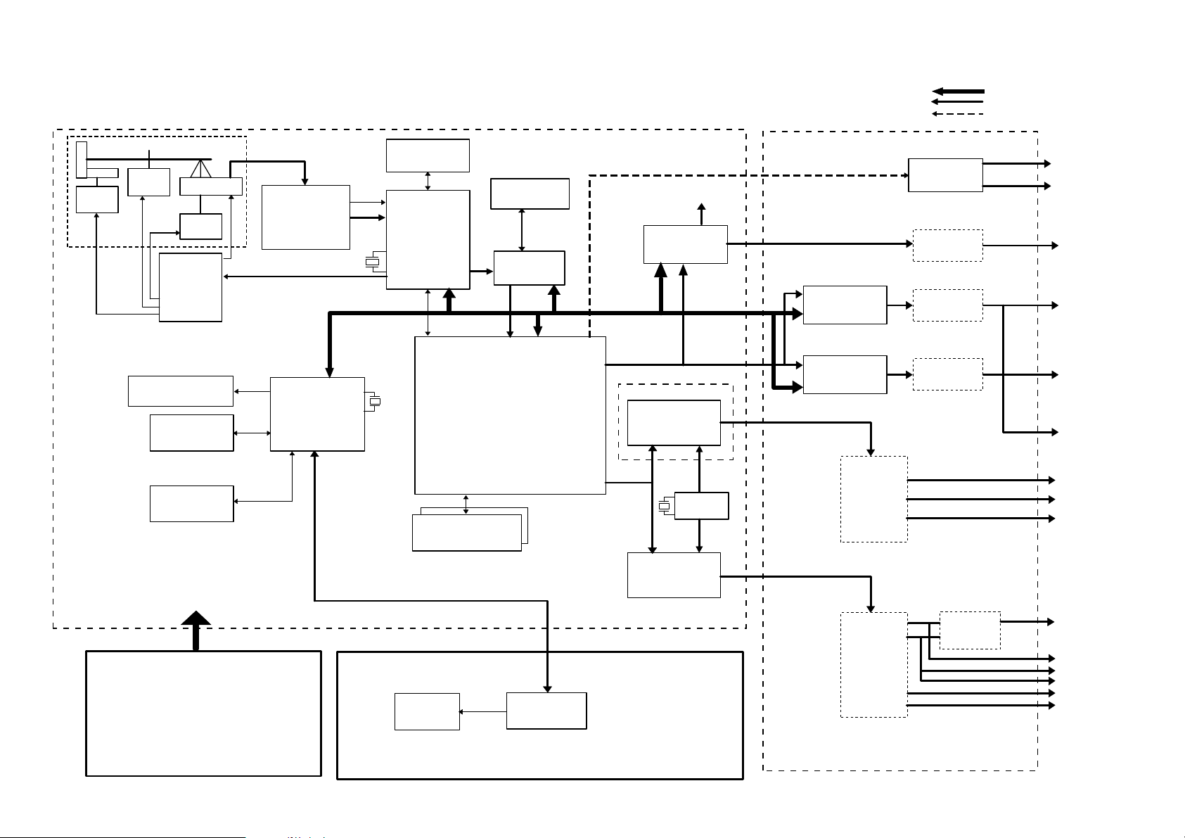
3. BLOCK DIAGRAMS
3-1. Overall Block Diagram
Data/Control Bus
DVD AV Data
SP DIF Data
Tray
Motor
SPM
Feed
Motor
PUH Driver
Motor Driver
IC504
KA3032
IC615
MBM29F800TA-55
8M-FROM
EE-PROM
IC613
S24C04BFJ-TB
2M-DRAM
IC614
HY512264JC-50
PUH
RF Amp.
IC501
TA1293F
IC601
TMP94CS40AF
Main-CPU
IC503
HY512264JC-50
X501
22. 5792
MHz
IC502
TC9453F
MD36710X
X601
9MHz
CeraOSC
2M-DRAM
1chip-SERVO
Data Processor
IC301
Video Process,MPEG-2 Decoder
16M-S-DRAM
IC305,302
HY57V16160ALTC-10 x2
MAIN PROCESSOR UNIT AUDIO/VIDEO OUTPUT UNIT
IC202
MSM514800C-70
4M-DRAM
TC203G08AF
IC201
-0103(Z)
Track Buffer
Decryption,
Dolby-Digital Decoder, OSD
ZORAN
IC901
PCM1727
Audio-DAC
PCM1727
SUB VIDEO UNIT
ICV01 TC200E2650AF
I-P CONV
IC306
ADV7170
Video Encoder
384fs Audio
Master Clock
27MHz
Xtal OSC
ICY09
ICY01
AD71010 or AD1854
Audio-DAC1
ICY31
AD71010 or AD1854
Audio-DAC3
LPF & P.Video
Out x 3ch
Buffer
TC74HCU04AF
LPF&
Amplifier
Audio Out
LPF&
Amplifier
Audio Out
LPF&
Amplifier
Audio Out
Coaxial Digital
Audio Out
TOS Link Digital
Audio Out
SL,SR Analog
Audio Out
FL,FR Analog
Audio out
Center SW
Analog
Audio Out
FL2,FR2 Analog
Audio Out
Y, PB, PR
PROGRESSIVE
VIDEO OUT
SW POWER SUPPLY
Display
(FL)
Display-CPU
FRONT DISPLAY UNIT
IC101
TMP47C416F
LPF & Video
Out x 4ch
Y,C Mixer
&Buffer
Composite Video
Out
S Video Out
Y,C
B,CR
video
Interlaced Out
Fig.3-3-1
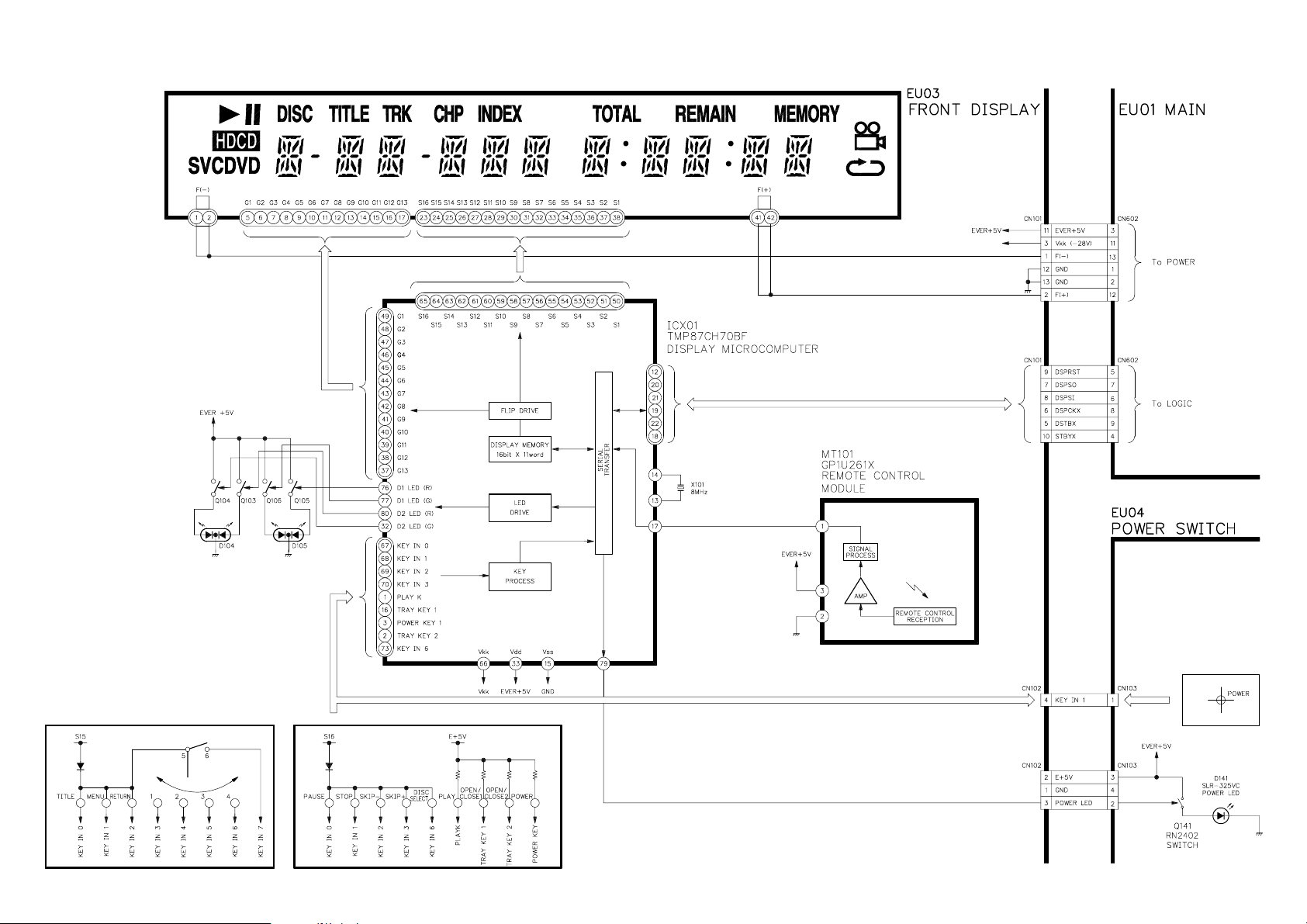
3-2. Front Display, Power Switch Block Diagram
Fig. 3-3-2
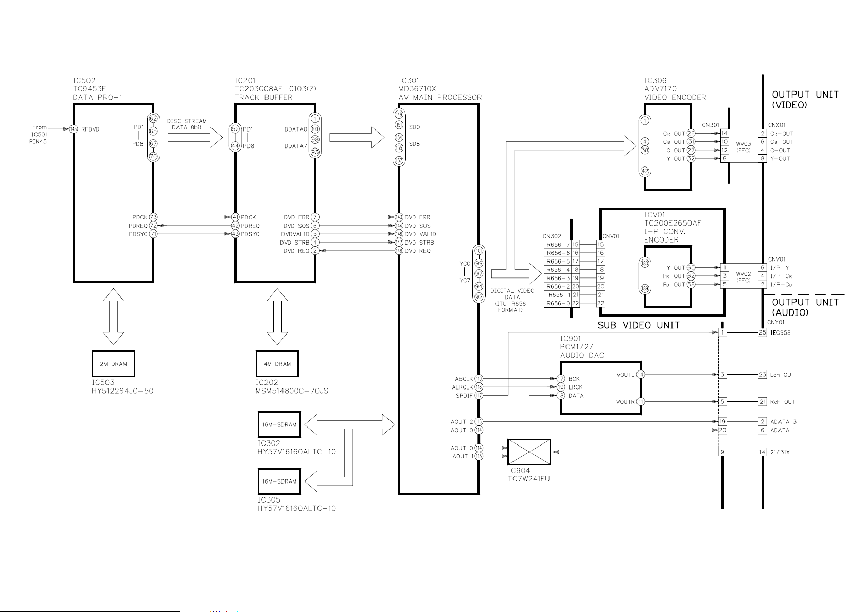
3-3. Main Block Diagrams
3-3-1. Logical System Block Diagram
Fig. 3-3-3
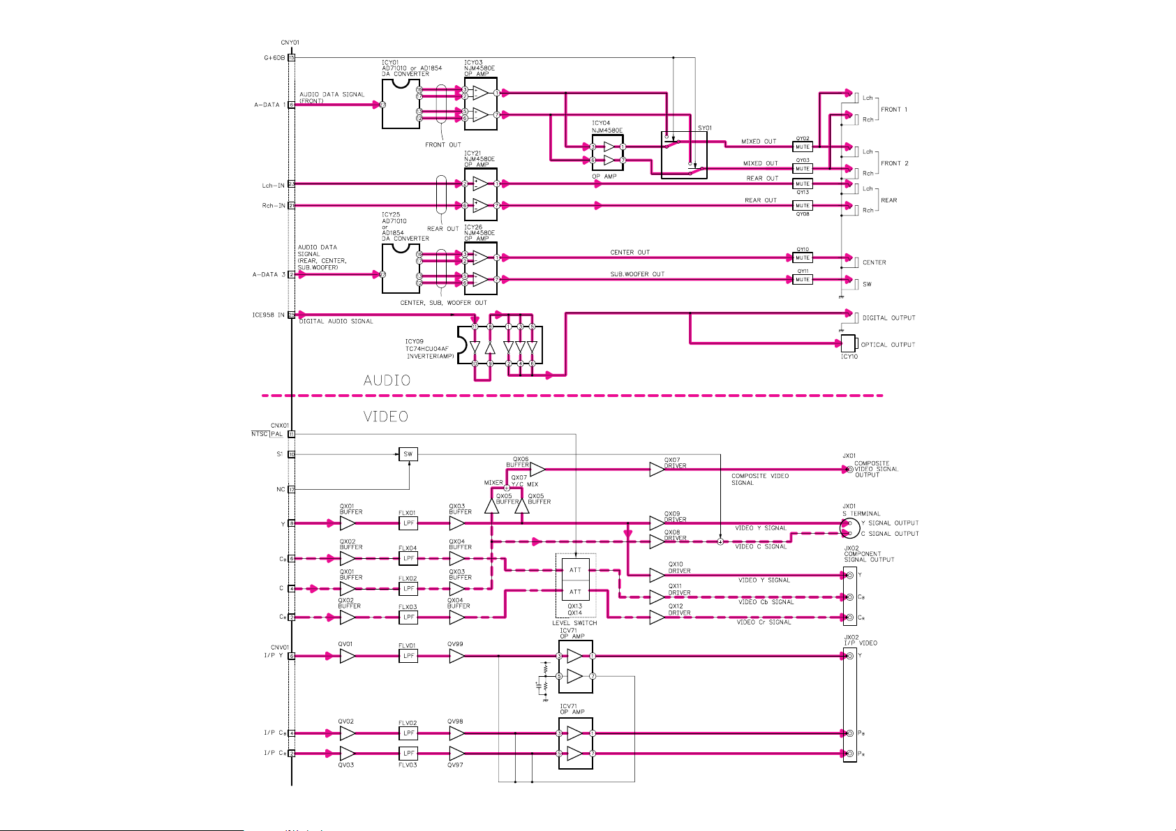
3-4. Output Block Diagram
Fig. 3-3-4
 Loading...