

Page 1

FILE NO. 060-200101
To CTV
SERVICE MANUAL
COLOUR TELEVISION
S9S Chassis
20N7XE
PRINTED IN JAPAN, Jan., 2001 T
Page 2

CHAPTER 1 GENERAL ADJUSTMENTS
SAFETY INSTRUCTIONS........................................................................................................................................3
SET-UP ADJUSTMENT ............................................................................................................................................ 4
SERVICE MODE ......................................................................................................................................................6
DESIGN MODE ........................................................................................................................................................9
ELECTRICAL ADJUSTMENT ................................................................................................................................ 10
CIRCUIT CHECK....................................................................................................................................................17
GENERAL ADJUSTMENTS
CHAPTER 2 SPECIFIC INFORMATIONS
SETTING & ADJUSTING DATA ..............................................................................................................................18
LOCATION OF CONTROLS ................................................................................................................................... 19
PROGRAMMING CHANNEL MEMORY................................................................................................................. 20
CIRCUIT BLOCK DIAGRAM ..................................................................................................................................21
CHASSIS AND CABINET REPLACEMENT PARTS LIST......................................................................................22
PC BOARDS BOTTOM VIEW.................................................................................................................................29
TERMINAL VIEW OF TRANSISTORS ................................................................................................................... 33
TABLE OF CONTENTS
SPECIFIC INFORMATIONS
SPECIFICA TIONS .................................................................................................................................................. 37
APPENDIX:
CIRCUIT DIAGRAMS
– 2 –
Page 3

CHAPTER 1 GENERAL ADJUSTMENTS
SAFETY INSTRUCTIONS
WARNING: BEFORE SERVICING THIS CHASSIS, READ THE “X-RAY RADIATION PRECAUTION”, “SAFETY PRECAU-
TION” AND “PRODUCT SAFETY NOTICE” INSTRUCTIONS BELOW.
X-RAY RADIATION PRECAUTION
1. Excessive high voltage can produce potentially hazardous X-RAY RADIATION. To avoid such hazards, the high
voltage must not be abov e the specified limit. The nominal
value of the high voltage of this receiver is (A)kV at zero
beam current (minimum brightness) under a (C)V AC power
source. The high voltage must not, under any circumstances, exceed (B)kV.
Refer to table-1 for high v oltage (A), (B) & A C v oltage (C)
(See SETTING & ADJUSTING DATA on page 18)
Each time a receiver requires servicing, the high voltage
should be checked f ollowing the HIGH VOLT AGE CHECK
procedure in this manual. It is recommended that the reading of the high voltage be recorded as a part of the service
record. It is important to use an accurate and reliable high
voltage meter.
SAFETY PRECAUTION
WARNING : Service should not be attempted by anyone unfamiliar with the necessary precautions on this receiver. The f ollowing are the necessary precautions to be observed before servicing this chassis.
1. An isolation transformer should be connected in the power line between the receiver and the AC line before any service is
performed on the receiver.
2. Always discharge the picture tube anode to the CR T conductive coating before handling the picture tube. The picture tube
is highly evacuated and if broken, glass fragments will be violently expelled. Use shatter proof goggles and keep picture
tube away from the unprotected body while handling.
3. When replacing a chassis in the cabinet, always be certain that all the protective devices are put back in place, such as; nonmetallic control knobs, insulating covers, shields, isolation resistor-capacitor network etc.
2. The only source of X-RAY RADIATION in this TV receiver
is the picture tube. F or contin ued X-RAY RADIATION protection, the replacement tube must be exactly the same
type tube as specified in the parts list.
3. Some part in this receiver have special safety-related characteristics for X-RAY RADIATION protection. For continued safety, parts replacement should be undertaken only
after referring to the PRODUCT SAFETY NO TICE below.
GENERAL ADJUSTMENTS
SPECIFIC INFORMATIONS
PRODUCT SAFETY NOTICE
Many electrical and mechanical parts in this chassis have special safety-related characteristics. These characteristics are
often passed unnoticed by a visual inspection and the protection afforded by them cannot necessarily be obtained b y using
replacement components rated for higher voltage, w attage, etc. Replacement parts which have these special saf ety characteristics are identified in this manual and its supplements; electrical components having such features are identified by the
international hazard symbols on the schematic diagram and the parts list.
Before replacing any of these components, read the parts list in this manual carefully. The use of substitute replacement
parts which do not have the same safety characteristics as specified in the parts list may create shock, fire, X-ray radiation
or other hazards.
– 3 –
Page 4
WARNING: BEFORE SERVICING THIS CHASSIS, READ THE “X-RAY RADIATION PRECAUTION”, “SAFETY PRECAUTION” AND “PRODUCT SAFETY NOTICE” ON PAGE 3 OF THIS MANUAL.
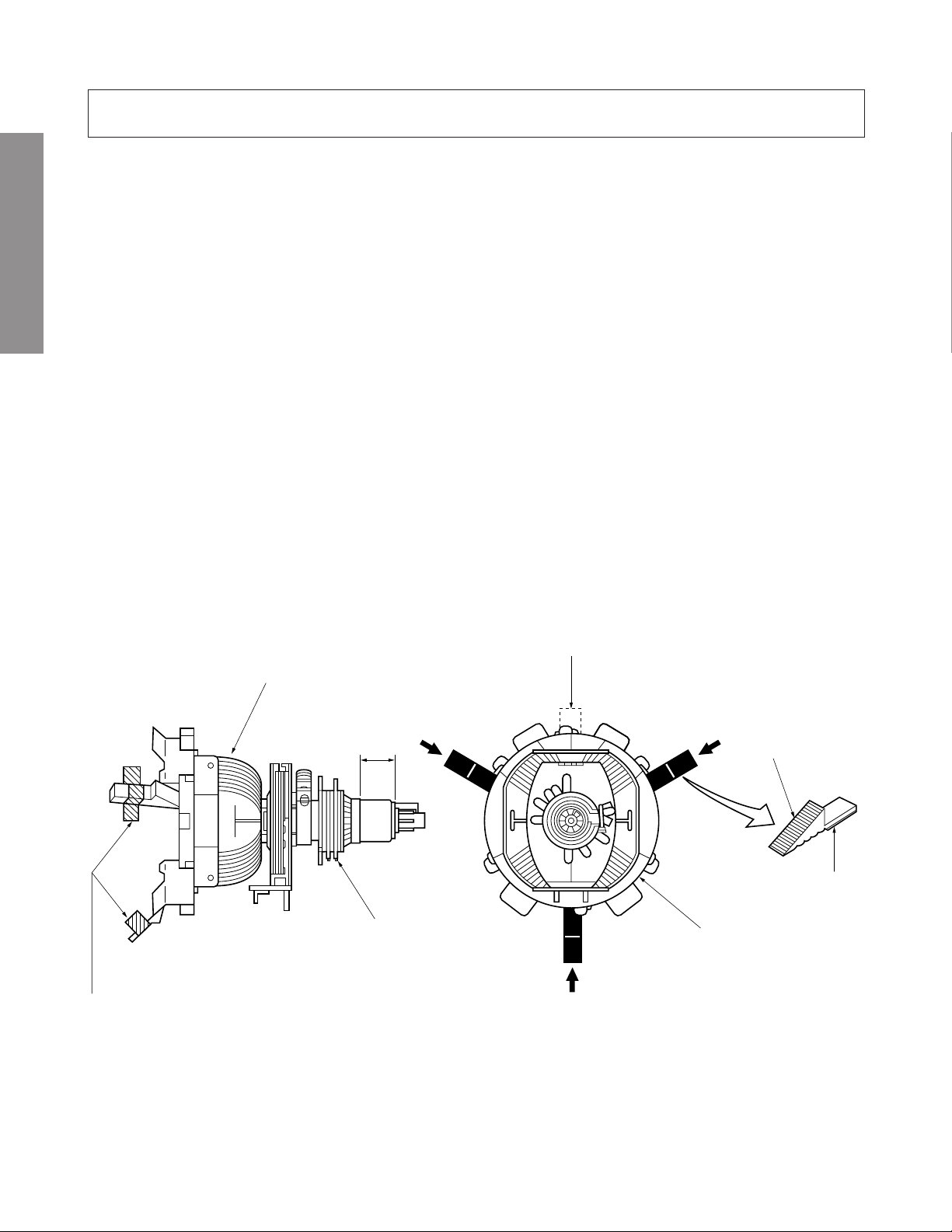
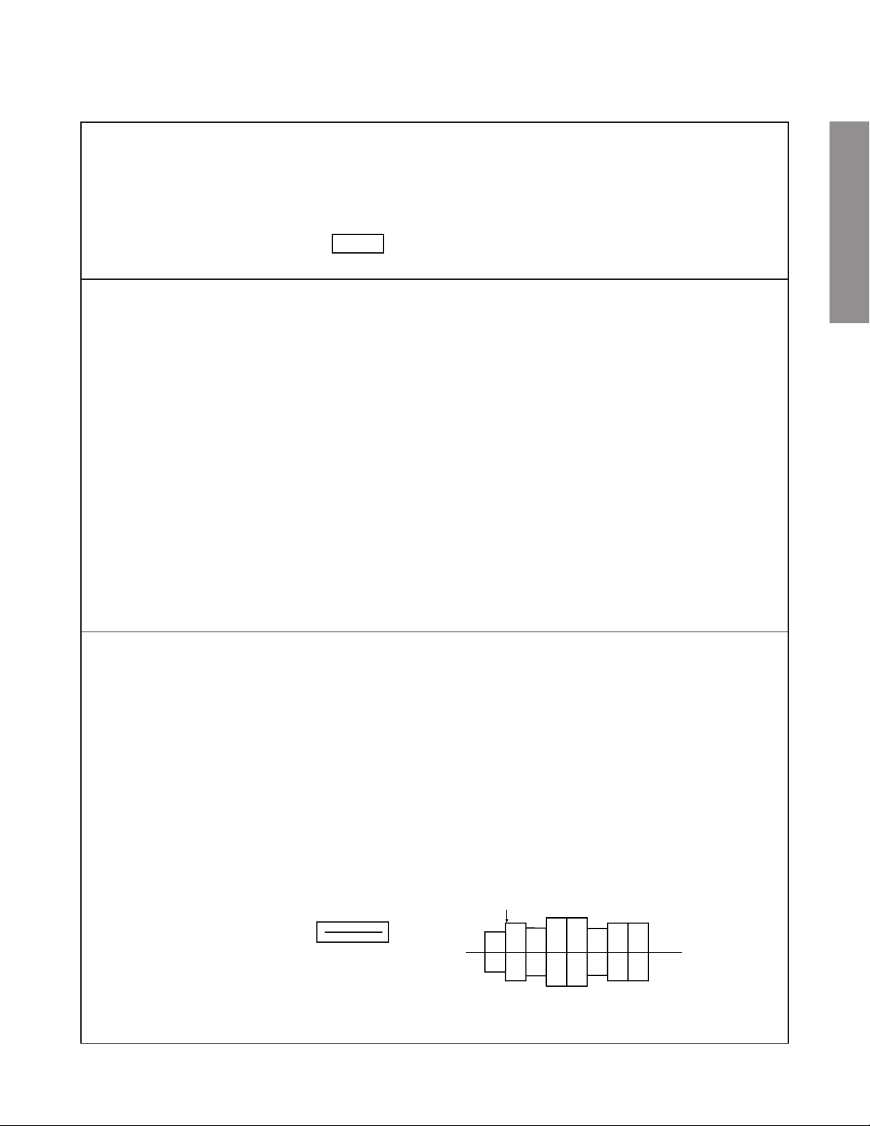
■ The following adjustments should be made when a complete realignment is required or a new picture tube is installed.
Perform the adjustments in order as follows :
1. Color Purity
2. Convergence
3. White Balance
Note: • The PURITY/CONVERGENCE MAGNET assembly and rubber wedges need mechanical positioning.
Refer to figure 1.
GENERAL ADJUSTMENTS
*
COLOR PURITY ADJUSTMENT
NOTE : Before attempting any purity adjustments, the receiver
1. Demagnetize the picture tube and cabinet using a degauss-
2. Set the brightness and contrast to maximum.
3. Use a green raster from among the built-in test signals.
4. Loosen the clamp screw holding the yoke and slide the
• Mounting position of the purity magnet assembly should fit to same position as old one because slightly difference
to the position depend on a tube.
There are no adjustment of purity and convergence in some picture tube (Unified with purity magnet)
should be operated for at least fifteen minutes.
ing coil.
yoke backward or forward to provide vertical green belt
(zone) in the picture screen.
SPECIFIC INFORMATIONS
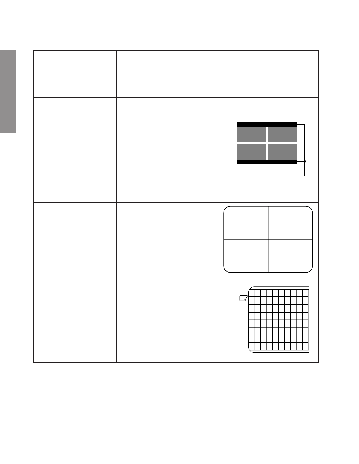
SET-UP ADJUSTMENT
5. Remove the Rubber Wedges.
6. Rotate and spread the tabs of the purity magnet (See figure 2.) around the neck of the picture tube until the green
belt is in the center of the screen. At the same time , enter
the raster vertically.
7. Slowly move the yoke forward or backward until a uniform
green screen is obtained. Tighten the clamp screw of the
yoke temporarily.
8. Check the purity of the red and blue raster.
GLASS CLOTH
TAPES
DEFLECTION
YOKE
29.1mm(28", 29")
25mm(25")
19mm(19", 20", 21")
14mm(13", 14")
PURITY/
CONVERGENCE
MAGNET ASS'Y
Figure 1.
TEMPORARY
MOUNTING
RUBBER WEDGE
ADHESIVE
DEFLECTION
YOKE
– 4 –
Page 5
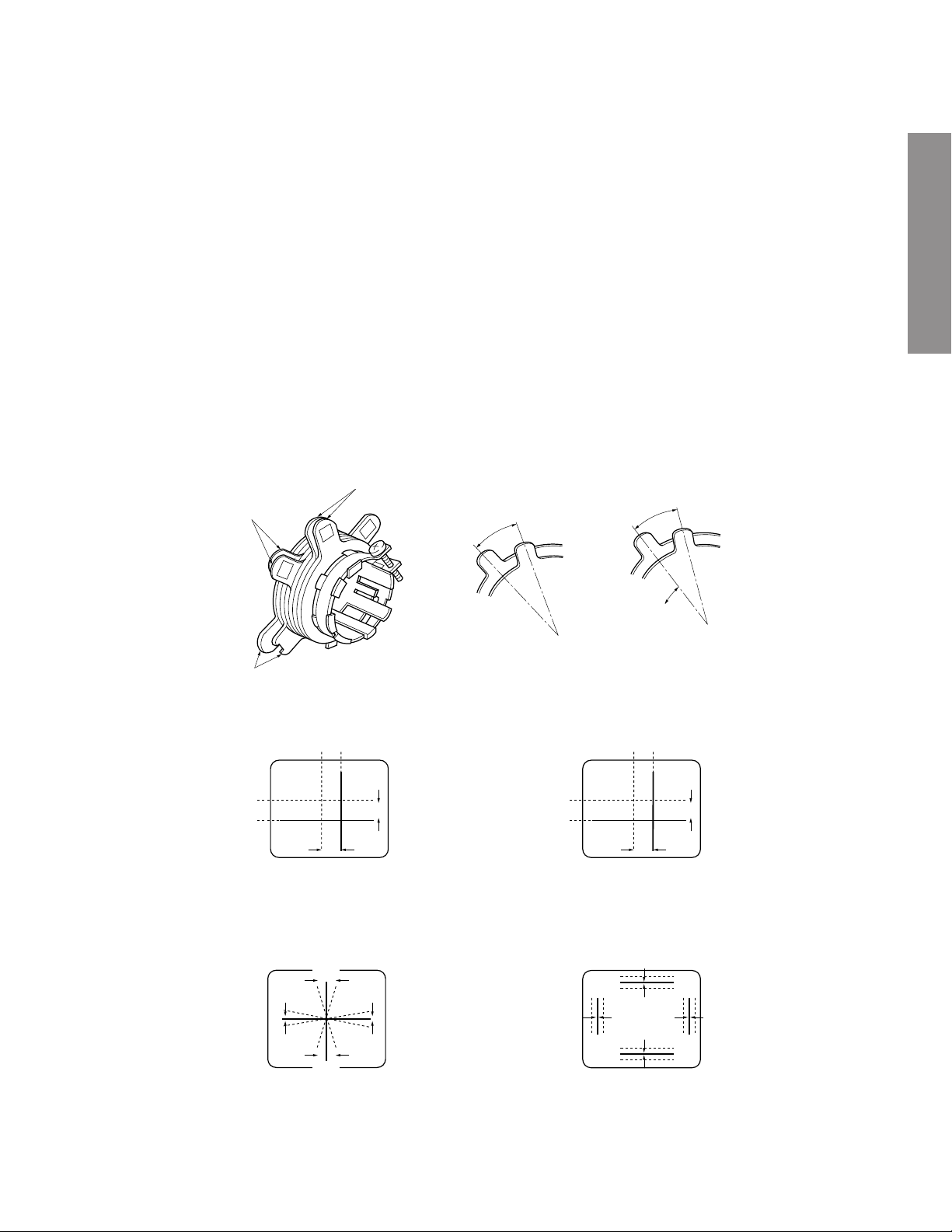
CONVERGENCE ADJUSTMENTS
NOTE: Before attempting any convergence adjustments, the
receiver should be operated for at least fifteen minutes.
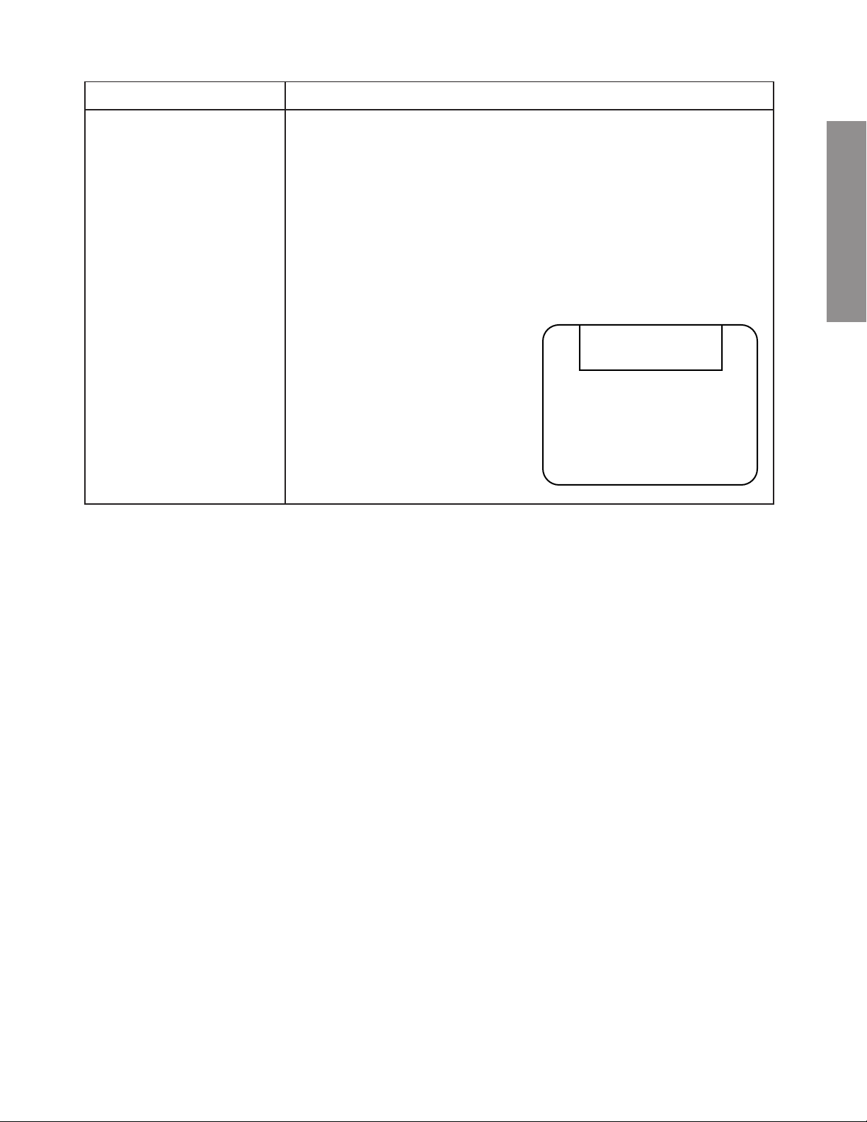
■ CENTER CONVERGENCE ADJUSTMENT
1. Use the cross-dot pattern from among the built-in test signals.
2. Set the brightness and contrast for well defined pattern.
3. Adjust two tabs of the 4-Pole Magnets to change the angle between them (See figure 2.) and superimpose red
and blue vertical lines in the center area of the picture
screen.
4. Turn the both tabs at the same time keeping the angle
constant to superimpose red and blue horizontal lines at
the center of the screen.
5. Adjust two tabs of 6-Pole Magnets to superimpose red/
blue line and green one. Adjusting the angle affects the
vertical lines and rotating both magnets affects the horizontal lines.
6. Repeat adjustments 3, 4, 5 keeping in mind red, green
and blue movement, because 4-Pole Magnets and 6-Pole
Magnets have mutual interaction and make dot movement
complex.
6-POLE
4-POLE
MAGNETS
MAGNETS
ADJUST THE ANGLE
(VERTICAL LINES)
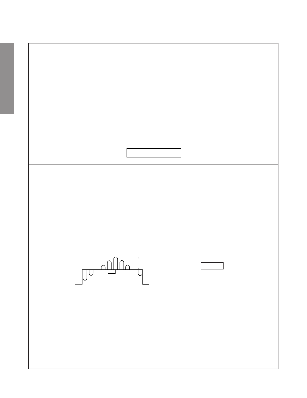
■ CIRCUMFERENCE CONVERGENCE ADJUSTMENT
1. Loosen the clamping screw of deflection yoke slightly to
allow the yoke to tilt.
2. Temporarily put a wedge as shown in figure 1. (Do not
remove cover paper on adhesive part of the wedge.)
3. Tilt front of the deflection yoke up or down to obtain better
convergence in circumference. (See figure 3.) Push the
mounted wedge into the space between picture tube and
the yoke to fix the yoke temporarily.
4. Put other wedge into bottom space and remove the cover
paper to stick.
5. Tilt front of the yoke right or left to obtain better convergence in circumference. (See figure 3.)
6. Keep the yoke position and put another wedge in either
upper space. Remove cover paper and stick the wedge
on picture tube to fix the yoke.
7. Detach the temporarily mounted wedge and put it in another upper space. Stick it on picture tube to fix the yoke.
8. After fixing three wedges, recheck overall convergence.
Tighten the screw firmly to fix the yoke and check the y oke
is firm.
9. Stick three adhesive tapes on wedges as shown in figure
1.
FIXED
GENERAL ADJUSTMENTS
ROTATE TWO TABS
AT THE SAME TIME
(HORIZONTAL LINES)
PURITY
MAGNETS
CONVERGENCE MAGNET ASSEMBLY ADJUSTMENT OF MAGNETS
Figure 2.
BLU RED
BLU
RED
4-POLE MAGNETS MOVEMENT
BGR
R
G
B
RGB
RED/BLU
GRN
Center Convergence by Convergence Magnets
B
G
R
RED/BLU GRN
6-POLE MAGNETS MOVEMENT
B
G
R
BGR
RGB
R
G
B
SPECIFIC INFORMATIONS
INCLINE THE YOKE UP (OR DOWN)
Circumference Convergence by DEF Yoke
Figure 3. Dot Movement Pattern
INCLINE THE YOKE RIGHT (OR LEFT)
– 5 –
Page 6
1. ENTERING TO SERVICE MODE
1) Press o button once on
Remote Control.
SERVICE MODE
2) Press o button again to
keep pressing.
3) While pressing the o button,
press MENU button on TV set.
GENERAL ADJUSTMENTS
2. DISPLAYING THE ADJUSTMENT MENU
1) Press MENU button on TV.
Adjustment mode
ITEM
DATA
3. KEY FUNCTION IN THE SERVICE MODE
The following key entry during display of adjustment menu provides special functions.
SPECIFIC INFORMATIONS
A single horizontal line ON/OFF: - / - - button (on Remote) or a button (on TV)
Test signal selection : a button (on Remote)
Selection of the adjustment items : CHANNEL s/t (on TV or Remote)
Change of the data value : VOLUME +/– (on TV or Remote)
Adjustment menu mode ON/OFF : MENU button on TV
Initialization of the memory (QA02) : CALL + CHANNEL button on TV (s)
Reset the count of operating protect
circuit to “00”: CALL + CHANNEL button on TV (t)
“RCUT” selection : 1 button
“GCUT” selection : 2 button
“BCUT” selection : 3 button
“CNTX” (or “SCNT”) selection : 4 button
“COLC” selection : 5 button
“TNTC” selection : 6 button
Test audio signal ON/OFF (1kHz) : 8 button
Self diagnostic display ON/OFF : 9 button
Item
Data
Press
Press
Item
Data
(Service mode display)
Service mode
S
S
Color thickness correction
note: Displayed differently as shown below, de-
pending on the setting of the receiving color
system.
COLP (PAL)
COLC (NTSC)
COLS (SECAM)
CAUTION : Never try to perform initialization unless you have changed the memory IC.
– 6 –
Page 7
4. SELECTING THE ADJUSTING ITEMS
1) Every pressing of CHANNEL s button in the service mode changes the adjustment items in the order of table-2.
(t button for reverse order)
Refer to table-2 for preset data of adjustment mode.
(See SETTING & ADJUSTING DATA on page 18)
5. ADJUSTING THE DATA
1) Pressing of VOLUME ; +/– button will change the value of data in the range from 00H to FFH. The variable
range depends on the adjusting item.
6. EXIT FROM SERVICE MODE
1) Pressing POWER button to turn off the TV once.
■ INITIALIZATION OF MEMORY DATA OF QA02
After replacing QA02, the following initialization is required.
1. Enter the service mode, then select any register item.
2. Press and hold the CALL button on the Remote, then press the CHANNEL s button on the TV. The initialization of QA02 has
been complated.
3. Check the picture carefully. If necessary, adjust any adjustment item above.
Perform “Auto search Memory” on the owner’s manual.
CAUTION: Never attempt to initialize the data unless QA02 has been replaced.
7. TEST SIGNAL SELECTION
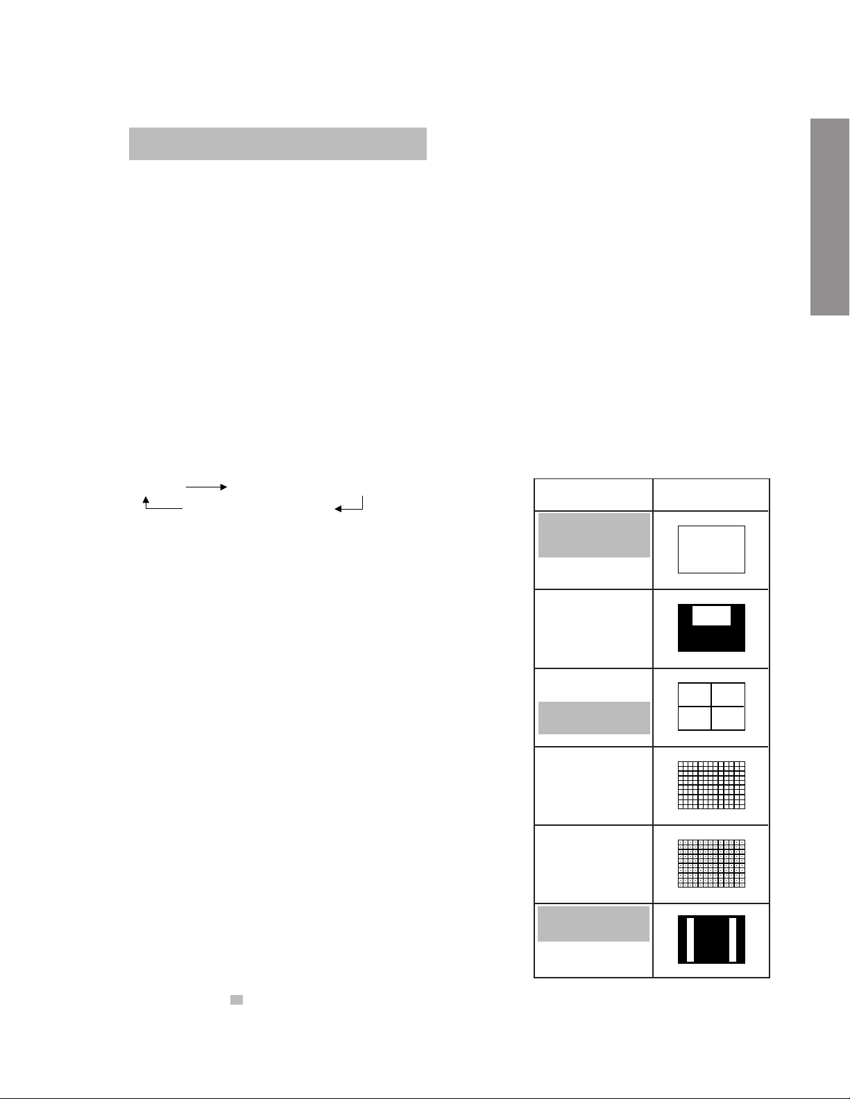
Every pressing of a button on the Remote Control changes the built-in test patterns on screen as described below in
SERVICE MODE.
GENERAL ADJUSTMENTS
Signal off
NTSC signals (14 patterns)
PAL signals (14 patterns)
Signals Picture
• Red raster
• Green raster
• Blue raster
• All Black
• All White
• Black & White
• Black cross-bar
• White cross-bar
• Black cross-bar
on green raster
• Black cross-hatch
• White cross-hatch
• Black cross-dot
• White cross-dot
SPECIFIC INFORMATIONS
• H signal (white)
• H signal (black)
The signals marked with are not usable to display in the Test signal for some model.
*
– 7 –
Page 8

8. SELF DIAGNOSTIC FUNCTION
1) Press “9” button on Remote Control during display of adjustment menu in the service mode.
The diagnosis will begin to check if interface among IC’s are executed properly.
2) During diagnosis, the following displays are shown.
<SELF CHECK>
23******
POWER : 00
BUS LINE : OK
BUS CONT : OK
BLOCK : UV V1 V2
(or SYNC) QV01 QV01S
GENERAL ADJUSTMENTS
Indicated color of mode now selected : Green and Red
Indicated color of other modes : White
Green :Normal
Red : The microcomputer operates to provide judgement
of no video signal. The red color is still indicated
though the signal is input, failure may exist in input
signal line including QV01.
QV01 : In case of indication green ---Normal
In case of indication red with input signal---Failure may exist in output line including QV01.
Part number of microcomputer (QA01)
Operation number of protecting circuit ----“00” is nor-
mal.
When indication is other than “00”, overcurrent apts to
flow, and circuit parts may possibly be damaged.
BUS LINE CHECK ----“OK” is normal.
“SCL(SCL1)-GND”...............SCL-GND short circuit
“SDA(SDA1)-GND” .............. SDA-GND short circuit
“SCL(SCL1)-SDA (SDA1)”... SCL-SDA short circuit
BUS CONT ----“OK” is normal.
When indication shows “Q uuu NG”, the device with
SPECIFIC INFORMATIONS
the number may possibly be damaged.
BLOCK ----“OK” is normal.
UV : TV reception mode
V1 : VIDEO 1 input mode (a1)
V2 : VIDEO 2 input mode (a2)
The items marked with are not usable to display in the SELF DIAGNOSTIC FUCTION for some model.
*
NOTE: Component which controls character display on
screen is QT01 (TELETEXT IC.). If this display
function fails to operate due to damage in QT01,
self diagnosis procedure is as follows.
(1) In case that power indicator is blinking with
interval of 0.5 seconds; it means protecting
circuit (Current limiter) is operating, and circuit components may possibly be damaged.
Check related components.
(2) In case that power indicator is blinking with
interval of 1 second; Protecting circuit does
not operate, but a part of Bus line does not
operate normally. Check Bus line.
– 8 –
Page 9

1. ENTERING TO DESIGN MODE
1) Select the Service mode.
DESIGN MODE
2) While pressing o (or CALL) button on
Remote and press MENU button on TV.
3) Press MENU button on TV.
S D
(Design mode) (Adjustment mode)
When QA02 is initialized, items “OPT0” and “OPT1” of DESIGN MODE are set to the data of the representative model of this
chassis family.
Therefore, because ON-SCREEN specification remains in the state of the representative of model. This model is required to
reset the data of items “OPT0” and “OPT1”.
2. SELECTING THE ADJUSTING ITEMS
Every pressing of CHANNEL t button in the design mode changes the adjustment items in the order of table-3.
Refer to table-3 for data of design mode.
(See SETTING & ADJUSTING DATA on page 18)
3. ADJUSTING THE DATA
Pressing of VOLUME s or t (; +/–) button will change the value of data.
Press
Press
ITEM
DATA
GENERAL ADJUSTMENTS
SPECIFIC INFORMATIONS
– 9 –
Page 10
ELECTRICAL ADJUSTMENT
ITEM ADJUSTMENT PROCEDURE
FOCUS VR ADJ.
SUB-BRIGHTNESS
(BRTC)
GENERAL ADJUSTMENTS
SPECIFIC INFORMATIONS
Note: Constrict the picture height
until the vertical retrace line
appears adjusting the item
HIT (HEIGHT).
HORIZONTAL POSITION
ADJUSTMENT (HPOS)
VERTICAL POSITION
ADJUSTMENT (VPOS)
1. Enter the service mode, then select any register item.
2. Press the TV/VIDEO button on the Remote until the black cross-bar pattern appears on the screen.
3. Adjust the FOCUS control (on T461) for well defined scanning lines on the picture
screen.
1. Set CONTRAST to minimum, and
BRIGHTNESS to center by adjusting user
controls.
2. Set the TV in service mode to get white
cross-bar of inside pattern.
3. Select BRTC (brightness correction), and
adjust the ; – /+ button to reduce the
value so that white portion of inside pattern slightly light.
4. Adjust ; – /+ button to increase the data
value of BRTC, and set it just before the
difference between the belt of vertical retrace and the border of black portion of
inside pattern is visible.
After that, return vertical height and contrast.
1. Set the TV in service mode, and get
black or white cross-bar signal with
VIDEO button on remote hand unit.
2. Select either HPOS (Hor izontal pic-
ture phase) or VPOS (V ertical picture
phase) with CHANNEL s, t buttons,
and adjust horizontal or vertical picture position in the center of screen
with VOLUME ; – /+ buttons.
Belt of vertical retrace
VERTICAL AMPLITUDE
ADJUSTMENT (HIT)
1. Set the TV in service mode, and get
black or white cross-hatch signal with
VIDEO button on remote hand unit.
2. Select HIT (Vertical amplitude) with
CHANNEL s, t buttons, and adjust
vertical amplitude with VOLUME
; – /+ buttons so that vertical amplitude lacks a little.
3. Adjust vertical amplitude with VOL-
UME ; – /+ buttons so that the first
bar on cross-hatch signal touches
edge of screen.
– 10 –
The first
Page 11
ITEM ADJUSTMENT PROCEDURE
WHITE BALANCE
ADJUSTMENT
CUTOFF ADJUSTMENT
•
(RCUT)
(GCUT)
(BCUT)
DRIVE ADJUSTMENT
•
(GDRV)
(BDRV)
1. Set Contrast to 40, and brightness to +20 by picture control.
2. Set the TV in service mode, and get the inside W/B adjusting signal with VIDEO
button.
3. Select RCUT, GCUT and BCUT with CHANNEL s, t buttons, to set individual
values to 20, and to set GDR V and BDRV to 80 with VOLUME ; – /+ buttons.
4. Press VIDEO button on TV set and rotate Screen VR to get one slight horizontal
line on screen.
Note: Every pressing of VIDEO button provides Horiz ontal line picture and Normal
picture alternately.
5. Press VIDEO button to release horizontal line picture, and select the two other
colors which did not light in the above step with CHANNEL s, t buttons. Then tap
VOLUME ; – /+ buttons so that three colors slightly light in the same lev el.
X To correct white balance in light area,
select GDRV and BDR V with CHANNEL
s, t buttons to adjust.
X To correct white balance in dark area,
perform fine adjustment of RCUT , GCUT
and BCUT.
Light area check
(to show white)
Dark area check
(to show black)
GENERAL ADJUSTMENTS
SPECIFIC INFORMATIONS
– 11 –
Page 12
MODEL: S9S Series (Reference factory adjustments)
NO ADJUSTMENT
1. SUB CONTRAST
(Measuring point) Q501 #14 R-OUT
(Adjusting signal) Sub Bright (NTSC) signal
(Adjusting method)
1. BUS data of Q501
RCUT (Q501 SUB ADDR:0C) → Initial value (20H)
Yγ (Q501 SUB ADDR:08/D7) → OFF (0)
WPL (Q501 SUB ADDR:08/D6) → OFF (1)
P A CL (Q501 SUB ADDR:08/D5) → OFF (0)
GENERAL ADJUSTMENTS
SPEC V p-p
2. SUB COLOR PAL (THIS ADJUSTMENT AFTER SUB COLOR NTSC)
(Measuring point) Q501 #12 B-OUT
SPECIFIC INFORMATIONS
(Adjusting signal ) Sub Bright (PAL) signal
(Adjusting method)
COLOR (Q501 SUB ADDR:02/D7-DC) → MIN (00H)
2. Set user control to the standard 1
3. Change to adjust SCNT data (Q501 SUB ADDR:05/D4~D0).
X It makes the point which doesn't have a change and it adjust with screen VR.
4. After adjustment, return the data which are set in steps 1, 2 above, to original data.
1. Set BUS data of Q501 to the same value as that of SUB TINT adjustment.
2. Set user control to the standard 1.
3. Change COLP data (COLC Difference data) to adjust the 6th peak amplitude of rainbow color bar.
Adjust the amplitude of color bar
(p-p value of the upper half)
V
4. After adjustment return the data set in steps 1,2 above, to the original data.
– 12 –
1.3 ± 0.2 V p-p
Page 13
NO ADJUSTMENT
3. SUB COLOR SECAM (THIS ADJUSTMENT AFTER SUB COLOR NTSC)
(Measuring point) Q501 #12 B-OUT
(Adjusting signal) SECAM color bar signal
(Adjusting method)
1. Set BUS data of Q501 to the same value as that of SUB TINT adjustment.
2. Set user control to the standard 1.
3. Change COLS data (COLC Difference data) to adjust the peak amplitude of SECAM
color bar.
Adjust the amplitude of color bar.
[A]V[B]V
4. After adjustment, return the data set in steps 1, 2 above to the original data.
V p-p
GENERAL ADJUSTMENTS
SPECIFIC INFORMATIONS
– 13 –
Page 14

4. SUB TINT
(Measuring point) Q501 #12 B-OUT
(Adjusting signal) Sub Bright (NTSC) signal
(Adjusting method)
1. BUS data of Q501
BDRV (Q501 SUB ADDR:0A) → Initial value (80H)
BCUT (Q501 SUB ADDR:0E) → Initial value (20H)
COLOR LIMITER (Q501 SUB ADDR:0F/D2) → OFF (0)
MUTE (Q501 SUB ADDR:1B/D7~D6) → Y mute (10)
P/N CD ATT (Q501 SUB ADDR:12/D5~D4) → 0dB (01)
GENERAL ADJUSTMENTS
S-field (Q501 SUB ADDR:1F/D7) → OFF (0)
SCD ATT (Q501 SUB ADDR:1F/D6) → 0dB (0)
P-ACL (Q501 SUB ADDR:18/D5) → OFF (0)
2. Set user control to the standard 1
3. Change to adjust TNTC data (Q501 SUB ADDR:03/D6D0) so that difference between 6th peak and 5th and 7th
peaks of rainbow color bar becomes 2:1.
SPECIFIC INFORMATIONS
4. After adjustment, return the data which are set in steps 1, 2 above, to original data.
5. SUB COLOR NTSC
(Measuring point) Q501 #12 B-OUT
(Adjusting signal) Sub Bright (NTSC) signal
(Adjusting method)
1. Set BUS data of Q501 to the same value as that of Sub TINT adjustment.
2. Set user control setting to the standard 1
3. Change COLC data (Q501 SUB ADDR:02/D7~D0) to adjust the 6th peak amplitude of rainbow color bar.
0°
11
#5 #6 #7
–5°
2
#5 #6 #7
Adjust the amplitude of color bar.
(p-p value of the upper half)
1
–10°
5
#5 #6 #7
V
–5 ± 5 (˚ )
1
1.3 ± 0.2 V p-p
4. After adjustment, return the data set in steps 1 and 2 above, to the original.
– 14 –
Page 15
6. SUB BRIGHT
W
(Adjusting signal) SUB Bright (PAL or NTSC) signal
(Adjusting method)
1. Set user control setting to the standard 1.
2. Change BRTC data (Q501 SUB ADDR:01/D7D0) to set black collapse numbers by eye check.
SPEC 4 ± 1.5 BARS
7. WHITE BALANCE ADJUSTMENT
(Adjusting method)
1. Set user control setting to the standard 1.
2. BUS data of Q501
GDRV (Q501 SUB ADDR:09) → Initial value (80H)
BDRV (Q501 SUB ADDR:0A) → Initial value (80H)
RCUT (Q501 SUB ADDR:0C) → Initial value (20H)
GCUT (Q501 SUB ADDR:0D) → Initial value (20H)
BCUT (Q501 SUB ADDR:0E) → Initial value (20H)
3. Set the mode to the one horizontal line mode
MUTE (Q501 SUB ADDR:1B/D7~D6) → H. Line (11)
BRIGHT (Q501 SUB ADDR:01) → Initial value (80H)
4. Change SCREEN VR to set it so that one of lines R, G and B will light slightly.
5. Change CUTOFF data to adjust so that each one of R, G and B will light slightly (for about white).
6. Release the H. Line mode.
7. Change B/G drive data and R/G/B CUTOFF data to adjust white balance in bright area and dark area.
NO ADJUSTMENT
8. SECAM BELL FILTER ADJUSTMENT
(Measuring point) Q501 #36 B-Y OUT
(Adjusting signal) Color bar (SECAM) signal
(Adjusting method)
1. Connect resistor 1k ohm between color limiter terminal (Q501 #26) and 5V.
2. Connect resistor 100 ohm between Q501 #35 and 5V.
3. Set COLOR control data to "04H".
4. Set MICOM YS output to "H", and set Q501 to DIGITAL RGB mode.
5. Change BELL data (Q501 SUB ADDR:ifD1D0) to set it so that SECAM signal at #36 pip of
Q501 (B-Y OUT) can be flat.
6. After adjustment, remove resistor 1k ohm between color limiter terminal (Q501 #26).
and 5V, and remove resistor 100 ohm between Q501 #35 and 5V, to return COLOUR control.
data to original.
GENERAL ADJUSTMENTS
SPECIFIC INFORMATIONS
Make flat the white part
SPEC %
– 15 –
Page 16
NO ADJUSTMENT
9. SECAM OFFSET ADJUSTMENT
(Measuring point) Q501#35 R-Y OUT
(Adjusting signal) Color bar (SECAM) signal
(Adjusting method)
1. Change SRY data (Q501 SUB ADDR:11/D7~D4) to coincide level of black and white part in color
differential signal (R-Y) to the level of H. BLK part.
GENERAL ADJUSTMENTS
2. Change SBY data (Q501 SUB ADDR:11/D3~D0) to coincide level of black and white part in color
differential signal (B-Y) to the level of H. BLK part.
SPECIFIC INFORMATIONS
#36 B-Y OUT
SPEC B-Y/R-Y mV p-p
SPEC B-Y/R-Y mV p-p
10. CHROMA TRAP ADJUSTMENT → NO ADJUSTMENT
11. H. CENT ADJUSTMENT
(Point) Receiving adjustment
(Adjusting signal) WG PHILIPS pattern
Do not use France SECAM pattern.
(Adjusting method) CONT=Maximum BRIGHT=Center COLOR=Center
Vary SUB Address [HPOS] to adjust picture center to screen center. (Set D-C to
minimum by CRT adjusting magnetic field.)
12. V. HEIGHT ADJUSTMENT
(Point) Receiving adjustment
(Adjusting signal) WG PHILIPS pattern
Do not use France SECAM pattern.
(Adjusting method) CONT=Maximum BRIGHT=Center COLOR=Center
V ary SUB Address [VPOS] to adjust center of Philips pattern to screen center.
Adjust SUB Address [HIT] so that top and bottom flags of Philips pattern can just be
hidden.
– 16 –
Page 17

13. V901 ADJUSTMENT
(Point) C.CRT adjusting magnetic field
(Adjusting magnetic field)
Correction field
Mid Near East
Russian
Asia, Hongkong
New Zealand, Australia
Adjusting procedure is based on working instruction of CPT Adjustment.
North field
North field
Zero field
South field
Adjusting
perpendicular field
35 µT
35 µT
5 µT
–50 µT
Confirming
perpendicular field
35 µT
35 µT
5 µT
–50 µT
CIRCUIT CHECKS
HIGH VOLTAGE CHECK
CAUTION: There is no HIGH VOLTAGE ADJUSTMENT on this chassis. Checking should be done following the steps
below.
1. Connect an accurate high voltage meter to the second anode of the picture tube.
2. Turn on the receiver. Set the BRIGHTNESS and CONTRAST controls to minimum (zero beam current).
3. High voltage must be measured below (B) kV.
GENERAL ADJUSTMENTS
SPECIFIC INFORMATIONS
Refer to table-1 for high voltage (B).
(See SETTING & ADJUSTING DATA on page 18)
4. Vary the BRIGHTNESS control to both extremes to be sure the high voltage does not exceed the limit under any conditions.
– 17 –
Page 18

CHAPTER 2 SPECIFIC INFORMATIONS
SAFETY INSTRUCTIONS
GENERAL ADJUSTMENTS
SERVICE MODE
ADJUSTING ITEMS AND DATA IN THE SERVICE MODE:
SETTING & ADJUSTING DATA
20"
HIGH VOLTAGE AT ZERO BEAM: (A) 24.6kV
MAX HIGH VOLTAGE:
AC VOLTAGE:
Table-1
(B) 26.0 kV
(C) 110~240V
Item Name of adjustment
RCUT
GCUT
BCUT
GDRV
BDRV
SPECIFIC INFORMATIONS
DESIGN MODE
ADJUSTING ITEMS AND DATA IN THE DESIGN MODE:
SCNT
BRTC
COLC
COLP
COLS
BELL
R CUTOFF
G CUTOFF
B CUTOFF
G DRIVE
B DRIVE
SUB-CONTRAST
SUB-BRIGHT
SUB-COLOUR NTSC
SUB COLOUR PAL
SUB COLOUR SECAM
BELL FILTER
Item Name of adjustment Preset Data Data Remarks
* There are no adjustment mode in the DESIGN MODE.
Preset Data
20H
20H
20H
80H
80H
07H
80H
80H
F6H
F6H
01H
←
←
←
←
←
←
←
←
←
←
←
Table-2
Item Name of adjustment Preset Data
SBY
SRY
TNTC
HPOS
VPOS
HIT
VLIN
WID
PARA
CNR
TRAP
SECAM B-Y
SECAM R-Y
SUB-TINT
HORIZ. POSITION
VERT. POSITION
HEIGHT
V-LINEARITY
PICTURE WIDTH
E-W PARABOLA (DPC)
E-W CORNER
TRAPEZIUM
08H
08H
40H
0AH
03H
30H
0CH
28H
1FH
08H
10H
←
←
←
←
←
20H
0DH
←
←
09H
←
Table-3
– 18 –
Page 19

LOCATION OF CONTROLS
VIDEO INPUT(2)
VIDEO
VIDEO INPUT (2)
AUDIO (L/MONO)
VIDEO INPUT AUDIO
HEAD PHONE JACK
MENU
TV/VIDEO
CALL (On-screen call)
VIDEOLAUDIO
L-MONO R
VIDEO
AUDIO
L
MENU
(2)
L-MONO R
CH
MENU
CH
POWER SWITCH
INFRARED RECEIVING
WINDOW
POWER INDICATOR
CHANNEL UP/DOWN
VOLUME UP/DOWN
SPECIFIC INFORMATIONS
o Sound Mute
CALL/
i
f Power on/standby
Direct select
(Power on)
–/– – Digit select
MENU (Menu open/close)
– Level down in
each function
t/s Menu select
123
456
789
–/-- 0
MENU
a
s
t
– 19 –
; ± V olume down/up
/ Channel select
(Position down/up)
h
8
a TV/VIDEO select
h Picture control
8 Sound control
+ Level up in each function
Page 20

PROGRAMMING CHANNEL MEMORY
Auto search memory (ASM)
All the channels that can be received are preset automatically.
1 Select the position for starting ASM, (0~9) or ( / ).
2 Set the correct broadcast system for your region.
Press (MENU) repeatedly to call up the SET UP menu on
the upper right of the screen.
And set COLOR to AUTO and select the SOUND according to the table below by (t/s) and (–/+).
3 Select ASM, then press (+) to start the ASM. Return to the
start position. This completes the procedure.
Manual Search and Changing the assigned position
Example
Method 1 — When Channel 12 is not preset to either
channel→ Manual Search
1 Select Position 12.
Press ( / ) repeatedly until 12 is displayed.
Or, press (–/– –) once or twice to displa y – – on the screen.
Press 1 and 2 at Remote in that order.
2 Press (MENU) several times to display the SET UP menu
screen.
SPECIFIC INFORMATIONS
Press (t/s) and select “>>>”. Press (–/+) to search. Pressing “–” searches lower frequency channel; pressing “+”
searches higher frequency channels.
Presetting Channel 12 to Position 12
Example
1 Select Position 13.
Press ( / ) repeatedly until 13 is displayed.
Or, press (–/– –) once or twice to displa y – – on the screen.
Press 1 and 3 at Remote in that order.
2 Press (MENU) se v er al times to displa y the SET UP men u
screen. Press (t/s) to select the item “SKIP”. Press (–/+)
to switch from OFF to ON. This completes the setting.
To turn off the menu function display instantly
Press the (CALL) button.
Note • When SKIP is on, “
Manual fine tuning (MFT)
Press (MENU) several times to display the SET UP menu
screen.
Press (t/s) and select MFT. Press (–/+) to start fine
tuning. Pressing “–” fine tunes to a lower frequency;
pressing “+” fine tunes to a higher frequency.
Skipping position 13
∗”is added to the left of the position
number. Example:
Select position 13 with (–/– –) and (1, 3) to confirm
“
∗”mark.
• If you want to restore a skipped position number , select
the skippied position number with (–/– –) and (1, 3)
buttons and Switch from ON to OFF on step 2 above.
13
∗
3 When Channel 12 is set, press (t/s) to select “
“+” (–/+) to complete the presetting.
To turn off the menu function display instantly
Press the (CALL) button.
Method 2 — When Channel 12 is preset to another posi-
tion
→ Change the assigned position.
1 Press (0~9) or (
nel 12.
2 When Channel 12 is set, press (MENU) several times to
display the SET UP menu screen. Press (t/s) to select
the item “POSITION”. And press (–/+) repeatedly to set the
position number “P12”. Pressing “–” displays a smaller
number; pressing “+” displays a larger number.
3 When P osition 12 is set, press (t/s) to select the item “ ”.
Press “+” (–/+) to complete the presetting.
To turn off the menu function display instantly
Press the (CALL) button.
Skip function
If you set SKIP ON for unnecessary position numbers, when
you select channels with (
/ ) to find the position preset for Chan-
/ ), that position is skipped.
”. Press
To turn off the menu function display instantly
Press the (CALL) button.
*Please refer to owner's manual in detail.
– 20 –
Page 21

~
~
–+
TUNER
IF/A.PRO
H001 H002
Q610
QV01
QV04
QA01
QA02
Q801
Z801
TV
AUDIO
AV SW
VIDEO/
S-VIDEO
SW
AV IN
(1)
MEMORY
QT01
TEXT
µ-COM
I
2
C BUS
OSD
HYBRID
CONVERTER TRANS.
+B VOLTAGE
Y/C
RGB
CHROMA
VIDEO
DEF.
Q501
VIDEO OUT
Q901,Q903,Q905
V. OUT
H. OUT
ERROR
AMP.
REGULATOR
RESET
Q840
F.B.T.
H.V.
D.Y.
V
H
CRT
Q301
Q401
AUDIO OUT
HEAD
PHONE
L
R
*
*
*
*
* BUS CONTROL BLOCK
SV
V
L
R
R
AV IN
(2)
V
L
R
MONITOR
OUTPUT
V
L
SPECIFIC INFORMATIONS
CIRCUIT BLOCK DIAGRAM
– 21 –
Page 22

CHASSIS AND CABINET REPLACEMENT PARTS LIST
WARNING: BEFORE SER VICING THIS CHASSIS, READ THE “X-RA Y RADIATION PRECAUTION”, “SAFETY PRE-
CAUTION” AND “PRODUCT SAFETY NOTICE” ON PAGE 3 OF THIS MANUAL.
CAUTION: The international hazard symbols “ ” in the schematic diagram and the parts list designate com-ponents
which have special characteristics important for saf ety and should be replaced only with types identical to those in the
original circuit or specified in the parts list. The mounting position of replacements is to be identical with originals.
Before replacing any of these components, read carefully the PRODUCT SAFETY NOTICE. Do not degrade the
safety of the receiver through improper servicing.
NOTICE:
•
The part number must be used when ordering parts, in order to assist in processing, be sure to include the Model
number and Description.
•
The PC board assembly with * mark is no longer available after the end of the production.
Model :20N7XE
Capacitors ............. CD : Ceramic Disk PF : Plastic Film EL : Electrolytic
Resistors ............... CF : Carbon Film CC : Carbon Composition MF : Metal Film
OMF : Oxide Metal Film VR : Variable Resistor FR : Fusible Resistor
(All CD and PF capacitors are ±5%, 50V and all resistors, ±5%, 1/6W unless otherwise noted.)
Location
No.
CAPACITORSCAPACITORS
CAPACITORS
CAPACITORSCAPACITORS
C101 24796479 EL, 4.7?F, ±20%, 35V
C102 24794221 EL, 220?F, ±20%, 16V
C103 24794101 EL, 100?F, ±20%, 16V
SPECIFIC INFORMATIONS
C108 24793101 EL, 100?F, ±20%, 10V
C110 24436221 CD, 220pF
C111 24232103 CD, 0.01?F, +80%, -20%
C112 24797100 EL, 10?F, ±20%, 50V
C113 24591104 PF, 0.1?F
C114 24591104 PF, 0.1?F
C115 24591104 PF, 0.1?F
C116 24206478 EL, 0.47?F, ±20%, 50V
C117 24206478 EL, 0.47?F, ±20%, 50V
C212 24591104 PF, 0.1?F
C213 24797100 EL, 10?F, ±20%, 50V
C214 24232103 CD, 0.01?F, +80%, -20%
C215 24794470 EL, 47?F, ±20%, 16V
C216 24797010 EL, 1?F, ±20%, 50V
C217 24797479 EL, 4.7?F, ±20%, 50V
C218 24591104 PF, 0.1?F
C302 24617912 EL, 2.2?F, ±10%, 50V
C304 24214471 CD, 470pF, ±10%, 500V
C305 24617912 EL, 2.2?F, ±10%, 50V
C306 24795102 EL, 1000?F, ±20%, 25V
C307 24082049 PF, 0.047?F, 100V
C308 24668101 EL, 100?F, ±20%, 35V
C309 24591102 PF, 1000pF
C310 24796102 EL, 1000?F, ±20%, 35V
C311 24214391 CD, 390pF, ±10%, 500V
C313 24082057 PF, 0.22?F, 100V
C314 24591563 PF, 0.056?F
C315 24797010 EL, 1?F, ±20%, 50V
C316 24212222 CD, 2200pF, ±10%
C320 24668101 EL, 100?F, ±20%, 35V
C323 24539684 PF, 0.68?F
C324 24539334 PF, 0.33?F
C370 24794101 EL, 100?F, ±20%, 16V
C371 24794220 EL, 22?F, ±20%, 16V
C402 24232103 CD, 0.01?F, +80%, -20%
C403 24591223 PF, 0.022?F
C404 24797229 EL, 2.2?F, ±20%, 50V
Part No. Description
Location
No.
C406 24591104 PF, 0.1?F
C407 24232103 CD, 0.01?F, +80%, -20%
C408 24212221 CD, 220pF, ±10%
C409 24214221 CD, 220pF, ±10%, 500V
C413 24214222 CD, 2200pF, ±10%, 500V
C417 24214391 CD, 390pF, ±10%, 500V
C421 24794470 EL, 47?F, ±20%, 16V
C430 24232103 CD, 0.01?F, +80%, -20%
C431 24763471 EL, 470?F, ±20%, 16V
C432 24232103 CD, 0.01?F, +80%, -20%
C433 24794470 EL, 47?F, ±20%, 16V
C434 24793471 EL, 470?F, ±20%, 10V
C438 24212221 CD, 220pF, ±10%
C439 24232103 CD, 0.01?F, +80%, -20%
C440 24082428 PF, 9800pF, ±3%, 1250V
C441 24693562 PF, 5600pF, 100V
C442 24082972 PF, 0.51?F, 250V
C443 24795102 EL, 1000?F, ±20%, 25V
C445 24828563 PF, 0.056?F, 200V
C447 24700220 EL, 22?F, ±20%, 250V
C448 24640908 EL, 33?F, ±20%, 160V
C463 24212152 CD, 1500pF, ±10%
C470 24666220 EL, 22?F, ±20%, 16V
C472 24539474 PF, 0.47?F
C499 24763221 EL, 220?F, ±20%, 16V
C501 24797479 EL, 4.7?F, ±20%, 50V
C502 24591103 PF, 0.01?F
C503 24797229 EL, 2.2?F, ±20%, 50V
C504 24591104 PF, 0.1?F
C505 24591104 PF, 0.1?F
C508 24353120 CD, 12pF, CH
C509 24794100 EL, 10?F, ±20%, 16V
C510 24232103 CD, 0.01?F, +80%, -20%
C511 24794101 EL, 100?F, ±20%, 16V
C512 24232103 CD, 0.01?F, +80%, -20%
C513 24232103 CD, 0.01?F, +80%, -20%
C514 24591104 PF, 0.1?F
C515 24232103 CD, 0.01?F, +80%, -20%
C610 24794470 EL, 47?F, ±20%, 16V
C612 24794470 EL, 47?F, ±20%, 16V
C621 24797479 EL, 4.7?F, ±20%, 50V
Part No. Description
– 22 –
Page 23

Location
No.
Part No. Description
Location
No.
Part No. Description
C622 24797479 EL, 4.7?F, ±20%, 50V
C661 24591102 PF, 1000pF
C662 24591102 PF, 1000pF
C663 24794100 EL, 10?F, ±20%, 16V
C664 24591563 PF, 0.056?F
C665 24591563 PF, 0.056?F
C673 24669229 EL, 2.2?F, ±20%, 50V
C678 24669229 EL, 2.2?F, ±20%, 50V
C681 24668102 EL, 1000?F, ±20%, 35V
C682 24668101 EL, 100?F, ±20%, 35V
C683 24668102 EL, 1000?F, ±20%, 35V
C688 24232103 CD, 0.01?F, +80%, -20%
C690 24668101 EL, 100?F, ±20%, 35V
C691 24232103 CD, 0.01?F, +80%, -20%
* C801 24082374 PF, 0.22?F, ±20%, AC250V
C805 24092281 CD, 4700pF, ±20%, AC250V
C806 24092281 CD, 4700pF, ±20%, AC250V
C810 24086857 EL, 560?F, ±20%, 400V
* C813 24092567 CD, 1000pF, ±20%, AC250V
* C814 24092567 CD, 1000pF, ±20%, AC250V
C831 24794470 EL, 47?F, ±20%, 16V
C841 24796100 EL, 10?F, ±20%, 35V
C842 24794100 EL, 10?F, ±20%, 16V
C843 24591104 PF, 0.1?F
C846 24539224 PF, 0.22?F
C860 24214103 CD, 0.01?F, ±10%, 500V
C861 24214471 CD, 470pF, ±10%, 500V
C862 24082857 PF, 680pF, ±2%
C863 24591104 PF, 0.1?F
C864 24092337 CD, 220pF, ±10%, 2kV
C866 24539474 PF, 0.47?F
C867 24591272 PF, 2700pF
C868 24676470 EL, 47?F, ±20%, 100V
C869 24678229 EL, 2.2?F, ±20%, 200V
C870 24820823 PF, 0.082?F, 630V
C871 24092346 CD, 1200pF, ±10%, 2kV
C873 24539224 PF, 0.22?F
C876 24539474 PF, 0.47?F
C877 24667470 EL, 47?F, ±20%, 25V
C883 24539474 PF, 0.47?F
C884 24640019 EL, 220?F, ±20%, 160V
C885 24214471 CD, 470pF, ±10%, 500V
C886 24214471 CD, 470pF, ±10%, 500V
C889 24668222 EL, 2200?F, ±20%, 35V
C891 24082229 PF, 0.1?F, ±10%, 250V
C892 24763221 EL, 220?F, ±20%, 16V
C893 24092338 CD, 270pF, ±10%, 2kV
C894 24092338 CD, 270pF, ±10%, 2kV
C898 24212102 CD, 1000pF, ±10%
C902 24092345 CD, 1000pF, ±10%, 2kV
C904 24436561 CD, 560pF
C905 24436471 CD, 470pF
C907 24436681 CD, 680pF
C910 24669478 EL, 0.47?F, ±20%, 50V
C912 24763471 EL, 470?F, ±20%, 16V
C913 24794100 EL, 10?F, ±20%, 16V
C931 24436101 CD, 100pF
C932 24679479 EL, 4.7?F, ±20%, 250V
C971 24794221 EL, 220?F, ±20%, 16V
CA02 24436271 CD, 270pF
CA33 24232103 CD, 0.01?F, +80%, -20%
CA36 24436470 CD, 47pF
CA37 24436101 CD, 100pF
CA38 24436101 CD, 100pF
CA68 24794100 EL, 10?F, ±20%, 16V
CA69 24232103 CD, 0.01?F, +80%, -20%
CA98 24794100 EL, 10?F, ±20%, 16V
CA99 24232103 CD, 0.01?F, +80%, -20%
CB01 24794470 EL, 47?F, ±20%, 16V
CB20 24591182 PF, 1800pF
CB21 24212101 CD, 100pF, ±10%
CB99 24212681 CD, 680pF, ±10%
CS02 24206010 EL, 1?F, ±20%, 50V
CS03 24206010 EL, 1?F, ±20%, 50V
CS06 24206010 EL, 1?F, ±20%, 50V
CS07 24206010 EL, 1?F, ±20%, 50V
CS10 24203100 EL, 10?F, ±20%, 16V
CS11 24203100 EL, 10?F, ±20%, 16V
CS29 24203220 EL, 22?F, ±20%, 16V
CV01 24203101 EL, 100?F, ±20%, 16V
CV02 24203100 EL, 10?F, ±20%, 16V
CV03 24206010 EL, 1?F, ±20%, 50V
CV04 24206100 EL, 10?F, ±20%, 50V
CV05 24206010 EL, 1?F, ±20%, 50V
CV06 24203100 EL, 10?F, ±20%, 16V
CV07 24232103 CD, 0.01?F, +80%, -20%
CV08 24203100 EL, 10?F, ±20%, 16V
CV09 24232103 CD, 0.01?F, +80%, -20%
CV10 24203100 EL, 10?F, ±20%, 16V
CV11 24232103 CD, 0.01?F, +80%, -20%
CV22 24203100 EL, 10?F, ±20%, 16V
CV33 24232103 CD, 0.01?F, +80%, -20%
CV34 24762471 EL, 470?F, ±20%, 10V
CV36 24763221 EL, 220?F, ±20%, 16V
CV39 24203100 EL, 10?F, ±20%, 16V
RESISTORSRESISTORS
RESISTORS
RESISTORSRESISTORS
R108 24000245 MF, 33k ohm, ±1%, 1/4W
R109 24000245 MF, 33k ohm, ±1%, 1/4W
R110 24366221 CF, 220 ohm
R111 24366223 CF, 22k ohm
R113 24366333 CF, 33k ohm
R114 24366333 CF, 33k ohm
R115 24366225 CF, 2.2M ohm
R116 24942226 CC, 22M ohm, 1/2W
R156 24382153 OMF, 15k ohm, 1W
R210 24366271 CF, 270 ohm
R211 24366271 CF, 270 ohm
R212 24366271 CF, 270 ohm
R213 24366223 CF, 22k ohm
R214 24366824 CF, 820k ohm
R217 24367183 CF, 18k ohm, ±2%
R228 24367362 CF, 3600 ohm, ±2%
R301 24366332 CF, 3300 ohm
R303 24321109 MF, 1 ohm, 1/2W
R304 24366393 CF, 39k ohm
R305 24322189 MF, 1.8 ohm, 1W
R306 24366683 CF, 68k ohm
R307 24366823 CF, 82k ohm
R308 24366102 CF, 1k ohm
R313 24366393 CF, 39k ohm
R336 24383271 OMF, 270 ohm, 2W
R370 24321189 MF, 1.8 ohm, 1/2W
R371 24366562 CF, 5600 ohm
R372 24366392 CF, 3900 ohm
R373 24366102 CF, 1k ohm
R374 24366163 CF, 16k ohm
R401 24366104 CF, 100k ohm
SPECIFIC INFORMATIONS
– 23 –
Page 24

Location
No.
Part No. Description
Location
No.
Part No. Description
R402 24366103 CF, 10k ohm
R403 24366472 CF, 4700 ohm
R405 24366104 CF, 100k ohm
R407 24366272 CF, 2700 ohm
R411 24366561 CF, 560 ohm
R413 24366151 CF, 150 ohm
R415 24382103 OMF, 10k ohm, 1W
R416 24019323 OMF, 1800 ohm, 5W
R421 24321129 MF, 1.2 ohm, 1/2W
R422 24366221 CF, 220 ohm
R429 24552560 OMF, 56 ohm, 1/2W
R430 24366103 CF, 10k ohm
R432 24531560 FR, 56 ohm, 1/2W
R434 24381121 OMF, 120 ohm, 1/2W
R435 24366561 CF, 560 ohm
R436 24366391 CF, 390 ohm
R437 24366392 CF, 3900 ohm
R442 24532102 FR, 1k ohm, 1W
R443 24366332 CF, 3300 ohm
R447 24382472 OMF, 4700 ohm, 1W
R470 24322688 MF, 0.68 ohm, 1W
R471 24552820 OMF, 82 ohm, 1/2W
R479 24552820 OMF, 82 ohm, 1/2W
R501 24366273 CF, 27k ohm
R513 24366102 CF, 1k ohm
R514 24366102 CF, 1k ohm
R610 24366563 CF, 56k ohm
R612 24366103 CF, 10k ohm
SPECIFIC INFORMATIONS
R643 24552331 OMF, 330 ohm, 1/2W
R644 24552331 OMF, 330 ohm, 1/2W
R661 24366122 CF, 1200 ohm
R662 24366122 CF, 1200 ohm
R663 24366393 CF, 39k ohm
R664 24366393 CF, 39k ohm
R665 24366822 CF, 8200 ohm
R666 24366822 CF, 8200 ohm
R667 24366104 CF, 100k ohm
R668 24366103 CF, 10k ohm
R669 24366103 CF, 10k ohm
R680 24366104 CF, 100k ohm
R681 24366104 CF, 100k ohm
R690 24366103 CF, 10k ohm
R691 24366103 CF, 10k ohm
R692 24366511 CF, 510 ohm
* R801 24009954 Metal-Glazed Resistor,
* R808 24019340 PTC Thermistor,
R810 24569229 Cement, 2.2 ohm, 10W
R830 24548399 FR, 3.9 ohm, 2W
R831 24366331 CF, 330 ohm
R840 24531120 FR, 12 ohm, 1/2W
R842 24552472 OMF, 4700 ohm, 1/2W
R847 24366472 CF, 4700 ohm
R861 24384223 OMF, 22k ohm, 3W
R862 24552220 OMF, 22 ohm, 1/2W
R864 24552102 OMF, 1k ohm, 1/2W
R866 24381470 OMF, 47 ohm, 1/2W
R867 24366134 CF, 130k ohm
R868 24552103 OMF, 10k ohm, 1/2W
R870 24381151 OMF, 150 ohm, 1/2W
R871 24988011 MF, 1 ohm, 1/2W
R872 24377224 CF, 220k ohm, 1W
R874 24366104 CF, 100k ohm
2.2M ohm, 1/2W
18 ohm, 290V
R883 24552752 OMF, 7500 ohm, 1/2W
R884 24552752 OMF, 7500 ohm, 1/2W
R890 24381333 OMF, 33k ohm, 1/2W
R891 24366102 CF, 1k ohm
R899 24005015 Metal-Glazed Resistor,
8.2M ohm, 1W
R901 24552122 OMF, 1200 ohm, 1/2W
R902 24552122 OMF, 1200 ohm, 1/2W
R903 24552122 OMF, 1200 ohm, 1/2W
R904 24366472 CF, 4700 ohm
R905 24366150 CF, 15 ohm
R914 24366561 CF, 560 ohm
R915 24366511 CF, 510 ohm
R917 24366821 CF, 820 ohm
R920 24000568 FR, 4.7 ohm, 1W
R921 24366561 CF, 560 ohm
R922 24366511 CF, 510 ohm
R925 24366821 CF, 820 ohm
R928 24366561 CF, 560 ohm
R929 24366511 CF, 510 ohm
R936 24366272 CF, 2700 ohm
R937 24366821 CF, 820 ohm
R938 24552560 OMF, 56 ohm, 1/2W
R961 24383183 OMF, 18k ohm, 2W
R963 24383183 OMF, 18k ohm, 2W
R965 24383183 OMF, 18k ohm, 2W
R972 24366681 CF, 680 ohm
R974 24366102 CF, 1k ohm
R977 24366681 CF, 680 ohm
RA02 24366102 CF, 1k ohm
RA04 24366102 CF, 1k ohm
RA05 24366102 CF, 1k ohm
RA07 24366102 CF, 1k ohm
RA08 24366102 CF, 1k ohm
RA09 24366102 CF, 1k ohm
RA10 24366102 CF, 1k ohm
RA11 24366102 CF, 1k ohm
RA12 24366102 CF, 1k ohm
RA13 24366102 CF, 1k ohm
RA14 24366103 CF, 10k ohm
RA15 24366103 CF, 10k ohm
RA16 24366102 CF, 1k ohm
RA17 24366102 CF, 1k ohm
RA18 24366102 CF, 1k ohm
RA19 24366101 CF, 100 ohm
RA22 24366272 CF, 2700 ohm
RA23 24366272 CF, 2700 ohm
RA24 24366272 CF, 2700 ohm
RA25 24366102 CF, 1k ohm
RA26 24366102 CF, 1k ohm
RA27 24366102 CF, 1k ohm
RA28 24366104 CF, 100k ohm
RA29 24366104 CF, 100k ohm
RA30 24366104 CF, 100k ohm
RA33 24366103 CF, 10k ohm
RA34 24366103 CF, 10k ohm
RA35 24366103 CF, 10k ohm
RA36 24366333 CF, 33k ohm
RA37 24366331 CF, 330 ohm
RA38 24366331 CF, 330 ohm
RA40 24366331 CF, 330 ohm
RA41 24366331 CF, 330 ohm
RA61 24366103 CF, 10k ohm
RA62 24366103 CF, 10k ohm
– 24 –
Page 25

Location
No.
Part No. Description
Location
No.
Part No. Description
RA67 24366103 CF, 10k ohm
RA68 24366103 CF, 10k ohm
RA70 24366333 CF, 33k ohm
RA71 24366683 CF, 68k ohm
RA72 24366223 CF, 22k ohm
RA73 24366103 CF, 10k ohm
RA509 24366391 CF, 390 ohm
RA510 24366391 CF, 390 ohm
RB01 24366271 CF, 270 ohm
RB02 24366221 CF, 220 ohm
RB09 24366470 CF, 47 ohm
RB11 24366103 CF, 10k ohm
RB12 24366223 CF, 22k ohm
RB20 24366823 CF, 82k ohm
RB22 24366103 CF, 10k ohm
RB26 24366472 CF, 4700 ohm
RB27 24366103 CF, 10k ohm
RB28 24366104 CF, 100k ohm
RB30 24366103 CF, 10k ohm
RB43 24366103 CF, 10k ohm
RB44 24366682 CF, 6800 ohm
RB45 24366102 CF, 1k ohm
RB46 24366331 CF, 330 ohm
RB60 24366103 CF, 10k ohm
RB61 24366103 CF, 10k ohm
RS01 24366103 CF, 10k ohm
RS02 24366104 CF, 100k ohm
RS03 24366103 CF, 10k ohm
RS04 24366104 CF, 100k ohm
RS05 24366104 CF, 100k ohm
RS06 24366104 CF, 100k ohm
RS14 24366101 CF, 100 ohm
RS15 24366101 CF, 100 ohm
RS19 24366101 CF, 100 ohm
RS20 24366222 CF, 2200 ohm
RS21 24366101 CF, 100 ohm
RS22 24366222 CF, 2200 ohm
RS23 24366102 CF, 1k ohm
RS24 24366102 CF, 1k ohm
RS27 24366561 CF, 560 ohm
RV02 24366102 CF, 1k ohm
RV03 24366101 CF, 100 ohm
RV04 24366102 CF, 1k ohm
RV05 24366223 CF, 22k ohm
RV06 24366272 CF, 2700 ohm
RV07 24366471 CF, 470 ohm
RV08 24366102 CF, 1k ohm
RV09 24366471 CF, 470 ohm
RV10 24366471 CF, 470 ohm
RV11 24366472 CF, 4700 ohm
RV12 24366101 CF, 100 ohm
RV13 24366472 CF, 4700 ohm
RV14 24366101 CF, 100 ohm
RV15 24366223 CF, 22k ohm
RV16 24366562 CF, 5600 ohm
RV17 24366471 CF, 470 ohm
RV18 24366223 CF, 22k ohm
RV19 24366562 CF, 5600 ohm
RV20 24366104 CF, 100k ohm
RV21 24366221 CF, 220 ohm
RV22 24366223 CF, 22k ohm
RV23 24366223 CF, 22k ohm
RV24 24552101 OMF, 100 ohm, 1/2W
RV25 24366750 CF, 75 ohm
RV26 24366101 CF, 100 ohm
RV27 24366103 CF, 10k ohm
RV30 24366750 CF, 75 ohm
RV31 24366820 CF, 82 ohm
RV37 24366820 CF, 82 ohm
RV87 24366332 CF, 3300 ohm
RV88 24366102 CF, 1k ohm
RV89 24366122 CF, 1200 ohm
RV90 24366101 CF, 100 ohm
RV91 24366101 CF, 100 ohm
RV93 24366103 CF, 10k ohm
RV95 24366103 CF, 10k ohm
COILS & TRANSFORMERSCOILS & TRANSFORMERS
COILS & TRANSFORMERS
COILS & TRANSFORMERSCOILS & TRANSFORMERS
L301 23103938 Coil, (Ferrite Bead), TEM2003
L302 23289680 Coil, Peaking, TRF4680AF
L430 23289470 Coil, Peaking, TRF4470AF
L431 23289100 Coil, Peaking, TRF4100AF
L441 23233996 Coil, Linearity, TLN2111AC
L462 23231277 Deflection Yoke, TDY-320NV
L503 23289100 Coil, Peaking, TRF4100AF
L505 23289100 Coil, Peaking, TRF4100AF
L805 23248234 Coil, Choke, TLN3481AC
L806 23248150 Coil, Choke, TLN3427
L861 23103880 Coil (Ferrite Bead), TEM2011Y
L862 23103896 Coil (Ferrite Bead),
L883 23103775 Coil (Ferrite Bead), TEM2014
L884 23103775 Coil (Ferrite Bead), TEM2014
L885 23248073 Coil, Choke, TLN3299D
L886 23103894 Coil (Ferrite Bead),
L887 23280016 Coil, Peaking, TRF4100AZ
L888 23103894 Coil (Ferrite Bead),
* L901 23200305 Coil, Degaussing, TSB-2359AL
LA01 23289100 Coil, Peaking, TRF4100AF
T401 23224983 Transformer, Horiz. Drive,
* T461 23236481 Transformer, Flyback,
* T801 23211670 Line Filter, TRF3164G
* T862 23217391 Transformer, Converter,
SEMICONDUCTORSSEMICONDUCTORS
SEMICONDUCTORS
SEMICONDUCTORSSEMICONDUCTORS
Q102 23314965 Transistor, KTC3198 Y
Q301 B0377890 IC, TA8403K
Q301B 72471081 Screw, BRDT2W3X8 SZN
Q370 23314962 Transistor, KTA1266 Y
Q402 A6330069 Transistor, 2CS2482 FA-1
Q404 23314375 Transistor, ON4409
Q404C 23742030 Screw, N3X.5SZN
Q421 23314141 Transistor, 2SC3852
Q421B 70391355 Screw, BITTB3X8 SZN
Q430 23314980 Transistor, 2SD2549 P
Q430B 70391356 Screw, BITTB3X10 SZN
Q431 23314965 Transistor, KTC3198 Y
Q501 B0101544 IC, TB1226BN
Q608 A6342200 Transistor, 2CS2878-A
Q609 A6342200 Transistor, 2CS2878-A
Q610 23906582 IC, AN5277
Q610B 70391355 Screw, BITTB3X8 SZN
Q612 23314962 Transistor, KTA1266 Y
TEM2004AW
TEM2011AW
TEM2011AW
TLN1039
TFB4125CH
TPW3395AS
SPECIFIC INFORMATIONS
– 25 –
Page 26

Location
No.
Part No. Description
Location
No.
Part No. Description
Q801 23906189 IC, STR-Z4202A
Q830 23314141 Transistor, 2SC3852
Q830B 70391356 Screw, BITTB3X10 SZN
Q840 23318299 IC, L78MR05
Q840B 70391356 Screw, BITTB3X10 SZN
* Q862 23906937 Photo Coupler, ON3171-R
Q872 23314141 Transistor, 2SC3852
Q872B 70391355 Screw, BITTB3X8 SZN
Q901 A6330059 Transistor, 2SC2482(C)
Q902 23314965 Transistor, KTC3198 Y
Q903 A6330059 Transistor, 2SC2482(C)
Q904 23314965 Transistor, KTC3198 Y
Q905 A6330059 Transistor, 2SC2482(C)
Q906 23314965 Transistor, KTC3198 Y
Q907 23314962 Transistor, KTA1266 Y
Q908 A6321240 Transistor, 2SC2120-Y
QA01 23000222 IC, M37274MA-092
QA02 23906923 IC, CAT24C08P
QB01 23314965 Transistor, KTC3198 Y
QB02 23314962 Transistor, KTA1266 Y
QB20 A6002010 Transistor, RN1201
QB21 23314965 Transistor, KTC3198 Y
QB30 23314965 Transistor, KTC3198 Y
QB40 23314965 Transistor, KTC3198 Y
QS01 23314965 Transistor, KTC3198 Y
QS02 23314965 Transistor, KTC3198 Y
QS03 A6342200 Transistor, 2CS2878-A
QS04 A6342200 Transistor, 2CS2878-A
SPECIFIC INFORMATIONS
QV01 23904747 IC, MM1250XD
QV02 23314965 Transistor, KTC3198 Y
QV03 23314965 Transistor, KTC3198 Y
QV04 23904943 IC, MM1111XS
QV05 23314962 Transistor, KTA1266 Y
QV06 23314962 Transistor, KTA1266 Y
QV07 23314965 Transistor, KTC3198 Y
QV08 23314965 Transistor, KTC3198 Y
QV09 23314965 Transistor, KTC3198 Y
QV10 23314965 Transistor, KTC3198 Y
QV13 23314962 Transistor, KTA1266 Y
D101 23115878 Diode, Zener, ?PC574J, (C)
D102 23118859 Diode, 1SS133
D103 23118859 Diode, 1SS133
D201 23118517 Diode, Zener, RD9.1ESA B2
D202 23118517 Diode, Zener, RD9.1ESA B2
D203 23118517 Diode, Zener, RD9.1ESA B2
D204 23118859 Diode, 1SS133
D299 23118511 Diode, Zener, RD12ESA B2
D301 23118479 Diode, BYD33J
D308 23118479 Diode, BYD33J
D370 23118630 Diode, Zener, RD3.6ESA B1
D401 23118519 Diode, Zener, RD8.2ESA B3
D403 23118534 Diode, Zener, RD4.7ESA B3
D406 23118479 Diode, BYD33J
D408 A7580658 Diode, 3JH41
D421 23118622 Diode, Zener, RD10ESA B2
D430 23118859 Diode, 1SS133
D431 23118521 Diode, Zener, RD8.2ESA B1
D441 23118516 Diode, Zener, RD9.1ESA B3
D610 23118859 Diode, 1SS133
D611 23118859 Diode, 1SS133
D612 23118859 Diode, 1SS133
D615 23118859 Diode, 1SS133
D616 23118859 Diode, 1SS133
D617 23118859 Diode, 1SS133
D618 23118859 Diode, 1SS133
D619 23118859 Diode, 1SS133
D801 23316275 Diode, RBV-606, LFA
D830 23118528 Diode, Zener, RD5.6ESA B3
D842 23118615 Diode, Zener, RD27ESA B3
D844 23118615 Diode, Zener, RD27ESA B3
D845 23118518 Diode, Zener, RD9.1ESA B1
D862 23118094 Diode, EU2A, LF-F10
D864 23118094 Diode, EU2A, LF-F10
D872 23118506 Diode, Zener, RD15ESA B1
D875 23118511 Diode, Zener, RD12ESA B2
D876 23118859 Diode, 1SS133
D878 23118615 Diode, Zener, RD27ESA B3
D880 23118859 Diode, 1SS133
D883 23316813 Diode, EG1, LF-F10
D884 23316813 Diode, EG1, LF-F10
D885 23316399 Diode, EL1Z, LF-G2
D886 23316399 Diode, EL1Z, LF-G2
D901 23115537 Diode, 1SS131
D904 23115537 Diode, 1SS131
D905 23115537 Diode, 1SS131
D906 23115537 Diode, 1SS131
DA36 23118859 Diode, 1SS133
DA42 23118538 Diode, Zener, RD6.2ESA B2
DA95 23118538 Diode, Zener, RD6.2ESA B2
DA96 23118859 Diode, 1SS133
DA97 23118859 Diode, 1SS133
DA98 23118859 Diode, 1SS133
DA99 23118859 Diode, 1SS133
DB01 A8636650 Diode,(LED) TLSG116
DB30 23118859 Diode, 1SS133
DB90 23118859 Diode, 1SS133
DB91 23118859 Diode, 1SS133
MISCELLANEOUSMISCELLANEOUS
MISCELLANEOUS
MISCELLANEOUSMISCELLANEOUS
E912 23848729 Rubber Wedge
* F470 23144827 Fuse, 0.63A, 250V
F470A 23165433 Holder, Fuse
* F801 23144834 Fuse, 3.15A, 250V
F801A 23165433 Holder, Fuse
G101 23289101 Coil, Peaking, TRF4101AF
G110 24797100 EL, 10?F, ±20%, 50V
G402 23103894 Coil (Ferrite Bead),
G406 23103894 Coil (Ferrite Bead),
G501 24797010 EL, 1?F, ±20%, 50V
G616 24366102 CF, 1k ohm
G902 23115537 Diode, 1SS131
G903 23115537 Diode, 1SS131
G941 24366270 CF, 27 ohm
G942 24366330 CF, 33 ohm
G943 24366180 CF, 15k ohm
H002 23148324 Module, MVCM31D, MULTI
KB01 23904946 Remote Sensor,
N699 23960136 Adhesive, TSE3843-W
P661 23363607 Jack, Headphone
* P801 23372096 Power Cord
P910 23164725 Plug, 2P
PV02 23363252 Jack, 1P Phono(Yel)
PV03 23365508 Jack, Phono, 2P
PV05 23365818 Jack, SVHS
PV05A 23902863 Socket, 20P
TEM2011AW
TEM2011AW
RPM-676CBR-S
– 26 –
Page 27

Location
No.
PV05B 23368520 Plug, B-B, 20P
* S801 23344429 Switch, Power
SA01 23344443 Switch, Tacting
SA02 23344443 Switch, Tacting
SA03 23344443 Switch, Tacting
SA04 23344443 Switch, Tacting
SA05 23344443 Switch, Tacting
SA06 23344443 Switch, Tacting
* V901A 23903128 Socket, CRT
V901M 23102409 Magnet, P/C, MAG-1070
W661 23351144 Speaker, SPK-1401,
W662 23351144 Speaker, SPK-1401,
X501 23153438 Crystal, 16.200MHz
XA01 23153325 Ceramic Resonator, 8.00MHz,
Z801 23904997 IC, HIC1015
Z860 23144451 Protector, PRF5000, 125V, 5A
PC BOARD ASSEMBLIESPC BOARD ASSEMBLIES
PC BOARD ASSEMBLIES
PC BOARD ASSEMBLIESPC BOARD ASSEMBLIES
U901 23783989 CRT Drive Board, PB9165
*
U902 23785954 Main Board, PD0007
*
U903 23783501 B/AV Board, PB8980
*
PICTURE TUBEPICTURE TUBE
PICTURE TUBE
PICTURE TUBEPICTURE TUBE
* V901 23312830 Picture Tube, A48LRH94X(W)
Part No. Description
60X120mm, 8 ohm
60X120mm, 8 ohm
TCR1056
Location
No.
Part No. Description
TUNERTUNER
TUNER
TUNERTUNER
H001 23321351 Tuner, ECA14X9
ACCESSORIESACCESSORIES
ACCESSORIES
ACCESSORIESACCESSORIES
K902 23306191 Remote Hand Unit, CT-9879
AT03 23588016 Battery Cover
Y101A 23565182 Owner’s Manual, English,
Y120 23943846 Cover, Poly
CABINET PARTSCABINET PARTS
CABINET PARTS
CABINET PARTSCABINET PARTS
A201 23540498 Front Cover
A263 23430419 Filter, Remote
A264 23836494 Spring, Coil
A270 23444994 Button, key
A271 23444993 Knob, Power
* A401 23427257 Back Cover
A511 23035412 Screw, BTB4X12SZN
A521 23037312 Screw, BTBW3X12SZN
A701 23064476 Case
A702A 23935650 Packing, Top
A702B 23935651 Packing, Bottom
20N7XE
SPECIFIC INFORMATIONS
– 27 –
Page 28

SPECIFIC INFORMATIONS
THIS PAGE IS
INTENTIONALLY LEFT
BLANK.
– 28 –
Page 29

MAIN BOARD PD0007
BOTTOM (FOIL) SIDE
– 29 – – 30 –
Page 30

BACK TERM/AV BOARD PB8980
BOTTOM (FOIL) SIDE
CRT DRIVE BOARD PB9165
BOTTOM (FOIL) SIDE
– 31 –
– 32 –
Page 31

TERMINAL VIEW OF TRANSISTORS
2SD2253
(old)
2SC5243
B
C
E
RN2203
RN2201
RN2004
RN1203
RN1204
RN2204
RN1205
RN1202
RN1201
B
C
E
2SC3852
2SD1763A
2SC1569
2SC4544
2SA1788
2SA1306
2SA1186A
B
C
E
2SD1554
2SD2253
2SD2553
2SD1556
2SC5143
B
C
E
2SC752GTM
2SC2482
2SC2655
2SC4721P
E
C
B
ON4409
B
C
E
2SC752
2SA562TM
2SA1015
2SC1815
2SC2878
2SC1740S
2SC2120
2SA9335
E
C
B
2SA1788
B
C
E
SPECIFIC INFORMATIONS
– 33 –
Page 32

MEMO
........................................................................................................................................
........................................................................................................................................
........................................................................................................................................
........................................................................................................................................
........................................................................................................................................
........................................................................................................................................
........................................................................................................................................
........................................................................................................................................
........................................................................................................................................
........................................................................................................................................
........................................................................................................................................
........................................................................................................................................
SPECIFIC INFORMATIONS
........................................................................................................................................
........................................................................................................................................
........................................................................................................................................
........................................................................................................................................
........................................................................................................................................
........................................................................................................................................
........................................................................................................................................
........................................................................................................................................
........................................................................................................................................
........................................................................................................................................
........................................................................................................................................
........................................................................................................................................
........................................................................................................................................
........................................................................................................................................
........................................................................................................................................
........................................................................................................................................
– 34 –
Page 33

MEMO
........................................................................................................................................
........................................................................................................................................
........................................................................................................................................
........................................................................................................................................
........................................................................................................................................
........................................................................................................................................
........................................................................................................................................
........................................................................................................................................
........................................................................................................................................
........................................................................................................................................
........................................................................................................................................
........................................................................................................................................
........................................................................................................................................
........................................................................................................................................
........................................................................................................................................
........................................................................................................................................
........................................................................................................................................
........................................................................................................................................
........................................................................................................................................
........................................................................................................................................
........................................................................................................................................
........................................................................................................................................
........................................................................................................................................
........................................................................................................................................
........................................................................................................................................
........................................................................................................................................
SPECIFIC INFORMATIONS
........................................................................................................................................
........................................................................................................................................
– 35 –
Page 34

MEMO
........................................................................................................................................
........................................................................................................................................
........................................................................................................................................
........................................................................................................................................
........................................................................................................................................
........................................................................................................................................
........................................................................................................................................
........................................................................................................................................
........................................................................................................................................
........................................................................................................................................
........................................................................................................................................
........................................................................................................................................
SPECIFIC INFORMATIONS
........................................................................................................................................
........................................................................................................................................
........................................................................................................................................
........................................................................................................................................
........................................................................................................................................
........................................................................................................................................
........................................................................................................................................
........................................................................................................................................
........................................................................................................................................
........................................................................................................................................
........................................................................................................................................
........................................................................................................................................
........................................................................................................................................
........................................................................................................................................
........................................................................................................................................
........................................................................................................................................
– 36 –
Page 35

SPECIFICATIONS
Television system and channel coverage (Aerial input)
SYSTEM
PAL B/G CCIR VHF 2-12, UHF 21-69, CATV*1 ●
PAL D/K CHINA VHF 1-12, UHF 13-57, CATV*2 ●
PAL I UK UHF 21-69 ●
SECAM B/G CCIR VHF 2-12, UHF 21-69, CATV*1 ●
SECAM D/K OIRT VHF 1-12, UHF 21-69, CATV*3 ●
NTSC M US VHF 2-13, UHF 14-69, CATV*4 ●
NTSC 4.43 – 5.5/6.0/6.5MHz ●
NTSC 3.58 – 5.5/6.0/6.5MHz ●
PAL 60Hz – 5.5/6.0/6.5MHz ●
NTSC 3.58 50Hz
Colour system (Video input)
PAL 50/60Hz ●
SECAM 50Hz ●
3.58NTSC 50/60Hz ●
4.43NTSC 50/60Hz ●
Power consumption (W)
(at 220V AC, 50Hz)
Sound output (W) 10W ✕ 2speakers
– 4.5MHz ●
CHANNEL
*1 X~Z+2, S1~S41 *2 Z-1~Z-38
*3 X1~X19 *4 A-6~A-1, A~W, AA~BBB
● available
– not available
20N7XE
65W (Approx.)
SPECIFIC INFORMATIONS
Rated voltage: 110-240V AC 50/60Hz
Terminals: Input: S-Video, Video, Audio L/MONO, Audio R
Speaker: 6x12cm (2)
Picture tube Type 20 (51cm) Overall picture tube measured
* Please refer to owner's manual in detail.
Monitor output: Video, Audio L/MONO, Audio R
Head phone output: ø3.5 mm (mini jack stereo type)
diagonally
(48cm)
Viewable picture tube measured
diagonally
90° deflection
Dimensions: 614 (W) ✕ 458 (H) ✕ 464 (D) mm
Mass: 21.5kg
Supplied
accessories: Remote controller (1)
Batteries size AA (R6) (2)
Telescopic Aerial (1)
Aerial Adaptor (1)
– 37 –
Page 36

next page
TOSHIBA CORPORATION
1-1, SHIBAURA 1- CHOME, MINATO-KU, TOKYO 105-8001, JAPA N
Page 37

SCHEMATIC DIAGRAM
MODEL : 20N7XE
WARNING: BEFORE SERVICING THIS CHASSIS, READ THE "X-RAY RADIATION PRECAUTION", "SAFETY
PRECAUTION" AND "PRODUCT SAFETY NOTICE" ON THE MANUAL FOR THIS MODEL.
CAUTION: The international hazard symbols "*" in the schematic diagram and the parts list designate components
which have special characteristics important for safety and should be replaced only with types identical to those in the
original circuit or specified in the parts list. The mounting position of replacements is to be identical with originals.
Before replacing any of these components, read carefully the PRODUCT SAFETY NOTICE on the MANUAL for this
model. Do not degrade the safety of the receiver through improper servicing.
NOTE:
1. RESISTOR Resistance is shown in ohm [K = 1.000, M = 1.000.000]. All resistors are 1/6W and 5%
tolerance carbon resistor, unless otherwise noted as the following marks.
1/2R = Metal or Metal oxide of 1/2 watt 1/2S = Carbon compsistion of 1/2 watt
1RF = Fuse resistor of 1 watt 10W = Cement of 10 watt
K = ±10% G = ±2% F = ±1%
2. CAPACITOR Unless otherwise noted in schematic, all capacitor values less than 1 are expressed in
?F, and the values more than 1 in pF.
All capacitors are ceramic 50V, unless otherwise noted as the following marks.
Electolytic capacitor Mylar capacitor
3. The parts indicated with " * " have special characteristics, and should be replaced with identical parts only.
4. Voltages read with DIGITAL MULTI-METER from point indicated to chassing ground, using a color bar signal with all
controls at normal, line voltage 220 volts.
5. Waveforms are taken receiving color bar signal with enough sensitivity.
6. Voltage reading shown are nominal values and may vary ±20% except H.V.
SCHEMATIC DIAGRAM STRUCTURE:
MAIN Circuit
CRT DRIVE A/V Circuit
Page 38

SCHEMATIC DIAGRAM MODEL : 20N7XE
WARNING: BEFORE SERVICING THIS CHASSIS, READ THE "X-RAY RADIATION PRECAUTION", "SAFETY
PRECAUTION" AND "PRODUCT SAFETY NOTICE" ON THE MANUAL FOR THIS MODEL.
CAUTION: The international hazard symbols "*" in the schematic diagram and the parts list designate components
which have special characteristics important for safety and should be replaced only with types identical to those in the
original circuit or specified in the parts list. The mounting position of replacements is to be identical with originals.
Before replacing any of these components, read carefully the PRODUCT SAFETY NOTICE on the MANUAL for this
model. Do not degrade the safety of the receiver through improper servicing.
NOTE:
1. RESISTOR Resistance is shown in ohm [K = 1.000, M = 1.000.000]. All resistors are 1/6W and 5%
tolerance carbon resistor, unless otherwise noted as the following marks.
1/2R = Metal or Metal oxide of 1/2 watt 1/2S = Carbon compsistion of 1/2 watt
1RF = Fuse resistor of 1 watt 10W = Cement of 10 watt
K = ±10% G = ±2% F = ±1%
2. CAPACITOR Unless otherwise noted in schematic, all capacitor values less than 1 are expressed in
?F, and the values more than 1 in pF.
All capacitors are ceramic 50V, unless otherwise noted as the following marks.
Electolytic capacitor Mylar capacitor
3. The parts indicated with " * " have special characteristics, and should be replaced with identical parts only.
4. Voltages read with DIGITAL MULTI-METER from point indicated to chassing ground, using a color bar signal with all
controls at normal, line voltage 220 volts.
5. Waveforms are taken receiving color bar signal with enough sensitivity.
6. Voltage reading shown are nominal values and may vary ±20% except H.V.
Page 39

Page 40

Page 41

Page 42

Page 43

Page 44

Page 45

Page 46

Page 47

Page 48

Page 49

Page 50

Page 51

Page 52

Page 53

Page 54

Page 55

 Loading...