

Page 1

TOSVERT VF-AS1 Series
RS485 Communication Function
Instruction Manual
E6581315②
Notice
1. Make sure that this instruction manual is delivered to the end user of the inverter.
2. Read this manual before first using the communications function, and keep it handy as a
reference for maintenance and inspections.
* The contents of this manual are subject to change without notice.
© TOSHIBA SCHNEIDER INVERTER CORPORATION
All rights reserved.
2005
Page 2

Read first
Safety precautions
This manual and labels on the inverter provide very important information that you should bear in
mind to use the inverter properly and safely, and also to avoid injury to yourself and other people and
damage to property.
Read the safety precautions in the instruction manual for your inverter before reading this manual
and strictly follow the safety instructions given.
E6581315
Notice
♦ Insert an electromagnetic contactor between the inverter and the power supply so that
the machine can be stopped without fail from an external controller in case of an emergency.
♦ Do not write the same parameter to the EEPROM more than 10,000 times. The life time
of EEPROM is approximately 10,000 times.(Some parameters are not limited, please
refer to the “9.Parameter data “)
When using the TOSHIBA inverter protocol and the data does not need to be records,
use P command (the data is written only to RAM).
♦ About the handling of the inverter, please follow the instruction manual of the inverter.
Reference
Inverter instruction
manual
Section 4.2
“Commands”
1
Page 3

E6581315
Contents
1. General outlines of the communication function......................................................................................................... 3
2. Data transmission specifications ................................................................................................................................ 4
3. Communication protocol............................................................................................................................................. 5
3.1. About the handling of received frames............................................................................................................... 5
4. TOSHIBA Inverter Protocol......................................................................................................................................... 6
4.1. Data transmission format ................................................................................................................................... 7
4.1.1. Data transmission format used in ASCII mode......................................................................................... 7
4.1.2. Data transmission format used in binary mode ...................................................................................... 10
4.1.3. Transmission format of Block Communication ....................................................................................... 13
4.2. Commands....................................................................................................................................................... 17
4.3. Transmission errors ......................................................................................................................................... 20
4.4. Broadcast communication function .................................................................................................................. 21
4.5. Examples of the use of communication commands......................................................................................... 23
4.6. Examples of Communication programs ........................................................................................................... 24
5. MODBUS-RTU protocol............................................................................................................................................ 29
5.1. MODBUS-RTU transmission format .............................................................................................................. 30
5.1.1. Read command (03) ............................................................................................................................... 30
5.1.2. Write command (06) ............................................................................................................................... 31
5.2. CRC Generation............................................................................................................................................... 32
5.3. Error codes....................................................................................................................................................... 32
6. Inter-drive communication ........................................................................................................................................ 33
6.1. Proportional control of speed ........................................................................................................................... 37
6.2. Transmission format for inter-drive communication ......................................................................................... 39
7. Communication parameters ..................................................................................................................................... 40
7.1. Baud rate(, ) , Parity ()................................................................................................ 42
7.2. Inverter number()................................................................................................................................. 42
7.3. Communication time-out time (
7.4. Send waiting time (, ) .............................................................................................................. 44
7.5. Free notes() ......................................................................................................................................... 44
8. Commands and monitoring from the computer ........................................................................................................ 45
8.1. Communication commands (commands from the computer) .......................................................................... 45
8.2. Monitoring from the computer .......................................................................................................................... 49
8.3. Utilizing panel (LEDs and keys) by communication ......................................................................................... 58
8.3.1. LED setting by communication ............................................................................................................... 58
8.3.2. Key utilization by communication ........................................................................................................... 61
9. Parameter data......................................................................................................................................................... 62
Appendix 1 Table of data codes........................................................................................................................................ 67
Appendix 2 Response time ............................................................................................................................................... 68
Appendix 3 Compatibility with the communication function of the VF-A7 ......................................................................... 69
Appendix 4 Troubleshooting ............................................................................................................................................. 70
Appendix 5 Connecting for RS485 communication........................................................................................................... 71
), Communication time-out action (
f804)............................................................... 43
2
Page 4

1. General outlines of the communication function
r
r
This manual explains the RS485 communication function provided for the TOSVERT VF-AS1 series
of industrial inverters.
(1) RS485 communication by the use of a two-wire RS485 communication port (standard function)
(2) RS485 communication by the use of a four-wire RS485 communication port (standard function)
(1) 2-wire RS485 communication
connecto
(2) 4wire RS485 communication
connecto
By using these communication functions in combination with the computer link function designed to
establish a link between a higher level computing machine or controller (hereinafter referred to as a
computer) and each inverter on the network, or with the inter-drive communication function that allows proportional control of inverters without using a computer, you can set up a network for data
communication between inverters.
There are two communication protocols available: Toshiba Inverter Protocol and MODBUS-RTU
Protocol (this command does not support all commands). To select a protocol, the communication
protocol selection parameter f807 or f829 is used. (Refer to Section 3. Communication protocol.)
E6581315
<Computer link>
By preparing the program (explained later), the following information can be exchanged between the
computer (host) and the inverter.
(1) Monitoring function (used to monitor the operating status of the inverter: Output frequency,
current, voltage, etc.)
(2) Command function (used to issue run, stop and other commands to the inverter)
(3) Parameter function (used to set parameters and read their settings)
<Inter-drive communication function>
Master inverter sends the data, that is selected by the parameter, to all the slave inverters on the
same network. This function allows a network construction in which a simple synchronous or
proportional operation is possible among plural inverters (without the host computer).
As for data communication codes, the TOSVERT VF-AS1 series of inverters support the binary
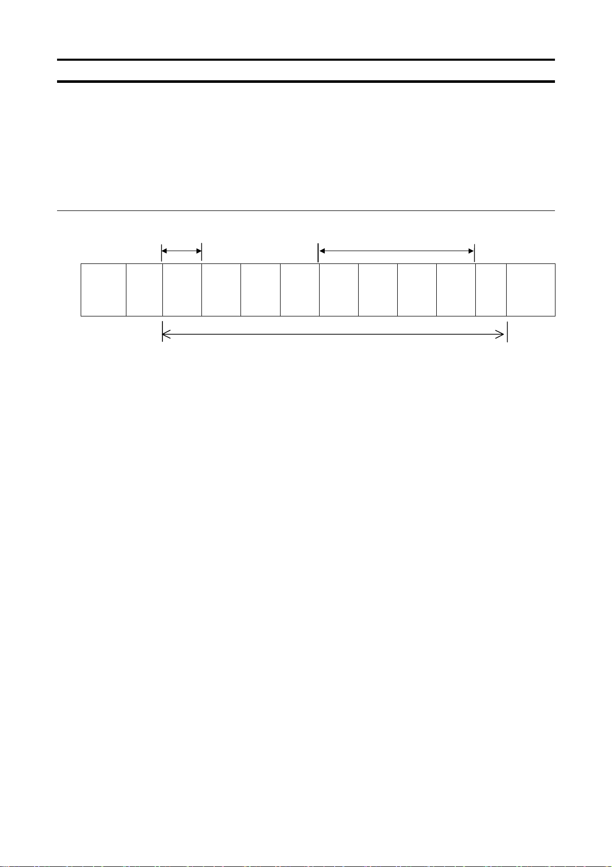
(HEX) code, in addition to the JIS (ASCII) code. A communication number is used to access the desired data item.
* The smallest unit of information that computers handle is called a “bit (binary digit),” which repre-
sents the two numbers in the binary system: 1 or 0. A group of 16 bits is referred to as a “word,”
which is the basic unit of information the VF-AS1 series of inverters use for data communication.
One word can handle data items of 0 to FFFFH in hexadecimal notation (or 0 to 65535 in decimal
notation).
BIT15 BIT8BIT7 BIT0
1 bit
1 word
3
Page 5

2. Data transmission specifications
Items Specifications
Transmission scheme Half-duplex
Synchronization scheme Start-stop synchronization
Communication baud rate 9600/19200*/38400 bps (selectable using a parameter)
*1
Communication protocol TOSHIBA Inverter Protocol * / MODBUS-RTU (selectable using a parameter)
Character transmission <ASCII mode> JIS X 0201 8-bit (ASCII)
<Binary mode, MODBUS-RTU> Binary codes fixed to 8 bits
Stop bit length Received by inverter: 1 bit, Sent by inverter: 2 bits
*3
Error detecting scheme Parity *2: Even */Odd/Non parity (selectable using a parameter) *1,
checksum(Toshiba inverter protocol), CRC(MODBUS-RTU)
Character transmission
11-bit characters *1 (Stop bit=1, with parity)
format
Order of bit transmission Low-order bits transmitted first
Frame length Variable (to a maximum of 17 bytes)
*1: Changes to setting do not take effect until the inverter is turned back on or reset.
*2: JIS-X-0201 (ANSI)-compliant 8-bit codes are used for all messages transmitted in ASCII mode
and vertical (even) parity bits specified by JIS-X-5001 are added to them. These even parity bits
can be changed to odd parity bits by changing the parameter setting (a change to the parameter
setting does not take effect until the inverter has been reset.)
*: Standard
default setting
E6581315
*1
*3: Here are the default character transmission format.
Characters received: 11 bits (1 start bit + 8 bits + 1 parity bit + 1 stop bit)
START
BIT BIT0BIT1BIT2BIT3BIT4BIT5BIT6BIT7
The inverter receives one stop bit.
(The computer can be set so as to send 1, 1.5 or 2 stop bits.)
Characters sent: 12 bits (1 start bit + 8 bits + 1 parity bit + 2 stop bits)
START
BIT BIT0 BIT1
BIT2 BIT3 BIT4 BIT5 BIT6 BIT7
The inverter sends two stop bits.
(The computer can be set so as to receive 1, 1.5 or 2 stop bits.)
PARITY
BIT
PARITY
BIT
STOP
BIT
STOP
BIT
STOP
BIT
4
Page 6

3. Communication protocol
This communication protocol supports the TOSHIBA Inverter Protocol and part of MODBUS-RTU
protocol.
Select the desired protocol from in the following communication protocol selection parameters
(, ).
“Parameter Name and , Communication Number. 0807 and 0829”
Data Range: 0, 1 (Initial value: 0)
0: TOSHIBA (Includes inter-drive communication)
1: MOUBUS-RTU
* A parameter change is reflected when the inverter is reset, such as in power off.
3.1. About the handling of received frames
To send and receive data frames, a frame synchronization system for locating the start and end
points of each frame is defined with time for which no data is sent (time interval equivalent to the
time required to send 3.5 bytes of data).
If no data is sent for the time required to send 3.5 bytes of data at the current transmission speed
(approx. 4 ms or more at 9,600 bps or approx. 2 ms or more at 19,200/38,400 bps) after receipt of a
frame, the entire frame is assumed to have reached and information in it is analyzed. For this reason, an interval corresponding to at least 3.5 bytes of data must be placed between frames.
When sending a significant data set using two or more frames, an interval corresponding to at least
1.5 bytes of data must be placed between frames. If an interval corresponding to 1.5 bytes or more
is not placed, the contents of a frame are analyzed separately from those of the other frames, and
therefore communication are not carried out normally.
When two or more inverters on the same line are controlled individually one after another, not only
data from the host computer to an inverter but also a response from an inverter to the host computer
are transmitted to the other inverters on the line too. Therefore, an interval corresponding to at least
3.5 bytes should be placed between the time when the host computer receives a response from an
inverter and the time when it sends a frame to the next inverter. Otherwise the return frame received
and the frame that is sent immediately after receipt of the return frame will be recognized as one
frame and communication will not be carried out normally.
E6581315
[Correct]
Frame A
[Wrong] If divided into two smaller frames, frame A cannot be received as a
single frame.
Frame A (1/2)
1.5 bytes or more
5
3.5 bytes or more
Frame A (2/2)
Note: Correct if the interval corresponds
to less than 1.5 bytes of data.
Note: An inverter cannot receive frame
B before it finishes analyzing the
contents of frame A.
Frame B
Frame B
Page 7

4. TOSHIBA Inverter Protocol
Select “TOSHIBA” (, =) in the communication protocol selection parameters.
“TOSHIBA” (, =) is set for initial communication protocol selection of shipment
setting. (See “3. Communication protocol.”)
Exchange of data between the computer and the inverter
In communication between the computer and the VF-AS1 (hereinafter referred to as the inverter),
the inverter is always placed in wait states and acts as a slave that operates on a request from the
computer.
A discrimination between ASCII mode and binary mode is automatically made with the start code.
ASCII mode “(” Required
Binary mode “2FH(/) ” Not required
(1) If there is no transmission format or the inverter number that matches, an error occurs and no
response is returned.
E6581315
Start code “CR” (carriage return)
Note
(2) When an inverter number is added behind the “(” communication will take place only in case of
broadcast communication or if the number matches up with that assigned to the inverters.
(3) When a time-out period is specified with parameter f803 (communication time-out time), a
time-out occurs if communication do not terminate normally within the specified time. With
parameter f804 (communication time-out action), you can specify what the inverter should do
if a time-out occurs. For details, refer to Section 7.3.
(4) On executing the command received, the inverter returns data to the computer. For the response
time, see Appendix 2, “Response time.”
Communication is not possible for about two seconds after the power is supplied to the inverter until
the initial setting is completed. If the control power is shut down due to an instantaneous voltage
drop, communication is temporarily interrupted.
6
Page 8

4.1. Data transmission format
Note: The term “trip status” used in this manual includes retry waiting status and trip retention status.
4.1.1. Data transmission format used in ASCII mode
A communication number is used to specify a data item, all data is written in hexadecimal, and JISX-0201 (ASCII (ANSI))-compliant transmission characters are used.
Computer → Inverter
Omissible in one-to-one communication For the W and P commands only Omissible
E6581315
(3.5bytes
Blank)
Omissible
"("
(28H)
Checksum area
1. “(“ (1 byte) : Start code in ASCII mode
2. INV-NO (2 bytes) : Inverter number (Omissible in one-to-one communication) ... 00 (30H, 30H) to 99 (39H,
3. CMD (1 byte) : Command (For details, see the table below.)
4. Communication No.(4 bytes)
5. Data (0 to 4 bytes): Write data (valid for the W and P commands only)
6. “&” (1 byte) : Checksum discrimination code (omissible. When omitting this code, you also need to omit
INV-NO
2 bytes
CMD
1 byte
39h), *(2AH)
The command is executed only when the inverter number matches up with that specified
using a parameter.
(When * is specified in broadcast communication, the inverter number is assumed to match
if all numbers except * match. When * is specified instead of each digit (two-digit number),
all inverters connected are assumed to match.)
If the inverter number does not match or if the inverter number is of one digit, the data will
be judged invalid and no data will be returned.
: Communication number (See 11, “Parameter data.”)
the checksum.)
Communication No.
4 bytes
DATA
0 to 4 bytes
"&"
(26H)
SUM
2 bytes
")"
(29H)
CR
(0DH)
(3.5bytes
Blank)
7. Sum (2 bytes) : Checksum (omissible)
Add the ASCII-coded value of the last two digits (4 bits/digit) of the sum of a series of bits
(ASCII codes) from the start code to the checksum discrimination code.
Ex.: (R0000&??) CR
28H+52H+30H+30H+30H+30H+26H=160H
The last two digits represent the checksum. = 60
When omitting the checksum, you also need to omit the checksum discrimination
code.
8. “)” (1 byte) : Stop code (omissible)
9. CR (1 byte) : Carriage return code
Details of commands and data
CMD (1 byte) Write data (0 to 4 bytes) Hexadecimal number
R (52H): RAM read command
W (57H): RAM/EEPROM write command
P (50H) RAM write command
No data
Write data (0 to FFFF)
Write data (0 to FFFF)
7
Page 9

Inverter → computer
At time of broadcast communication, returning of data is not executed, except for the inverters to be
returned, when the inverter number is not matched, and the inverter number has only one character.
This is because there will be a risk of that the returned data may be deformed.
Data returned when data is processed normally (ASCII mode)
Omissible in one-to-one communication Omissible
E6581315
(3.5bytes
Blank)
Omissible
"("
(28H)
Checksum area
1. “(“ (1 byte) : Start code in ASCII mode
2. INV-NO (2 bytes) : Inverter number (omitted if it is not found in the data received) ... 00 (30H, 30H) to 99 (39H,
3. CMD (1 byte) : Command ... The command is also used for a check when an inverter is tripped.
4. Communication No.(4 bytes) :
INV-NO
2 bytes
CMD
1 byte
39H)
If the inverter number matches up with that specified using a parameter, data will be returned to the computer. In broadcast communication, only the destination inverter (with a number matching up with the smallest effective number) returns data to the computer.
In broadcast communication, no data is returned from any inverters except the inverter
bearing a number that matches up with the smallest effective number.
Ex.: (*2R0000) CR -> (02R00000000) CR)
Under normal conditions... The uppercase letter R, W or P is returned, depending on the
command received: R, W or P command.
When an inverter is tripped... The lowercase letter r, w or p is returned, depending on the
command received: R, W or P command.
(The command received is returned with 20H added to it.)
The communication number received is returned.
Communication No.
4 bytes
Data is returned from the inverter with the number 2 only, but no data is returned from
inverters with the number 12, 22 ....
DATA
0 to 4 bytes
"&"
(26H)
SUM
2 bytes
")"
(29H)
CR
(0DH)
(3.5bytes
Blank)
5. Data (0 to 4 bytes): Data ... The data read in is returned for the R command, while the data received is returned
for the W and P commands. If the data received is composed of less than 4 digits, it will be
converted into 4-digit data and returned.
Ex.: (W123412) CR → (W12340012) CR)
6. “&” (1 byte) : Checksum discrimination code (omitted if it is not found in the data received)
7. Sum (2 bytes) : Checksum ... Omitted if no checksum discrimination code is found in the data received.
ASCII-coded value of the last two digits (4 bits/digit) of the sum of a series of bits (ASCII
codes) from the start code to the checksum discrimination code.
8. “)” (1 byte) : Stop code (omitted if it is not found in the data received)
9. CR (1 byte) : Carriage return code
8
Page 10

• Data returned when data is not processed normally (ASCII mode)
In case an error occurs, communication error command (4EH(N) or 6EH(n)) and the error type number is returned to the computer in addition to the checksum. At time of broadcast communication of
the binary mode, returning of data is not executed except for the inverter to be returned (inverter
number 00H) and when the inverter number is not matched. This is because there will be a risk that
the returned data may be deformed.
Omissible Omissible
E6581315
(3.5bytes
Blank)
“(“
(28H)
INV-NO
2 bytes
“N” or “n”
(4EH) (6EH)
DATA
4 bytes
"&"
(26H)
SUM
2 bytes
Checksum area
Omissible
“(“ (1 byte) : Start code in ASCII mode
“N” or “n” (1 byte) :Communication error command ... This is also used for the checking of inverter trip.
“N” for the normal communication and “n” during the inverter trip.
INV-NO (2 bytes) : Inverter number (omitted if it is not found in the data received) ... 00 (30H, 30H) to 99 (39H,
39H)
If the inverter number matches up with that specified using a parameter, data will be returned to the computer. In broadcast communication, only the destination inverter (with a number matching up with the smallest effective number) returns data to the computer.
Data (4 bytes) : Error code (0000~0004)
0000 ... Impossible to execute (Although communication is established normally, the
command cannot be executed because it is to write data into a parameter whose
setting cannot be changed during operation (e.g., maximum frequency) or the
EEPROM is faulty.)
0001 ... Data error (The data is outside the specified range or it is composed of too many
digits.)
0002 ... Communication number error (There is no communication number that matches.)
0003 ... Command error (There is no command that matches.)
0004 ... Checksum error (The checksum result differs.)
")"
(29H)CR(0DH)
(3.5bytes
Blank)
“)” (1 byte) : Stop code ... This code is omitted if it is not found in the data received.
Examples:
(N0000&5C)CR... Impossible to execute (e.g., a change of maximum frequency data during opera-
tion)
(N0001&5D)
(N0002&5E)
(N0003&5F)
... Data error (Data is outside the specified range.)
CR
... No communication number (There is no communication number that matches.)
CR
... There is no command that matches. (Commands other than the R, W and P
CR
commands)
(Ex.: L, S, G, a, b, m, r, t, w ...)
(N0004&60)
... Checksum error (The checksum result differs.)
CR
No data returned ... Format error or invalid inverter number
9
Page 11

4.1.2. Data transmission format used in binary mode
A communication number is used to specify a data item, data is written in hexadecimal form, and
data in transmission characters are represented by binary codes (HEX codes).
Computer → Inverter (binary mode)
Omissible in one-to-one communication No data for the 52H (R) command
E6581315
(3.5bytes
Blank)
1. 2FH (“/”) (1 byte) : Start code in binary mode
2. INV-NO (2 bytes) : Inverter number (Omissible in one-to-one communication) ... 00H to 3FH ,FFH
3. CMD (1 byte) : Command (For details, see the table below.)
4. Communication No.(2 bytes)
5. Data (2 bytes) : 0000H to FFFFH
“/”
INV-NO
(2FH)
Checksum area Not omissible
1 byte
CMD
1 byte
In case the inverter number is other than FFH (broadcast communication), command is ex-
ecuted only when the inverter number coincides with the one designated with the panel. If
the inverter number is not matched, it will be judged invalid and the data is not returned.
52H (R) command: The size of the data following CMD is fixed to 3 bytes. (Communication
number: 2 bytes, checksum: 1 byte)
57H (W), 50H (P) and 47H (G) commands: The size of the data following CMD is fixed to 5
bytes.
(Communication number: 2 bytes, data: 2 byte, checksum: 1 byte)
Any command other than the above is rejected and no error code is returned.
: Communication number (See 11, “Parameter data.”)
57H (W) and 50H (P) commands: Write data (An area check is performed.)
47H (G) command: Dummy data (e.g., 0000) is needed.
52H (R) command: Any data is judged invalid. (No data should be added.)
Communication No.
2 bytes
DATA
2 bytes
SUM
1 byte
(3.5bytes
Blank)
6. Sum (2 bytes) : Checksum (not omissible) 00H to FFH
Value of the last two digits (1 byte) of the sum of a series of bits (codes) from the start code
of the data returned to the data (or to the communication number for the 52H (R) command)
Ex.: 2F 52 00 ?? ... 2FH+52H+00H+00H=81H
The last two digits (??) represent the checksum= 81
Details of commands and data
CMD (1 byte) Write data (2 bytes) Hexadecimal number
52H (R): RAM read command
57H (W): RAM/EEPROM write command
50H (P): RAM write command
47H (G): RAM read command (for two-wire networks)
No data
Write data (0000H to FFFFH)
Write data (0000H to FFFFH)
Dummy data (0000H to FFFFH)
10
Page 12

Inverter → computer (binary mode)
At time of broadcast communication of the binary mode, returning of data is not executed except for
the inverter to be returned (inverter number 00H) and when the inverter number is not matched. This
is because there will be a risk that the returned data may be deformed.
• Data returned when data is processed normally (Binary mode)
Omissible
E6581315
(3.5bytes
Blank)
1. 2FH (“/“) (1 byte) : Start code in binary mode
2. INV-NO (2 bytes) : Inverter number... 00H to 3FH (The inverter number is omitted if it is not found in the data
3. CMD (1 byte) : Command...The command is also used for a check when the inverter is tripped.
4. Communication No. (4 bytes)
5. Data (2 bytes) : Data ... 0000H to FFFFH
6. Sum (1 bytes) : Checksum (not omissible) 00H to FFH
“/”
INV-NO
(2FH)
Checksum area Not omissible
1 byte
CMD
1 byte
received.)
If the inverter number matches up with that specified from the operation panel, data will be
returned from the inverter. If the inverter number does not match, the data will be invalid
and no data will be returned.
Under normal conditions...52H (R), 47H (G), 57H (W) or 50H (P) is returned, depending on
the command received.
When the inverter is tripped...The lowercase letter 72H (r), 67H (g), 77H (w) or 70H (p) is
returned with 20H added to it, depending on the command received.
: The communication number received is returned.
The data read is returned for the 52H (R) and 47H (G) commands, while the data written is
returned for the 57H (W) and 50H (P) commands.
Value of the last two digits (1 byte) of the sum of a series of bits (codes) from the start code
to the data.
Communication No.
2 bytes
DATA
2 bytes
SUM
1 byte
(3.5bytes
Blank)
11
Page 13

2) Error Processing (Binary mode)
In case an error occurs, communication error command (4EH(N) or 6EH(n)) and the error type number is returned to the computer in addition to the checksum. At time of broadcast communication of
the binary mode, returning of data is not executed except for the inverter to be returned (inverter
number 00H) and when the inverter number is not matched. This is because there will be a risk that
the returned data may be deformed.
Omissible
(3.5bytes
Blank)
Norn (1 byte) : Communication error command ... This command is also used for a check when the in-
Data (2 bytes) : Error code (0000~0004)
“/”
INV-NO
(2FH)
Checksum area Not omissible
1 byte
verter is tripped.
“4EH (N)” is returned under normal conditions, while “6EH (n)” is returned when the in-
verter is tripped.
0000 ... Impossible to execute (Although communication is established normally, the com-
mand cannot be executed because it is to write data into a parameter whose setting cannot be changed during operation (e.g., maximum frequency) or the
EEPROM is faulty.)
0001 ... Data error (The data is outside the specified range or it is composed of too many
digits.)
0002 ... Communication number error (There is no communication number that matches.)
0004 ... Checksum error (The checksum result differs.)
Norn
(4EH)(6EH)
DATA
2 bytes
SUM
1 byte
(3.5bytes
Blank)
E6581315
Examples:
No code returned ...Command error, format error (failure to receive the specified number of
bytes within 0.5 seconds, or an parity, overrun or framing error) or the
inverter number does not match or an inverter in broadcast communication in the binary mode except for the inverter for data returning (the
inverter numbered 00H).
2FH, 4EH, 00H, 00H, 7DH ... Impossible to execute (e.g., a change of maximum frequency data
during operation)
2FH, 4EH, 00H, 01H, 7EH ... Data setting error (The data specified falls outside the specified
range.)
2FH, 4EH, 00H, 02H, 7FH ... No communication number (There is no communication number that
matches.)
2FH, 4EH, 00H, 04H, 81H ... Checksum error (The checksum result differs.)
12
Page 14
4.1.3. Transmission format of Block Communication
What is block communication?
Data can be written in and read from several data groups set in one communication by setting the
type of data desired for communication in the block communication parameters (, ,
to ) in advance. Block communication can save the communication time.
Data is transmitted hexadecimal using the binary (HEX) code transmission characters. “Computer
→ inverter” is for writing only, while “Inverter → computer” for reply is for reading only.
Computer → Inverter (Block Communication)
E6581315
Number of writing data groups x 2 bytes
Number of
read
data
groups
Write
data1
High
Write
data1
Low
Write
data2
High
Write
data2
Low
(3.5bytes
Blank)
Start
Code
“/”
Omissible
INV-NO CMD
“X”
Num-
ber of
write
data
groups
Checksum Area
1. 2FH(“/”) (1 byte) : Start code of binary mode
2. INV-NO (1 byte) : Inverter number. (Can be omitted in 1:1 communication): 00H to 3FH, FFH
Executed only when the inverter number matches the inverter number. Set on the panel, except in FFH (broadcast communication).
Communication data will be invalidated and data will not be returned either if the inverter
number. Does not match.
3. CMD (1 byte) : ‘X’ (Block communication command)
4. Number of write data groups (1 byte)
: Specify the number of data groups to be written (00H to 02H).
If specified outside of the range, data will be treated as a format error and data will not be returned.
5. Number of read data groups (1 byte)
: Specify the number of data groups to be read (00H to 05H).
If specified outside of the range, data will be returned as “Number of read data groups = 0”
when returned by the inverter.
SUM
(3.5bytes
Blank)
6. Write data1 (2 bytes)
: Needed when the number of write data groups is larger than 1.
Data to be written to the specified parameter selected by
Dummy data is needed if the number of write data groups is larger than 1 even though(none)
is selected for
7. Write data2 (2 bytes)
: Needed when the number of write data groups is 2.
Data to be written to the specified parameter selected by
Dummy data is needed if the number of write data groups is 2 even though(none) is selected
for
8. SUM (1 byte) : Checksum (Cannot be omitted) 00H to FFH
Lower two digits (1 byte) of total sum from start code (SUM value not included)
13
Page 15

E6581315
Block Write 1, 2
Select data, which is desired to be written in block communication, in block write Data 1 and 2 Parameters (, ). This parameter becomes effective when the system is reset, such as
when power is turned off. When the setting is completed, turn off and then on the power.
No. Block Write Data For data details, see:
0 Deselect −
1 Command information 1 (FA00)
2 Command information 2 (FA20)
3 Frequency Command (FA01)
4 Terminal board output data (FA50)
5 Communication analog output (FA51)
* When “Deselect” is specified in the parameters, no data will be written even though write data is
specified.
Block Read 1 to 5
Select read data, which is desired to be read in block communication, in block read data 1 and 5 Parameters (to). This parameter becomes effective when the system is reset,
such as when power is turned off. When the setting is completed, turn off and then on the power.
“8.1 Command by communication”
No. Block Read Data For data details, see:
0 Deselect −
1 Status information (FD01)
2 Output frequency (FD00)
3 Output current (FD03)
4 Output voltage (FD05)
5 Alarm Information (FC91)
6 PID feedback value (FD22)
7 Input terminal board monitor (FD06)
8 Output terminal board monitor (FD07)
9 V/II terminal boad monitor (FE36)
10 RR/S4 terminal board monitor (FE35)
11 RX terminal board monitor (FE37)
12 Input voltage (DC detection) (FD04)
13 Speed feedback frequency (FD16)
14 Torque (FD18)
15 My monitor 1(FE60) −
16 My monitor 2(FE61) −
17 My monitor 3(FE62) −
18 My monitor 4(FE63) −
19 Free notes (F880) “7.5 Free notes ()”
* V/II terminal board monitor (FE36), RR/S4 terminal board monitor (FE35) and RX terminal board
monitor (FE37) will become hold data during a trip. Otherwise, real-time data appears.
* “0000” will be returned as dummy data, if “0 (Deselect)” is selected for the parameter and “read” is
specified.
“8.2 Monitoring from communication”
14
Page 16
Inverter → Computer
At time of broadcast communication of the binary mode, returning of data is not executed except for
the inverter to be returned (inverter number 00H) and when the inverter number is not matched. This
is because there will be a risk that the returned data may be deformed.
1) Normal processing
E6581315
(3.5
bytes
Blank)
Omissible
Start
Code
“/”
INV
No.
CMD
“Y”
Number
of Read
Data
Groups
Write
Status
Read
data1
high
Number of read data groups x 2 bytes
Read
Read
Read
Read
data3
data2
data2
data1
high
low
high
low
Checksum area
1. 2FH “/” (1 byte) :Start code in binary mode
2. INV-NO (1Byte) :Inverter number・・・00H to 3FH
If the inverter number matches up with that specified from the operation panel, data will
be returned from the inverter. If the inverter number does not match, the data will be
judged invalid and no data will be returned.
Communication data will be invalidated and data will not be returned either if the inverter number does not match. (Inverter number is considered matched if it is omitted
during reception)
3. CMD(1Byte) :‘Y’ (Block communication command [monitoring])
Lowercase letter ‘y’ during an inverter trip, including standing by for retrying and during
a trip.
4. Number of read data groups (1 byte)
: Return the number of data groups to be read (00H to 05H).
5. Write status (1 byte) : Return 00H to 03H.
* Failing to write in the specified parameter in the number of write data groups, set “1”
in the corresponding bit for the parameter failed to write. (See below.)
Read
data3
low
Read
data4
high
Read
data4
low
Read
data5
high
Read
data5
low
SUM (3.5
bytes
Blank)
Bit Position 7 6 5 4 3 2 1 0
Data Type −
6. Read data1 - 5 (2 bytes)
: Return according to the number of read data groups. “0000H” is returned as dummy
data if “0” is selected as a parameter.
Read data1: Data selected by . Read data2: Data selected by .
Read data3: Data selected by . Read data4: Data selected by .
Read data5: Data selected by .
7.SUM(1Byte) : Checksum (Cannot be omitted) 00H to FFH
Lower two digits (1 byte) of total sum from start code of return data to read data.
Example
(When set as follows: = (Command information 1), = (frequency command),
= (status information), = (output frequency), = (output current), = (output
voltage) and = (alarm information)
Computer → Inverter:2F 58 02 05 C4 00 17 70 D9
Inverter → Computer:2F 59 05 03 00 00 00 00 00 00 00 00 00 00 90 (When parameter is not set)
Inverter → Computer:2F 59 05 00 40 00 00 00 00 00 00 00 00 00 CD CD (When parameter is set)
Inverter → Computer:2F 59 05 00 64 00 17 70 1A 8A 24 FD 00 00 3D (During operation at 60Hz)
15
Page 17

2) Error Processing (Binary mode)
In case an error occurs, communication error command (4EH(N) or 6EH(n)) and the error type number is returned to the computer in addition to the checksum.
Omissible
(3.5bytes
Blank)
“N” or “n” (1 byte) : Communication error command. Also for check during an inverter trip (includes standing
DATA (2 bytes) : Error code (0004)
“/”
INV-NO
(2FH)
Checksum area Not omissible
0004 : Checksum error (The checksum does not match)
No return : Command error, format error (specified number of bytes is not received in 1sec,
1 byte
by for retrying and trip holding). “4EH (N)” when normal, “6EH (n)” during an inverter trip.
or parity error, overrun error or framing error), inverter number mismatch, and
inverter number other than 00H in broadcast communication.
Norn
(4EH)(6EH)
DATA
2 bytes
SUM
1 byte
(3.5bytes
Blank)
E6581315
Examples
Computer → Inverter : 2F 58 02 05 C4 00 17 70 D8
Inverter → Computer : 2F 4E 00 04 81 ... Checksum error
16
Page 18

4.2. Commands
Here are the communication commands available.
Command Function
R command Reads the data with the specified communication number.
W command Writes the data with the specified communication number. (RAM and EEPROM).
P command Writes the data with the specified communication number. (RAM).
G command
X command Block communication (Computer -> Inverter)
Y command Block communication (Inverter -> Computer)
E6581315
Reads the data with the specified communication number. (For binary mode only.
Dummy data is required for this command.)
W (57H) (RAM
This command is used to write new data into the parameter specified using it communication number. It writes data into the RAM and EEPROM. For parameters whose settings cannot be stored in
the EEPROM (e.g., parameter with the communication number FA00), the W (57H) command writes
data into the RAM only. It cannot be used to write data into read-only parameters (e.g., parameter
with the communication number FD?? or FE??).
Each time an attempt to write data is made, the inverter checks if the data falls within the specified
range. If this check reveals that the data falls outside the specified range, the inverter will reject it
and return an error code.
- Ex.: Setting the deceleration time (communication number: 0010) to 10 sec.
<ASCII mode>
<Binary mode>
♦ Do not write the same parameter to the EEPROM more than 10,000 times. The life time of EEPROM is
approximately 10,000 times.(Some parameters are not limited, please refer to the “9.Parameter data “)
The lifetime of EEPROM is approximately 10,000 times. When using the TOSHIBA inverter protocol and
the data does not need to be records, use P command (the data is written only to RAM).
*1
/EEPROM*2 write)
CR: Carriage return
Computer → Inverter Inverter
(W00100064)CR (W00100064)CR …(10÷0.1=100=0064H)
Computer → Inverter Inverter
2F 57 00 10 00 64 FA 2F 57 00 10 00 64 FA …(10÷0.1=100=0064H)
→ Computer
→ Computer
Notice
Explanation of terms
*1: The RAM is used to temporarily store inverter operation data. Data stored in the RAM is cleared
*2: The EEPROM is used to store inverter operation parameter settings, and so on. Data stored in
when the inverter is turned off, and data stored in the EEPROM is copied to the RAM when the
inverter is turned back on.
the EEPROM is retained even after the power is turned off, and it is copied to the RAM when the
inverter is turned on or reset.
17
Page 19

E6581315
P (50H) (RAM
*1
write)
This command is used to rewrite data into the parameter specified using a communication number.
It writes data into the RAM only. It cannot be used to write data into any read-only parameters. Each
time an attempt to write data is made the inverter checks whether the data falls within the specified
range. If this check reveals that the data falls outside the range, the inverter will reject it and return
an error code.
- Ex.: Entering the emergency stop command (communication number: FA00) from the computer
<ASCII mode>
Computer → Inverter Inverter
(PFA009000)CR (PFA009000)CR …Command priority, emergency stop
<Binary mode>
Computer →
2F 50 FA 00 90 00 09 2F 50 FA 00 90 00 09
R (52H) (Data read)
This command is used to read the setting of the parameter specified using a communication number.
- Ex.: Monitoring the electric current (communication number: FE03)
<ASCII mode>
Computer →
(RFE03)CR (RFE03077B)CR …Current: 1915 / 100 = 19.15%
<Binary mode>
Computer →
2F 52 FE 03 82 2F 52 FE 03 07 7B 04
→ Computer
command
Inverter Inverter → Computer
Inverter Inverter → Computer
Inverter Inverter → Computer
G (47H) (Data read)
This command is used to read the parameter data specified using a communication number. Although this command is used for the previous model to control the operation of two or more inverters
in binary mode through a two-wire RS485 network, the “R” command can also be used without
problems for the VF-AS1 series.
To use the “G” command, however, dummy data (2 bytes) is needed.
This command is available only in binary mode.
- Ex.: Monitoring the electric current (communication number: FE03)
Computer → Inverter Inverter
2F 47 FE 03 00 00 77 2F 47 FE 03 07 7B F9
* In this example, the data 00H sent from the computer to the inverter is dummy data.
→ Computer
S (53 H)/ s (73 H) Inter-drive communication command(RAM
This command is for using frequency command values in % (1 = 0.01%), instead of in Hz, and is for
synchronous-proportional operation in inter-drive communication. This command can also be
used in ordinary computer link communication.
When writing in the frequency command (FA01, FA05) is enabled and a parameter other than it is
specified, a communication number error will result. Data is written in the RAM only and at this
time the data check such as an upper limit and lower limit checking is not carried out.
Data is not returned from the inverters while this command is used. This command can be used
only in the binary mode.
For the details of the format, see “6.2 Transmission format for inter-drive communication.”
Use (%) as the unit for frequency command values specified by the command S, instead of (Hz),
and the receiving side converts units for frequency values to “Hz” in accordance with the point conversion parameter. The conversion formula is shown below.
*1
Write)
Frequency command value (Hz) =
Point 2 frequency (F813) − Point 1 frequency (F812)
Point 2 (F814) − Point 1 (F811)
− Point 1 (F811) + Point 1 frequency (F812)
18
x (Frequency command value (%)
Page 20

E6581315
When Command “s” (lowercase letter) is received, the slave side judges that the master side is
tripped and operates in accordance with the inter-drive communication parameter (,
).
For detail, see "7. Communication parameters ".
- Examples: 50% frequency command (2-wire RS485 communication)
(If maximum frequency = Frequency for operation at 80Hz = 40Hz: 50% = 5000d = 1388H)
<Binary mode>
Master inverter → Slave inverter Slave inverter
2F 53 FA 01 13 88 18 No return
X(58H)/Y (59H) (Block Communication Command)
Data selected in the block communication write parameters (,) is written in the
RAM. When returning data, data selected in block communication read parameters ( to
) is read and is returned.
For detail, see "4.1.3. Transmission format of Block Communication ".
- Examples: 60Hz operation command from communication and monitoring (Monitoring when al-
ready operating at 60Hz)
(Parameter Setting:
, =
<Binary mode>
Computer → Inverter Inverter
2F 58 02 05 C4 00 17 70 D9 2F 59 05 00 64 00 17 70 1A 8A 24 FD 00 00 3D
= , = , = , = , = , =
)
→ Master inverter
→ Computer
19
Page 21

4.3. Transmission errors
Table of error codes
Error name Description Error code
E6581315
Impossible to exe-
cute
The command is impossible to execute, though communication was
established normally.
0000
1 Writing data into a parameter whose setting cannot be changed
during operation (e.g., maximum frequency)
*1
2 Writing data into a parameter while “” is in progress
Data error Invalid data is specified. 0001
Communication
There is no communication number that matches. 0002
number error
Command error The command specified does not exist. 0003 (ASCII mode)
No code returned (Binary
mode)
Checksum error The Checksum does not match. 0004
Format error The data transmission format does not match.
No code returned
1 One-digit inverter number (ASCII mode)
2 The CR code is found in the designated position. (ASCII mode)
Ex.:Communication number of 4 digit or less. In the case of (R11)
CR, 11) CR is recognized as a communication number and
the CR code is not recognized, with the result that a format
error occurs.
3 A code other then the stop code (“)”) is entered in the stop code
position.
Receiving error A parity, overrun or framing error has occurred.
*2
No code returned
*1: For parameters whose settings cannot changed during operation, see ”Table of parameters.”
*2: Parity error : The parity does not match.
Overrun error : A new data item is entered while the data is being read.
Framing error : The stop bit is placed in the wrong position.
* For the errors with “no code returned” in the above table, no error code is returned to avoid a data
crash.
If no response is received, the computer side recognizes that a communication error has occurred.
Retry after a lapse of some time.
* If the inverter number does not match, no processing will be carried out and no data will be re-
turned, though it is not regarded as an error.
20
Page 22

4.4. Broadcast communication function
Broadcast communication function can transmit the command (write the data) to multiple inverters
by one communication. Only the write (W, P) command is valid and the read (R, G) command is invalid. The inverters subject to the broadcast communication are the same to the independent communication; 0 to 99 (00H - 63H) in the ASCII mode, and 0 to 63 (00H - 3FH) in the binary mode. To
avoid data deforming, the inverters to return data will be limited.
“Overall” broadcast communication (ASCII mode / Binary mode)
- ASCII Mode
If you enter two asterisks (**) in the inverter number position of the data transmission format, the
computer will send the data simultaneously to all inverters (with an inverter number between 0 and
99 (00 to 63H)) on the network.
- Binary Mode
To put "FF" to the specified place of the inverter number in the communication format validates the
broadcast communication and the command is transmitted to all the applicable inverters in the net-
work (inverter numbers from 0 to 63 (00 to 3FH)).
<Inverter that returns data to the computer>
Data is returned from the inverter bearing the inverter number 00 only.
If you do not want inverters to return data, do not assign the number 00 to any inverter on the network.
E6581315
“Group” broadcast communication (ASCII mode only)
If you put “*?” In the inverter number position of the data transmission format, data will be sent
simultaneously to all inverters bearing a number whose digit in the one’s place in decimal notation
is”?”
If you put ”?*” In the inverter number position of the data transmission format, the data will be sent
simultaneously to all inverters bearing a number whose digit in the ten’s place in decimal notation
is”?”.
(“?”: Any number between 0 and 9.)
<Inverter that returns data to the computer>
Data is returned only from the inverter bearing the smallest number in the same group of inverters
(i.e., inverter whose number in the position of ”*” is 0).
If you do not want inverters to return data to the computer, do not assign a number having a 0 in the
position of “*” to any inverter on the network.)
Examples of broadcast communication
Ex: Set the frequency setting for communication to 60Hz.
1 Host computer → Multiple inverters: broadcast communication (ASCII Mode)
Example of transmission of data from host computer to inverter: (**PFA011770)
Example of data returned from inverter to host computer: (00PFA011770)
Data is returned from the inverter numbered 00 only, while commands are issued to all inverters
connected to the network.
2 Host computer → A specific group of inverters: group communication (ASCII Mode)
Example of transmission of data from host computer to inverters: (*9PFA011770)
Example of data returned from inverter to host computer: (09PFA011770)
Data is returned only the inverter numbered 09 only, while commands are issued to a maximum
of 10 inverters bearing the number 09, 19, 29, 39, ... or 99.
CR
CR
CR
CR
21
Page 23

Host
computer
E6581315
Block 1
Inverter No. 10 Inverter No.11 Inverter No.19
VF-AS1
VF-AS1 VF-AS1 VF-AS1 VF-AS1 VF-AS1
*1
Inverter No.20 Inverter No.21 Inverter No.29
Block 2
*1: Error signal I/F
In broadcast communication, only the representative inverter in each block returns data to the host
computer. However, you can make the representative inverter in each block report the occurrence of
a problem in the block. To do so, follow these steps.
Set the timer function so that, if a time-out occurs, the inverter will trip (Ex.: = (sec)), set
the output terminal selection parameter (FL) so that trip information will be output through the output
terminal (=), and set the input terminal selection parameter (F) of the representative inverter in each block to “external input trip (emergency stop)” (=). Then, connect the input
terminal (F, CC) of the representative inverter to the FL terminal (FLA, FLC) of each of the other inverters in the same block (FLA-F, FLC-CC). In this setting, if an inverter trips, the representative inverter will come to an emergency stop, and as a result it will report the occurrence of a problem in its
block to the computer. (If the representative inverter returns a lowercase letter in response to a
command from the computer, the computer will judge that a problem has arisen in an inverter.) To
examine details on the problem that has arisen, the host computer accesses each individual inverter,
specifying its communication number. To make the computer issue a command to all inverters in
block 1 or block 2 shown in the figure above, specify “1*” or “2*”, respectively. In this system, inverter
No. 10 will return data to the computer if a problem arises in block 1, or inverter No. 20 if a problem
arises in block 2. For overall broadcast communication, specify “**”, in which case the inverter with
the communication number “00” will return data to the computer.
In this example, if you want the computer to maintain communication without bringing an representative inverter to an emergency stop, set its input terminal selection parameter to “disabled
(=) but not to “external input trip (emergency stop).” This setting causes the host computer
to check the setting of the input terminal information parameter (Communication No.=DF06, bit 0) of
the representative inverter, and as a result enables the computer to detect the occurrence of a
problem.
CAUTION:
Data from inverters will be deformed if inverters of the same number are connected on the network.
Never assign same single numbers to inverters on the network.
22
Page 24

4.5. Examples of the use of communication commands
Here are some examples of the use of communication commands provided for the VF-AS1 series of
inverters.
Inverter numbers and checksum used in ASCII mode are omitted from these examples.
Examples of communication
- To run the motor in forward direction with the frequency set to 60 Hz from the computer
<ASCII mode>
Computer → Inverter Inverter
(PFA011770)CR (PFA011770)CR …Set the operation frequency to 60 Hz.
(PFA00C400)
<Binary mode>
Computer → Inverter Inverter
2F 50 FA 01 17 70 01 2F 50 FA 01 17 70 01
2F 50 FA 00 C4 00 3D 2F 50 FA 00 C4 00 3D
CR (PFA00C400)CR …Set to “forward run” with commands and frequency
→ Computer
(60 / 0.01 Hz = 6000 = 1770H)
instruction from the computer enabled.
→ Computer
E6581315
- To monitor the output frequency (during 60 Hz operation)
<ASCII mode>
Computer → Inverter Inverter
(RFD00)CR (RFD001770)CR …Set the operation frequency to 60 Hz.
<Binary mode>
Computer → Inverter Inverter
2F 52 FD 00 7E 2F 52 FD 00 17 70 05
- To monitor the status of the inverter
<ASCII mode>
Computer → Inverter Inverter
(RFD01)CR (rFD010003)CR …For details on statuses, see 8.2 “Monitoring from
<Binary mode>
Computer → Inverter Inverter
2F 52 FD 01 7F 2F 72 FD 01 00 03 A2
→ Computer
(60÷0.01Hz=6000=1770H)
→ Computer
→ Computer
the computer.” (Stop status, FL output status, trip
status (r command))
→ Computer
- To check the trip code (when the inverter is tripped because of )
…For details on trip codes, see “Trip code monitor” in 8.2, “Monitoring
from the computer.” (18H = 24d “” trip status)
<ASCII mode>
Computer → Inverter Inverter
(RFC90)CR (rFC900018)CR
<Binary mode>
Computer → Inverter Inverter → Computer
2F 52 FC 90 0D 2F 72 FC 90 00 18 45
→ Computer
23
Page 25

4.6. Examples of Communication programs
According to the hardware configuration of the computer used, select a serial output port. To use an
RS232C port on the computer, you will have to prepare an RS232C-RS485 conversion unit separately.
An USB-RS485 conversion unit (USB0001Z) is available as our standard offering.
Ex. 1: BASIC program for monitoring the output frequency continuously (RS232C, ASCII mode)
(Toshiba version of Advanced BASIC-86 Ver. 3.01.05J)
◊ Monitoring the output frequency continuously
1) Examples of programs
10 OPEN "COM1:9600,E,8,1" AS #1 --- 9600 baud, even parity, 8-bit length, 1 stop bit
20 A$=”FE00” --- Specifies the communication number for
30 PRINT #1,"("+”R”+A$+")" --- Transmits data to the inverter.
40 INPUT#1,B$ --- Receives data returned from the inverter.
50 AAA$=“&H”+MID$(B$,7,4) --- Extracts only data items from the data re-
60 F$=LEFT$(STR$(VAL(AAA$)/100),6) --- Converts data into decimal form.
70 PRINT " Output frequency =";F$+“Hz” --- Displays the output frequency.
80 GOTO 20 --- Repeats.
E6581315
monitoring the output frequency.
Note: The carriage return code is added
automatically.
turned.
2) Examples of program execution results (stop command issued during 80 Hz operation)
Output frequency = 80 Hz ...
Output frequency = 79.95Hz
:
:
Output frequency = 0Hz
24
Page 26

E6581315
Ex. 2: BASIC program for executing an input command with checksum (RS232C, ASCII mode)
(Toshiba version of Advanced BASIC-86 Ver. 3.01.05J)
◊ Checking if the maximum frequency setting has been changed correctly
1) Examples of programs
10 OPEN "COM1:9600,E,8,1" AS #1 --- 9600 baud, even parity, 8-bit length, 1 stop bit
20 INPUT"Send Data=";A$ --- Reads in data to be sent to the inverter.
30 S$="("+A$+"&" --- Adds “(“ and “&” to the read data in.
40 S=0
50 L=LEN(S$)
60 FOR I=1 TO L Calculates the number of bits (checksum).
70 S=S+ASC(MID$(S$,I,1))
80 NEXT I
90 CHS$=RIGHT$(HEX$(S),2)
100 PRINT #1,"("+A$+"&"+CHS$+")" --- Sends the data including the checksum result
to the inverter.
110 INPUT #1,B$ --- Receives data returned from the inverter.
120 PRINT "Receive data= ";B$ --- Displays the data received.
130 GOTO 20 --- Repeats.
2) Examples of program execution results
Send Data=? R0011 --- Reads the maximum frequency (0011).
Receive Data= (R00111F40&3D) --- 1F40 (Maximum frequency: 80 Hz)
Send Data=? W00111770 --- Changes the maximum frequency to 60 Hz
(1770).
Receive Data= (W00111770&36)
Send Data=? R0011 --- Reads the maximum frequency (0011).
Receive Data= (R00111770&31) --- 1770 (Maximum frequency: 60 Hz)
25
Page 27

Ex. 3 BASIC program for communication tests (RS232C, ASCII mode)
(Toshiba version of Advanced BASIC-86 Ver. 3.01.05J)
◊ Accessing a parameter (with error code.)
1) Examples of programs
100 INPUT "Baud rate=9600/4800/2400/1200";SPEED$
---- Selects a baud rate.
110 INPUT "Parity=even(E)/odd(O)";PARITY$
---- Selects parity.
120 OPEN "COM1:"+SPEED$+","+PARITY$+",8,1"AS #1
130 INPUT "Send data";B$ ---- Enters a command.
140 PRINT #1,B$
150 C$=""
160 T=TIMER
170 COUNT=(TIMER-T)
180 IF COUNT >3 THEN 270
190 IF COUNT <0 THEN T=TIMER ---- Prevents an increase in the number of digits.
200 IF LOC(1)= 0 THEN A$="":GOTO 220
210 A$=INPUT$(1,#1)
220 IF A$ <>CHR$(13) THEN 240 ---- Carriage return
230 GOTO 290 (CR) to finish reading in.
240 IF A$="" THEN 160
250 C$=C$+A$
260 GOTO 160
270 COLOR @0,7:PRINT "!!! There is no data to return. !!! ";:COLOR @7,0:PRINT
280 GOTO 130 ---- Repeats.
290 PRINT A$;
300 C$=C$+A$
310 PRINT "Return data=";c$;
320 GOTO 130 ---- Repeats.
E6581315
2) Examples of program execution results (In this example, the inverter number is 00.)
Baud rate=9600/4800/2400? 9600 ---- Selects 9600 baud.
Parity=even(E)/odd(O)? E ---- Select E (even parity).
Send data? (00R0011) ---- Carries out test communication.
Return data= (00R00111770)
Send data? () ---- Error
!!! There is no data to return. !!! ---- No data is returned.
Send data? (R0011)
Return data= (R00111770)
Send data?
:
:
26
Page 28

E6581315
Ex. 4 A VisualBaisc program for the ASCII mode communication
(VisualBaisc is the registered trademark of the U.S. microsoft company.)
◊ Accessing a parameter
1) Sample program executive example (Monitor of the output frequency (FD00))
Transmission and reception of the optional data like in the following example can be done by doing "the arrangement of the form control" of the explanation and "the description of the code" with
mentioning later.
Reply data from the inverter
are 1770H (6000d) with this
example.
As for the unit of the output
frequency (FD00),1= 0.01Hz,
the Inverter is being operated
in 60.00Hz.
2)Arrangement of the control on the form
Two TextBox, two Labels , three CommandButton and one MsComm are arranged on the form as
follows.
27
Page 29

3)The description of the code
Private Sub Form_Load()
Form1.Show
'**********************************************************************
' Setting the labels (Initialization)
'**********************************************************************
Label1.Caption = "Data for transmission"
Label2.Caption = "Received data"
Command1.Caption = "Transmit"
Command2.Caption = "Clear"
Command3.Caption = "Exit"
'**********************************************************************
' Setup of communication (Initialization)
'**********************************************************************
MSComm1.RThreshold = 0
MSComm1.InputLen = 1
MSComm1.CommPort = 1
MSComm1.InBufferCount = 0
MSComm1.OutBufferCount = 0
Form1.MSComm1.Settings = "9600,E,8,1"
Form1.MSComm1.InputMode = comInputModeText
E6581315
'**********************************************************************
' A serial port is opened. (Initialization)
'**********************************************************************
If False = MSComm1.PortOpen Then
MSComm1.PortOpen = True
End If
'**********************************************************************
' Data are received.
'**********************************************************************
Do
dummy = DoEvents()
If MSComm1.InBufferCount Then
Text1.Text = Text1.Text & MSComm1.Input
End If
Loop
End Sub
'**********************************************************************
' The contents of the text box are transmitted.
'**********************************************************************
Private Sub Command1_Click()
MSComm1.Output = Text2.Text & Chr(13)
End Sub
'**********************************************************************
'The contents of the text box are removed.
'**********************************************************************
Private Sub Command2_Click()
Text2.Text = ""
Text1.Text = ""
End Sub
'**********************************************************************
'A serial port is closed, end
'**********************************************************************
Private Sub Command3_Click()
If True = MSComm1.PortOpen Then
MSComm1.PortOpen = False
End If
End
End Sub
28
Page 30

5. MODBUS-RTU protocol
The MODBUS-RTU protocol of VF-AS1 supports only part of the MODBUS-RTU protocol. Only
two commands are supported, “03: Multiple data read (limited only to two bytes)” and “06: Word
writes.” All data will be binary codes.
Parameter Setting
• Protocol selection (, )
Select “MODBUS- RTU (, = ) in the communication selection parameters.
“TOSHIBA” (, =) is set for communication protocol selection in initial shipment set-
ting. (See “3. Communication protocol.”)
* Caution when selecting MODBUS-RTU
Note that selecting this protocol disables the inter-drive communication functions set with parameters and , and the block communication functions set with parameters ,
and to .
• Inverter number ()
Inverter numbers. 0 to 247 can be specified in MODBUS-RTU. “0” is allocated to broadcast communication (no return). Set between 1 and 247.
E6581315
<Related Parameter: Change and set as necessary>
: Baud rate (2-wire RS485) : Communication speed (4-wire RS485)
: Parity (common to 2-wire RS485 and 4-wire RS485)
Data Exchange with Inverters
The inverters are always ready to receive messages and perform slave operation in response to
computer requests.
A transmission error will result if the transmission format does not match. The inverters will not respond if a framing error, parity error, CRC error or an inverter number mismatch occurs. If no response is received, the computer side recognizes that a communication error has occurred.
Transmit data again.
(1) In case spacing for more than 3.5 bytes are provided before characters, all data immediately
preceding it will be aborted. Data will sometimes be aborted if spacing for 1.5 bytes or more is
provided between characters. (See “3.1. About the handling of received frames.”)
(2) Communication will be effective only when inverter numbers match or the communication mode
is 0 (Broadcast communication). If there is no inverter number that matches or 0 (broadcast
communication) is specified, no response is returned by any inverter.
(3) Message reception will end if spacing for more than 3.5 bytes are provided at the end of charac-
ters. (See “3.1. About the handling of received frames.”)
Caution:
(4) If no communication take place within the time specified using the timer function, the computer
will assume that a communication error has occurred and trip the inverter. The timer function is
disabled when the inverter is turned on or initialized. For details, see Section 7.3, “Timer function,
Communication time-out time action.”
(5) On executing the command received, the inverter returns data to the computer. For the response
time, see Appendix 2, “Response time.”
Communication is not possible for about two seconds after the power is supplied to the inverter until
the initial setting is completed. If the control power is shut down due to an instantaneous voltage
drop, communication is temporarily interrupted.
29
Page 31

5.1. MODBUS-RTU transmission format
MODBUS-RTU sends and receives binary data without a frame-synchronizing start code and defines the blank time to recognize the start of a frame. MODBUS-RTU decides the data that is first
received subsequently as the first byte of a frame after a blank time for 3.5 bytes at the on-going
communication speed.
5.1.1. Read command (03)
Computer → Inverter *The text size is 8 bytes fixed.
E6581315
Commu-
(3.5bytes
Blank)
1) Inverter No.. (1 byte) : Specify an inverter number between 0 and 247 (00H to F7H).
2) Command (1 byte) : Set the read command (03H fixed).
3) Communication No.. (2 bytes) : Set in the order of high to low numbers.
4) Number of data groups (2 bytes) : Set the number of data words 0001 (fixed) in the order of high to low numbers.
5) CRC (2 bytes) : Set generation results of CRC in the order of low to high numbers.. For the
Inverter → Computer (Normal return) *The text size is 7 bytes fixed.
(3.5bytes
Blank)
1) Command (1 byte) : Read command (03H fixed) will be returned.
2) Number of data : A number of data bytes (02H fixed) will be returned. The number of data groups for
Inverter
No.
Inverter
No.
Command
03 00 01
Command
03 02
transmission to the inverters is 2 bytes and 01H fixed. Note that the number of data returned by the inverters is 1 byte and 02H fixed.
nication
No.
(high)
Command processing will be executed only broadcast communication “0” and with
those inverters that match set inverter numbers. Data will not be returned if “0”
(broadcast communication) and inverter numbers do not match.
method to generate CRC, see “5.2 CRC Generation.” Note that the setting sequence is reversal to that of others.
Number of
Data
Commu-
nication
No.
(low)
Read data
(high)
Number
of Data
Groups
(high)
Read data
(low)
Number
of Data
Groups
(low)
CRC
(low)
CRC
(low)
CRC
(high)
CRC
(high)
(3.5bytes
Blank)
(3.5bytes
Blank)
3) Read data (2 bytes) : Returned in the order of read data (high) and (low).
Inverter → Computer (Abnormal return) *The text size is 5 bytes fixed.
(3.5bytes
Blank)
1) Command (1 byte) : 83H fixed (Read command error) (Command + 80H)
2) Error code (1 byte) : See “4.3 Transmission errors.”
Example: Reading output frequency (During 60Hz operation)
(Computer → inverter) 01 03 FD 00 00 01 B5 A6
(Inverter → computer) 01 03 02 17 70 B6 50
Example: Data specification error
(Computer → inverter) 01 03 FD 00 00 02 F5 A7
(Inverter → computer) 01 83 03 01 31
Inverter No. Command Error Code
83
CRC
(low)
30
CRC
(high)
(3.5bytes
Blank)
Page 32

5.1.2. Write command (06)
Computer → Inverter *The text size is 8 bytes fixed.
E6581315
(3.5bytes
Blank)
1) Inverter No. (1 byte) : Specify an inverter number between 0 and 247 (00H to F7H).
2) Command (1 byte) : Set the write command (06H fixed).
3) Communication No. (2 bytes) : Set in the order of high to low numbers.
4) Write data (2 bytes) : Set in the order of high to low write data.
5) CRC (2 bytes) : Set generation results of CRC in the order of low to high numbers. For the method to
Inverter → Computer (Normal return) *The text size is 8 bytes fixed.
(3.5bytes
Blank)
1) Command (1 byte) : Write command (06H fixed) will be returned.
2) Write data (2 bytes) : Returned in the order of write data (high) and (low).
Inverter
No.
Inverter
No.
Command
06
Command
06
Commu-
nication
No. (high)
Command processing will be executed only broadcast communication “0” and with
those inverters that match set inverter numbers. Data will not be returned if “0”
(broadcast communication) and inverter numbers do not match.
generate CRC, see “5.2 CRC Generation.” Note that the setting sequence is reversal to that of others.
Commu-
nication
No. (high)
Commu-
nication
No. (low)
Commu-
nication
No. (low)
Write Data
(high)
Write Data
(high)
Write Data
(low)
Write Data
(low)
CRC
(low)
CRC
(low)
CRC
(high)
CRC
(high)
(3.5bytes
Blank)
(3.5bytes
Blank)
Inverter → Computer (Abnormal return) *The text size is 5 bytes fixed.
(3.5bytes
Blank)
1) Command (1 byte) : 86H fixed (Read command error) (Command + 80H)
2) Error code (1 byte) : See “4.3 Transmission errors.”
Example: Writing in frequency command value (FA01) (60Hz)
(Computer → inverter) 01 06 FA 01 17 70 E6 C6
(Inverter → computer) 01 06 FA 01 17 70 E6 C6
Example: Communication number error
(Computer → inverter) 01 06 FF FF 00 00 89 EE
(Inverter → computer) 01 86 02 C3 A1
Inverter No. Command Error Code
86
CRC
(low)
CRC
(high)
Note
▼ The EEPROM life is 10,000 operations.
Do not write in the same parameter that has an EEPROM more than 10,000 times.
(3.5bytes
Blank)
31
Page 33

5.2. CRC Generation
“CRC” is a system to check errors in communication frames during data transmission. CRC is
composed of two bytes and has hexadecimal-bit binary values. CRC values are generated by the
transmission side that adds CRC to messages. The receiving side regenerates CRC of received
messages and compares generation results of CRC regeneration with CRC values actually received.
If values do not match, data will be aborted.
Flow
E6581315
CRC generation ( )
CRC initial data: FFFF
Byte counter n = 0
Byte counter n < Length
Yes
CRC = (CRC XOR nth send byte
(0 expanded to word (higher 8
bits))
Bit counter = 0
Bit counter < 8
Yes
C = (Remainder of CRC ÷ 2)
CRC>>1
Is remainder (C)
other than 0?
Yes
(CRC XOR generating polynomial (A001))
CRC=
No
No
No
A procedure for generating a CRC is:
1, Load a 16–bit register with FFFF hex (all 1’s). Call this
the CRC register.
2. Exclusive OR the first 8–bit byte of the message with the
low–order byte of the 16–bit CRC register, putting the
result in the CRC register.
3. Shift the CRC register one bit to the right (toward the
LSB), zero–filling the MSB. Extract and examine the
LSB.
4. (If the LSB was 0): Repeat Step 3 (another shift).
(If the LSB was 1): Exclusive OR the CRC register with
the polynomial value A001 hex (1010 0000 0000 0001).
5. Repeat Steps 3 and 4 until 8 shifts have been performed. When this is done, a complete 8–bit byte will
have been processed.
6. Repeat Steps 2 through 5 for the next 8–bit byte of the
message. Continue doing this until all bytes have been
processed.
7. The final contents of the CRC register is the CRC value.
Bit counter +1
Byte counter +1
End (Return CRC)
5.3. Error codes
In case of the following errors, the return commands from the inverters are added 80h to the commands received by the inverters. The following error codes are used.
Error Code Description
8. When the CRC is placed into the message, its upper
and lower bytes must be swapped as described below.
01 Command error (Returned when a command other than 03 or 06 is received)
02
Communication number error (A communication number is not found when Command 03 or 06 is received)
03 Data range error (Data range error when Command 03 or 06 is received
Unable to execute (Command 06 is being received and data cannot be written)
04
(1) Writing in write-disable-during-operation parameter
(2) Writing in parameter that is executing TYP
32
Page 34

6. Inter-drive communication
Inter-drive communication (communication between inverters) are used, for example, when performing speed proportional control or load sharing torque control
using a PLC or computer. The command is instructed by the operation from the master inverter’s
panel or analog input, etc.
With the Inter-drive communication function, the master inverter continues to transmit the data selected by the parameters to all the slave inverters on the same network. The master inverter uses
the S command for outputting instructions to the slave inverters, and the slave inverters do not return the data. (See chapter 4.2 "Command".) Network construction for a simple synchronized operation and speed-proportional operation can be created by this function.
* If the master inverter trips, the slave inverters display the blinking error code “t” and come to a full
stop (0Hz).
Restoring the master inverter that has tripped returns the slave inverters to working order.
* With the communication time-out parameters f803 and f804, you can specify what the
slave inverters should do (continue to operate, issue an alarm or trip) if a cable is broken or the
master inverter is turned off during operation.
* To use the inter-drive communication function, select “TOSHIBA Inverter Protocol” (,
=) in the communication protocol selection parameters. “TOSHIBA Inverter Protocol”
(, =) is set for communication protocol selection in Shipment setting. (See “3.
Communication protocol.”)
E6581315
of two or more inverters without
<Conceptual illustration>
Master (60Hz)
VF-AS1
Analog input
<Notes>
Speed command can be transmitted but the run / stop signal is not issued. Slave station should have an indi-
vidual stop signal or the function to stop the action by the frequency reference. (Setting is necessary for :
Operation start frequency, : Operation start frequency hysteresis .)
Slave 1 (50Hz) Slave 2 (40Hz) Slave 3 (30Hz)
VF-AS1 VF-AS1 VF-AS1
For continuing the operation by the last received command value in the case of a communication breakdown,
communications time-out time () to trip the slave inverters. The master inverter does not trip even though
the communication breakdown happens. To trip the master inverter, provide an interlock mechanism by installing
an FL fault relay point or the like from the slave side.
33
Page 35

QWiring (2-wire RS485 communication)
C
C
E6581315
Straight Straight
N1
Pin-4
Pin-5
Pin-8
(Pin-3)
Master
RXD+/TXD+
RXD-/TXD-
SG
* Never use pin-7 (P11).
QWiring (4-wire RS485 communication))
Master
N1
Pin-4
Pin-5
Pin-3
Pin-6
Pin-8
(
Pin-2)
RXA
RXB
TXA
TXB
SG
* Never use pin-1 (Open) and pin-7 (P11).
* You do not need to connect the master receive lines (pins 4 and 5) or the slave send lines (pins 3
and 6).
Slave
RXD+/TXD+
RXD-/TXD-
SG
Cross Straight
Slave Slave Slave
RXA
RXB
TXA
TXB
SG
Slave
RXD+/TXD+
RXD-/TXD-
SG
RXA
RXB
TXA
TXB
SG
Straight
Slave
RXD+/TXD+
RXD-/TXD-
SG
Terminating resistance
120Ω-1/2W
Straight
RXA
RXB
TXA
TXB
SG
Terminating resistance
120Ω-1/2W
34
Page 36

Setting of parameter
●Protocol selection (,) Shipment setting: 0 (TOSHIBA)
● Setting of master and slave inverters for communication between inverters (setting of master and
- Setting to the master inverter
E6581315
Protocol setting with all inverters (both master and slave inverters) engaged in inter-drive communication
0: Set the TOSHIBA.
* Inter-drive communication are disabled when the MODBUS-RTU protocol is selected.
* This parameter is validated after resetting the inverter or rebooting the power supply.
slave) (,) ... Shipment setting =
Assign one master inverter in the network. Other inverters should be the slave inverters.
*Specify only one inverter as the master. In case two or more inverters are designated for the
master inverter in the same network, data will collide.
Set data desired for sending from the master side to the slave side.
: Master (sends a frequency command)
: Master (sends an output frequency)
: Master (sends a torque command)
: Master (sends an output torque command)
- Setting to the slave inverters
Set the desired action on the slave side that will be needed when the master trips.
0: Slave (issues a 0Hz command if something goes wrong with the master) (when f806 and
f826 are set to 3 and 4, respectively.))
(The output frequency is limited to the lower limit frequency.)
1: Slave (continues operation if something goes wrong with the master)
Note: If the master inverter trips when an output frequency is specified for it, the operation fre-
quency of the slave inverters become 0Hz because tripping of the master inverter causes its
output frequency to drop to 0Hz.
2: Slave (trips for emergency stop if something goes wrong with the master)
The way they make an emergency stop depends on the setting off603(emergency stop).
*This parameter is validated after resetting the inverter or rebooting the power supply.
• Send waiting time () ... Shipment setting =
- Setting to the master inverter
Specify a waiting time if you want the master to issue commands to slaves with a given delay.
● Frequency setting mode selection 1 (fm0d) ・・・ Shipment setting = 2: RR/S4 input
Designate a target of speed command input for the inverter to the parameter .
- Setting to the master inverter
Select an option other than RS485 communication (fm0d≠5 or 6).
- Setting to the slave inverters
Select from between:
fm0d=5: 2-wire RS485 communication input
fm0d=6: 4-wire RS485 communication input
35
Page 37

Relating communication parameters
Following parameters should be set or changed if necessary.
E6581315
• Baud rate (,
)... Shipment setting = : 19200bps
Baud rate of all inverters in the network (master and slave) should be same network.
• Parity () ... Shipment setting = : Even parity
Parity of all inverters in the network (master and slave) should be same network.
• Communication time-out time() ... Shipment setting =
Operation is continued by the last received command value in the case of a communication breakdown. To stop the operation of inverter, provide a communication time-out time (ex. =
ond
) to the slave inverters. The master inverter does not trip even though the communication breakdown happens. To trip the master inverter, provide an interlock mechanism by installing a FL fault
relay point or the like from the slave side.
• Frequency point selection (, )
Adjusted to the system.
See chapter “6.1 Speed proportional control” for details.
Setting example of parameters (2-wire RS485 communication)
Parameters relating to the master side (example)
Master (transmission of output frequency
(%) (100% at FH))
Selection of communication protocol
(Toshiba inverter protocol)
Communication baud rate
(ex. 19200bps)
Parity (even parity)
Example: Panel
Example: RR/S4 input
<During torque control>
Master (sends a torque command)
Parameters relating to the slave side (example)
Slave (If the master inverter trips, all slave inverters stop
Selection of communication protocol
(Toshiba inverter protocol)
Communication time-out (ex. 1 second)
Communication baud rate (same to the master side)
Parity (same to the master side)
Terminal block (ex. Driven by F, ST)
( Run and stop of operation is controlled with the frequency
Operation panel RS485 (2-wire) communication input
2-wire RS485
? Adjusted to the system Point 1 setting (%)
? Ditto Point 2 frequency (Hz)
? Ditto Point 2 setting (%)
? Ditto Point 2 frequency (Hz)
sec-
operating.)
reference value by setting the “run frequency”.)
<During torque control>
RS485 communication input
Load sharing gain input mode selection (ex. Operation
Panel load sharing gain (ex. Sharing of half of the com-
panel input enabled)
mand value)
36
Page 38

6.1. Proportional control of speed
c
←
Proportional control of frequency can be performed in two ways: control by selecting frequency
points and control by adjusting the ratio to the maximum frequency. This section explains proportional control of inverters by means of a master inverter (inter-drive communication), although the
AS1 series inverters are ready for proportional control by means of the “S” command even when
they are operated under the control of a computer (computer-linked communication) (in the latter
cases, read the master inverter as the computer).
Proportional control can also be performed in units of Hz using ordinary write commands (W and P
commands) (frequency point selection only). For proportional control in units of %, however, the S
command should be used.
* For proportional control by selecting frequency points, the gradient can be set variously according
to the way each inverter is used. For proportional control by controlling the ratio to the maximum
frequency, settings can be made easily without consideration of the rate at which the frequency is
increased or decreased to the target frequency.
• Data sent by the master inverter to slave inverters in inter-drive communication mode (frequency
command value)
fcsideMaster
(%)fc
=
* Fractions under 1 (0.01%) are omitted. Therefore, an error of 0.01% is introduced at the maxi-
mum.
10000×
FHsideMaster
(1=0.01%)
E6581315
• Conversion of the frequency command received by a slave inverter (when the “frequency point
selection” option is not selected)
The value obtained by the following conversion calculation is written in RAM as a frequency command value.
)Hz(fc
=
* Fractions under 1 (0.01Hz) are omitted. Therefore, an error of 0.01Hz is introduced at the maxi-
mum.
[Diagram of speed proportional control]
<Outside>
Operation performed by the
master (or use of S command)
Master
data= sendMaster ×
f
FHMaster
→<Inverter's internal
Operation performed by the slave
%
01000
%
=HzData ×)(
computation>
data receive Slave
10000
10000
FH Slave
×
* fc=frequency reference, FH=maximum frequency
Hz
Point conversion
FHsideSlave(%)datareceiveSlave
Setting 2
Slave command
Setting 1
(1=0.01Hz)
(Hz)
(
)
fc
(
)
fc
Points not selected
Point selection
(
)
Fc
Points selected
(Hz)
Point2
)
(
Master command
fcfc
×
%
(%)
)
Hz
fc
1 oint-Point1)+P
command= Slave commandMaster(
Hz
Data= ×
Point1
(
− 1
2 Point
intPo
−
Point1Point2
fc
00010
FH Slave
37
Page 39

E6581315
• If the “Frequency point selection” function is disabled (=)
The operation frequency (frequency command value) of the inverters are calculated using the following equations, with the received data in the following equation used as the data received from
the master inverter when inverters are operated under the control of a master inverter (inter-drive
communication), or with the received data in the following equation used as the data received from
the computer when inverters are operated under the control of a computer (computer-linked operation).
fcsideMaster
frequencyintPofrequencyintPo
12
12
fcsideMaster
FHsideSlave(%)datarecieveSlave
(Hz)
×
10000
FHsideMaster
Hz)Hz(fc:Slave 454500
Hz)Hz(fc:Slave 404000
Point 1 frequency
()
0.00Hz
(0)
0.0Hz
(0)
10000
×
FHsideMaster
FHsideSlavedatareceiveSlave
=
100005000
×
10000
Point 2 setting
()
100.00%
(10000)
100.00%(10
000)
×
100005000
10000
100005000==×
10000
%
Hz)()Hz(fc:Slave 454500005000
Hz)()Hz(fc:Slave 404000005000
===
Point 2
frequency
()
90.00Hz
(9000)
80.00Hz
(8000)
===
Hz
%
)+( −×
Frequency
(Fc)
%
frequencyintPointPo(%)commandMaster
(5000)
45.00Hz
(4500)
40.00Hz
(4000)
)Hz(fc
=
Example: Unit:1=0.01Hz
Maximum frequency Operation frequency command value
Master (Fc) 100.00Hz (10000) 50.00Hz (5000)
Slave 1 90.00Hz (9000) 45.00Hz (4500)
Slave 2 80.00Hz (8000) 40.00Hz (4000)
(%)fcdatasendMaster 505000
=
:
1 ==
=
2 ==
• If the “Frequency point selection” function is enabled (≠)
When inverters are operated under the control of a mater inverter, the operation frequency (frequency command value) of the slave inverters are calculated using the following equations.
When inverters are operated under the control of a computer, read “command from the master
inverter” in the following equations as “command from the computer.”
)Hz(fc 11
=
(Hz)
Example: Units: Frequency unit 1 = 0.01Hz, Point setting unit 1 = 0.01%
Maximum
frequency
()
Master (Fc) 100.00Hz
Slave 1 100.00Hz
Slave 2 100.00Hz(1
Data sent by the master inverter
×
10000
×=0
10000
(10000)
(10000)
0000)
(%)fc:datasendMaster 505000
Both slaves 1 and 2: Result of a conversion made on the slave side
)Hz(fc 505000
=
Both slaves 1 and 2: Result of a conversion to % made prior to a conversion to point frequency
)Hz(fc
(%)fc 505000
Results of conversions to point frequency (for the equation used, see above.)
1 ==−×
2 ==−×
×=10000
FHsideSlave
= +
= +
10000
90005000
8005000
Point 1
setting
()
=
(%)
10000
=
09000
−
010000
−
08000
−
010000
−
×
−
intPointPo
−
−−−−50.00Hz
0.00%
(0)
0.00%
(0)
×
100005000==×
10000
38
Page 40

6.2. Transmission format for inter-drive communication
Data type is handled in hexadecimal notation and the transmission characters are treated with the
binary (HEX) code.
The transmission format is basically the same to the case of binary mode. S command is used and
the slave inverters do not return the data.
Master inverter → Slave inverter (Binary mode)
Omissible
E6581315
(3.5bytes
Blank)
1) INV-NO (1 byte) : Inverter number
2) CMD (1 byte) : Command
3) Communication number (2 bytes) :
“/”
INV-NO
(2FH)
Checksum area Not omissible
1 byte
CMD
1 byte
This is always excluded at the master inverter side at time of inter-drive communication, and
can be added when the user utilize this data for the purpose of proportional operation.
(When this code is added, only the inverter concerned will accept the data.)
53H(“S”) or 73(“s”) command ... command for inter-drive communication
When the master inverter is not tripping, this will be 53H(“S”).
When the master inverter is tripping, this will be 73H(“s”).
Communication No.
2 bytes
DATA
2 bytes
SUM
1 byte
(3.5bytes
Blank)
Specify “FA01” for two-wire RS485 communication.
Specify “FA05” for four-wire RS485 communication.
4) DATA (2 bytes) : Data of frequency command value.
(0000H to FFFFH (no range check))
As for the S command, see section 4.2 “Commands”, and see chapter “6 Inter-drive communication function” for the
communication of inverters.
39
Page 41

7. Communication parameters
The settings of communication-related parameters can be changed from the operation panel and
the external controller (computer). Note that there are two types of parameters: parameters whose
settings take effect immediately after the setting and parameters whose settings do not take effect
until the inverter is turned back on or reset.
Com-
munica-
tion
Number.
0800
0801
0802
0803
0804
0805
0806
0807
0810
0811
0812
0813
0814
0820
0825
Title Function Adjustment range Unit
Baud rate
(2-wire RS485)
Parity (common)
Inverter number
(common)
Communication
time-out time
(common)
Communication
time-out action
(common)
Send waiting time
(2-wire RS485)
Inverter-to-inverter
communication
wire RS485)
Protocol selection
(2-wire RS485)
Frequency point
selection
Point 1 setting 0-100% - 0 Real time
Point 1 frequency 0-Hz 0.01Hz 0.0 Real time
Point 2 setting 0-100% - 100 Real time
Point 2 frequency 0-Hz 0.01Hz 60.0 Real time
Communication
speed
(4-wire RS485)
Send waiting time
(4-wire RS485)
0: 9600bps
1: 19200bps
2: 38400bps
0: Non parity
1: Even parity
2: Odd parity
0-247 1 0 Real time Section 7.2
0:OFF
1-100s
0- 1 t alarm 2Err5 trip 3 - t alarm
4 t alarm t alarm
5 Err5 trip t alarm
6- Err5 trip
7 t alarm Err5 trip
8 Err5 trip Err5 trip
0.00: Default
0.01-2.00s
0:Slave (issues a 0Hz command if some-
thing goes wrong with the master)
1:Slave (continues operation if something
goes wrong with the master)
2:Slave (trips for emergency stop if
(2-
something goes wrong with the master)
3:Master (sends a frequency command)
4:Master (sends an output frequency)
5.Master (sends a torque command)
6.Master (sends an output torque com-
mand)
0: TOSHIBA
1:MODBUS-RTU
0:Disabled
1:2-wire RS485
2:4-wire RS485
3:Communication add option
0: 9600bps
1: 19200bps
2: 38400bps
0.00: Normal
0.01-2.00s
2-wire 4-wire
E6581315
Default
setting
- 1 After reset. Section 7.1
- 1 After reset. Section 7.1
1s 0 Real time Section 7.3
1 8 Real time Section 7.3
0.01s 0.00 Real time Section 7.4
- 0 After reset.
- 0 After reset.
- 0 Real time Section 6.1
- 1 After reset. Section 7.1
0.01s 0.00 Real time Section 7.4
Valid Reference
Chapter 6
Chapter 3
Section 6.1
40
Page 42

Com-
munica-
tion
Number.
0826
0829
0870
0871
0875
0876
0877
0878
0879
0880
Title Function Adjustment range Unit
0:Slave (issues a 0Hz command if some-
thing goes wrong with the master)
1:Slave (continues operation if something
goes wrong with the master)
2:Slave (trips for emergency stop if
something goes wrong with the master)
3:Master (sends a frequency command)
4:Master (sends an output frequency)
Inverter-to-inverter
communication
(4-wire
setting
RS485)
5.Master (sends a torque command)
6.Master (sends an output torque com-
mand)
Protocol selection
(4-wire RS485)
Block write data 1
0: TOSHIBA
1: MODBUS-RTU
0: Deselect
1: Command information 1 (FA00)
2: Command information 2 (FA20)
3: Frequency command (FA01)
Block write data 2
4: Terminal board output data
(FA50)
5: Communication analog data
(FA51)
Block read data 1
Block read data 2
Block read data 3
Block read data 4
0: Deselect
1: Status information (FD01)
2: Output frequency (FD00)
3: Output current (FD03)
4: Output voltage (FD05)
5: Alarm information (FC91)
6: PID feedback value (FD22)
7: Input terminal board monitor (FD06)
8: Output terminal board monitor (FD07)
9: VI/IIterminal board monitor (FE36)
10: RR/S4 terminal board monitor (FE35)
11:RX terminal board monitor (FE37)
Block read data 5
12:Input voltage (DC detection) (FD04)
13:Speed feedback frequency (FD16)
14:Torque (FD18)
15:MY monitor 1 (FE60)
16:MY monitor 2 (FE61)
17:MY monitor 3 (FE62)
18:MY monitor 4 (FE63)
19:Free notes (F880)
Free notes 0-65535 1 0 Real time Section 7.5
Default
setting
Valid Reference
- 0 After reset.
- 0 After reset.
- 0 After reset.
- 0 After reset.
E6581315
Chapter 6
Chapter 3
Section
4.1.3
Section
4.1.3
41
Page 43

7.1. Baud rate(, ) , Parity ()
•Communication baud rate and parity bit should be uniform inside the same network.
•This parameter is validated by resetting the power supply.
7.2. Inverter number()
This parameter sets individual numbers with the inverters.
Inverter numbers should not be duplicate inside the same network.
Receiving data will be canceled if inverter numbers specified in individual communication and set by
a parameter do not match.
This parameter is validated from the communication after change
Data range: 0 to 247 (Initial value: 0)
Parameters can be selected between 0 and 247. Note that the communication protocols limit inverter numbers as follows:
● TOSHIBA Inverter Protocol ASCII mode: 0 to 99
● TOSHIBA Inverter Protocol Binary mode: 0 to 63
● MODBUS Protocol: 0 to 247 (0: Broadcast communication)
E6581315
42
Page 44

7.3.
Communication time-out time
The timer function is mainly used to detect a break in a cable during communication, and if no data
is sent to an inverter within the preset time, this function makes the inverter trip () or issue
an alarm (). With the communication time-out action parameter (), you can specify what
the inverter should do (trip, issue an alarm or do nothing) if a time-out occurs.
How to set the timer
By default, the communication time-out time parameter () is set to (OFF).
* Timer adjustment range
About 1 sec. (01H) to about 100 sec. (64H) / Timer off (0H)
How to specify what an inverter should do if a time-out occurs
By default, the communication time-out action parameter () is set to ( trip) for both
2-wire and 4-wire RS485 communication.
* Selection of time-out action (Range: 0 to 8 ... For details refer to “6. Communication parameters.)
The action of the inverter at the occurrence of a time-out can be selected from among “do nothing,” “trip ()” and “alarm ()” individually for two-wire and four-wire RS485 communication.
(
),
Communication time-out action (
E6581315
f804
)
How to start the timer
If the timer is set from the operation panel, it will start automatically the instant when communication
is established for the first time after the setting.
If the timer is set from the computer, it will start automatically the instant when communication is
established after the setting.
If the timer setting is stored in the EEPROM, the timer will start when communication is established
for the first time after the power has been turned on.
Note that, if the inverter number does not match or if a format error occurs, preventing the inverter
from returning data, the timer function will assume that no communication has taken place and will
not start.
How to disable the timer
To disable the timer, set its parameter to 0.
Ex.: To disable the timer function from the computer (To store the timer setting in the EEPROM)
Timer
Computer link
Inter-drive
communication
Master INV
to Slave
Computer → Inverter Inverter
(W08030)CR (W08030000)CR ... Sets the timer parameter to 0 to disable it.
Time-out period
INV → PC
INV
→ Computer
PC → INVPC → INV
Master INV
to Slave
INV
The timer measures the time
elapsed before the inverter acknowledges receipt of data after it
acknowledged receipt of the previous data.
43
Page 45

7.4. Send waiting time (, )
Use this function for the following case:
When the data response from the inverter is too quick after the PC had sent the data to the inverter,
PC process cannot get ready to receive the data, or when the USB/RS485, RS485/RS232C converter is used, changeover of sending and receiving data takes much time in the converter process.
Functional specification:
A time for sending data is prolonged longer than the preset time (, ), until the inverter
returns the data to the PC, after it finishes receiving the data (in case of an inter-drive communication, until the inverter returns the next data to the PC, after it has sent the data.) In case the inverter's
processing capacity requires longer setting time, the value more than this time will be the set value.
(The parameter makes the inverter wait for more than the set time.)
Setting range: to seconds (10ms to 2000ms)
If the set value is , this function becomes invalid and the interval time for sending data is set to the
maximum capacity of the inverter. To obtain a quick response for sending data, set value .
E6581315
Computer link
Inter-drive
communication
7.5. Free notes()
This parameter allows you to write any data, e.g., the serial number of each inverter or parameter
information, which does not affect the operation of the inverter.
PC→INV
Master INV
to Slave INV
Time elapses more than the
transmission waiting time.
Time elapses more than
transmission waiting time.
INV→PC
Master INV to
Slave INV
44
Page 46

8. Commands and monitoring from the computer
Across the network, instructions (commands and frequency) can be sent to each inverter and the
operating status of each inverter can be monitored.
8.1. Communication commands (commands from the computer)
Communication command (Communication number: FA00, FA04)
Commands can be executed on inverter frequencies and operation stop through communication.
The VF-AS1 series can enable command and frequency settings through communication irrespective of settings of the command mode selection () and frequency setting mode selection 1
(). However, if “48 (49): Forced switching from communication to local,” “56 (57): Forced
continuous operation,” or “58 (59): Specified speed operationj” is set by input terminal function selection ( to ), a change to a command other than communication and to a frequency
command is feasible through a contact on the terminal board.
Once the communication command (FA00, FA04) is set to enable communication command priority
and frequency priority, both priorities will be enabled unless OFF is set, power is turned off or is reset, or factory default setting () is selected. Emergency stop is always enabled even though
communication command priority is not set.
Table 1 Data construction of communication commands (communication number: FA00, FA04)
bit Specifications 0 1 Remarks
0 Preset speed operation
frequencies 1
1 Preset speed operation
frequencies 2
2 Preset speed operation
frequencies 3
3 Preset speed operation
frequencies 4
4 Motor selection (1 or 2)
(THR 2 selection)
5 PI control Normal operation PI OFF
6 Acceleration/deceleration
pattern selection (1 or 2)
(AD2 selection)
7 DC braking OFF Forced DC braking
8 Jog run OFF Jog run
9 Forward/reverse run se-
lection
10 Run/stop Stop Run
11 Coast stop command Standby Coast stop
12 Emergency stop OFF Emergency stop Always enabled, “E” trip
13 Fault reset OFF Reset
14 Frequency priority selec-
tion
15 Command priority selec-
tion
Note: The acceleration/deceleration change command OR with Bit 8 and 9 of Communication number FA20 and FA22.
Ex.: Forward run command used in two-wire RS485 communication (PFA008400) CR
1 is specified for bit 15 (communication command: enabled) and bit 10 (operation command).
FA00:
Preset speed operation is disabled or preset
speed operation frequencies (1-15) are set by
specifying bits for preset speed operation frequencies 1-4.
(0000: Preset speed operation OFF,
001-1111: Setting of preset speed operation
frequencies (1-15))
Motor 1
(THR 1)
Accelera-
tion/deceleration pattern
1 (AD1)
Forward run Reverse run
OFF Enabled Enabled regardless of the set-
OFF Enabled Enabled regardless of the set-
BIT15 BIT0
1000010000000000
tion/deceleration pattern
Motor2
(THR2)
Accelera-
2 (AD2)
THR1 :
THR2 :
AD1 : ,
AD2 : ,
No data is returned from the inverter.
ting of
ting of
0048
E6581315
Ex.:
Reverse run command used in two-wire RS485 communication (PFA008600) CR, (PFA00C600) CR
8600H : To disable frequency instructions from the computer
C600H : To enable also frequency instructions from the computer
45
Page 47

Communication command2 (Communication Number : FA20, FA22)
This command is enabled only when the communication command is enabled. Set Bit 15 of Communication Command 1 (communication Number: FA00, FA04) to “1” (enable). When enabling the
communication command by Communication Command 1, commands by communication can be
given the priority irrespective of the setting of the command mode selection parameter ().
However, if “48 (49): Forced switching from communication to local,” “56 (57): Forced continuous
operation,” or “58 (59): Specified speed operationj” is set by input terminal function selection
( to ), the enabled command and frequency will be given the priority.
Once enabled, this setting will be enabled till disable is set (0 setting), power is turned off or is reset,
or factory default setting () is selected.
Table 2 Data construction of communication command 2 (FA20, FA22)
Bit Function 0 1 Remarks
0 Control switching Speed control Torque control
electric power quantity
1
reset
2 (Reserved) −−
3 Braking request (BC) Normal Forcibly braked
4 Preliminary excitation Normal Enabled
5 Brake release (B) Brake applied Brake released
6 Braking answer (BA) Brake applied Brake released
Maximum deceleration
7
forced stop
Acceleration/deceleration
8
pattern selection 1
Acceleration/deceleration
9
pattern selection 2
10 V/Fswitching 1
11 V/Fswitching 2
12 Torque limit switching 1
13 Torque limit switching 2
14 Speed gain 1/2 Gain 1 Gain 2
15 (Reserved) −−
Note: The acceleration/deceleration change command ORs with Bit 6 of Communication number
FA00 and FA04.
Set Bit 6 of FA00 and FA04 to “0” and use FA20 and FA22 when changing acceleration/deceleration
in four types. Acceleration/deceleration 4 will be set when both Bit 8 of Communication number
FA20 and FA22 (or Bit 6 of Communication number FA00 and FA04) and Bit 9 of Communication
number FA20 and FA22 are set.
OFF Reset
Normal Enabled
00: Acceleration/deceleration 1
01: Acceleration/deceleration 2
10: Acceleration/deceleration 3
11: Acceleration/deceleration 4
00: V/F 1
01: V/F 2
10: V/F 3
11: V/F 4
00: Torque limit 1
01: Torque limit 2
10: Torque limit 3
11: Torque limit 4
E6581315
Electric power quantity
(FE76, FE77) reset
Select Acceleration/ deceleration 1 - 4 by combination of two bits
AD1: ,
AD2: ,
AD3: ,
AD4: ,
Select V/F 1 - 4 by combination of two bits
Select torque limit 1 - 4 by
combination of two bits
Gain 1: ,
Gain 2: ,
46
Page 48

Frequency setting from the computer “Communication Number: FA01, FA05”
Setting range: 0 to maximum frequency (fh)
This frequency command is enabled only when the frequency command by communication is enabled. To make frequency commands from the computer valid, set the frequency setting mode selection parameter (fmod) to RS485 communication (communication No. 0004: 5 (2-wire RS485
communication input) or 6 (4-wire RS485 communication input) or select the “Command priority”
option (bit 14 of FA00 and FA04: 1 (enabled)). In this case, frequency commands by communication will be enabled independent of fmod setting.
However, enabled commands and frequencies are given the priority if “48 (49): Forced switching
from communication to local,” “56 (57): Forced continuous operation,” or “58 (59): Specified speed
operation” is set by input terminal function selection (f11o to f118).
Once enabled, this frequency setting will be enabled till disable is set (0 setting), power is turned off
or is reset, or factory default setting (typ) is selected.
Set a frequency by communication hexadecimal in Communication Number FA01, FA05.
(1=0.01Hz (unit))
Example: Operation frequency 80Hz command by 2-wire RS485 communication (PFA011F40) CR
80Hz=80÷0.01=8000=1F40H
E6581315
Torque command setting from the computer “2-wire RS485 communication: FA30,
4-wire RS485 communication: FA32
This section explains how to set a torque command value for inverters. The torque command value
set here takes effect if torque commands from the computer are valid when the inverters are in torque control mode (in cases where torque control is selected with the terminal board or with a communication command when ( is set to 4 or 8).
To make torque commands from the computer valid, set the torque command selection parameter
(communication No. 0420) to 5 (2-wire RS485 communication input) or 6 (4-wire RS485
communication input). Once torque commands from the computer have been set, they remain valid
until they are changed, the inverters is turned off or reset, or the parameter for returning settings to their defaults is selected. (The settings of FA30 and FA32 are not stored in EEPROM.
Therefore, they are cleared when the inverter is turned off or reset.)
When setting a torque for torque commands from the computer, specify a torque in hexadecimal
(unit: 1=0.01%, two-wire RS485 communication: FA30 or four-wire RS485 communication: FA32).
Example: 50% torque command (PFA321388)
50%=50÷0.01=5000=1388H
47
Page 49

Terminal board output data (FA50)
The output terminal board on each inverter can be directly controlled with the computer.
To use this function, select functions 92 to 105 in advance for the output terminal function selection
parameters f130 to f138, f168andf169. If bit 0 through bit 6 of terminal board
output data (FA50) are set with the computer, data specified (0 or 1) can be sent to any output terminal.
Data composition of terminal board output data (FA50)
Bit Output terminal function 0 1
0 Specified data output 1
(Output terminal no.: 92, 93)
1 Specified data output 2
(Output terminal no.: 94, 95)
2 Specified data output 3
(Output terminal no.: 96, 97)
3 Specified data output 4
(Output terminal no.: 98, 99)
4 Specified data output 5
(Output terminal no.: 100, 101)
5 Specified data output 6
(Output terminal no.: 102, 103)
6 Specified data output 7
(Output terminal no.: 104, 105)
7 to 15 ---
E6581315
OFF ON
OFF ON
OFF ON
OFF ON
OFF ON
OFF ON
OFF ON
Example of use: To control only the OUT1 terminal with the computer
To turn on the OUT1 terminal, set the output terminal function selection 1 parameter
(f130) to 92 (output terminal function selection 1 (positive logic)) and specify 0001H for
FA50.
BIT15 BIT0
FA50:
FM analog output (FA51)
The FM analog terminal on each inverter can be directly controlled with the computer.
To use this function, set the FM terminal meter selection parameter (fmsl) to 31 (communication
data output).
This makes it possible to send out the data specified as FM analog output data (FA51) through the
FM analog output terminal. Data can be adjusted in a range of 0 to 2047 (resolution of 11 bits).
For details, refer to “Meter setting and adjustment” of the instruction manual included with the
inverter.
AM analog output (FA52)
The AM analog terminal on each inverter can be directly controlled with the computer.
To use this function, set the AM terminal meter selection parameter (amsl) to 31 (communication
data output).
This makes it possible to send out the data specified as AM analog output data (FA52) through the
AM analog output terminal. Data can be adjusted in a range of 0 to 2047 (resolution of 11 bits).
For details, refer to “Meter setting and adjustment” of the instruction manual included with the
inverter.
0000000000000001
1000
48
Page 50

8.2. Monitoring from the computer
This section explains how to monitor the operating status of the inverter from the computer.
Monitoring of the output frequency from the computer (FD00, FE00)
Output frequency (current status): “Communication Number FD00” (minimum unit: 0.01Hz)
Output frequency (status immediately before the occurrence of a trip): “Communication Number
FE00” (minimum unit: 0.01Hz)
The current output frequency is read out in hexadecimal in units of 0.01Hz. For example, if the output frequency is 80Hz, 1F40H (hexadecimal number) is read out. Since the minimum unit is 0.01Hz,
1F40H (hexadecimal number) = 8000 (decimal number) x 0.01 = 80 (Hz)
Example: Monitoring of the output frequency (operation frequency: 50Hz) ・・・ (1F40H=8000d,
8000×0.1=80Hz)
Computer→Inverter Inverter
(RFD00)CR (RFD001F40)CR
The following items are also calculated in the same way.
• FD22 (PID feedback value).................................Unit: 0.01Hz
• FD16 (speed feedback) ......................................Unit: 0.01Hz
• FD29 (input power) .............................................Unit: 0.01kW
• FD30 (output power) ...........................................Unit: 0.01kW
→Computer
E6581315
Monitoring of the output current with the computer (FD03, FE03)
Output current (current status): “Communication Number FD03” (minimum unit: 0.01Hz)
Output current (status immediately before the occurrence of a trip): “Communication Number FE03”
(minimum unit: 0.01Hz)
The current output current is read out in hexadecimal in units of 0.01%. For example, if the output
current of an inverter with a current rating of 4.8A is 2.4A (50%), 1388H (hexadecimal number) is
read out. Since the minimum unit is 0.01%, 1388H (hexadecimal number) = 5000 (decimal number)
x 0.01 = 50 (%)
Example: Monitoring of the output current (output current: 90%) ・・・ (2328H=9000d,
9000×0.01=90%)
Computer→Inverter Inverter
(FRD03)CR (RFD032328)CR
The following items are also calculated in the same way.
• FD05 (output voltage) .........................................Unit: 0.01% (V)
• FD04 (DC voltage) ..............................................Unit: 0.01% (V)
• FD18 (torque)......................................................Unit: 0.01% (N·m)
* If data on the motor connected to the inverter is entered with parameters f405 to f415,
100% of the monitored torque closely agrees with the rated torque of the motor.
→Computer
*
49
Page 51

Input terminal board status (FD06, FE06)
Input terminal board status (current status): “Communication Number FD06”
Input terminal board status (status immediately before the occurrence of a trip): “Communication
Number FE06”
Using terminal function selection parameters, functions can be assigned individually to the terminals on the input terminal board.
If a terminal function selection parameter is set to 0 (no function assigned), turning on or off the corresponding terminal does not affect the operation of the inverter, so that you can use the terminal as
you choose.
When using a terminal as a monitoring terminal, check beforehand the function assigned to each
terminal.
Data composition of input terminal board status (FD06, FE06)
Bit Terminal name Function (parameter title) 0 1
0 F Input terminal function selection 1 (f111)
1 R Input terminal function selection 2 (f112)
2 ST Input terminal function selection 3 (f113)
3 RES Input terminal function selection 4 (f114)
4 S1 Input terminal function selection 5 (f115)
5 S2 Input terminal function selection 6 (f116)
6 S3 Input terminal function selection 7 (f117)
7 S4 Input terminal function selection 8 (f118)
8 L1 Input terminal function selection 9 (f119)
9 L2 Input terminal function selection 10 (f120)
10 L3 Input terminal function selection 11 (f121)
11 L4 Input terminal function selection 12 (f122)
12 L5 Input terminal function selection 13 (f123)
13 L6 Input terminal function selection 14 (f124)
14 L7 Input terminal function selection 15 (f125)
15 L8 Input terminal function selection 16 (f126)
E6581315
OFF ON
Example: Data set for FE06 when the F and S1 terminals are ON = 0011H
bit0BIT15
FE06:
0000000000010001
0
900
50
Page 52

Output terminal board status (FD07, FE07)
Output terminal board status (current status): “Communication Number FD07”
Output terminal board status (status immediately before the occurrence of a trip): “Communication
Number FE07”
Using terminal function selection parameters, functions can be assigned individually to the terminals on the output terminal board.
When using a terminal as a monitoring terminal, check beforehand the function assigned to each
terminal.
Data composition of output terminal board status (FD07, FE07)
Bit Terminal name Function (parameter title) 0 1
0 OUT1 Output terminal function selection 1 (f130)
1 OUT2 Output terminal function selection 2 (f131)
2 FL Output terminal function selection 3 (f132)
3 OUT3 Output terminal function selection 4 (f133)
4 OUT4 Output terminal function selection 5 (f134)
5 R1 Output terminal function selection 6 (f135)
6 OUT5 Output terminal function selection 7 (f136)
7 OUT6 Output terminal function selection 8 (f137)
8 R2 Output terminal function selection 9 (f138)
9 R3 Output terminal function selection 10 (f168)
10 R4 Output terminal function selection 11 (f169)
11 to 15 ----
E6581315
OFF ON
Example: Data set for FE07 when both the OUT1 and OUT2 terminals are ON = 0003H
bit0BIT15
FE07:
0000000000000011
0
300
Monitoring of the analog input with the computer (FE35 to FE39)
RR terminal board monitor: “Communication Number FE35”
VI/II terminal board monitor: “Communication Number FE36”
RX terminal board monitor: “Communication Number FE37”
AI1 terminal board monitor : “Communication Number FE38”
AI2 terminal board monitor: “Communication Number FE39”
These monitors can also be used as A/D converters irrespective of the inverter’s control.
RR terminal board monitor, VI/II terminal board monitor and AI2 terminal board monitor are capable
of reading the data from external devices in a range of 0.01 to 100.00% (unsigned data: 0H to
2710H).
RX terminal board monitor and AI1 terminal board monitor are capable of reading the data from external devices in a range of -100.00 to +100.00% (signed data: D8F0H to 2710H).
If analog input mode is selected with the frequency setting mode selection parameter, however,
keep in mind that any data entered via an analog terminal is regarded as a frequency command.
51
Page 53

Inverter operating status 1 (FD01, FE01)
Inverter status 1 (current status): Communication Number FD01
Inverter status 1 (status immediately before the occurrence of a trip): Communication Number FE01
Bit Specifications 0 1 Remarks
0 Failure FL No output Output in progress
1 Failure Not tripped Tripped Trip statuses include
2 Alarm No alarm Alarm issued
3 Reserved - 4 Motor section (1 or 2)
(THR 2 selection)
5 PI control OFF PI control
6 Accelera-
tion/deceleration
pattern selection (1 or
2)
7 DC braking OFF Forced DC braking
8 Jog run OFF Jog run
9 Forward/reverse run Forward run Reverse run
10 Run/stop Stop Run
11 Coast stop (ST=OFF) ST=ON ST=OFF
12 Emergency stop Not emergency
13 Standby ST=ON Start-up process Standby Standby: Initialization completed,
14 Standby Start-up process Standby Standby: Initialization completed,
15 Reserved - -
Motor 1 (THR 1) Motor 2 (THR 2)
permitted
Acceleration/
deceleration
pattern 1 (AD 1)
stop status
PI control
prohibited
Acceleration/
deceleration pat-
tern 2 (AD 2)
Emergency stop
status
E6581315
and trip retention status.
AD1 :,
AD2 :,
not failure stop status, not alarm
stop status (MOFF, LL forced
stop or forced stop due to a
momentary power failure),
ST=ON, and RUN=ON
not failure stop status, and not
alarm stop status (MOFF, LL
forced stop or forced stop due to
a momentary power failure)
52
Page 54

Inverter operating status 2 (FD42, FE42)
Inverter status 2 (current status): Communication Number FD42
Inverter status 2 (status immediately before the occurrence of a trip): Communication Number FE42
Bit Function 0 1 Remarks
Control mode switching Speed control
0
(Simple posi-
tioning)
1 Electric Power Counting
(FE76,FE77) status
2 (Reserved) - -
3 (Reserved) - -
4 Preliminary excitation Normal Operation
5 (Reserved) - -
6 (Reserved) - -
7 Maximum deceleration forced
stop
8 Acceleration/deceleration
pattern selection1
9 Acceleration/deceleration
pattern selection2
V/Fswitching 1
10
11 V/Fswitching 2
Torque limit switching 1
12
13 Torque limit switching 2
Speed gain 1/2 Gain 1 Gain 2
14
15 (Reserved) - -
Counting Resetting
Normal Operation
00:Acceleration/deceleration 1
01:Acceleration/deceleration 2
10:Acceleration/deceleration 3
11:Acceleration/deceleration 4
00: V/F 1
01: V/F 2
10: V/F 3
11: V/F 4
00: Torque limit 1
01: Torque limit 2
10: Torque limit 3
11: Torque limit 4
E6581315
Torque control
Acceleration/ decelera-
tion 1 - 4 can be specified
by combination of two
bits
Select V/F 1 - 4 by com-
bination of two bits
Select torque limit 1 - 4
by combination of two
bits
Gain 1: ,
Gain 2: ,
Inverter operating status 3 (FD49, FE49)
Inverter status 3 (current status): Communication Number FD49
Inverter status 3 (current status): Communication Number FE49
Bit Function 0 1 Remarks
0 to 11 (Reserved) - -
12 Acceleration/deceleration
completion (RCH)
13 Specified speed reach (RCHF)
14 to 15 (Reserved) - -
Not achieved Achieved Related parameters
Not achieved Achieved Related parameters
53
f102
f101, f102
Page 55

Inverter operating command mode status (FD45, FE45)
The monitor of the command mode that the present condition is enabled
Command mode status (current status): “Communication Number FD45”
Command mode status (status immediately before the occurrence of a trip): “Communication Number
Data Enabled command
0 Terminal input enabled
1 Operation panel input enabled
2 Operation panel RS485 (2-wire) communication input
3 Internal RS485 (4-wire) communication input
4 Communication option input
Inverter operating frequency mode status (FD46, FE46)
The monitor of the frequency command mode that the present condition is enabled
Note that Preset speed operation frequencies is given the priority independent of the frequency
mode, in which case this monitor will be disabled, in case Preset speed operation frequencies is
selected.
E6581315
Frequncy mode status (current status): Communication Number FD46
Frequncy mode status (status immediately before the occurrence of a trip): Communication
Number FE46
Data Enabled frequency
1 VI/II input
2 RR/S4 input
3 RX input
4 Operation panel input enabled
5 Operation panel RS485 (2-wire) communication input
6 Internal RS485 (4-wire) communication input
7 Communication option input
8 Optional AI1
9 Optional AI2
10 UP/DOWN frequency
11 RP pulse input
12 High-speed pulse input
13 Binary/BCD input
255 Preset speed operation
54
Page 56

Alarm information monitor (FC91)
E6581315
Bit Specifications 0 1
0 Over-current alarm Normal Alarming flickering
1 Inverter overload alarm Normal Alarming
2 Motor overload alarm Normal Alarming
3 Overheat alarm Normal Alarming
4 Overvoltage alarm Normal Alarming
5 Main circuit undervoltage alarm Normal Alarming -
6 (Reserved) - - -
7 Low current alarm Normal Alarming -
8 Over-torque alarm Normal Alarming -
Braking resistor overload alarm
9
Cumulative operation hours
10
alarm
11 (Reserved) - - -
12 (Reserved) - - -
13 (Reserved) - - -
At the time of the instant black-
14
out, Forced deceleration/stop
An automatic stop during the
15
lower limit frequency continuance
Normal Alarming -
Normal Alarming -
-
-
Decelerating,
stopping
Decelerating,
stopping
(Code displayed on the panel)
Related: setting
Related: setting
Remarks
flickering
flickering
flickering
flickering
Cumulative operation time alarm monitor (FE79)
Bit Specifications 0 1 Remarks
0 Fan life alarm Normal Alarm issued -
1 Circuit board life alarm Normal Alarm issued -
2 Main-circuit capacitor life alarm Normal Alarm issued -
3 User set alarm Normal Alarm issued -
4-15 (Reserved) - - -
55
Page 57

Trip code monitor (current status: FC90: historic records: FE10 to FE13)
E6581315
Code
nerr
oc1
oc2
oc3
ocl
ocai
oca2
oca3
ephi
epho
op1
op2
op3
ol1
ol2
olr
oh
e
eep1
eep2
eep3
err2
err3
err4
err5
err6
err7
err8
uc
up1
ot
ef1
ef2
ocr
oc1p
oc2p
oc3p
etn
etyp
e-10
e-11
e-12
e-13
oh2
sout
e-18
e-19
e-20
e-21
e-22
e-23
Data
(hexadeci-
mal number)
10 16 Overheat
11 17 Emergency stop
12 18 EEPROM fault
13 19 Initial read error
14 20 Initial read error
15 21 Inverter RAM fault
16 22 Inverter ROM fault
17 23 CPU fault
18 24 Communication time-out error
19 25 Gate array fault
1A 26 Output current detector error
1B 27 Option error
1D 29 Low current operation status
1E 30 Undervoltage (main circuit)
20 32 Over-torque trip
21 33 Ground fault trip
22 34 Ground fault trip
24 36 Dynamic braking abnormal element
25 37 Overcurrent during acceleration (element overheat)
26 38 Overcurrent during deceleration (element overheat)
27 39 Overcurrent during fixed speed operation (element overheat)
28 40 Tuning error
29 41 Inverter type error
2A 42 Analog input terminal overvoltage
2B 43 Abnormal brake sequence
2C 44 Disconnection of encoder
2D 45 Speed error
2E 46 External thermal
2F 47 Step-out (for PM motors only)
32 50 Terminal input error
33 51 Abnormal CPU2 communication
34 52 V/f control error
35 53 CPU1 fault
36 54 Abnormal logic input voltage
37 55 Option 1 error
Data
(decimal
number)
0 0 No error
1 1 Over-current during acceleration
2 2 Over-current during deceleration
3 3 Over-current during constant speed operation
4 4 Over-current in load at startup
5 5 U-phase arm overcurrent
6 6 V-phase arm overcurrent
7 7 W-phase arm overcurrent
8 8 Input phase failure
9 9 Output phase failure
A 10 Overvoltage during acceleration
B 11 Overvoltage during deceleration
C 12 Overvoltage during constant speed operation
D 13 Over-LOAD in inverter
E 14 Over-LOAD in motor
F 15 Dynamic braking resistor overload
Description
56
Page 58

E6581315
e-24
e-25
e-26
etn1
etn2
etn3
38 56 Option 2 error
39 57 Stop position retaining error
3A 58 CPU2 fault
54 84 tuning error
55 85 tuning error
56 86 Motor constant setting error
Inverter model (capacity) code (FB05)
Model
VFAS1-2004P 2 2
VFAS1-2007P 4 4
VFAS1-2015P 6 6
VFAS1-2022P 7 7
VFAS1-2037P 9 9
VFAS1-2055P A 10
VFAS1-2075P B 11
VFAS1-2110P 6C 108
VFAS1-2150P 6D 109
VFAS1-2185P 6E 110
VFAS1-2200P 6F 111
VFAS1-2300P 70 112
VFAS1-2370P 71 113
VFAS1-2450P 72 114
VFAS1-2550P 73 115
VFAS1-2750P 74 116
VFAS1-4007P 24 36
VFAS1-4015P 26 38
VFAS1-4022P 27 39
VFAS1-4037P 29 41
VFAS1-4055P 2A 42
VFAS1-4075P 2B 43
VFAS1-4110P 2C 44
VFAS1-4150P 2D 45
VFAS1-4185P 2E 46
VFAS1-4220P 2F 47
VFAS1-4300P 30 48
VFAS1-4370P 31 49
VFAS1-4450P 32 50
VFAS1-4550P 33 51
VFAS1-4750P 34 52
VFAS1-4900P 35 53
VFAS1-4110KP 36 54
VFAS1-4132KP 37 55
VFAS1-4160KP 38 56
VFAS1-4200KP 39 57
VFAS1-4220KP 3A 58
VFAS1-4280KP 3C 60
VFAS1-4355KP 3E 62
VFAS1-4400KP 3F 63
VFAS1-4500KP 40 64
(hexadecimal number)
Data
Data
(decimal number)
57
Page 59

8.3. Utilizing panel (LEDs and keys) by communication
The VF-AS1 can display data that is not related to the inverters through an external controller or
other means. Input by key operations can also be executed. The use of inverter resources reduces the cost for the entire system.
8.3.1. LED setting by communication
Desired LED information can be displayed by communication.
<How to Set>
Set the standard monitor display selection parameter to “communication LED setting
(=).”
When in the standard monitor mode status, LED information is displayed according to the setting of
Communication Number FA65. (Set to Communication Number FA65 = 1 and initial data “”
in shipment setting)
In case of an alarm while setting communication LEDs, the alarm display will alternately display
specified LED data and alarm message.
For example, if an over-current alarm (alarm display “”) occurs while “.” is displayed by this
function, “” and “.” will be displayed alternately.
E6581315
Commu-
nication
Number.
FA65 Select display by communication 0: Numeric data (FA66, FA67, FA68)
FA66 Numeric display data
(Enabled if FA65=0)
FA67 Decimal point position
(Enabled if FA65=0)
FA68 LED data 0 for unit
(Enabled if FA65=0)
FA70 ASCII display data 1, first digit from
left
(Enabled if FA65=1)
FA71 ASCII display data 1, second digit
from left
(Enabled if FA65=1)
FA72 ASCII display data 1, third digit from
left
(Enabled if FA65=1)
FA73 ASCII display data 1, fourth digit from
left
(Enabled if FA65=1)
FA74 LED data 1 for unit
(Enabled if FA65=1)
FA75 ASCII display data 2, first digit from
left
(Enabled if FA65=2)
FA76 ASCII display data 2, second digit
from left
(Enabled if FA65=2)
FA77 ASCII display data 2, third digit from
left
(Enabled if FA65=2)
FA78 ASCII display data 2, fourth digit from
left
(Enabled if FA65=2)
FA79 LED data 2 for unit
(Enabled if FA65=2)
Parameter Name Range
1: ASCII data 1 (FA70, FA71, FA72, FA73,
FA74)
2: ASCII data 2 (FA75, FA76, FA77, FA78,
FA79)
0-9999 0
0: No decimal point (xxxx)
1: First digit below decimal point (xxx.x)
2: Second digit below decimal point (xx.xx)
0:Hz off, % off, 1:Hz on, % off
2:Hz off, % on, 3:Hz on, % on
0 – 127 (0 – 7FH)
(See ASCII LED display code chart)
0 – 256 (0 – FFH)
(See ASCII LED display code chart)
0 – 256 (0 – FFH)
(See ASCII LED display code chart)
0 – 127 (0 – 7FH)
(See ASCII LED display code chart)
0:Hz off, % off, 1:Hz on, % off
2:Hz off, % on, 3:Hz on, % on
0 – 127 (0 – 7FH)
(See ASCII LED display code chart)
0 – 256 (0 – FFH)
(See ASCII LED display code chart)
0 – 256 (0 – FFH)
(See ASCII LED display code chart))
0 – 127 (0 – 7FH)
(See ASCII LED display code chart)
0:Hz off, % off, 1:Hz on, % off
2:Hz off, % on, 3:Hz on, % on
Shipment
setting
1
0
0
64H (’d’)
41H (’A’)
74H (’t’)
41H (’A’)
0
30H (’0’)
30H (’0’)
30H (’0’)
30H (’0’)
0
58
Page 60

Block Communication Function for LED Display
To display LED data for ASCII display that is synchronized to each digit, set data for each digit and
validate this set data by display selection by communication (Communication Number FA65).
Synchronization can also be achieved by batch writing LED data parameters after changing the following block communication mode parameters and by sending data by block communication.
Writing in the block communication function will be writing in the RAM only due to the EEPROM life
for write operations. The LED data will reset to the initial value ““ when the power is turned
off, in failure resetting or when standard shipment settings are set.
Parameter Setting
“Block communication mode (Communication Number FA80)”
Setting range: 0, 1 (Initial value 0)
0: Block communication parameters ( - ) is used
1: LED display ASCII data is used (When writing, ASCII display data 1 [Communication Num-
ber FA70 - FA74], when reading, LED data displayed before change)
*To validate LED data set by using LED display block communication, set standard monitor display
selection to “communication LED select ( = ) and display selection by communication
to “ASCII data 1 (Communication Number FA65).
E6581315
Format
The format is the same as that used in the usual block communication mode. (For the detail information, see “4.1.3 Block communication transmission format”) The block communication parameters ( - ) will become invalid. Write data will become ASCII display data 1
(Communication Number :FA70 - FA74) fixed. LED display data that is actually being output will be
read during reading. The specification range for write operations is 0 to 5.
Example
Communication LED selection ( = ) for standard monitor display selection.
ASCII data 1 (Communication Number:FA65 = 1) for display selection by communication.
LED display ASCII data (Communication Number: FA80 = 1) for the block communication mode.
Current LED display status is display of initial value “”
PC → Inverter: 2F580505003000310032003300035A・・・“” display command
Inverter → PC: 2F59050000640041007400410000E7 ・・・ “” displayed before change
59
Page 61

E6581315
■ ASCII LED display data code (00H-1FH are blank.)
Hex Code Display Char. Hex Code Display Char. Hex Code Display Char. Hex Code Display Char.
00H BLANK 20H BLANK SP 40H BLANK @ 60H BLANK `
01H BLANK 21H BLANK ! 41H A 61H a
02H BLANK 22H BLANK 42H B 62H b
03H BLANK 23H BLANK # 43H C 63H c
04H BLANK 24H BLANK $ 44H D 64H d
05H BLANK 25H BLANK % 45H E 65H e
06H BLANK 26H BLANK & 46H F 66H f
07H BLANK 27H BLANK 47H G 67H g
08H BLANK 28H ( 48H H 68H h
09H BLANK 29H ) 49H I 69H i
0AH BLANK 2AH BLANK * 4AH J 6AH j
0BH BLANK 2BH BLANK + 4BH K 6BH k
0CH BLANK 2CH DGP , 4CH L 6CH l
0DH BLANK 2DH - 4DH M 6DH m
0EH BLANK 2EH DGP . 4EH N 6EH n
0FH BLANK 2FH / 4FH O 6FH o
10H 30H 0 50H P 70H p
11H 31HT 1 51H Q 71H q
12H 32H 2 52H R 72H r
13H 33H 3 53H S 73H s
14H 34H 4 54H T 74H t
15H 35H 5 55H U 75H u
16H 36H 6 56H V 76H v
17H 37H 7 57H BLANK W 77H BLANK w
18H 38H 8 58H BLANK X 78H BLANK x
19H 39H 9 59H Y 79H y
1AH 3AH BLANK : 5AH BLANK Z 7AH BLANK z
1BH 3BH BLANK ; 5BH [ 7BH {
1CH 3CH < 5CH \ 7CH BLANK |
1DH 3DH = 5DH ] 7DH }
1EH BLANK 3EH > 5EH ^ 7EH BLANK Æ
1FH BLANK 3FH BLANK ? 5FH _ 7FH BLANK
*Dots to show decimal points and other uses can be added by setting (80H) Bit 7 (highest bit).
Example: “0.” to display “60.0” can be added by “30H + 80H = B0H.”
60
Page 62

E6581315
8.3.2. Key utilization by communication
The VF-AS1 can use the panel keys on the inverters through external communication.
Key Monitoring Procedure
Set panel key selection (Communication Number: FA10) to “1” to set the external key mode. However, if communication duration is less than 1sec to avoid an inverter operation shutdown in communication disruption, communication must always be maintained, such as monitoring key data and
LED data to automatically reset inverter operations to inverter key operation (FA10 = 0). Set to the
external communication key mode (FA10 = 1) to disable the key function of the inverters so that inverter operation will not be affected by pressing of the keys on the inverters. By monitoring key information, which is input by the keys on the inverters in this condition, through inverter key data
(Communication Number; FC01), the keys on the inverters can be operated through a controller and
other devices.
* When the key mode is the external key mode, key operation as an inverter function is disabled and
the inverters cannot be stopped by pressing the STOP key to stop inverter operation. Enable
emergency stop through an external terminal or other device when an inverter stop is desired.
Panel Key Selection (Communication Number:FA10)
The panel key selection parameter (Communication Number; FA10) discriminates which keys are to be used, panel keys
on the inverters or keys sent by external communication, as panel keys used in panel processing of the inverters.
Communication No.:FC01
Panel key data of inverters
Communication No.:FA11
External communication
key data
Keys on inverters enabled (Communication Number; FA10 = 0):
Key data: Data of keys on inverters (Communication Number : FC01)
FA10=”0”
FA10=”1”
Bit7 Bit6 Bit5 Bit4 Bit3 Bit2 Bit1 Bit0
KPP
“KPP” for Bit 7 indicates that panel keys are mounted on the inverters.
External keys enabled (Communication Number; FA10 = 1):
Key data: External key data (Communication Number: FA11)
EASY
ENT MODE DOWN UP STOP RUN
Bit7 Bit6 Bit5 Bit4 Bit3 Bit2 Bit1 Bit0
- EASY ENT MODE DOWN UP STOP RUN
Communication No.:FC00
Key data for inverter
control panel processing
Key monitoring (Communication Number : FC00):
Information of the enabled keys on the inverters can be monitored.
Bit7 Bit6 Bit5 Bit4 Bit3 Bit2 Bit1 Bit0
KPP EASY ENT MODE DOWN UP STOP RUN
“KPP” for Bit 7 indicates that panel keys are enabled on the inverters.
61
Page 63

9. Parameter data
-
Explanation of parameters for VF-AS1 series is described here. For communication purposes, see
the parameter list on inverter's instruction manual regarding the communication number, adjustment
range and so forth.
Referring to the parameter list
E6581315
<Example of excerpts from the inverter’s instruction manual>
Communi-
Title
cation No.
auh - History function 1/1 -- 5.1
au1 0000 Automatic accelera
Function Adjustment range
0:Deselect
tion/deceleration
1:Automatic setting
Minimum s et-
ting unit
(Panel/Communi
cation)
1/1 0 Disabled 5.2
Default
setting
Write during
running
2:Automatic setting (during
acceleration only)
au2 0001 Automatic torque
boost
0:Deselect
1:Automatic torque boost +
1/1 - Disabled 5.3
auto-tuning 1
::
::
acc
0009
Acceleration time10.1~6000 sec.
0.1/0.1 *2 *1
Enabled
0: 1:50 Hz default setting
2:60 Hz default setting
3:Factory default setting
:
10:Acceleration/deceleration
time setting 0.01
1/1
- Disabled
typ
0007
Factory default
setting
sec.~600.0 sec.
11:Acceleration/deceleration
time setting 0.1
sec.~6000sec.
:
*1: Default values vary depending on the capacity.
*2: Changing the parameter enables to set to 0.01 sec. (adjustment range: 0.01~600.0 sec.).
Refer-
ence
5.2
5.20
- The summary of parameter list relating to the communication is as follows.
(1) “Title” means the display on the inverter panel.
(2) “Communication number” is affixed to each parameter that is necessary for designating the parameter for com-
munication.
(3) "Adjustment range" means a data range adjustable for a parameter, and the data cannot be written outside the
range. The data have been expressed in the decimal notation. For writing the data through the communication
function, take the minimum setting unit into consideration, and use hexadecimal system.
(4) "Minimum setup unit" is the unit of a single data (when the minimum unit is "-", 1 is equal to 1).
For example, the "minimum setup unit" of acceleration time () is 0.01, and 1 is equal to 0.01s. For setting a
data to 10 seconds, transmit 03E8h [10÷0.01=1000d=03E8h] by communication.
(5) If FA09 is set to 0, the acceleration/deceleration time parameters acc, dec, f500, f501, f510,
f511, f514, and f515 can be set in units of 0.01 sec.
Q Acceleration/deceleration setting time unit (FA09)
Communication No. Function name Unit Adjustment range
FA09 Acceleration/deceleration time unit
62
0: 0.01 sec. (0.01-600.0)
-
1: 0.1 sec. (0.1-6000.0)
Page 64

Command parameters
-
n
For those parameters that contain data only in the RAM and not in the EEPROM, their data return to
initial values when the power is turned off, in failure resetting, or when standard shipment settings
are set. Note that parameters without data storage in the EEPROMs will be written in the RAM only
even if the command W (writing in EEPROMs and RAM) is executed.
Q Commands NOTE : Data is expressed in decimal notation.
ommunica
tion
Num-
ber.(HEX)
FA00
FA01 Frequency command value (2-
FA03 Operation panel operation
FA04
FA05 Frequency command value (4-
FA10
FA11 External communication key
FA20
FA22
FA30 Torque command value (2-wire
FA32 Torque command value (4-wire
FA50
FA51
FA52
FA53
FA54
FA65 Select display by communica-
FA66
FA67
FA68
FA70 ASCII display data 1
FA71 ASCII display data 1
FA72 ASCII display data 1
FA73 ASCII display data 1
FA74
FA75 ASCII display data 2
FA76 ASCII display data 2
FA77 ASCII display data 2
FA78 ASCII display data 2
FA79
FA80
Function
Command 1 (2-wire RS485)
1
wire RS485)
frequency *
*
2
Command 1 (4-wire RS485)
1
wire RS485)
Panel key selection
*
data
*
4
*
4
Command 2 (2-wire RS485)
Command 2 (4-wire RS485)
RS485)
RS485)
Terminal output data
FM analog output data
AM analog output data
MON1 analog output data
MON2 analog output data
4
*
tion
Numerical display data
Decimal point position
LED data for unit 0
First digit from left
Second digit from left
Third digit from left
Fourth digit from left
LED data for unit1
First digit from left
Second digit from left
Third digit from left
Fourth digit from left
LED data for unit 2
3
*
3
*
3
*
*
*
4
*
4
*
4
*
4
*
4
*
4
*
4
*
4
*
4
*
4
*
4
*
4
*
4
*
Block communication mode
Adjustment Range
1
*
0 to 65535
0 to Max. frequency
Min.
Setting
Unit
Initial
Value
−
0.01Hz 0 yes None
Write
During
peratio
0yesNone
()
Low-limit frequency
0.01Hz 0 yes Available
() to High-limit
frequency ()
1
*
0 to 65535
0 to Max. frequency
−
0.01Hz 0 yes None
0yesNone
()
0: Main unit
−
0yesNone
1: Comunication
0 to 65535
1
*
0 to 65535
1
*
0 to 65535
−
−
−
0yesNone
0yesNone
0yesNone
-250.00 to 250.00 0.01% 0 yes None
-250.00 to 250.00 0.01% 0 yes None
0 to 255 1 0 yes None
0 to 2047
10yesNone
(11-bit resolution)
0 to 2047
(11-bit resolution)
3
0 to 2047
(11-bit resolution)
3
0 to 2047
10yesNone
10yesNone
10yesNone
(11-bit resolution)
0 to 2
−
1 yes Available
0-9999 1 0 yes Available
0 to 2
0 to 3
0 to 127
−
−
−
0 yes Available
0 yes Available
100
yes Available
(‘d’)
0 to 255
−
65
yes Available
(‘A’)
0 to 255
−
116
yes Available
(‘t’)
0 to 127
−
65
yes Available
(‘A’)
0 to 3
0 to 127
−
−
0 yes Available
48
yes Available
(‘0’)
0 to 255
−
48
yes Available
(‘0’)
0 to 255
−
48
yes Available
(‘0’)
0 to 127
−
48
yes Available
(‘0’)
0 to 3
4
*
0 to 1
−
−
0 yes Available
0 yes Available
E6581315
EEP
ROM
63
Page 65

E6581315
1
*
: Enable the communication command or communication frequency setting before setting these
parameters are set. Otherwise, the parameters will not function. See “8.1 Command by
communication” for the method to enable them.
2
*
: Note that the Communication Number for operation panel operation frequency is FA02 in the
VF-S7 and VF-S9 series.
3
*
: See “8.1 Communication commands (commande from the computer)” for the detail information.
4
*
: See “8.3 Utilizing panel (LEDs and keys) by communication” for the detail information.
64
Page 66

Monitor parameters *These Parameters are read-only (monitor-only) parameters.
Communication No.
Current
value
FC00 − Monitor of key data (Effective
FC01 − Monitor of inverter keypad data −
FC90 − Trip code −
FC91 − Alarm code −
FD00 FE00 Output frequency 0.01Hz
FD01 FE01 Inverter status 1 −
FD02 FE02 Frequency command value 0.01Hz
FD03 FE03 Output current 0.01%
FD04 FE04 Input voltage (DC detection) 0.01%
FD05 FE05 Output voltage 0.01%
FD06 FE06 Input terminal information −
FD07 FE07 Output terminal information −
− FE08 CPU version 1 (application) −
− FE10 Past trip 1 (latest) −
− FE11 Past trip 2 −
− FE12 Past trip 3 −
− FE13 Past trip 4 (earliest) −
− FE14 Cumulative operation time 1h
FD15 FE15 Compensated frequency 0.01Hz
FD16 FE16 Speed feedback (real time) 0.01Hz
FD17 FE17 Speed feedback (1-sec. filter) 0.01Hz
FD18 FE18 Torque 0.01%
FD19 FE19 Torque command 0.01%
FD20 FE20 Torque current 0.01%
FD21 FE21 Exciting current 0.01%
FD22 FE22 PID feedback value 0.01Hz
FD23 FE23 Motor overload factor (OL2 data) 0.01%
FD24 FE24 Inverter overload factor (OL1
FD25 FE25 Regenerative braking resistance
FD26 FE26 Motor load factor 1%
FD27 FE27 Inverter load factor 1%
FD28 FE28 Regenerative braking resistance
FD29 FE29 Input power 0.01kW
FD30 FE30 Output power 0.01kW
− FE35 RR/S4 input 0.01%
− FE36 VI/II input 0.01%
− FE37 RX input 0.01%
− FE38 Option AI1 0.01%
− FE39 Option AI2 0.01%
FD42 FE42 Inverter status 2
− FE43 MON1 output (analog option 1) −
− FE44 MON2 output (analog option 2) −
FD45 FE45 Command mode status −
FD46 FE46 Frequency setting mode status −
FD48 FE48 PID command 0.01Hz
FD49 FE49 Inverter status 3
Trip data held
data)
data)
overload factor (OLr data)
load factor
Function Unit Remarks
−
0.01%
1%
1%
−
−
E6581315
Refer to Section
8.3.
Refer to Section
8.2.
Refer to Section
8.2.
Refer to Section
8.2.
Refer to Section
8.2.
Refer to Section
8.2.
Refer to Section
8.2.
Refer to Section
8.2.
65
Page 67

FD50 − Light-load high-speed torque 1 0.01%
FD51 − Light-load high-speed torque 2 0.01%
− FE60 MY monitor 1 −
− FE61 MY monitor 2 −
− FE62 MY monitor 3 −
− FE63 MY monitor 4 −
− FE70 Rated current 0.1a
− FE71 Rated voltage 0.1V
− FE73 CPU version 2 (motor) −
− FE76 Integral input power 0.01kWh
− FE77 Integral output power 0.01kWh
− FE79 Part replacement alarm informa-
tion
− FE80 Cumulative power ON time 1h
FD84 FE84 Binary input value (option) −
−
E6581315
Refer to Section
8.2.
66
Page 68

Appendix 1 Table of data codes
• JIS (ASCII) codes
E6581315
Higher orde
Lower order
0 NUL TC7(DLE) (SP)
1TC
2TC
3TC
4TC
5TC
6TC
7 BEL TC10(ETB)
8FE
9FE
AFE
BFE
CFE
DFE
ESO IS
FSI IS
0 1 234567
0@P、p
(SOH) DC
1
(STX) DC
2
(ETX) DC
3
(EOT) DC
4
(ENQ) TC8(NAK)
5
(ACK) TC9(SYN)
6
1
2
3
4
!
1AQaq
”2BRbr
#3CScs
$4DTdt
%5EUeu
&6FVfv
ʼ7GWgw
(BS) CAN
0
(HT) EM
1
(LF) SUB
2
(VT) ESC
3
(FF) IS4(FS)
4
(CR) IS3(GS)
5
(RS)
2
(US)
1
(8HXhx
)9IYiy
*:JZjz
+;K[k{
,<L¥l|
−=M]m}
.>N^n ̄
/?O_o
DEL
CR: Carriage return
Ex.: Code 41 = Character A
67
Page 69

Appendix 2 Response time
r
The communication response time can be calculated from data communication time and inverter
processing time. When wishing to know the communication response time, calculate using the
following as a reference
Interval corresponding to 3.5 bytes
Data transmission time
PC → Inverte
Response time
Data transmission time
1
bits of numberdtransmitte bytes of number
* Number of bits = start bit + data frame length + parity bit + stop bit
* Minimum number of bits = 1 + 8 + 0 + 1 = 10 bits
* Maximum number of bits = 1 + 8 + 1 + 2 = 12 bits
time ontransmissi Data ××=
rate baud
E6581315
Data processing time of inverter (Approx. 8 ms)
Data transmission time
Inverter → PC
<An example of the calculation of the transmission time: 19200 bps, 8 bytes, 11 bits>
1
time ontransmissi Data =××=
19200
Data processing time of inverter
Data processing time: maximum 8 ms
4.6ms118
68
Page 70

E6581315
Appendix 3 Compatibility with the communication function
of the VF-A7
To provide consistency in communication procedures, the communication function of the VF-AS1
series of inverters has been designed based on the protocols used for the Toshiba VF-A7 series of
inverters. With regard to compatibility, however, VF-A7 users should check the items described below before using the communication function of their inverters.
To VF-AS1 inverter users:
Some parameters of the VF-A7 are different from those of the VF-AS1 in function or adjustment
range (upper and lower limits), even though they have the same title or the same communication
number. So, when accessing a parameter, consult the VF- A7 inverter’s instruction manual to see if
the parameter is identical to the corresponding parameter of the VF-AS1. If the parameter differs,
modify the computer program to suit your inverter. To avoid hazards, never copy parameters from
one model of inverter to another.
Comparison of communication-related items
The table below gives a comparison of communication-related items to be kept in mind when replacing VF-A7 inverters with VF-AS1 inverters or when connecting VF-A7 inverters and VF-AS1 inverters to the same network. It does not cover any items common to the VF-A7 and VF-AS1 series
of inverters.
Model
Item
32-bit mode For some parameters, including accel-
eration/deceleration time parameters,
data communication are carried out in
32-bit mode.
Handling of negative
data specified with parameters
Division of a frame A frame can be sent with it divided into
Communication timeout period (guide)
Receipt information in
front of the start code
Reset command When an inverter receives a reset com-
RS485 baud rate 1200 to 38400 bps 9600 to 38400 bps Refer to
Access is made in 32-bit mode. Access is made in 16-bit mode. To
smaller frames if all the frames can be
sent within approx. 0.5 sec.
0.5 sec. 0.1 sec.
Even if there is receipt information in
front of the start code of a frame re-
ceived, the frame is assumed to begin
with the start code.
mand, it sends back a response before it
is reset.
VF-A7 series VF-AS1 series Reference
32-bit mode is not available. For all
parameters, access is made in 16-bit
mode.
see if the value specified with a
parameter is signed or not, check the
adjustment range of the parameter.
No frame can be divided into smaller
frames. Do not place an interval corresponding to less than 1.5 bytes of
data between frames to be sent.
A frame must always begin with a start
code, otherwise it will be rejected.
When an inverter receives a reset
command, it sends back no response.
Refer to
Section 9.
−
Refer to
Section
3.1.
Refer to
Section
8.1.
Section
7.1.
Notice
♦ Do not use communication programs written for another series of inverters.
Even though parameters have the same title and the same communication number, they may be different
in function. When using a parameter, always check its specifications in the instruction manual for your
inverter. If the specifications of the parameter differ, modify the computer program to suit your inverter.
♦ To avoid hazards, do not copy parameters from one model of inverter to another.
Even though parameters have the same titles and communication numbers, they may be different in
function.
69
Page 71

Appendix 4 Troubleshooting
If a problem arises, diagnose it in accordance with the following table before making a service call. If
the problem cannot be solved by any remedy described in the table or if no remedy to the problem is
specified in the table, contact your Toshiba dealer.
Problem Remedies Reference
E6581315
Communication will not take
place.
An error code is returned.
The trip err5 and alarm t
occur.
Frequency instructions from the
computer have no effect.
Commands, including the run and
stop commands, from the commuter have no effect.
During RS485 communication,
an inverter sends back responses repeatedly an infinite number
of times.
A change to a parameter does
not take effect.
The setting of a parameter was
changed, but it returns to its
original setting when the inverter
is turned off.
- Are both the computer and the inverter turned on?
- Are all cables connected correctly and securely?
- Are the same baud rate, parity and bit length set for every unit on the
network?
- Is the data transmission format correct?
- Does the data written fall within the specified range?
- Some parameters cannot be written during inverter operation.
Changing should be attempted when the inverter is in halt.
- Check the cable connection and the timer setting. Section 7.3
- Is the frequency setting mode selection parameter set to “computer”? Section 8.1
- Is the command mode selection parameter set to “computer”? Section 8.1
-Is the inverter connected correctly?
- Are you sure the receive line and the send line are not in contact with
each other?
Some communication-related parameters do not take effect until the
inverter is reset. To make them take effect, turn the inverter off temporarily, then turn it back on.
When using the TOSHIBA Inverter Protocol, use the W command to
write data into the EEPROM. If you use the P command that writes data
into the RAM only, the data will be cleared when the inverters are reset.
Chapter 7
Section 4.1
Section 5.1
Chapter 9
Inverter
instruction
manual
Refer to
Appendix
2.
Chapter 7
Section 4.2
70
Page 72

Appendix 5 Connecting for RS485 communication
C
Connector diagram for 2-wire RS485 communication
Pin-1Pin-8
E6581315
Signal name Pin number Description
RXD+/TXD+ 4 Same phase reception data (positive line)
RXD-/TXD- 5 Anti-phase reception data (negative line)
FWE 6 FEW (Do not connect the cable.)
SG 8
(3)
PRG(TX) 2 PRG (Do not connect the cable.)
PRG(RX) 1 PRG (Do not connect the cable.)
P11 7 11V (Do not connect the cable.)
Connecting diagram for 2-wire RS485 communication
* Never use pin-7 (P11).
Straight Straight
N1
Pin-4
Pin-5
Master
RXD+/TXD+
RXD-/TXD-
Slave
RXD+/TXD+
RXD-/TXD-
Ground line of signal data
Slave
RXD+/TXD+
RXD-/TXD-
Straight
Slave
RXD+/TXD+
RXD-/TXD-
Pin-8
(Pin-3)
SG
SG
SG
Terminating resistance
120Ω-1/2W
SG
71
Page 73

Connector diagram for 4-wire RS485 communication
C
E6581315
Pin-1Pin-8
Signal name Pin number Description
RXA 4 Same phase reception data (positive line)
RXB 5 Anti-phase reception data (negative line)
TXA 3 Same phase transmitting data (positive line)
TXB 6 Anti-phase transmitting data (negative line)
SG 8
(2)
−
1 Open (Do not connect the cable.)
P11 7 11V (Do not connect the cable.)
*This table shows signal line of inverter side. (Example: RXA signal is received by
inverter.)
Connecting diagram for 4-wire RS485 communication
Cross Straight
Pin-4
Pin-5
Pin-3
Pin-6
Pin-8
(
Pin-2)
N1
Master
RXA
RXB
TXA
TXB
SG
Slave Slave Slave
* When using 2-wire type, short RXB to TXB and RXA to TXA.
* Never use pin-1 (Open) and pin-7 (P11).
Ground line of signal data
RXA
RXB
TXA
TXB
SG
RXA
RXB
TXA
TXB
SG
Straight
RXA
RXB
TXA
TXB
SG
Terminating resistance
120Ω-1/2W
72
E
 Loading...