RN1421∼RN1427
TOSHIBA Transistor Silicon NPN Epitaxial Type (PCT Process) (Bias Resistor built-in Transistor)
RN1421,RN1422,RN1423,RN1424
RN1425,RN1426,RN1427
Switching, Inverter Circuit, Interface Circuit
and Driver Circuit Applications
z High current type (I
z With built-in bias resistors
z Simplify circuit design
z Reduce a quantity of parts and manufacturing process
z Low V
z Complementary to RN2421 to RN2427
CE
(sat)
(max) = 800mA)
C
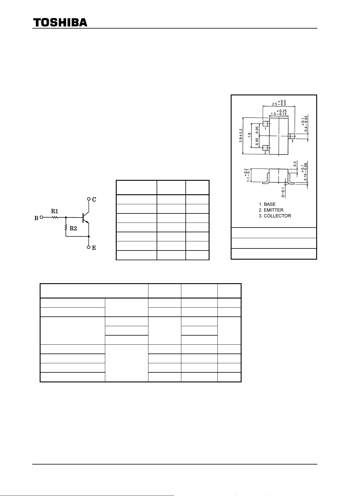
Equivalent Circuit and Bias Resister Values
Unit: mm
Absolute Maximum Ratings
Characteristic Symbol Rating Unit
Collector-base voltage V
Collector-emitter voltage
Emitter-base voltage
Collector current IC 800 mA
Collector power dissipation PC 200 mW
Junction temperature Tj 150 °C
Storage temperature range
Type No. R1 (kΩ) R2 (kΩ)
RN1421 1 1
RN1422 2.2 2.2
RN1423 4.7 4.7
RN1424 10 10
RN1425 0.47 10
RN1426 1 10
RN1427 2.2 10
(Ta = 25°C)
RN1421 to 1427
RN1421 to 1424 10
RN1425, 1426 5
RN1427
RN1421 to 1427
50 V
CBO
V
50 V
CEO
V
EBO
6
T
−55 to 150 °C
stg
S-Mini
JEDEC TO-236MOD
JEITA SC-59
TOSHIBA 2-3F1A
Weight: 12 mg (typ.)
V
Note: Using continuously under heavy loads (e.g. the application of high temperature/current/voltage and the
significant change in temperature, etc.) may cause this product to decrease in the reliability significantly even
if the operating conditions (i.e. operating temperature/current/voltage, etc.) are within the absolute maximum
ratings.
Please design the appropriate reliability upon reviewing the Toshiba Semiconductor Reliability Handbook
(“Handling Precautions”/“Derating Concept and Methods”) and individual reliability data (i.e. reliability test
report and estimated failure rate, etc).
1
2010-08-20

Electrical Characteristics (Ta = 25°C)
RN1421∼RN1427
Characteristic Symbol
I
Collector cut-off
current
Emitter cut-off current
DC current gain
Collector-emitter
saturation voltage
Input voltage (ON)
Input voltage (OFF)
Transition frequency RN1421 to 1427 fT ― V
Collector Output
capacitance
Input resistor
Resistor ratio
RN1421 to 1427
RN1421 3.85 ― 7.14
RN1422 1.75 ― 3.25
RN1423 0.82 ― 1.52
RN1424
RN1425 0.365 ― 0.682
RN1426
RN1427
RN1421 60 ― ―
RN1422 65 ― ―
RN1423 70 ― ―
RN1424 90 ― ―
RN1425 90 ― ―
RN1426 90 ― ―
RN1427
RN1421
RN1422 to 1427
RN1421
RN1422
RN1423
RN1424
RN1425
RN1426
RN1427
RN1421 to 1424
RN1425, 1426
RN1427
RN1421 to 1427 C
RN1421
RN1422
RN1423
RN1424
RN1425
RN1426
RN1427
RN1421 to 1424
RN1425
RN1426 0.09 0.1 0.11
RN1427
CBO
I
CEO
I
EBO
h
FE
V
CE (sat)
V
I (ON)
V
I (OFF)
ob
R1 ― ―
R1/R2 ― ―
Test
Circuit
―
―
― V
―
― V
― V
―
Test Condition Min Typ. Max Unit
V
= 50V, IE = 0 ― ― 100
CB
V
= 50V, IB = 0 ― ― 500
CE
= 10V, IC = 0
V
EB
0.38 ― 0.71
V
= 5V, IC = 0
EB
= 6V, IC = 0 0.378 ― 0.703
V
EB
= 1V, IC = 100mA
CE
I
= 50mA, IB = 2mA
C
= 50mA, IB = 1mA
I
C
= 0.2V, IC = 100mA
CE
= 5V, IC = 0.1mA
CE
= 5V, IC = 20mA ― 300 ―
CE
= 10V, IE = 0,
V
CB
f = 1MHz
0.35 ― 0.65
90 ― ―
―
1.0
1.4
2.0
3.0
0.6
0.7
1.0
0.8
0.4
0.5 1.0
― 7 ―
0.7 1.0 1.3
1.54 2.2 2.86
3.29 4.7 6.11
0.329 0.47 0.61
0.7 1.0 1.3
1.54 2.2 2.86
0.9 1.0 1.1
0.0423 0.047 0.0517
0.2 0.22 0.24
―
―
―
―
―
―
―
―
―
―
7 10 13
0.25
3.5
4.5
6.5
12.0
2.0
2.5
3.0
1.3
0.8
nA
mA
―
V
V
V
MHz
pF
kΩ
―
2
2010-08-20

RN1421∼RN1427
3
2010-08-20
 Loading...