

Page 1
SERVICE TRAINING
1997 G-SERIES
COLOR TELEVISION
POWER SUPPLY
AND SHUTDOWN
TROUBLESHOOTING
GUIDE
Page 2

Contents
POWER SUPPLY CIRCUIT.......................................1
1. OUTLINE OF SYSTEM..................................................................................................................... 2
2. STAND-BY POWER SUPPLY........................................................................................................... 3
3. MAIN POWER SUPPLY.................................................................................................................... 3
4. OUTLINE OF THE CURRENT RESONANT TYPE SUPPLY..................................................... 4
5. FUNDAMENTAL THEORY OF LC SERIES RESONANT CIRCUIT........................................ 4
6. MAIN SUPPLY ACTUAL OPERATION ......................................................................................... 6
7. MAIN POWER SUPPLY TROUBLESHOOTING GUIDE .......................................................... 10
8. SCAN DRIVEN SUPPLY ................................................................................................................. 12
10. SUB POWER SUPPLY.................................................................................................................... 14
11. SUB-POWER SUPPLY TROUBLESHOOTING GUIDE............................................................ 16
SHUT DOWN CIRCUITS.........................................17
1. SUMMARY OF SHUT DOWN CIRCUITS. ................................................................................... 18
2. POWER SHUT DOWN TROUBLESHOOTING GUIDE............................................................ 20
3. +30 Volt Over Voltage Protect. ......................................................................................................... 21
4. +15V Over Voltage Protect. .............................................................................................................. 21
5. +30 V Over Current Protect. ............................................................................................................ 22
6. +15V Over Current Protect. ............................................................................................................. 22
7. -15V Over Current Protect. .............................................................................................................. 23
8. +35V Over Current Protect. ............................................................................................................. 23
9. +/-15V Under Voltage Protect........................................................................................................... 24
10. 200V Under Voltage Protect. .......................................................................................................... 25
11. X-Ray (High Voltage) Protect. ........................................................................................................ 25
12. +125V Over Current Protect. ......................................................................................................... 26
Page 3

POWER SUPPLY CIRCUIT
1
Page 4
1. Outline of system
The block diagram of the power supply is shown in Fig.
1. The N7 chassis consists of the standby power supply
which supplies power to the microcomputer, and the
main power supply which supplies power to the horizontal output and audio output. This chassis also has a
scan driven supply from the flyback which supplies
power to the vertical output, video output, and signal
processing circuts.
The main supply is a current resonating type supply. It
is small in size, highly efficient and reliable.
F801 T801 T802
SR81
Q801
VOLTAGE CONTROL
STR-Z3201
Q843
SW
Q830
SW
D802~D805
Q802
VOLTAGE CONTROL
STR57041
T840
POWER
TRANS.
TPW
1549AZ
D801
D840
F860
R861
Q862
PHOTO COUPLER
F850
Q840
+12V
REG.
T862
CONVERTER
TPW
3332AS
R883
T888
Fig. 1 Power supply block diagram.
CONVERTER
TPW
3330AM
+5V-1 (MICROCOMPUTER)
+12V
+38V
TRANS.
Q430
+26.5V
F851
+15V
TRANS.
LOW VOLTAGE PROTECTOR
-15V
Q840
REG.
Q840
REG.
Q840
REG.
5V-2 (TUNER, COMB, V/C/D etc.)
5V-3 (PIP, ESD/C.C/RGB. SW)
9V-2 (COMB, DSP, CRT-D etc.)
AUDIO OUT
+9V
H.Vcc (V/C/D)
R470
R479
1
Z801
PROTECTOR
H1C1019
3
Q853 Q854
C471
+13(+125V)
R101
+
D471
R7782
O.C.P
Q768
O.C.P
Q759
O.C.P
Q762
R472
R7750
R7765
F.B.T. V.M
+32V (TUNER)
F.B.T.(HEATER)
200V L.V.P. 35V O.C.P
CONVERGENCE
CIRCUIT
F470
R471
2
X-RAY
13
14
16
2
Page 5
2. Stand-by Power Supply
3. Main Power Supply
The stand-by power supply supplies 12Vdc to the relay SR81, 5V to the microprocessor, 5V to the protect
IC, and a reset 5V to the microprocessor. T840 supplies a low AC signal to D840. D840 rectifies the signal and C840 filters it to produce 12Vdc. The 12V is
applied to Q840. Q840 outputs a regulated 5V on pin 5
and supplies a reset 5V at pin 4. Reset occurs when
power is first applied to Q840. The 5V on pin 5 comes
up first while pin 4 stays low. This is the reset condition. After C843 fully charges, pin 4 goes to 5V for
normal operation.
* Troubleshooting Tip:
A loss of the 5 V or reset 5V will prevent the
microprocessor from operating.
F801 D899 C801
Surge
T801
1. Main Power Rectifier Cir cuit
D801 and C810, the rectifier and filter for the main
switching supply, produce 165V. R810 suppresses the
rush current at turn on. SR81 is a relay that turns on the
main supply. The relay is controlled by the microprocessor through the relay drivers: QB30 and Q843.
* Troubleshooting Tip:
Because the microprocessor controls the relay, the
main power supply may not turn on if the microprocessor does not operate properly.
L901
THERMISTOR
+5V-1
Q843
D801
QB30
C810
R810
MICOM
POWER
165V DC
Rectified
output
SR81
C840
T840 D840
C843
Q840
1
2
5
4
3
Fig. 2 Rectifying circuit and standby power
+5V (to MICOM)
Reset
C842
3
Page 6
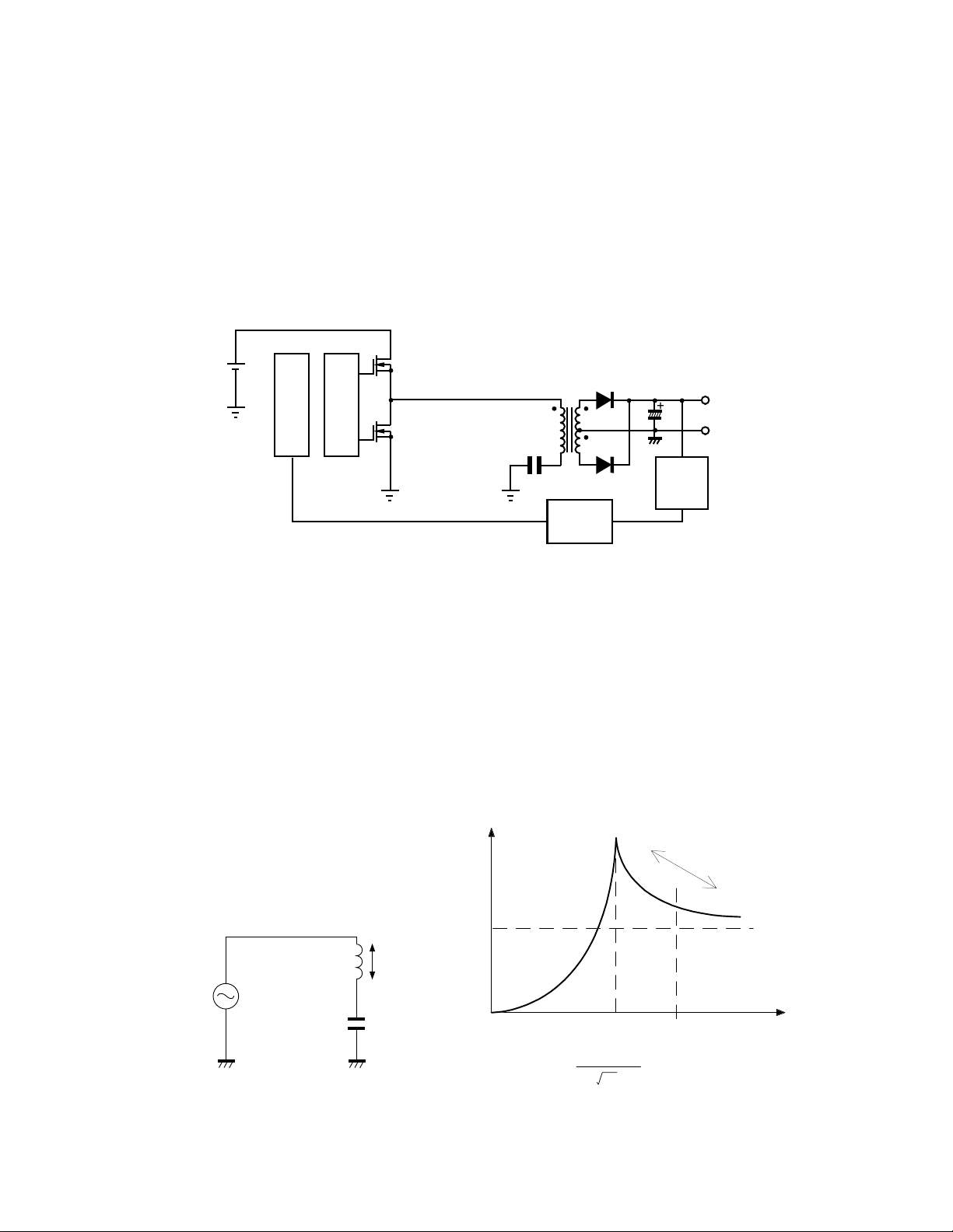
4. Outline of the Current Resonant Type Supply
Fig. 3 shows the block diagram for the current resonant
switch mode power supply. The primary side is an LC
series circuit. It consists of the primary winding of the
transformer and a resonant capacitor in series. Two
power MOS FET’s in a push-pull configuration drive
the primary side of the transformer.
The switching action on the primary side of the transformer produces the main B+ on the secondary side.
The main B+ is regulated by negative feedback. The
main B+ is fed into an error amplifier and outputted to a
photo coupler. The output of the photo coupler is applied to the primary side of the power supply to control
the switching speed.
Oscillator
DRIVE
Fig. 3 Basic configuration
5. Fundamental Theory of LC Series Resonant Circuit
The LC series resonant switch mode power supply is a
frequency regulated power supply oper ating above resonance. When the the load increases on the secondary
side of the transformer, the frequency decreases (operates closer to resonance) and the current increases. Conversely , when the load decreases, the frequency increases
and the current decreases.
B+
ERROR
AMP
PHOTO
COUPLER
VL (v)
Increased Load
Decreased Load
e
Fig. 4 LC series resonant circuit
VL
e
Resonant point
1
f=
LC
2p
Normal
Operating
Frequency
Frequency
Fig. 5 Characteristics
4
Page 7
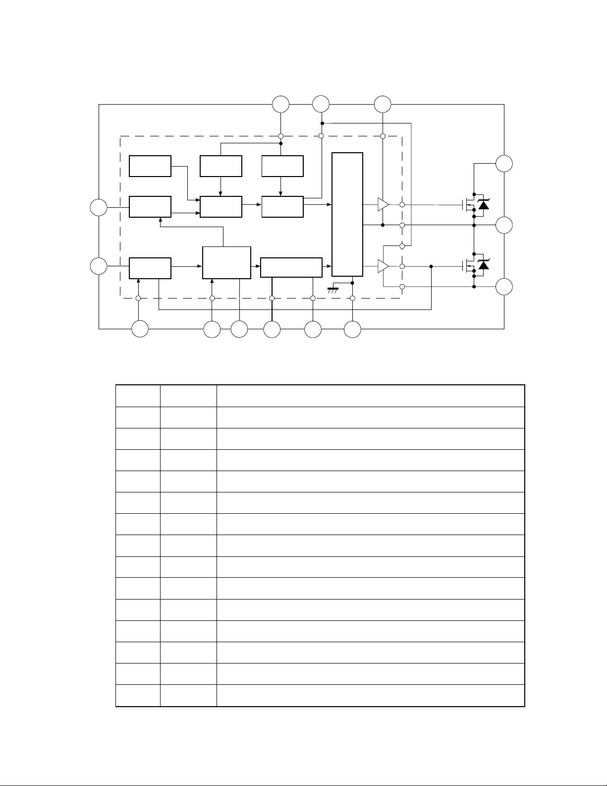
STR-Z415, STR-Z415, and STR-Z4201 Block Diagram
CD
OC
11
Vcc VB
TSD
8
DELAY LATCH REF
OC
7
Css
OVP
OSC
CONTROL
5
CONT
6
Fmax CT
START
DRI Vcc
915
OSC
10
Logic
34
DT GND
2
14
12
1
VIN
OUT
COM
Pin No. Symbol Function
1VIN Half bridge power input
2 Gnd Ground
3 DT Dead time resistor terminal
4 CT Oscillator capacitor terminal
5 CONT Oscillator control terminal
6FMAX Maximum frequency determining resistor terminal
7CSS Soft start capacitor terminal
8 CD Capacitor for delay latch: ON-OFF terminal
9VCC Power source terminal for control section
10 DRI VCC Gate drive power supply output terminal
11 OC Over current detect terminal
12 COM Half bridge GND
14 OUT Half bridge output
15 V
B High side gate drive power source input
Table 2 Pin function
5
Page 8

6. Main Supply Actual operation
Refer to Figure 7 diagram and waveforms.
1. Start-up
When power is applied to the set, a start-up pulse of
16V is applied to pin 9 of IC Q801. At the same time,
the charging of C869 (pin 8) induces a delay to the internal latch circuit to prevent the Over Voltage Protect
(OVP) from engaging, and C866 (pin 7) sets the switching frequency high to reduce the surge current. After
the initial start-up, the circuit operates at its nominal
frequency (70-80 kHz), and the Drive Circuit (see page
9) supplys 17V to pin 9.
2. Output switching element
Two power MOSFETs in push-pull configuration, op-
erate the switching. The on-off timing of each MOSFET is controlled by the logic inside Q801. To avoid
shorting the MOSFET s, they are never turned on at the
same time. Between the time one transistor turns off
and the other turns on, both MOSFETs are of f. This off
time is called dead time, and is determined by
R867(pin3).
3. Basic Oscillation
5.CD terminal (Pin 8) - Latch Delay
The Latch circuit shuts the power supply off (shut-down)
when a fault is detected. Shut-down occurs by detecting
errors from the following:
• Over voltage protection (OVP) circuit
• Thermal shock detection (TSD) circuit
• Over current protection (OCP) circuit
• Loss of and no recovery of Main B+
The charging time of capacitor C869 connected to the
CD terminal (Pin 8) is used to delay the operation of the
latch circuit when power is initially applied. If the unit
goes into shut-down, temporarily remove AC power to
reset the latch circuit.
7.OC terminal (Pin 11) - Over Current Detect
This is to detect over-current in the LC series resonant
circuit.
8.Over voltage protection (OVP) circuit
If the Vcc terminal (Pin 9) exceeds 22V (typical), the
latch circuit is engaged (shutdown) .
The frequency of the internal oscillator is determined
by the charge and discharge of capacitor C862 (pin 4) ,
and is controlled by the feedback into pin 5 through
the Oscillator control block. The oscillator generates a
ramp waveform at Pin 4. The ramp waveform charges
up to 4 V (typical) and discharges to about 2.5 V. The
charging time is the output-on period for one of the
MOSFETs, and the discharging time is the off period
for both MOSFETs (see OSC OUT SIGNAL waveform
of Figure 7). The lowest oscillation frequency is determined by capacitor C862 and resistor R867.
4. Frequency Control
Current flowing out of the CONT terminal (Pin 5) var-
ies the charging time of oscillator capacitor C862, which
in turn, controls the frequency of the Output (Pin 14)
signal. The control current is determined by the
photocoupler. The photocoupler phototransister side current is determined by the feedback current of the photodiode side. The photodiode current is determined by
the error amp inside of Z801, which is monitoring the
+125V source. Thus, the terminal current (CONT) corresponds to the feedback from the +125V output.
9.Thermal shock detection (TSD) circuit
This is to make the Latch circuit operate when the IC's
internal temperature exceeds 150°C.
6
Page 9
Actual Circuit
VIN
(AC)
R810
Q801
C810
C873
D873
R861
Vcc
R862
9
10
D862
T862
D864
R871
#2
V
B
15
#10
D883
MAIN OUTPUT
1
V
TSD
OVP
START
IN
R872
14
12
OUT
COM
C865
C863
D875
C871
R870
7
CD
8
DELAY
LATCH
REF
Logic
11
OC
C869
Css
C866
OC
7
CONT
Q862
OSC
CONTROL
5
Fmax
R864
6
OSC
CT DT
R868
34
D872
GND
2
C862
R867
R866
C867
C868
C874
C870
#3
#4
#5
#12
#11
#14
#13
#15
D884
D855
D886
C884
Q862
C891
R891
Audio
output
R883
Z801
ERROR AMP
Page 10

Voltages On IC801
Using a 100 W light bulb as a Losd
Pin
Voltage Pin Voltage
1 150 Vdc 9 17.7 Vdc
2 0 Vdc 10 7.8 Vdc
3 5.8 Vdc 11 0.9 Vdc
4 2.3 Vdc 12 0 Vdc
5 5.8 Vdc 13 NC
6 5.8 Vdc 14 75 Vdc
7 3.6 Vdc 15 83 Vdc
8 0.4 Vdc
Fig. 8 DC voltages on IC801
Dead time
=4V
CT terminal voltage
OSC output signal
Low side
gate voltage
V
G(L)
High side
gate voltage
V
G(H)
(Pin14)
Push-pull
output voltage
(Pin 14)
Push-pull
output current
ON OFF
OFF ON
=2.5V
=V
IN
terminal voltage (Pin 1)
OV
OA
Figure 7 Terminal waveforms
8
Page 11

Power Supply Troubleshooting Guide.
e
0
Push power button
Check: Sub Power supply, Microprocessor
and Relay drive circuits
Open pin 3&4
of Q862
If 165V and Start up
are present.
Problem is in primary side of power supply.
Recommended circuit checks: IC 801,
Over Current protect, Oscillator, Latch Delay,
LC Resonance, DriveCircuit, and Pre amp.
Open fuse F470
No
B+ to low
Does the relay engage?
Is the B+ at F470
Low or at 0v?
Check start up voltage and 165V on IC 801.
If missing Check F860, D801 SR81 and
surrounding compnonets.
Yes
0V
Main B+ is 140V
150V. Freq. at pin 14
if IC801 is 136KHz.
No
Does the TV go into
Yes
shutdown?
Main B+ reaches 155+ th
to 0v Relay stays on.
Frquency at pin 14 of IC8
is 60Hz
Open F470
Main B+ is below
150V. Freq. at pin 14
if IC801 is above 60Hz.
Open pin 3
of Q862
Problem is in primary side of power supply.
Recommended circuit checks: IC 801,
Over Current protect and Oscillator
Main B+ goes to 155+ then
to 0v Relay stays on. Frquency at
pin 14 of IC801 is 60Hz
Problem in the feedback loop.
Recommended checks: Z801,
and Q862
Problem is in the load.
Main B+ is 140V
150V. Freq. at pin 14
if IC801 is 138KHz.
Main B+ goes to 155+ then
to 0v Relay stays on. Frquency at
pin 14 of IC801 is 60Hz
Short pins 3&4
of Q862
Problem is in primary side of power supply.
Recommended circuit checks: IC 801, and
Oscillator
9
Page 12

7. Main Power Supply Troubleshooting Guide
Poor Regulation:
The Main Power Supply is a looped circuit. In order to
troubleshoot the circuit, the loop must be broken. By
interrupting the feedback portion of the loop, it can be
determined if a problem exists in the primary or secondary side of the supply. Table 3 and 4 shows the switching frequencies of IC801 and the secondary voltages of
the supply with various feedbacks. If the main supply is
not regulating properly , open F470 and check the switching frequency of IC801. Using the tables below, interrupt the feedback. If the frequencies are as shown, the
primary side of the power supply is good. If the frequencies are off, the primary side of the power supply is
bad. Notice that once the feedback is interrupted, the
load has no bearring on the switching frequency.
If the problem is on the primary, C866, R864,
D872,C862, R866,C870 and IC801 should be checked.
If the proplem is on the secondary side, Q862, and Z801
should be checked.
100W light for a load Frequency at pin 14 of
IC801:
Good feedback
Open Feedback: Pins 3 & 4 of Q862
open.
Shorted feedback: Pins 3 & 4 of
Q862 shorted
3K Resistor feedback inplace of pins
3 & 4 of Q862.
No load Frequency at pin 14 of
IC801:
Good feedback
Open Feedback: Pins 3 & 4 of Q862
open.
Shorted feedback: Pins 3 & 4 of
Q862 shorted
3K Resistor feedback inplace of pins
3 & 4 of Q862.
68Khz 124V
60Hhz 140v
138Khz 92V
90Khz 103V
136Khz 140V
60Hhz 160V
138Khz 140V
90Khz 174V
Table 3
Seconday Voltage
at F470:
Seconday Voltage
at F470:
Notes:
Engages Overvoltage
protect on pin 9 of IC801
Notes:
Engages Overvoltage
protect on pin 9 of IC801
Table 4
10
Page 13

No Start-up:
A failure in one of the sub-circuits on the primary side
of the power supply can prevent IC 801 from switching
properly and starting-up. If IC801 is not operating, first
check for 160V on pin 1 of IC801. If this is missing,
check D801,C810,R810 and the relay. If the 160V is
present, refer to Figure 10 and check the following circuits:
Start-up Resistor
Check for a 16V start-up pulse at pin 9. If this is missing, check R68,1 the start-up resistor and D876 (not
shown).
Drive Circuit
Once IC801 starts running, the Drive Circuit supplys
pin 9 with a constant 17V. Therefore, if it fails, IC801
will not run properly. Check D864, R871, and C868.
LC Resonance
If either C870 or T862 opens, no current will flow
through the transformer. All secondary voltages, including the Drive Circuit, will not be present. (See Drive
Circuit)
Latch Delay
To prevent IC801 from going into over-voltage protect
during start-up, the charging of C869 will temporarily
disable the latch. When a DC voltage is applied to the
cap, it acts like a short and it disables the latch. When it's
fully charged, it is an open to DC, and the latch will operate normally. If the capacitor is open, IC801 will not
start-up. Check C869
Over Current Protect
If excessive current flows through the LC Resonance
Circuit, the over-current protect kicks in to protect
IC801. If R866 or R870 fail, it can give a false reading
and shut off the IC801.
Oscillator
C862 is a reference for the oscillator inside IC801. D872
is for protection. A problem here could damage IC801.
Pre-amp Supply
Internal to IC801 are two pre-amps that drive the MOSFETs. When pin 9 has voltage, 9V is supplied from pin
10 to pin 15. This 9V is used to power the internal preamps. Check D873, R862, D862, D875, C873 and C863.
IC801
Check Pins 1,14, and 12 of IC801. If any one of them is
shorted to ground, the IC is bad.
Fig10
VIN
(AC)
R810
Q801
R872
8
CD
11
OC
Css
C866
C869
Latch Delay
C810
TSD
DELAY
OC
7
CONT
Q862
C873
D873
LATCH
OSC
CONTROL
5
R864
Start-up Resistor
R861
Vcc
START
OVP
REF
OSC
6
Fmax
CT
R868
Oscillator
Pre-amp supply
Drive Circuit
R862
D862
V
B
9
10
15
1
V
IN
C865
14
R866
C867
OUT
12
COM
C876
Logic
GND
34
2
DT
C862
R867
D872
Over current protect
D875
C863
D864
C868
C874
R870
LC Resonance
R871
T862
#2
#3
#4
#5
C870
11
Page 14

8. Scan driven supply
The flyback transformer develops a scan driven supply
(T461), shown in Fig. 11. The Flyback supplies 200V
for video output from pin 3, 27V for vertical output from
pin 6, -27V for side DPC from pin 5, and 12V from pin
7. The 12V line produces a regulated 5V and 9V line.
The 5V supplies the tuner and PIP, the 9V supplies the
Video Processing. Resistors and fuses are in each line
for circuit protection
-
27V
+12V
5V
C422
9V
C421 Q421 C422
Q101
+27V
200V
F301
R642
C461
C449
C310 D302
AFC
BLANKING
FAIL SAFE
HEATER
D408
C317
R327
D406
D460
R333
R433
10
FBT
9
5
4
7
6
3
ANODE
FOCUS
SCREEN
+B
C448
Q404
Collector
Fig. 11 Other power supply circuit
2
1
8
ABL
12
Page 15

NOTES
13
Page 16

10. SUB POWER SUPPLY.
and a positive voltage across the Base winding of the transformer increasing the current through the Base of Q1.
The Sub Power Supply is a switching supply. It uses a
Free-Running Oscillator made up of Q802, T888 and
C855. R852 supplies the start-up voltage, and C855 supplies a positive feedback to maintain switching (Fig.14).
The Sup Power Supply supplies a 16V, -16V and 29V to
the Convergence Outputs and the Convergence Digital
Control. This supply also operates as a Main Power Supply in some of the 19” TVs and is similar in operation to
the supplies used in Toshiba’s VCRs and DVD players.
Basic operation:
Refer to Figure 12. RS supplies a start-up voltage to the
base of Q1 turning Q1 on. With Q1 on, current slowly
increases through the primary winding of the transformer.
An electromagnetic field builds while the current increases. This field will induce an electromagnetic field
Primary winding
-
+
Rs
V
I
Q1
-
+
-
+
V
O
Secondary winding
C1
+
Base winding
Feedback.
Eventually, the current through the Collector of Q1 saturates, stops increasing and levels off. At that point, the
electromagnetic field across the Base Winding collapses,
supplies a negative voltage to the Base of Q1, and charges
C1.
The negative voltage on the Base of Q1 turns Q1 off. The
electromagnetic field on the primary collapses, induces
current in the secondary winding, and induces a potential
on the detection winding which continues to hold Base of
Q1 low.
After the electomagnetic field is fully collapsed, C1 discharges truning Q1 on. and this starts the process over again.
The start up voltage in no longer used once the supply starts
switching.
V
CE
Time
0
V
B
0
Ic
0
I
D
0
On
Off
Time
Slant
Slant
V
I
L
P
V
O
L
S
Fig. 12
For stabilization, a negative feedback is supplied to the
Base of Q1. The feedback signal is developed form the
Detection winding, rectified by D856 and controls the
bias of Q1. If the output is too high, the frequency of
Primary winding
Rs
V
I
Dz
D856
Q1 increases resulting in decreased on-time of Q1. This
will then decrease the output voltage. If the output is
too low, the frequency of Q1 decreases. In return, it
increases the on-time of Q1
Secondary winding
Vo
Base winding
Detection winding
Fig. 13
14
Page 17

IC 802
160V
B+
R852
R859
5
C850
C851
Q851
Q852
R857
R860
+
D855
C856
Q850
C845
C849
R846
D848
4
15
R853
D851
R854
C852
L850
3
L851
R847
D849
D847
D850
2
R858
C855
+
R851
C853
1
R850
D856
Page 18

11. Troubleshooting Sub-Power Supply.
Refer to fig 14. To troubleshoot the Sup-Power Supply, it must be isolated from the load. It is necessary to
hookup an external load to the secondary, and use a
Variac. With the Variac set to 40 Vpp and a 100W light
bulb hooked up for a load, the relay has to be shorted to
supply the 40Vpp to the Sub-Power supply.
Dead
First, check the 160 volts Main B+ and Fuse F850.
If the 160V is good and the fuse is open, the transistor
in IC802 maybe shorted. Check for shorts between pins
2,3, and 4 of IC802. If IC802 is good or after replacing
IC 802, make the following checks before restoring the
120V :
* Note: If IC802 is bad, the feedback circuit must be
checked.
Check for switching at pin 2 of IC801.
If the switching is missing, the Start-up circuit maybe
bad. Check R852 for an open, check Q851, Q850 and
Q852 for shorts, and check IC802 for a base emitter
open on Q1. Lastly, check T888 and C855. After restoring the switching, check the feedback: D856, R851,
R820, and C853.
If the switching is good, Check the feedback: D856,
R851,R850, and C853.
Wrong secondary voltage or improper regulation
A loss of feedback will cause the secondary voltage to
increase and can damage IC802 resulting in no power.
Check the following components of the Secondary voltages are to low:
R853 and R854 the Over Current protect resistors.
Q850, Q851, and Q852 the Soft Start transistors and
surrounding circuit.
C855 Oscillator Capacitor.
16
Page 19

SHUT DOWN CIRCUITS
17 JRS 12-97
Page 20

1. Summary of Shut down circuits.
Figure 14 is a block diagram of the eleven shut down
circuits. When any of the shut down conditions occur,
the latch in Z801 holds the power relay off as long as the
set is plugged in. Neither the front panel power switch,
nor the remote power switch will restore power to the
set. The front panel power LED will blink at approximately 1/2 second intervals. T o reset the shut down condition, the AC main power cord must be unplugged.
Plug the AC cord back in. While listening carefully for
the click of the power relay activating, turn the power
on. If the power relay clicks on, then immediately off,
and the power LED starts blinking, then a shut down
condition has occured.
If the relay doesn't energize at all, check the AC input
circuits, fuse F801, and the standby power supply.
If the relay clicks on and the power LED remains steady
on, the set is not in shut down.
When the set does go into shut down, the problem becomes how to determine which conditioned caused it.
X-ray Protect.
The X-ray protect is connected to pin 13 of Z801. Z801
compares this voltage to the reference voltage on pin 11
(aproximately 25 volts). If the voltage on pin 13 rises to
a value GREATER than pin 11, shut down occurs and
all power goes away, except the standby supply.
A peak response meter connected at pin 13 of Z801,
while power is applied to the set, will capture a voltage
greater than the reference voltage, indicating excessive
High Voltage.
+125V Over Current Protect.
The peak hold meter is connected across resistor R470,
and NOT referenced to ground to monitor for a momentary increase in voltage. The normal voltage across R470
is about 0.4Volts. An increase in current will cause the
voltage across R470 to increase. When Z801 detects
this voltage increase, it puts the set into shut down.
Peak Response Meter.
Each shut down circuit has a "Trigger Voltage", which
will cause shut down. The trigger voltage lasts for just a
brief moment before the power supply shuts off. A PeakResponse Meter is required to troubleshoot the shut
down circuits. A peak response meter measures and
holds the highest voltage that occurs at a test point.
Nine circuits are connected to pin 14 of Z801. Each of
these circuits operate in a similar manner. Normally , all
"triggers" are approximately zero volts. When an abnormal condition occurs, the appropriate shut down circuit triggers a "high" to pin 14 of Z801. Z801 sets and
holds pin 16 low (0 volts). This causes relay SR81 to de
energize, dropping all power in the TV, except the
standby power. This means the trigger voltage also goes
away. There is now no means to determine which circuit caused the shut down. The only way to reset Z801
is to pull the AC plug.
T o determine which cicuit triggered the shut down, connect the peak response meter to each shut down circuit
Trigger monitor point in turn, while applying power to
the set. Any voltage at a monitor point above
aproximately 2 volts is a clear indication that the circuit
being monitored is in shut down, narrowing the search
for the actual fault.
18 JRS 12-97
Page 21

Figure 14. Summary of Shutdown circuits.
19 JRS 12-97
Page 22

2. Power shut down troubleshooting guide.
20 JRS 12-97
Page 23

3. +30 Volt Over Voltage Protect.
When the supply voltage goes beyond the zener votage,
the zener diode conducts and delivers a voltage to the
anode of D 863. This passes through the diode switch,
D863, to pin 14 of Z801, and shut down takes place.
Normal voltage at the monitor point is about 0. A voltage of about 2.5V or greater will result in shut down.
Figure 15. +30V Over Voltage Protect.
4. +15V Over Voltage Protect.
The +15V over voltage protect operates in a similar fashion as the +30V over votage protect.
Figure 16. +15V Over Voltage Protect.
21 JRS 12-97
Page 24

5. +30 V Over Current Protect.
Resistor R 7782 is the Sensing Resistor. It is a very
small value. It can cause intermittent shut down problems.
The current flow to the convergence circuits flow through
this resistor. T oo much current will cause an increase in
the voltage across the resistor. Transistor Q768 is biased just below cutoff. A slight increase in voltage across
R 7782 will turn on Q768. The collector then goes to
about 30V. This is the monitor point for shut down.
The normal collector voltage is Zero.
This trigger voltage will turn on Q758. It's collector
will go low, to about 0V. This, in turn, causes transistor
Q757 to turn off. Q757's collector rises to about 5V,
causing shut down to occur.
Figure 17. +30V Over Current Protect.
6. +15V Over Current Protect.
The +15V over current protect operates in a similar fashion as the +30V over current protect.
Figure 18. +15V Over Current Protect.
22 JRS 12-97
Page 25

7. -15V Over Current Protect.
The -15V over current protect operates in a manner similar to the +15V over current protec circuit.
Figure 19. -15V Over Current Protect.
8. +35V Over Current Protect.
A +35V source is developed at the cathode of Diode
D302. The load current is carried through current sense
resistor R370. If the load current exceeds a certain limit,
the voltage drop across R370 increases and turns on transistor Q370.
When Q370 turns on, the collector will go high, towards
the +35V supply. This is the monitor point for shut down.
The Zener diode D370 goes into breakdown, and a high
voltage is delivered to pin 14 of Z801.
Figure 20. +35V Over Current Protect.
23 JRS 12-97
Page 26

9. +/-15V Under Voltage Protect.
The two circuits work independantly, and do not affect
each other.
The +15V turns on transistor Q853. This causes the
collector of Q853 to stay low, about 0V. If the +15V
goes low, Q853 will turn off, and the collector will go
high, to about 5. This will pass through the diode switch,
D 866, and shut down will take place.
The -15V turns on transistor Q854. This causes the collector of Q854 to go to about -15V. If the -15V goes
low, Q854 will turn of f, the collector will go towards the
12V supply. Thios will pass through the diode switch,
D867, and shut down will take place.
Figure 21. +/-15V Under Voltage Protect.
24 JRS 12-97
Page 27

10. 200V Under Voltage Protect.
The flyback transformer T 461 produces about 200V at
the cathode of D406. This is dropped to about 6.8 V on
the base of Q340. Under normal operation, Q340 is
turned on. This keeps Q341 turned off. The collector
of Q341 is about 0 V.
When the 200V drops to about 160V, Q340 turns off,
and Q341 will turn on. When Q 341 turns on, its collector voltage will go to about 6 V, sending the high to pin
14 of Z801, resulting in shut down.
Figure 22. 200V Under Voltage Protect.
11. X-Ray (High Voltage) Protect.
The cathode of D885 is about +40V. This developes a
+25V reference to pin 11 of Z801. The cathode of D471
developes a nominal voltage of +22V to pin 13 of Z801.
As long as the X-Ray monitor point voltage is LESS
than the reference voltage at pin 11 of Z801, operation
is normal.
If the cathode voltage of D471 increases, excessive High
Voltage may also be occuring.
When D471 cathode voltage goes GREATER than the
reference voltage, shut down occurs.
Figure 23. X-Ray (High Voltage) Protect.
25 JRS 12-97
Page 28

12. +125V Over Current Protect.
The current sensing resistor, R470, is in series with the
+125V supply.
During normal operation, the voltage drop across R470
is approximately 0.5V. The turn on surge voltage drop
is approximately 1.5V.
If the supply current exceeds a certain level, the increased
voltage drop across R470 causes shut down to take place.
Figure 24. +125V Over Current Protect.
If the voltage across R470 exceeds about 1.8V , shut down
will occur.
26 JRS 12-97
 Loading...