

Page 1

NTDPJTV008
TOSHIBA
TECHNICAL TRAINING MANUAL
N7SS CHASSIS
PROJECTION TELEVISION
TOSHIBA AMERICA CONSUMER PRODUCTS, INC.
NATIONAL SERVICE DIVISION
TRAINING DEPARTMENT
1420-B TOSHIBA DRIVE
LEBANON, TENNESSEE 37087
PHONE: (615) 449-2360
FAX: (615) 444-7520
www.toshiba.com/tacp
TP71G90
©1997
Page 2

CONTENTS
SECTION I
OUTLINE...........................1-1
1.OUTLINE....................................................1-2
2.SPECIFICATIONS 37 KEYS...................1-3
3.TP71G90 SERIES DIFFERENCES.........1-4
PC Board Layout.......................................1-5
TP71G90 Block Diagram..........................1-6
SECTION II
AUDIO CIRCUIT................2-1
1.GENERAL...................................................2-2
2.FLOW OF SIGNAL...................................2-2
Audio Circuit Block Diagram...................2-3
3.DESCRIPTION OF CIRCUITS...............2-4
3-1.IMA Module (MVUS34S/MVUS34B)........2-4
3-2.A. PRO Circuit............................................2-4
3-3.A/V Selector Circuit...................................2-4
QV01(TA8851CN) Block Diagram...........2-5
3-4.Surround-sound Circuit.............................2-6
3-5.Audio Output Circuit..................................2-6
SECTION III
TUNER/IMA CIRCUIT....3-1
1.CIRCUIT BLOCK.....................................3-2
1-1.Outline........................................................3-2
1-2.RF SW.........................................................3-3
1-3.TUNER........................................................3-3
1-4.TIF for PIP.................................................3-4
1-5.IMA.............................................................3-4
1-6.CATV System AUTO MODE Decision......3-5
2.IF/RF CIRCUIT
TROUBLESHOOTING.............................3-6
2-1.No Picture of VHF/UHF
(Main Screen).............................................3-6
2-2.No Picture of VHF/UHF
(PIP Screen)................................................3-7
SECTION IV
CHANNEL SELECTION
2.HARDWARE COMPONENT...................4-2
3.MICROCOMPUTER.................................4-3
3-1.Microcomputer Terminal Function..........4-4
3-2.Microcomputer Terminal Name
and Operation Logic..................................4-5
4.E2PROM (QA02)........................................4-6
5.ON SCREEN FUNCTION........................4-6
6.SYSTEM BLOCK DIAGRAM.................4-7
7.LOCAL KEY
DETECTION METHOD...........................4-8
8.REMOTE CONTROL CODE
ASSIGNMENT CUSTOM
COES ARE 40-BFH...................................4-9
9.ENTERING TO SERVICE MODE.......4-11
10.TEST SIGNAL SELECTION.................4-11
11.SERVICE ADJUSTMENT......................4-11
12.FAILURE DIAGNOSIS
PROCEDURE.....................................................4-12
12-1.Contens to be Confirmed by Customer......4-12
12-4.Understanding Self Diagnosis
Function Indication..................................4-13
13.TROUBLE SHOOTING CHART..........4-14
13-1.TV does not turn ON................................4-15
14-2.No Acception of Key-IN...........................4-15
14-3.No Picture (Snow Noise)...........................4-15
14-4.Memory Circuit Check............................4-16
14-5.No Indication on Screen...........................4-16
SECTION V
VIDEO CIRCUIT..............5-1
1.A/V SELECTOR CIRCUIT......................5-2
1-1.General.......................................................5-2
1-2.Speifications...............................................5-2
1-3.Operation of the Circuit.............................5-3
2.VIDEO PROCESSING CIRCUIT...........5-4
2-1.General.......................................................5-4
2-2.V/C/D IC (Q501).........................................5-4
3.CRT OUTPUT CIRCUIT..........................5-7
3-1.General.......................................................5-7
3-2.Output Circuit............................................5-7
3-3.Blue Extension Circuit...............................5-8
CIRCUIT............................4-1
1.OUTLINE OF CHANNEL
SELECTION CIRCUIT SYSTEM...........4-2
SECTION VI
YCS/DUAL CIRCUIT.......6-1
i
Page 3

1.GENERAL...................................................6-2
2.OPERATION PRINCIPLE.......................6-2
2-1.DUAL Block................................................6-2
2-2.YCS (3-dimension YCS Separator)
Block...........................................................6-2
2-3.Memory Selector Block.............................6-2
3.CIRCUIT OPERATION............................6-2
3-1.DUAL Section.............................................6-2
3-2.YCS Section................................................6-3
4.TERMINAL DESCRIPTION...................6-3
4-1.PY01............................................................6-3
4-2.PZ01............................................................6-3
4-3.QZ01 (TC90A28F).....................................6-4
5.YCS TROUBLESHOOTING....................6-6
6.BLOCK DIAGRAM...................................6-7
VERTICAL OUTPUT CIR-
CUIT...................................9-1
1.OUTLINE....................................................9-2
1-1.Theory of Operation..................................9-2
2.V OUTPUT CIRCUIT...............................9-3
2-1.Actual Circuit.............................................9-3
2-2.Sawtooth Waveform Generation..............9-3
2-3.Vertical Output...........................................9-4
2-4.Vertical Linearity
Characteristic Correction.........................9-6
2-5.Centering Circuit.......................................9-6
3.PROTECTION CIRCUIT FOR
VERTICAL DEFLECTION STOP..........9-7
3-1.+35V Over Current Protection Circuit.....9-8
SECTION VII
DOUBLE-SPEED CIRCUIT
(UPCON)..............................7-1
1.GENERAL...................................................7-2
2.CIRCUIT OPERATION............................7-2
2-1.Signal Flow.................................................7-2
2-2.Clock/Sync Signal......................................7-3
2-3.I2C BUS.......................................................7-3
3.BLOCK DIAGRAM...................................7-4
4.PIN ASSIGNMENT....................................7-5
5TERMINAL DESCRIPTION AND
TROUBLESHOOTING.............................7-8
SECTION VIII
SYNC SEPARATION CIRCUIT &
HORIZONTAL OSCILLATION CIR-
CUIT.........................................
1.OUTLINE....................................................8-2
2.SYNC SEPARATION CIRCUIT
AND 32 fH OSCILLATOR.......................8-4
2-1.Theory of Operation..................................8-4
3.HORIZONTAL AND VERTICAL
OSCILLATION CIRCUIT.......................8-5
3-1.IC (LA7860) Operation.............................8-6
2-2.Horizontal Phase Shift Circuit................8-14
8-1
SECTION IX
SECTION X
HORIZONTAL
DEFLECTION CIRCUIT....10-1
1.OUTLINE..................................................10-2
2.HIGH VOLTAGE CIRCUIT..................10-2
2-1.General.....................................................10-3
2-2.X-ray Protection Circuit..........................10-3
2-3.200V Low Voltage Protection Circuit.....10-4
3.DEFLECTION CIRCUIT.......................10-5
3-1.General.....................................................10-6
3-2.S-character Capacitor Switching............10-6
3-3.Horizontal Stop Protection circuit.........10-6
3-4.CRT Protection Circuit............................10-9
SECTION XI
DYNAMIC FOCUS CIRCUIT
11-1
1.OUTLINE..................................................11-2
SECTION XII
DIGITAL CONVERGENCE
CIRCUIT..........................12-1
1.OUTLINE..................................................12-2
2.CIRCUIT DESCRIPTION......................12-2
2-1.Configuration...........................................12-2
2-2.Circuit Operation.....................................12-2
3.PICTURE ADJUSTMENT......................12-4
3-1.Change of Memory (E2PROM)...............12-4
3-2.Service Mode............................................12-4
4.ADJUSTING PICTURE DIMENSION
ii
Page 4

(GREEN PICTURE) ................................. 12-5
5. KEY FUNCTION OF
REMOTE CONTROL UNIT .................. 12-6
6. TROUBLESHOOTING ........................... 12-6
6-1. Adjusting Procedure in Replacing CR T ......12-6
6-2. Adjusting Procedure in Replacing
Conver gence Unit/Main Def. ...................12-6
7 . DIGITAL CONVERGENCE CIRCUIT .. 12-7
7-1. Outline ...................................................... 12-7
7-2. Screen Adjustment....................................12-7
7-3. Adjustment Procedures when Requesting
Convergence Adjustment...........................12-8
8 . CONVERGENCE OUTPUT CIRCUIT .12-11
8-1. Outline ................................................... 12-11
8-2. Circuit Description................................ 12-11
9. CONVERGENCE
TROUBLESHOOTING CHART ......... 12-13
SECTION XIII
OPTICAL SECTION ......13-1
1. NECK COMPONENTS ...........................13-2
1-1. Outline of Components around Neck
of the Projection Tube ..............................13-2
1-2. Theory of Operation ................................13-2
1-3. Projection Tube ........................................13-2
2 . FUNCTION OF KEY COMPONENTS . . 13-3
2-1. Outline ...................................................... 13-3
2-2. Theory of Operation ................................13-3
2-3. ????...........................................................13-3
2-4. Optical Coupling Effect ........................... 13-4
2-5. Lens ...........................................................13-5
2-6. Focus Adjustment .....................................13-6
4. POWER-2.................................................14-11
4-1. Outline of Current Resonant
T ype Supply ........................................... 14-11
4-2. Fundamental Theory ............................ 14-12
4-3. Actual Circuit ........................................ 14-13
4-4. Main Functions of the Control Unit ...... 14-15
5. PROTECT FUNCTION ......................... 14-17
6. TROUBLESHOOTING ......................... 14-18
SECTION XV
CLOSED CAPTION/EDS
CIRCUIT ..........................15-1
1. OUTLINE .................................................. 15-2
2. DATA TRANSMISSION FORMAT....... 15-2
3. DISPLAY FORMAT ................................. 15-2
4. CIRCUIT OPERATION.......................... 15-2
SECTION XIV
POWER SUPPLY
CIRCUIT ..........................14-1
1. OUTLINE .................................................. 14-2
1-1. ST ANDBY Power Supply.........................14-2
1-2. Power-1 .....................................................14-2
1-3. Power-2 .....................................................14-2
1-4. Protect Function .......................................14-2
1-5. Power Supply Line Connection
Diagram....................................................14-3
2. STANDBY POWER SUPPLY ................. 14-4
3. POWER-1 ................................................... 14-4
3-1. Block Diagram ......................................... 14-4
3-2. STR-6811A Pins and Peripheral
Circuit Operation.....................................14-6
iii
Page 5

SECTION I
OUTLINE
1-1
Page 6
1. OUTLINE
(1) Family common chassis;
TP61G90 (different from TP71G90 in size,
data is different from that in contents.)
TW65G80 (WIDE MODEL)
(2) EDTV Engineering;
• Progressive Scan
• Exclusive CRT (long-neck type)—improving
Linearity.
• Color-lens employed in R/G (flare reduction )
• New 3D-YCS (common with domestic model,
32DW77)
• Protection sheet (coating) low-refection
• PIP picture-quality is the same as the main
picture because of using DUAL-UNIT used.
(3) General feature including adjustment are
common with TP50G60.
(4) WIDE specifications of TW65G80 are common
with TW40F80/TW56F80. (Fig. 1-1)
SCR EEN
SIZE
TH EATE R
WIDE
DUAL
STANDARD
1
TH EATE R W ID E
2
DUAL 9 SCREEN SEARCH
Fig. 1-1
3
321
FU LL
1-2
Page 7
2. SPECIFICATIONS 37 KEYS
Table 1-1
Chassis
Model
CRT
CRT Source
Remote H/U
RMT keys
GENER
PIP
V-Chip
Dolby Surr
Surround
SAP
Cyclone
SBS
SOUND
Audio(W)
Woofer
Rear
Comb-Filter
DOF
Scan-Modul
VCC
Black-Expan
Color-D, E
Pic-Prefer
Color-Temp
PICTURE
Flesh-Tone
Nois-Reduce
Wide Modes
Progressive
Rori-Resolve
Fav-Channel
Ch-label
3-Language
Clock
Ch-Lock/Off
C. Caption
EDS
New-OSD
OTHERS
Multi-Conv
D/A Switch
D/W POP
Multi-Window
S/Sight
S-video In
AV-In/Out
Gold Plated(E2)
Color Differ
Front-Term
A(Var)-OUT
AC-3 A.OUT
2RF-Ter m
SPK-Term
TERMINAL
PIP Audio
C-Ch-Input
E / Jack
S /S-Jack
RGB (F/R)
IR-B & 750
Adapter
Rod-Antenna
SPK-Box
ACCE
EZ RMT
Protective
Cabinet
TP61G90
7
Hitachi
Intell
37key
2-TN
¾
¾
·
·
¾
·
28W
¾
¾
3D-Y/C
·
·
·
·
·
·
·
·
—
¾
·
560DI
·
·
·
·
·
·
¾
·
¾
·
¾
¾
¾
1+1
1+2/1
·
·
·
·
¾
·
¾
¾
·
¾
¾
¾
¾
¾
¾
¾
¾
·
TP61F80
TP61G60
7
Hitachi
UnIB/L
37key
2-TN
¾
¾
·
·
¾
·
28W
¾
¾
2LDIG
·
·
·
·
·
·
·
·
·
¾
¾
800
·
·
·
·
·
·
·
·
¾
·
¾
¾
¾
1+1
1+2/1
·
·
·
·
¾
·
¾
¾
·
¾
¾
¾
¾
¾
¾
¾
¾
OPTION
TP61F80
TP55G90
7
TSB
Intell
37key
2-TN
¾
¾
·
·
¾
·
28W
¾
¾
2LDIG
·
·
·
·
·
·
·
·
·
¾
¾
800
·
·
·
·
·
·
·
·
¾
·
¾
¾
¾
1+1
1+2/1
·
·
·
·
¾
·
¾
¾
·
¾
¾
¾
¾
¾
¾
¾
¾
·
TP55F80
TP55G65
7
Hitachi
UnIB/L
37key
2-TN
¾
¾
·
·
¾
·
28W
¾
¾
2LDIG
·
·
·
·
·
·
·
·
·
¾
¾
800
·
·
·
·
·
·
·
·
¾
·
¾
¾
¾
1+1
1+2/1
·
·
·
·
¾
·
¾
¾
·
¾
¾
¾
¾
¾
¾
¾
¾
OPTION
TP55F80
C - Chassis
TP55G60
7
TSB
UnIB/L
37key
2-TN
¾
¾
·
·
¾
·
28W
¾
¾
2LDIG
·
·
·
·
·
·
·
·
·
¾
¾
800
·
·
·
·
·
·
·
·
¾
·
¾
¾
¾
1+1
1+2/1
·
·
·
·
¾
·
¾
¾
·
¾
¾
¾
¾
¾
¾
¾
¾
OPTION
TP55F80
TP71G90
7
Hitachi
Intell
37key
2-TN
¾
¾
·
·
¾
·
28W
¾
¾
3D-Y/C
·
·
·
·
·
·
·
·
—
¾
·
560DI
·
·
·
·
·
·
¾
·
¾
·
¾
¾
¾
1+1
1+2/1
·
·
·
·
¾
·
¾
¾
·
¾
¾
¾
¾
¾
¾
¾
¾
·
NEW
TW65G80
7
Hitachi
Intell
37key
2-TN
¾
¾
·
·
¾
·
28W
¾
¾
3D-Y/C
·
·
·
·
·
·
·
·
—
·
·
560DI
·
·
·
·
·
·
¾
·
¾
·
·
·
¾
1+1
1+2/1
·
·
·
·
¾
·
¾
¾
·
¾
¾
¾
¾
¾
¾
¾
*
¾
·
NEW
TP50G90
7
Hitachi
Intell
37key
2-TN
¾
¾
·
·
¾
·
28W
¾
¾
2LDIG
¾
·
·
·
·
·
·
·
·
¾
¾
800
·
·
·
·
·
·
·
·
¾
·
¾
¾
¾
1+1
1+2/1
·
·
·
·
¾
·
¾
¾
·
¾
¾
¾
¾
¾
¾
¾
¾
·
TP50F60
TP50G60
7
Hitachi
UnIB/L
37key
2-TN
¾
¾
·
·
¾
·
28W
¾
¾
2LDIG
¾
·
·
·
·
·
·
·
·
¾
¾
800
·
·
·
·
·
·
·
·
¾
·
¾
¾
¾
1+1
1+2/1
·
·
·
·
¾
·
¾
¾
¾
¾
¾
¾
¾
¾
¾
¾
¾
OPTION
TP50F60
TP50G50
7
Hitachi
UnIv
38key
1-TN
¾
¾
¾
·
¾
·
28W
¾
¾
2LDIG
¾
¾
·
·
·
·
·
·
·
¾
¾
800
·
·
·
·
·
·
·
¾
¾
¾
¾
¾
¾
1
2/1
¾
¾
¾
·
¾
¾
¾
¾
¾
¾
¾
¾
¾
¾
¾
¾
¾
OPTION
TP50F50
TP48G10
7
Hitachi
UnIv
38key
1-TN
¾
¾
¾
·
¾
·
28W
¾
¾
2LDIG
¾
¾
·
·
·
·
·
·
·
¾
¾
800
·
·
·
·
·
·
·
¾
¾
¾
¾
¾
¾
1
2/1
¾
¾
¾
·
¾
¾
¾
¾
¾
¾
¾
¾
¾
¾
¾
¾
¾
OPTION
TP48F50
1-3
Page 8
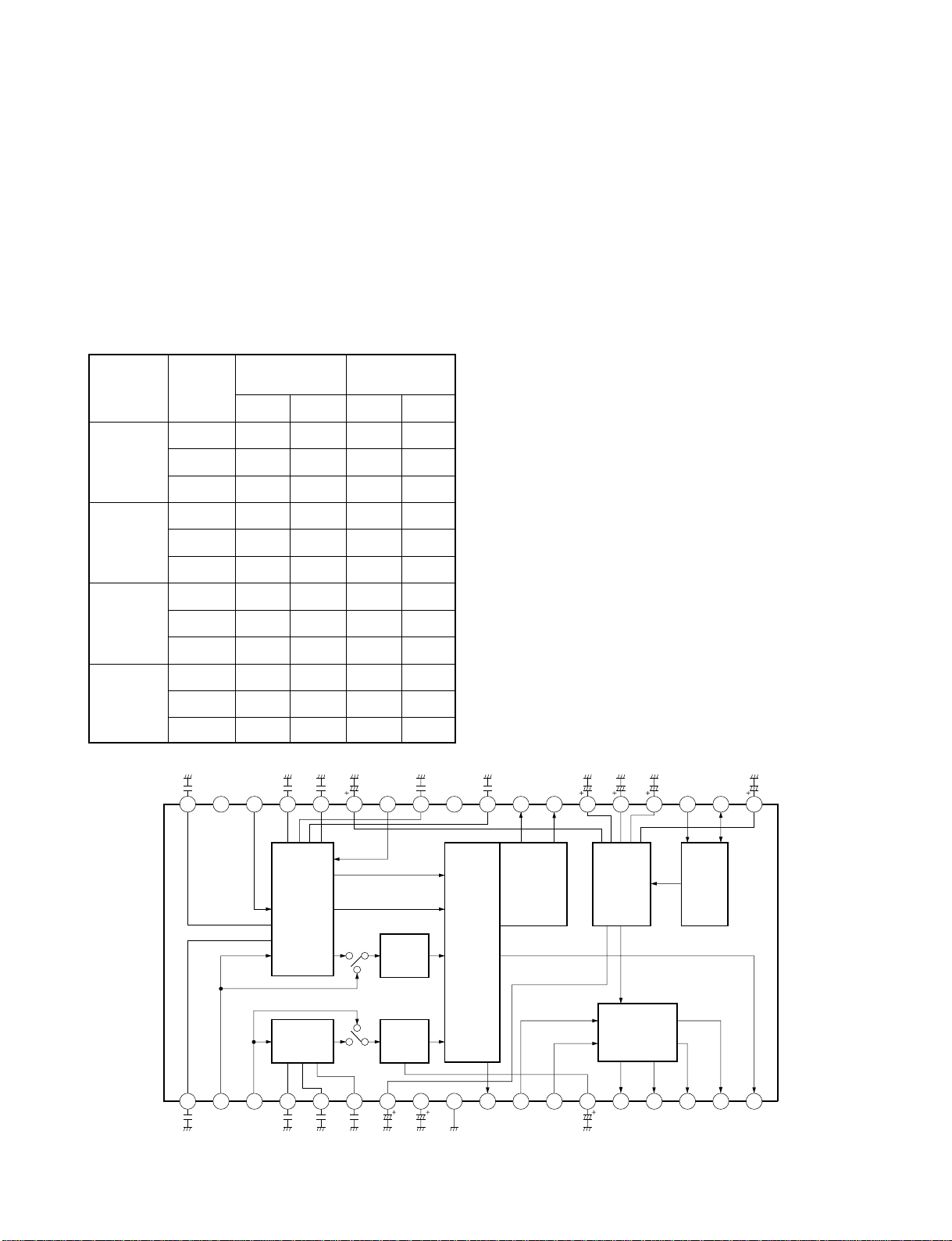
3. TP71G90 SERIES DIFFERENCES
Table 1-2
SIGNAL
DEF
WAC
WAC POWER
D.F.&S.CRRE
V-SHIFT
ABL
WAC-UNIT
L518, L519, L520
GJ21. GJ22. GJ23
GJ28
PW01A. PW02A
QQ03. QQ03A. QQ03B
CQ05. CQ06
RQ03
QA01
QA02(MEMORY)
SR41 (RELAY)
C411
C491
C493
Q490
Q491
R498
D444
C318
Q304
Q305
R321
R322
R323
R324
R218
R220
R219
C220
Q220
TP71G90/TP61G90
DEL.
DEL.
JP
DEL.
DEL.
DEL.
DEL.
DEL.
8700CSN-113
8K
DEL.
DEL.
DEL.
DEL.
DEL.
DEL.
DEL.
DEL.
DEL.
DEL.
DEL.
DEL.
DEL.
DEL.
DEL.
1/6W10KG
1/6W9.1KG
DEL.
DEL.
DEL.
TW65G80
PB6348
TEM2028K
DEL.
JP
8P-BB
PQ09RF11.H/S
50V10 m16V47m
1/6W4.7K
8700CSN-115
16K
DJ12D1
400V0.027
400V0.15
MO.1
2SC1740S,Q
RN1203
4.7K
1SS133
MO.1
2SA1020Y
RN1203
2R120
2R120
1/6W1K
1/6W5.6K
1/6W12KG
1/6W11KG
1/6W27KG
M0.1
RN1204
SIGNAL
DEF
CONV-OUT
POWER
A/V
CRT-FRONT
OSD
DIGI-CONV
YCS/DUAL
UP-CON
WAC
PB7289
PB7300
PB7290
PB7301
PB7291
PB7396
PB7302
PB7292
PB7303
PB7293
PB7294
PB7571
PB7572
PB7295
PB7333
PB7296
PB7397
PB7304
PB7297
PB7299
PB6348
TP71G90
O
O
O
O
O
O
O
O
O
O
TP61G90
O
O
O
O
O
O
O
O
O
O
O
TW65G80
O
O
O
O
O
O
O
O
O
O
O
Table 1-3
UNIT
23706637
23706652
23706638
23706653
23706639
23706850
23706655
23706640
23706656
23706641
23706642
23781086
23781091
23706648
23706684
23706649
23706851
23706657
23706650
23706651
23705379
1-4
BOARD
23536159
23536169
23536160
23536170
23536161
23536229
23536171
23536162
23536172
23536163
23536164
23526335
23536336
23536165
23536192
23536166
23536230
23536174
23536167
23536168
23535595
BASE
23545340
23545340
23545341
23545341
23545342
23545342
23545342
23545343
23545343
23545344
23545345
23545345
23545296
23545346
23545346
23545347
23545347
23545347
23545348
23545349
23484617B
BASE UNIT
PB7189
PB7342
PB5454ZBW
SPECIFICATION
E2096K459
E2096K469
E2096K460
E2096K470
E2096K461
E2097K003
E2096K471
E2096K462
E2096K472
E2096K463
E2096K464
E2097K041
E2097K042
E2096K465
E2097K001
S2096K466
S2096K004
S2096K473
S2096K467
S2096K468
S9095K112
Page 9
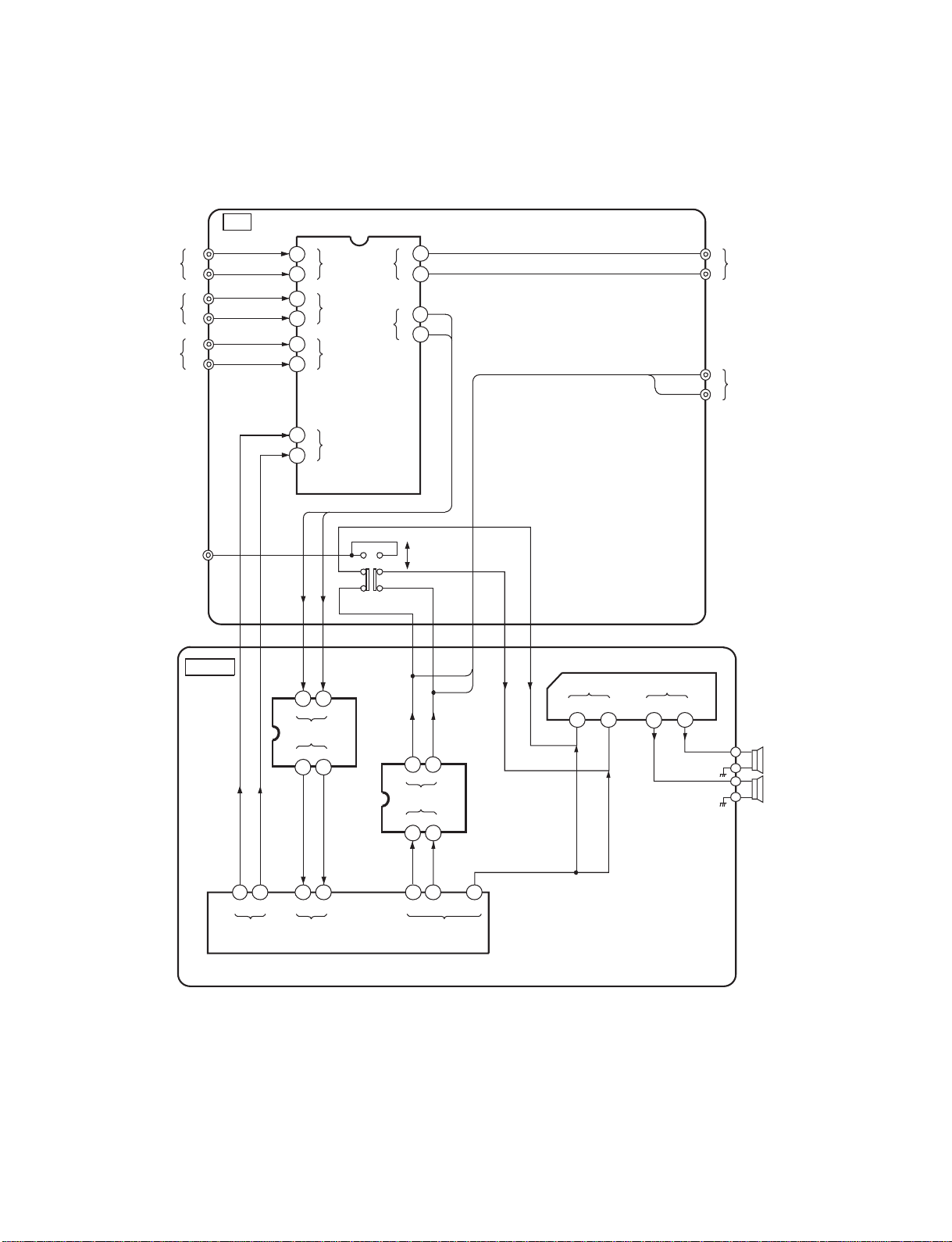
4. TP71G90 (TW65G80) CHASSIS LAYOUT
U901
SIGNAL
FRONT-IN
FRONT-CONT
UX01
UY01
YCS/DUAL
UP - CON
(PIP)
2nd
TUN
(TIF)
UM01
New-OSD
UX02
WAC
ONLY
UV01
A/V
TW65G80
SVM
CRT-D/GCRT-D/B CRT-D/R
DEF-OUT
DPC
POW1
V-
H-
OUT
OUT
U401
DEF
U701
CONV-OUT
UH01
D-CONV
Fig. 1-2
Fo
PAC
1-5
POW2
STANDBY
U801
POWER
Page 10
CENTER-IN
ON OFF
2
:I BUS ELEM ENT
SPEAKER
AUDIO AMP
ANT1
OUT
ANT2
VIDEO1 S.V.L.R
V ID E O 2 V .L .R
/D V D C r.C b
VIDEO3 S.V.L.R
MONITO R-OUT
AUDIO VAR I-OUT
2HD, 2VD
TUNER IM A
TIF
DEF IC
PIP-V
TV-V, L, R
D-CONV
CONV-OUT
V . D R IV E
SURROUND IC
SPK-O UT
L/R
AV SW ITCH
VYC
YCS
DUAL
Y. I. Q
SW
C. C. IC
OSD IC
TO DY (SUB YOKE)
MAIN-Y
MAIN-C
RGB
RGB
V. O UT
WAC
2HD.2VD
VCD IC
YIQ
WIDE
ONLY
UP-CON
SVM
RGB
HD, VD
2Y IQ
MICRO
PRO CESSOR
DEF. H. V. DRIVE
A C 120V
H. D. FOCUS
DEF. OUT
FOCUS
PACK
H. V. O UT
FBT
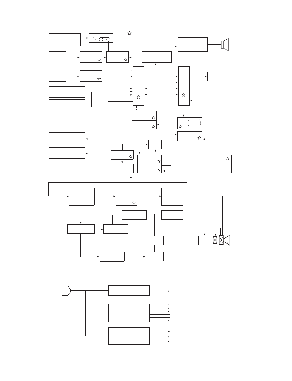
Fig. 1-3 TP71G90 block diagram
POW -STANBY
POW ER1
POW ER2
V.D.FOCUS
SCREEN
FOCUS
CRT-D
5V -1
148V (H -O U T)/120V (S V M )/32V (TU N )
3 5 V (V -O U T )
15V
11V/9V -1/9V -2/9V -3/9V-4(9V-4,W ID E O NLY )
7V-1/5V -3/5V -A /5V -D
7V-2/5V-2/HEATER
35V(A U D IO )
21V(CONV)/5V(D-CONV)
-21V(CO NV)/5V(D -CO NV)
CRT.
Fig. 1-4
1-6
Page 11

SECTION II
AUDIO CIRCUIT
2-1
Page 12

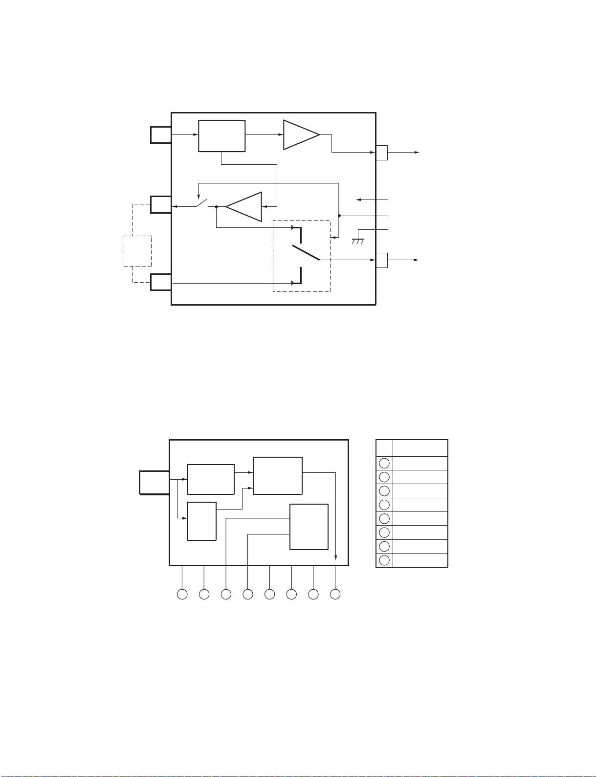
1. GENERAL
The audio signal processing circuit consists of an input
selector IC (QV01 = TA8851CN), a master IMA (H002
= MVUS34S, MVUS34B) modules, a Surround-soundsound IC (QD01 = TA8173AP) and a VARIABLE-AUDIO-AMP (QS101 = M5218AP) and an audio output IC
(Q601 = LA4282). The audio output of TP71G90 is 14W
+14W, which is based on SBS (SUB BASS SYSTEM) as
a basic specification. When the double window feature
is selected, the left-hand screen sound is output.
2. FLOW OF SIGNAL
Fig. 2-1 shows a block diagram of the audio circuit of
TP71G90.
• TV detection output
Pins 12 (R-OUT) and 14 (L-OUT) of IMA module
H002.
• A/V selector IC input
Pins 6 (R-IN) and 4 (L-IN) of QV01 (TA8851CN).
This A/V selector IC receives the audio signals from
TV, E1, E2 and E3.
• A/V selector IC output
Pins 39 (R-OUT) and 41 (L-OUT) of QV01.
The signal here is regarded as 1.
• Surround-sound-sound IC input
Pins 16 (R-IN) and 14 (L-IN) of QD01.
• Surround-sound-sound IC output
Pins 9 (R-OUT) and 11 (L-OUT) of QD01.
• IMA module A. PRO input
Pins 16 (R-IN) and 18 (L-IN) of H002.
• IMA module A. PRO output
Pins 26 (R-OUT), 24 (L-OUT) and 22 (W-OUT) of
H002.
• VARIABLE-AUDIO-AMP input
Pins 3 (R-IN) and 5 (L-IN) of QS101.
• VARIABLE-AUDIO-AMP output
Pins 1 (R-OUT) and 7 (L-OUT) of QS101.
• Audio output IC input
Pins 2 (R-IN) and 5 (L-IN) of Q601.
• Audio output IC output
Pins 11 (R-OUT) and 7 (L-OUT) of Q601.
• SPK output
2-2
Page 13
E1
T
E2
E3
R
L
R
L
R
L
A/V
10
8
49
51
22
20
6
4
R
L
R
L
R
L
R
L
QV01
TA 8851C N
MON-out
E1
E2
SPK-out
E3
TV
R
L
R
L
43
45
39
41
R
MONITOR
out
L
VARIABLE
R
AUDIO OUTPU
L
TER M IN A L
CENTER
AUDIO
IN
SIG NAL
QD01
TA 8173AP
16
14
R L
In
Out
R L
9 11
14
12
R L
TV out
16 18
R L
In
H 002 M VUS34S O R M VU S34B
ON
OFF
1
7
R L
Out
In
R L
3
5
26
24
R
L
Out
Q S 101
M 5218AP
22
W
Q 601 LA4282
In
R L
2
5
Out
R L
7
11
SPK
L
R
Fig. 2-1 Audio circuit block diagram
2-3
Page 14
3. DESCRIPTION OF CIRCUITS
3-2. A. PRO Circuit
3-1. IMA Module (MVUS34S/MVUS34B)
3-1-1. MTS Circuit
This has the following functions.
• Discriminating STEREO and SAP
• MATRIX output selection for STEREO and SAP
Table 2-1 shows the output MATRIX in each broadcast
mode.
Table 2-1 Multi-channel MATRIX
R
R
R
Multi-channel
display
Stereo
SAP
O
O
O
Feed
MONO
STEREO
Mode
selection
STEREO
SAP
MONO
STEREO
SAP
MONO
Speaker output
L
MONO
MONO
MONO
MONO
MONO
MONO
L
L
L + R
L + R
The self-made A. PRO TA1217AN is used. This has the
following functions.
• VOLUME CONTROL
• TONE CONTROL (BASS , TREBLE, BALANCE)
• SBS LEVEL CONTROL
• SBS ON/OFF
All these functions are controlled by I2C BUS sent from
a microcomputer.
Fig. 2-2 shows the block diagram of A. PRO.
3-3. A/V Selector Circuit
(1) Input source selected with QV01
Signals from TV, E1, E2 and E3
Fig. 2-3 shows the internal block diagram of QV01
(TA8851CN). Select always the master (left-hand screen)
signal for the SPK-OUT (pins 39 and 41) signal.
MONO +
SAP
STEREO
+ SAP
STEREO
SAP
MONO
STEREO
SAP
MONO
Address
SW
36
35 34
MONO
SAP
MONO
SAP
L + R
L in
MONO
SAP
MONO
L
R
SAP
L + R
32 31 30 29
33
TONE
CONTROL
LPF LEVEL
O
O
O
O
O
O
sre
O
O
O
R in Vcc
28
VOLUME BALANCE
LEVEL
27
R out L out
26 25
vol bass
24
23 22 21
D/A
CONV
I/O
bal
SCL SDA
I C
2
20
OLev
19
1 2
C in W in
3
4
5 6 7
9
WLev
8
Rip
fil
10 11
W out
GND
12 13
P1 P2
Fig. 2-2 TA1217AN block diagram
2-4
14
15 16 17 18
P3 P4
P5 P6
C out
Page 15
VT1
VB1/Y121
VT2
VB2/Y122
VE1
VE2
VE3
YE1
YE2
YE3
CE1
CE2
CE3
TV1 R
E2 R
E1 R
E3 R
TV1 L
E2 L
E1 L
E3 L
5
50
2
53
7
13
19
9
15
21
11
17
23
6
49
3
52
10
16
22
4
51
1
54
8
14
20
DAC
DAC
DAC
DAC
DAC
ST1
ST2
SE1
SE2
SY1
SY2
SC1
SC2
SR1
SR2
SL1
SL2
6dB
AMP
6dB
AMP
6dB
AMP
6dB
AMP
Speaker audio SW
SV1
SV2
PIP output SW
SRT
PIP output
SW
SLT
RB2, LB2,
VE1, VE2, VE3
6dB
AMP
6dB
AMP
Clamp
SOY1
SOC1
Clamp
SOY2
SOC2
I/O
2
I C
DAC
Mute
VO1
46
1
2
fcl1
47
YI11
48
YO1
44
CO1
42
CI1
40
VO2
36
fcl2
37
YI12
38
YO2
34
CO2
32
CI2
30
SPK-out R
39
SPK-out L
41
MON-out R
43
MON-out L
45
33
35
O3
31
I/O1
28
I/O2
29
SDA
26
SCL
27
Mute
25
12
18
Vcc GND1 GND2
24
Fig. 2-3 QV01 (TA8851CN) block dia gram
2-5
Page 16
3-4. Surround-sound Circuit
Surround-sound processing is performed by TA8173AP.
Fig. 2-4 shows the internal block diagram of TA8173AP.
LF1 PS1 PS2 PS3 PS4 LF2 VCC
3
2
5
6
4
7
8
LPF 2 (R-L)
R IN
16
BUF
L IN
14
BUF
REF
15
REF
Fig. 2-4 Surround process IC TA8173AP block diagram
3-5. Audio Output Circuit
This uses LA4282, and permits output of 14W + 14W.
Fig. 2-5 shows the block diagram.
PHASE
SHIFT
t 2 (R-L)
+
R
-
+
L
1
GND
LPF
+
LPF
LPF
N D
BUF
BUF
REF
D/N SW
13
R OUT=R+
9
R LPF
10
L OUT=L - t 2 (R-L)
11
12
L LPF
t 2 (R-L)
1
2
Input (1)
Feed back (1)
30k
300
ch1
+
Ripple
Filter
3 4
Ripple filter
Input side GND
+
5
Input (2)
ch2
30k
300
6
7
Output (2)
Feed back (2)
Muting
Ckt.
8
External mute
Fig. 2-5 LA4282 block diagram
Thermal
shut-down
Over-voltage
Vcc
9
Output side GND (2)
11
10
Output (1)
Power supply
12
Output side GND (1)
2-6
Page 17
Does sound go on
in video 1 mode?
NG
OK
Does VHF/UHF sound
go on?
NG
Go to Fig. 2-8.
Check the output
waveform at QV01,
pins 39 and 40.
OK
Check the output
waveform at QD01,
pins 9 and 11.
OK
NG
NG
Check the voltage of 9V
DC at QV01, pin 18.
OK
Check the input waveform
at QV01, pins 8 and 10.
OK
Replace QV01.
Check the voltage of 9V
DC at QD01, pin 8.
OK
Check the input waveform
at QD01, pins 14 and 16.
OK
Replace QD01.
NG
NG
NG
NG
Check the power supply circuit.
Check the QV01 peripheral
circuit.
Check the power supply circuit.
Check the QD01 peripheral
circuit.
Check the output
waveform at H002,
pins 24 and 26.
OK
Check the output
waveform at QS101
pins 1 and 7.
NG
Check the voltage of 9V
DC at H002, pin 27.
OK
Check the input waveform
at H002, pins 16 and 18.
OK
Replace H002.
Fig. 2-6
2-7
NG
NG
Check the power supply circuit.
Check the H002 peripheral
circuit.
Page 18
Check the output
waveformat at H002,
pins 24 and 26.
OK
Check the output
waveform at QS101,
pins 1 and 7.
OK
Check the output
waveform at Q601,
pins 7 and 11.
OK
Check C609, C610
W661 and W662.
NG
Check the voltage of
9V DC at QS101, pins 8.
OK
Check the input waveform
at QS101, pins 3 and 5.
OK
Replace QS101.
Check the voltage of 34V
DC at Q601, pin 10.
OK
Check the input waveform
at Q601, pins 2 and 5.
OK
Replace Q601.
NG
NG
NG
NG
Check the power supply circuit.
Check the QS101 peripheral
circuit.
Check the power supply circuit.
Check the Q601
peripheral circuit.
Does VHF/UHF sound go on?
NG
Check the output
waveform at H002,
pins 12 and 14.
NG
Fig. 2-7
Check the voltege of
9V DC at H002, pin 4.
OK
Replace H002.
Fig. 2-8
2-8
NG
Check the power supply circuit.
Page 19

SECTION III
TUNER/IMA CIRCUIT
3-1
Page 20
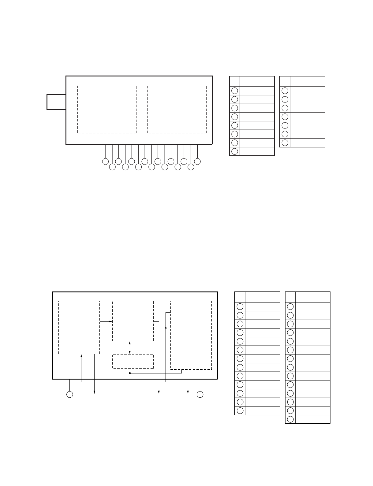
1. CIRCUIT BLOCK
1-1. Outline
A TV signal input to ANT1 is provided to HY01 (TIF for
PIP) and H001 (main tuner) through a splitter H003(RFSW) is a new RF-SWITCH with an isolation amplifir added
to the divider output to improve local interference between
the main and the sub tuner.
H003 controls, signal selection for ANT1 or ANT2 to be
supplied to H001 (main tuner) according to the IMA MODULE-DAC-OUT 2.
H001 is of an international standardtype tuner and supplies the signals (Video: 45.75 MHz Audio: 41.25 MHz)
in the IF (Intermediate-Frequency) band to the IMA.
ANT1
OUT
H003
RF
SW
HY01
TIF for PIP
EL924L2
The TV signal input to ANT1 is always provided to HY01
(TIF for PIP) as the splitter output and demodulated to a
video signal for PIP.
H002 (IMA) is module containing the IF circuit consisting of a split carrier PLL synchronizing detection system
and multiplex sound decorder and audio processer.
But in the MPX section, former HIC type is replaced by a
module consisting of MPX-IC, I2C bus control and sound
multiplex data exclusive memory IC, thereby affering a
non alignment in the replacement service.
AFT2
PIP VIDEO
VIDEO L/R
H002
ANT2
H001
SW Tr
TUNER
ELA12L
Q151/Q152
Fig. 3-1 Block diagram
IMA (IF/MPX/A,PRO)
MVUS34B
DAC
OUT2
AFT1
3-2
Page 21
1-2. RF SW
C able
Box
ANT1
OUT
ANT2
DIO DE
SW
H003 Model : RSU134 (SN : 23344412)
D ivider
AM P
RELAY
SW
AM P
Fig. 3-2 Block diagram
PIP TIF
9V
S W C o n tro l(A N T 1 : O P E N )
G N D (A N T 2 : 9 V )
TUNER
1-3. TUNER
H001 Model : ELA12L (SN : 23321223)
ANT in
Pin
No.
UHF
AM P
VHF
AM P
2
1
3
MIX
OSC
45
PLL
6
7
8
1
2
3
4
5
6
7
8
Nam e
AGC
ADD RESS
CLOCK
DATA
9V
5V
32V
IF
Fig. 3-3 Block diagram
Pin2 (ADDRESS) in the main tuner is open and controlled by microcomputer
RECEPTION BAND AREA VHF LOW : CH~2B
VHF HIGH : CHC~LL
UHF : CHMM~69
3-3
Page 22
1-4. TIF for PIP
TIF for PIP with no-sound is newly developed.
HY01 Model : EL924L2 (SN : 23321263)
Pin
No.
ANT in
TUNER
1
2
IF
In te r c a rrie r P L L
3
5
4
6
7
9
8
10
13
11
12
15
14
1
2
3
4
5
6
7
8
Fig. 3-4
The Pin6 (ADDRESS) in the PIP TIF is GND, and controlled by the microcomputer.
RECEPTION BAND AREA VHF LOW : CH2~B
VHF HIGH : CHC~LL
UHF : CHMM~69
Nam e
NC
32V
CLOCK
DATA
NC
ADDRESS
5V
RF AGC
Pin
No.
9
10
11
12
13
14
15
Nam e
9V
NC
GND
AFT
NC
GND
VIDEO
1-5. IMA
H002 Model : MVUS34B (SN : 23148280)
Split carrier
PLL
IF
IF in BUS R/Lin
1
VIDEO TV R/L L/R/Wout
Multiplex
sound
decord
Memory
Audio
procceser
Fig. 3-5
27
Pin
No.
1
2
3
4
5
6
7
8
9
10
11
12
13
Name
GND
IF in
NC
9V
RF AGC
AFC
VIDEO
IF AGC
MPX out
SAP VCO
ADDRESS
TV R
DAC out 1
Pin
No.
14
15
16
17
18
19
20
21
22
23
24
25
26
27
Name
TV L
DAC out 2
Rin
Cin
Lin
GND
CLOCK
DATA
W out
C out
L out
GND
R out
9V
3-4
Page 23
The Exclusive IC memory that memories adjustment values for I2C bus control sound multiplex IC is built in module, and this eliminates readjustment of the sound multiplex recontrol in the module-replacement.
1-6. CATV System AUTO MODE Decision
In the initial state (shipping and AC ON), the channel selection is carried out in the STD mode and the pull in
operation is carried out by the sync and AFT signals. By
this time, offset value from STD mode is memorized.
Two memories, memory 1 and memory 2, are required for
the channels 5, 6 and the channels other than the channels
5, 6. A cable mode is decided by this offset values memorized and the start frequency of next channel selection is
determined. The offset value is updated each time. The
criterion of the decision and the start frequency are shown
in tables 3-1 and 3-2.
Table 3-1 Channels other than the channels 5, 6c h
Offset values
+0.75 ~ +2.5 MHz
-0.75 ~ +0.75 MHz
-2.25 ~ -0.75 MHz
Table 3-2 Channels 5, 6
Offset values
+1.375 ~ +2.5 MHz
+0.5 ~ +1.375 MHz
-0.5 ~ +0.5 MHz
-2.25 ~ -0.5 MHz
Decision
NEW
STD/IRC
HRC
Decision
5, 6ch IRC
5, 6ch HRC
5, 6ch STD
5, 6ch OTHER
Start frequency
fo +1.75 MHz
fo
fo -1.25 MHz
Start Frequency
fo +2.00 MHz
fo +0.75 MHz
fo
fo -1.00 MHz
3-5
Page 24
2. IF/RF CIRCUIT TROUBLESHOOTING
2-1. No Picture of VHF/UHF (Main Screen)
No picture of VHF/UHF
250mV
(p-p)
H period
Check waveform
at pin 7 of H002.
AC 1.0V(p-p)
NG
Check power voltage at pin 4
of H002 is 9V.
OK
Check waveform
at pin 2 of H002.
NG
OK
NG
OK
Check waveform at
pin(EP) of A/V connecter.
AC 1.0V(p-p)
NG
Investigate power circuit.
Replace H002.
OK
Check A/V board.
Check pattern from
pin 7 of H002 to pin(EP.)
Check waveform at pins SDA
SCL(BUS line) of H001.
OK
Check power voltage of H001.
9V
5V
32V
OK
Replace H001
NG
NG
Investingate Bus line.
Investingate power circuit.
Fig. 3-6
3-6
Page 25
2-2. No Picture of VHF/UHF (PIP Screen)
No picture of VHF/UHF
Check waveform
at pin 15 of HY01.
AC 1.0V(p-p)
NG
Check waveform at pins 3
and 4 (Bus line) of HY01.
OK
Check power voltage of HY01.
9V
5V
32V
OK
Replace HY01.
OK
NG
NG
Check waveform at
pin(EL) of A/V connecter.
AC 1.0V(p-p)
Investigate Bus line.
Investingate power circuit.
Fig. 3-7
OK
NG
Check A/V board.
Check pattern from
pin 15 of HY01 to pin(EL.)
3-7
Page 26

This page is not printed.
3-8
Page 27

SECTION IV
CHANNEL SELECTION CIRCUIT
4-1
Page 28

1. OUTLINE OF CHANNEL
SELECTION CIRCUIT SYSTEM
The channel selection circuit in the N7SS chassis employs
a bus system which performs a central control by connecting a channel selection microcomputer to a control
IC in each circuit block through control lines called a bus.
In the bus system which controls each IC, the I2C bus
system (two line bus system) developed by Philips Co.
Ltd. in the Netherlands has been employed.
The ICs controlled by the I2C bus system are : IC for audio signal processing (QN06), IC for V/C/D signal processing (Q501), IC for A/V switching (QV01), IC for non
volatile memory (QA02), Main and sub U/V tuners (H001,
HY01), IC for deflection distortion correction (Q302), IC
for PIP signal processing (QY04), IC for closed caption
control, A.PRO, I/O expander, JFORC, digital convergence, 3D YCS, SLC, V/C/D for PIP.
2. HARDWARE COMPONENT
(4) External Input Switching SW IC
(TOSHIBA TA8851CN)
• Performs source switching for main and sub pictures.
• Switches total 4 systems of TV and video 3 inputs.
(5) Memory IC
(MICROCHIP 24LC08BI/P)
• Memorizes the user last status for video and audio adjustment values, volume, external status,
etc.
• Memorizes the parameters which determines the
picture formation and distortion correction of the
white balance data, deflection yoke data, etc.
(6) U/V Tuner Control IC
(MATSUSHITA EL466L)
• Controls U/V channel selection frequency
(1) Channel Selection Microprocessor
The 8-bit single chip microprocessor (TLCS-870
series) is applied. The outline of the microprocessor
is shown below.
• Production type name: TMPA8700CSN-113
• ROM: 60 k X 8 bits
• RAM: 2 k X 8 bits
• Pa ckage : SDIP42-P-600
• OTP built-in: TMPA8700PSN
(2) Audio System Control IC
(TOSHIBA TA1217AN)
• Controls balance, sound quality adjustment such
as high and low sounds and volume.
• Switc hes the SURROUND ON/OFF
• Switches SBS and perfor m level adjustment
• Switches audio mute
(3) Video System Control IC
(TOSHIBA TA1259N)
• Controls video system such as CONTRAST,
BRIGHTNESS, COLOR, TINT, SHARPNESS.
• Adjusts SUB COLOR, SUB BRIGHTNESS, SUB
TINT and other video system parameter.
• Switches the modes for PICTURE PREFERENCE, COLOR TEMPERATURE.
(7) 7DPC Unit Control IC
(TOSHIBA TA1241N)
• Performs pin-cushion distortion correction
(8) PIP Control IC
(TOSHIBA TC90A17F)
• Performs sub picture ON/OFF, LOCATE, STILL,
etc.
(9) C/C Control Microprocessor
(MITUBISHI M37274MX)
• Performs CLOSED CAPTION mode switching
(10) Digital Convergence Control IC
• Performs digital convergence correction control
• Memorizes convergence data
(11) 3D YCS Control IC
(TOSHIBA TC90A28F)
• Performs 3D YCS ON/OFF switc hing (at PIP ON)
• Performs 3D YCS operation control
4-2
Page 29
(12) Video IC for PIP
(TOSHIBA TA1270F)
• Adjusts the video system parameter of SUB
COLOR, SUB BRIGHTNESS, SUB TINT, etc.
for PIP
(13) JFORC (183E2550AF02)
• Controls picture compression/extension in vertical direction
• Controls picture vertical position
(14) SLC (TOSHIBA TC90A04AF)
• Converts in order
3. MICROCOMPUTER
Microcomputer TMP A8700CSN-113 has 60k byte of R OM
capacity and equipped with OSD function inside.
The specification is as follow.
• Type name : TMPA8700CSN-113
• ROM : 60k byte
• RAM : 2k byte
• Processing speed : 0.5 ms (at 8 MHz with
shortest command)
• Package : 42 pin shrink DIP
•I2C-BUS : two channels
• PWM : 14 bits X 1, 7 bits X 9
• ADC : 8 bits X 6 (Successive
comparison system,
Conversion time 20ms)
This microcomputer performs functions of AD converter,
reception of U/V TV.
I2C device controls through I2C bus. (Timing chart : See
Fig. 4-1)
• LED uses big current por t for output only.
• For clock oscillation, 8 MHz ceramic oscillator is used.
•I2C has two channels. One is for E2PROM only.
• Self diagnosis function which utilizes ACK function
of I2C is equipped
• Function indication is added to service mode.
• Remote control operation is equipped, and the control
by set no touch is possible. (Bus connector in the conventional bus chassis is deleted.)
• Substantial self diagnosis function
(1) B/W composite video signal generating function
(micom inside)
(2) Generating function of audio signal equivalent to
1 kHz (micom inside)
(3) Detecting function of power protection circuit op-
eration
(4) Detecting function of abnormality in IIC bus line
(5) Functions of LED blink indication and OSD indica-
tion
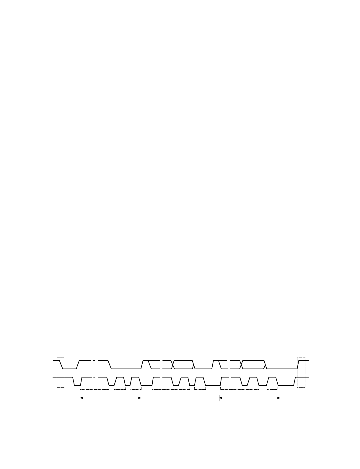
SDA
SCL
Start
condition
1 - 7
Address
8
R/W
Approx.180 µS
9
Ack Data
1 - 7
Fig. 4-1
4-3
9
8
Ack
1 - 7
Some device may have no data,
or may have data with several
bytes continuing.
8
DATA Ack
9
Stop
condition
Page 30
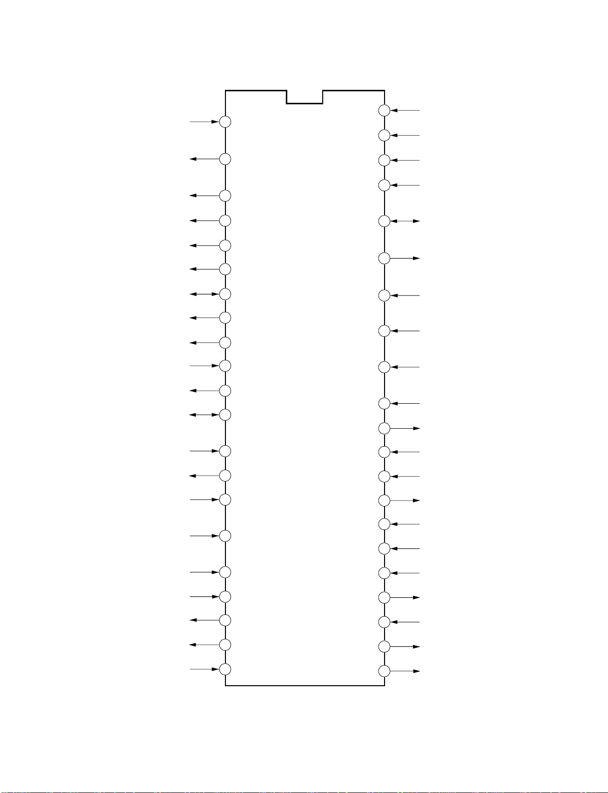
3-1. Microcomputer Terminal Function
VSS
JRESET
RMT OUT
Lor H
ACTIVE=H, NORMAL=L
ACTIVE=H, NORMAL=L
POWER ON=H, OFF=L
POWER ON=Hz, OFF=L
POWER ON=H, OFF=L
ACTIVE=L, NORMAL=H
AC PULSE INPUT
2
I C - BUS CLOCK
ACTIVE=L, NOT DVD MODE=H
SUB TUNER S
MUTE
SPK MUTE
POWER2
POWER1
LED
PIP RESET
ACP
SCLO
SDAO
2
I C - BUS DATA
SYNC VCD
MAIN SYNC
DVD
AFT2
- CURVE
10
12
13
14
15
11
42
1
<P33>
41
∗
<P40>
∗
2
<P41>
∗
3
<P42>
∗
4
<P43>
∗
5
<P44>
∗
6
<P45>
∗
7
<P46>
∗
8
<P47>
∗
9
<P50>
∗
<P51>
∗
<P52>
∗
<P53>
∗
<P54>
∗
<P55>
∗
<P32>
<P35>
<P34>
<P31>
<P30>
<P20> - -
40
∗
39
38
∗
∗
37
∗
36
∗
35
34
33
32
31
30
29
VDD
PIP VIDEO
PIP SYNC
GND
SDA1
2
I C - BUS DATA
SCL1
2
I C - BUS CLOCK
AV SYNC
SUB SYNC
RMT
VD
RST
NORMAL=H, ACTIVE=L
XOUT
SYSTEM CLOCK
XIN
SYSTEM CLOCK
GND
TEST PORT
OSCO
MAIN TUNER S
NORMAL=L
NORMAL=L
AFT1
- CURVE
KEY - A
ADC 0~5V
KEY - B
ADC 0~5V
SGV
SGA
VSS
16
17
18
19
20
21
<P56>
∗
<P60>
∗
<P61>
∗
<P62>
∗
<P63>
∗
<P57>
∗
Fig. 4-2
4-4
28
<P71> -
27
<P70> -
26
<P67>
∗
25
<P66>
∗
24
<P65>
∗
23
<P64>
∗
22
: TRISTATE I/O
∗
: SYNC OPEN DRAIN OUTPUT
−
OSCI
VSYNC
PIP VSYNC
GND
DATA
OSD IC CONTROL
BUSY
OSD IC CONTROL
CS
OSD IC CONTROL
CLK
OSD IC CONTROL
Page 31

3-2. Microcomputer Terminal Name and Operation Logic
Table 4-1
Pin
No.
1
2
3
4
5
6
7
8
9
10
11
12
13
14
15
16
17
18
19
20
21
22
23
24
25
26
27
28
29
30
31
32
33
34
35
36
37
38
39
40
41
42
Terminal
Name
VSS
JRESET
REM OUT
MUTE
SPK MUTE
POWER2
POWER1
LED
PIP RST
ACP
SCL0
SDA0
SYNC VCD
DVD
AFT2
AFT1
KEY-A
KEY-B
SGV
SGA
OSD RESET
OSD CLK
OSD CS
OSD BUSY
OSD DATA
VSS
VSYNC
OSCI
OSCO
GND
XIN
XOUT
RST
VD
RMT
AV SYNC
SCL1
SDA1
GND
PIP SYNC
PIP VIDEO
VDD
I/O
O
P4CR (OCH)
O
P4CR (OCH)
O
P4CR (OCH)
O
P4CR (OCH)
O
P4CR (OCH)
O
P4CR (OCH)
I/O
P4CR (OCH)
O
P4CR (OCH)
O
P4CR (OCH)
I
P5CR1 (09H)
O
P5CR2 (FAEH)
I
P5CR2 (FAEH)
I
P5CR1 (09H)
O
P5CR1 (09H)
I
P5CR1 (09H)
I
P5CR1 (09H)
O
O
O
O
O
P5CR1 (09H)
O
O
I
O
I
I
I
O
I
I
O
I
I
I
I
O
I/O
I
I
I
I
P6CR (0DH)
P6CR (0DH)
P6CR (0DH)
P6CR (0DH)
P6CR (0DH)
P6CR (0DH)
P6CR (0DH)
P6CR (0DH)
P7 (07H)
P7 (07H)
—
—
—
—
P2 (02H)
P3 (03H)
P3 (03H)
P3 (03H)
P3 (03H)
—
—
—
—
D0=1
D1=1
D2=1
D3=1
D4=1
D5=0/1
D6=1
D7=1
D0=1
D1=0
D2=0
D3=0
D4=0
D5=0
D6=0
D0=0/1
D1=0/1
D2=1
D3=1
D7=1
D4=1
D5=1
D6=0
D7=1
D0=1
D1=1
D2=1
D3=0
—
—
—
—
D0=1
D0=0
D1=1
D4=1
D5=1
—
—
—
—
Functions & Logic
Microcomputer GND, 0V connection
Active = H, Normal = L
RMT output
Sound mute output, Mute = H, Normal = L
Speaker mute, Mute = H, Noraml = L
DEF power control, POW ON = H, POW OFF = L
Power supply control, POW ON: Hz, POW OFF: L
LED control, ON: H, Reset: L
PIP reset, ON: H, OFF: L
AC pulse input
Non volatile memory I2C-bus clock, rising sync
Non volatile memory I2C bus data
Main sync, negative logic
DVD mode switching, L: at color difference input, H: normal
Sub tuner AFT, S character input
Main tuner AFT, S character input
Local key A control, 0 ~5V
Local key B control, 0 ~ 5V
Test patter n output, Noraml: L
Test audio output, Nor mal:L Active:1 kHz squarewave
OSD IC reset, Normal: H, Reset: L
OSD IC control clock, CLK frequency: approx. 20 kHz
ODS IC control CS, Active: L
OSD IC busy, Nor mal: L, Busy: H
OSD IC control data
0V
PIP vertical sync pulse detection for V-CHIP
Not used.
Not used.
Micorcomputer shipping test
System clock
oscillation connection terminal (8 Hz)
Hard reset terminal, negative logic
Vertical sync pulse detection
Remote control signal detection , Negative logic
RF sync judgement, Sync: H, No sync: L
I2C bus clock, rising sync
I2C bus data
Slicer ground, 0V connection
V-CHIP
terminal
Microcomputer power supply 5V
4-5
Page 32

4. E2PROM (QA02)
E2PROM (non-volatile memory) has function which, in
spite of power-off, memorizes the such condition as channel selecting data, last memory status, user control and
digital processor data. The capacity of E2PROM is 8k bits.
EEPROM (QA02)
1
A0
Device address
GND
A1
A2
Vss
2
3
4
Fig. 4-3
Type name is 24LC08BI/P or ST24C08CB6, and those
are the same in pin allocation and function, and are exchangeable each other. This IC controls through I2C bus.
The power supply of E2PROM and MICOM is common.
Pin function of E2PROM is shown in Fig. 4-3.
Vcc + 5V
8
NC
7
SCL
6
SDA
5
I2C-BUS line
5. ON SCREEN FUNCTION
ON SCREEN FUNCTION indicates data like channel,
volume. RGBI and I/M signals are output from QR60 by
the control from QA01. These signals are input to Q501
and displayed on a screen.
UM01 OSD/CC/RGB SW
SCLK
54
55
56
58
8
9
16
S IN
SCS
TRE
HSYNC
VSYNC
RESET
To
QA01
From
deflection
circuit
To
QA01
CLK
DATA
CS
BUSY
HD2
VD2
OSD
RESET
9
8
7
6
11
12
5
INVERTER
RESET
GENERATION
QR60
VOB2
YM
64
59
R
60
G
61
B
I
62
ATT
1
1
5
2
6
VIDEO
R OUT
G OUT
B OUT
YS-OUT
To Q501
Fig. 4-4
4-6
Page 33

6. SYSTEM BLOCK DIAGRAM
Q A 01
TM PA 8700C SN
Q A 02
MEMORY
24LC 08BI/P
SDA SCL
5
6
SCLO
11
SDAO
12
PIP V SYN C PULSE
V SYNC PULSE
REMO TE
CONTROL
OUTPUT
AUDIO M UTE
27
34
3
4
5
21
22
23
24
25
VD
RM T OUT
MUTE
SPK M UTE SPEAKER M UTE
RESET
CLK
CS
BUSY
DATA
- 113
SDA1
S C L1
RM T
KEY-A
KEY-B
RST
VDD
VSS
POW ER 1
POW ER 2
ACP
XIN
XOU T
SGV
SGA
SYNC VCD
AFT1
SYNC AV
AFT2
38
37
35
17
18
33
42
10
31
32
19
20
13
16
36
15
H 001
P LL
REMO TE CONTROL
LIG HT SENSE UNIT
KEY SW ITCH
POW ER
1
7
6
CIRCUIT
8 M H z
CLO CK
SYGN AL
OUTPUT
SYNC DETECTIO N
AFT DETECTION
SYNC DETECTIO N
AFT DETECTION
SDA SCL
Q 501
VCD
TA 1259N
SDA SCL
27 28
H 002
IM A
M V U S34B
Q V 01
AV SW
TA 8851C N
SDA SCL
26
H Y01
TIF
E L924L2
SDA SCL
27
Q R 60
OSD
- A PG - 129 - SH
M B90091
CLK DATA CS BUSY RST
54 55
56 58
16
JFORC
183E 2550AF 02
Q Y 01
PVCD
TA 1270F
Q Z 01
3D - YCS
TC 90A 28F
SLC
TC 90A 04A F
Fig. 4-5
Q 350
I/O EXPANDER
JLC1562B N
SDA SCL
15
Q M 01
C/C
M 37274M X -
SDA SCL
37
14
XXXSP
39
Q Y 03
DUAL
TC 90A 17F
SDA SCL
82
83
Q H 001
DIGI CO NV
Q 302
DPC
TA 1241
SDA SCL
14
15
4-7
Page 34
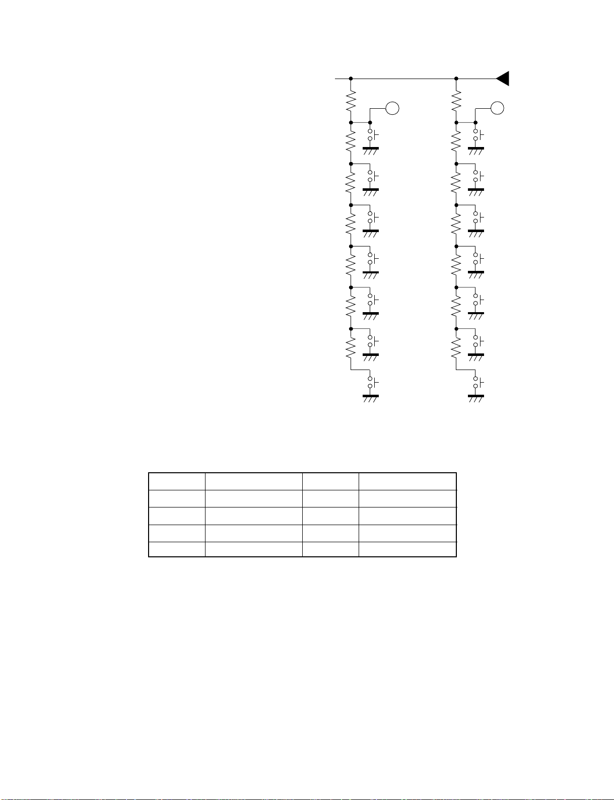
7. LOCAL KEY DETECTION METHOD
V
Local key detection in the N7SS chassis is carried out by
using analog like method which detects a voltage appears
at local key input terminals (pins 17, 18) of the microcomputer when a key is pushed. With this method using
two local key input terminals (pins 17, 18), key detection
up to maximum 14 keys will be carried out.
The circuit diagram shown left is the local key circuit. As
can be seen from the diagram, when one of key among
SA-01 to SA-08 is pressed, each of two input terminal
(pins 17, 18) developes a voltage VIN corresponding to the
key pressed. (The voltage measurement and key identification are carried out by an A/D converter inside the microcomputer and the software.
17
SA08
SA06
SA05
SA07
5
18
SA01
SA02
SA03
SA04
Key No.
SA01
SA-02
SA-03
SA-04
Table 4-2 Local key assignment
Function
DEMO START/STOP
POWER
CH UP
CH DN
Key No.
SA-05
SA-06
SA-07
SA-08
Fig. 4-6 Local key assignment
Function
VOL UP
VOL DN
ANT/VIDEO, ADV
MENU
4-8
Page 35

8. REMOTE CONTROL CODE ASSIGNMENT
Table 4-3
CUSTOM CODES ARE 40-BFH
Code
00H 0 Channel
01H 1 Channel
02H 2 Channel
03H 3 Channel
04H 4 Channel
05H 5 Channel
06H 6 Channel
07H 6 Channel
08H 8 Channel
09H 8 Channel
0AH 100 Channel
0BH ANT 1/2
0CH RESET
0DH AUDIO
0EH PICTURE/FUNC
0FH TV/VIDEO
10H MUTE
11H CHANNEL SEARCH
12H POWER
13H MT S
14H ADD/ERASE
15H TIMER/CLOCK
16H AUTO PROGRAM
17H CHANNEL RETURN
18H DSP/SUR (TV/CATV)
19H CONTROL UP
1AH VOLUME UP
1BH CHANNEL UP
1CH RECALL
1DH CONTROL DOWN
1EH VOLUME DOWN
1FH CHANNEL DOWN
40H PIP LOCATE
41H PIP LOCATE
42H PIP LOCATE
43H PIP LOCATE
44H CARVER
45H SURROUND UP
46H SURROUND DOWN
47H VOCAL ZOOM
48H CHANNEL LOCK
49H
4AH PIP CHANNEL UP
4BH
4CH
4DH
4EH PIP LOCATE (CH SEARCH)
4FH PIP SOURCE
Function to remote
PIP CHANNEL DOWN
PIP STILL/RELEASE
PIP ZOOM, ZOOM SIZE
Applicable
control
Applicable Conti-
to TV set nuty
Custom codes are 40-BFH
Code
50H PIP STILL
51H PIP ON/OFF
52H Do not use. Old type core power ON
53H PIP SWAP
54H PIC SIZE
55H DSP F/R
56H WIDE/SCROLL
57H CAPTION
58H EXIT
59H CYCLONE, SBS
5AH SET UP
5BH OPTION
5CH SUB WOOFER UP
5DH
5EH
5FH
80H MENU
81H EDS
82H ADV UP
83H ADV DWN
84H
85H GUIDE
86H THEME
87H LIST
88H PIP CONTROL
89H ENTER/TUNE
8AH PAGE UP
8BH DATA UP
8CH PAGE DN
8DH DATA DN
8EH CANCEL
8FH REC
90H
91H
92H Do not use. Old type core on.
93H
94H
95H
96H
97H NOISE CLEAN
98H
99H
9AH PIP VOLUME UP
9BH
9CH PIP CONTROL
9DH
9EH
9FH
Function to remote
SUB WOOFER DOWN
PIP VOLUME DOWN
Applicable
control
Applicable Conti-
to TV set nuty
4-9
Page 36

Custom codes are 40-BFH
Custom codes are 40-BFH
Code Applicable Conti-
A0H
A1H
A2H
Function
SUB-BRIGHT ADJUSTMENT
G. DRIVE ADJUSTMENT
B. DRIVE ADJUSTMENT
to TV set nuty
A3H
A4H
CUTOFF DRIVE 40H INITIALIZING, SCREEN, ADJ.
A5H R. CUTOFF ADJUSTMENT
A6H G. CUTOFF ADJUSTMENT
A7H B. CUTOFF ADJUSTMENT
A8H
MEMORY ALL AREA INITIALIZE
A9H PIP BRIGHT ADJUSTMENT
AAH
SUB CONTRAST ADJUSTMENT
ABH
HOR, VER PICTURE POSITON ADJUSTMENT
ACH SUB COLOR ADJUSTMENT
ADH SUB TINT ADJUSTMNET
AEH ADJUSTMENT-UP
AFH ADJUSTMENT-DOWN
B0H
SCREEN ADJ.: SERVICE
B1H DSP ON/OFF
B2H TEXT-1
B3H
TV/PIP VIDEO CHANGE-OVER
B4H CAPTION-1
B5H
B6H
B7H
TV/CABLE CHANGE-OVER IN SAME TIME ON MAN AND SUB
B8H HOTEL SETTING MENU
B9H DATA 4 TIMES SPEED UP
BAH DATA 4 TIMES SPEED DOWN
BBH
CHANGE-OVER OF HOTEL/NORMAL
BCH PIP CENTER
BDH M MODE
BEH CAPTON OFF
BFH ALL CHANNEL PRESET
C0H
C1H DIRECT WIDE 1
C2H DIRECT FULL
C3H
C4H
C5H
C6H
C7H
C8H
C9H
CAH
CBH
CCH
CDH
CEH
DFH
Code Applicable Conti-
Function
to TV set nuty
D0H
D1H
D2H Do not use. Old type core power ON
D3H
D4H
D5H
D6H
D7H PIP VIDEO ADJ.
D8H
STILL, FRAME ADVANCE
D9H
DAH SPEED
DBH
DCH ZOOM
DDH
DEH
DFH
E0H
PINCUTION/EW CORER (PARA/CNR)
E1H
VERTICAL S-CUVE CORRECTION/VERTICAL M-CURVE CORRECTION (VSC/FVC)
E2H
E3H
E4H
E5H
E6H
E7H
E8H
E9H
EAH
HORIZONTAL WIDTH (WID/PARA)
EBH
TRAPEZOIDE CORRECTION (TRAP)
ECH TEST TONE
EDH DOLBY
EEH
3 DIMENTIONAL Y/C SEPARATION
EFH DPC
E0H
STANDARD (HEIGHT LINEARITY) (VLIN/HIT)
E1H
WIDE (HEIGHT LINEARITY) (VLIN)
F2H SCROOL
F3H
WIDE 1, 2, 3
F4H
F5H
F6H
F7H
F8H
F9H
FAH
FBH
FCH
FDH
FEH
FFH
4-10
Page 37

9. ENTERING TO SERVICE MODE
11. SERVICE ADJUSTMENT
(1) Procedures
1) Press once MUTE key of remote hand unit to
indicate MUTE on screen.
2) Press again MUTE key of remote hand unit to
keep pressing until the next procedure.
3) In the status of above (2), wait for disappearing
of indication on screen.
4) In the status of above (3), press MENU (Channel
setting) key on TV set.
(2) Service mode is not memorized as the last-memory.
(3) During service mode, indication S is displayed at
upper right corner on screen.
10. TEST SIGNAL SELECTION
(1) In OFF state of test signal, SGA terminal (Pin 20)
and SGV terminal (Pin 21) are kept “L” condition.
(2) The function of VIDEO test signal selection is cy-
clically changed with VIDEO key (remote unit).
Table 4-4
Test signal
No.
0
1
2
3
4
5
6
7
8
9
10
11
Signal OFF
All black signal + R single color (OSD)
All black signal + G single color (OSD)
All black signal + B single color (OSD)
All black signal
All white signal
W/B
Black cross bar
White cross bar
Black cross hatch
White cross hatch
Black cross dot
Name of pattern
(1) ADJUSTMENT MENU INDICATION ON/OFF :
MENU key (on TV set)
(2) During display of adjustment menu, the followings
are effective.
1) Selection of adjustment item :
POS UP/DN key (on TV/Remote unit)
2) Adjustment of each item :
VOL UP/DN key (on TV/ Remote unit)
3) Direct selection of adjustment item
R CUTOFF: 1 POS (Remote unit)
G CUTOFF: 2 POS (Remote unit)
B CUTOFF: 3 POS (Remote unit)
4) Data setting for PC unit adjustment
SUB CONTRAST: 4 POS (Remote unit)
SUB COLOR: 5 POS (Remote unit)
SUB TINT: 6 POS (Remote unit)
5)
Screen adjustment mode ON/OFF: VIDEO
(TV)
6) Test signal selection: VIDEO (Remote unit)
* In service mode, serviceable items are limited.
(3) Test audio signal ON/OFF: 8 POS (Remote unit)
* Test audio signal: 1 kHz
(4) Self check display: 9 POS (Remote unit)
* Cyclic display (including ON/OFF)
(5) Initialization of memory :
CALL (Remote unit) + POS UP (TV)
(6) Initialization of self check data :
CALL (Remote unit) + POS DN (TV)
(7) BUS OFF :
CALL (Remote unit) + VOL UP (TV)
(8) Convergence adjustment pattern: 7 POS
Pushing once: Convergence adjustment mode
Pushing twice: Data memory
Pushing three times: Escaping from pattern.
12
White cross dot
(3) SGA (audio test signal) output should be square wave
of 1 kHz.
4-11
Page 38

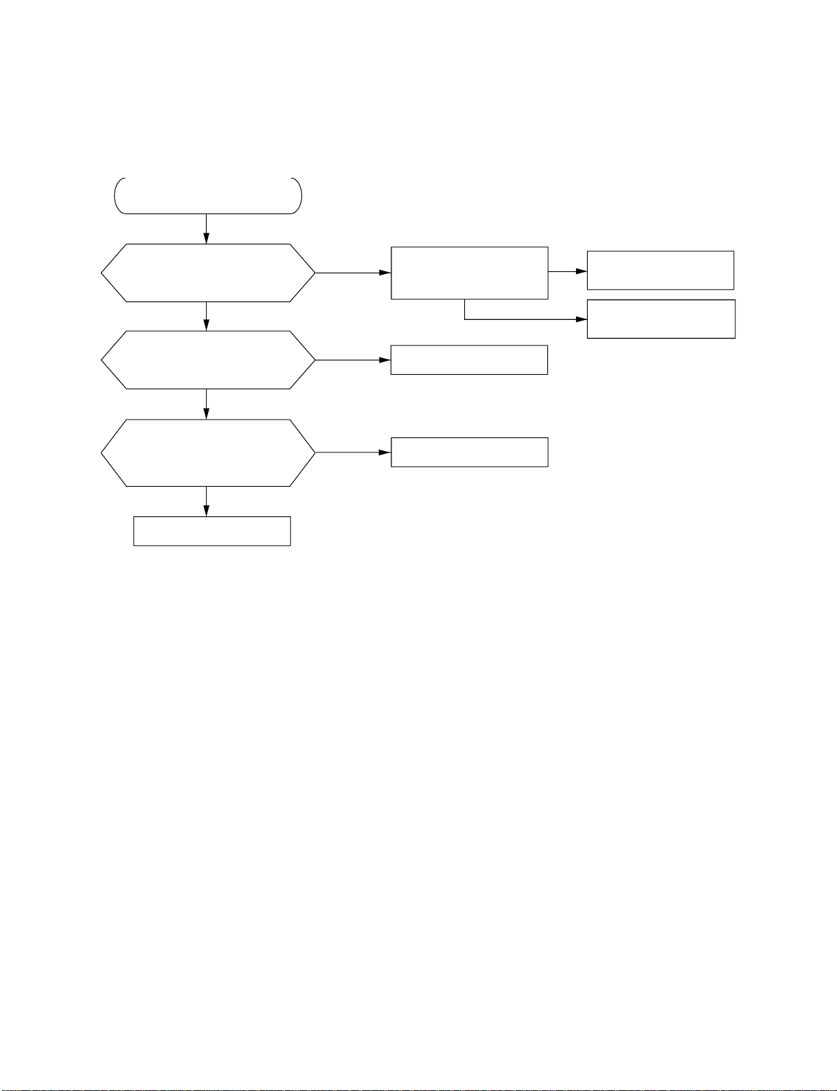
12. FAILURE DIAGNOSIS PROCEDURE
Model of N7SS chassis is equipped with self diagnosis function inside for trouble shooting.
12-1. Contens to be Confirmed by Customer
Table 4-5
Contents of self diagnosis
A. DISPLAY OF FAILURE INFORMATION
IN NO PICTURE (Condition of display)
1. When power protection circuit operates;
2
2. When I
C-BUS line is shorted;
Power indicator lamp blinks and picture does not come.
1. Power indicator red lamp blinks. (0.5 seconds interval)
2. Power indicator red lamp blinks. (1 seconds interval)
If these indications appear, repairing work is required.
Display items and actual operation
12-2. Contents to be Confirmed in Service Wo rk (Check in Self Diagnosis Mode)
Table 4-6
Contents of self diagnosis
Contents of self diagnosis
<Countermeasure in case that phenomenon always
arises.>
B. Detection of shortage in BUS line
C. Check of communication status in BUS line
D. Check of signal line by sync signal detection
E. Indication of part code of microcom. (QA01)
F. Number of operation of power protection circuit
Display items and actual operation
Display items and actual operation
(E xam ple of screen display)
SELF C HECK
N O . 239X XXX
PO W E R : 000000
BUS LINE: O K
BUS C ONT: O K
B L O C K : Q V 0 1 , Q V 0 1 S
Part coce of Q A01
N um ber of operation of
pow er protection circuit
Short check of bus line
C om m unication check of
busline
E
F
B
C
D
12-3. Executing Self Diagnosis Function
12-3-1. Procedures
(1) Set to service mode.
(2) Pressing “9” key on remote unit displays self diag-
nosis result on screen.
Every pressing changes mode as below.
SERVICE mode SELF DIAGNOSIS mode
(3) To exit from service mode, turn power off.
4-12
Page 39

12-4. Understanding Self Diagnosis Function Indication
In case that phenomenon always arises. See Fig. 4-7 .
(E xam ple of screen display)
SELF C HECK
N O . 239X XXX
PO W E R : 000000
BUS LINE: OK
BUS C ONT: OK
B L O C K : Q V 0 1 , Q V 0 1 S
Part coce of QA01
N um ber of operation of
pow er protection circuit
Short check of bus line
C om m unication check of
busline
Fig. 4-7
Table 4-5
E
F
B
C
D
Item
BUS LIME
BUS CONT
BLOCK: QV01
QV01S
Contents
Detection of bus line short
Communication state of bus line
The sync signal part in each video signal
supplied from each block is detected.
Then by checking the existence or non of
sync part, the result of self diagnosis is
displayed on screen. Besides, when "9"
key on remote unit is pressed, diagnosis
operation is first executed once.
Instruction os results
Indication of OK for normal result, NG for abnormal
Indication of OK for normal result
Indication of failure place in abnormality
(Failure place to be indicated)
QA02 NG, H001 NG, Q501 NG, H002 NG
QV01 NG, Q302 NG, QY02 NG, HY01 NG
QD04 NG, QM01 NG, Q701 NG
QA02 E2PROM, Q350 I/O EXP
H001 MTUN, QM30 C/C
Q501 VCD, QX40 JFORC
H002 MTS, Q701 DIG-CONV
QV01 AVSW, QZ01 YCS
Q302 E-WC, QX30 SLC
QY03 DUAL, QY01 PIP/VCD
HY01 PIP TUN, QK06 WAC
Note 1. The indication of failure place is only one place
though failure places are plural. When repair of a
failure place finishes, the next failure place is
inndicated. (The order of priority of indication is
left side.)
*Indication by color
• Normal block : Green
• Non diagnosis block : Cyan
4-13
Page 40

13-4-1. Clearing Method of Self diagnosis Result
In the error count state of screen, press “CHANNEL
DOWN” button on TV set pressing “Recall” button on
remote unit.
Caution:
Allways keep the following caution, in the state of service mode screen.
• Do not press “CHANNEL UP” button. This will cause
initialization of memory IC. (Replacement of memory
IC is required.
• Do not initialize self diagnosis result. This will change
user adjusting contents to factory setting value. (Adjustment is required.)
13-4-2. Method Utilizing Inner Signal
(VIDEO INPUT 1 terminal should be open.)
(1) With service mode screen, press VIDEO button on
remote unit. If inner video signal can be received,
QV01 and after are normal.
(2) With service mode screen, press “8” button on re-
mote unit. If sound of 1 kHz can be heard, QV01
and after are normal.
* By utilizing signal of VIDEO input terminal, each cir-
cuit can be checked. (Composite video signal, audio
signal)
White
Yellow
Cyan
Green
Magenta
Red
Blue
( COLOR BAR SIGNAL)
Color elements are positioned in sequence of high brightness.
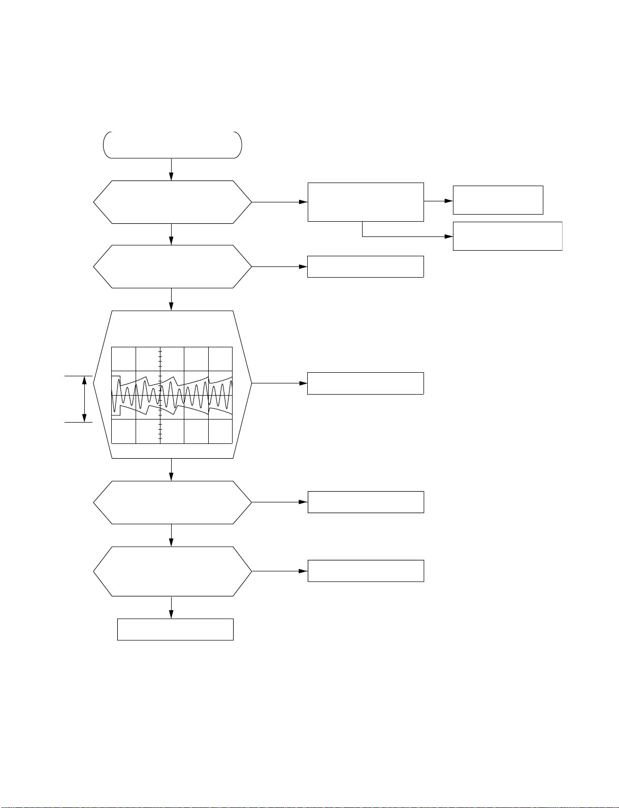
13. TROUBLE SHOOTING CHART
13-1. TV does not turn ON.
Key on TV
Voltage change at pins 17, 18 of
QA01 (5V to 0V).
OK
Replace QA01.
Remote unit key
Pulse input at pin 35 of QA01,
When remote unit key is pressed.
OK
Fig. 4-8
NG
Check key-in circuit.
NG
Replace QA01
Check tuner power circuit.
Fig. 4-9
4-14
Page 41

13-2. No Acception of Ke y-IN
Key on TV
Voltage change at pins 17, 18 of
QA01 (5V to 0V).
OK
Replace QA01.
Remote unit key
Pulse input at pin 35 of QA01,
When remote unit key is pressed.
OK
Replace QA01
NG
Check key-in circuit.
NG
Check tuner power circuit.
Fig. 4-10
13-3. No Picture (Snow Noise)
No picture
Voltage at pins of +5V and 32V.
OK
Check H001. Check tuner power circuit.
NG
Fig. 4-11
4-15
Page 42

13-4. Memory Circuit Check
Memory circuit check
Voltage check at pin 8 of QA02 (5V).
NG
Pulse input at pins 5 and 6 of QA02
in memorizing operation.
Replace QA02.
Adjust items of TV set adjustment.
13-5. No Indication on Screen
No indication on screen.
OK
NG
OK
Note: Use replacement parts for QA02.
Fig. 4-12
Check power circuit.
Check QA01.
Check of character signal at pin 23
of QA01. (5V(p-p))
OK
Input of OSC waveform at pin 29 of QA01
with indication key pressed.
OK
Check of sync signal at pins 26, 27 of QA01.
OK
Replace QA01.
Fig. 4-13
NG
Check V/C/D circuit.
NG
Check OSC circuit.
Check sync circuit.
4-16
Page 43

SECTION V
VIDEO CIRCUIT
5-1
Page 44

1. A/V SELECTOR CIRCUIT
1-2. Speifications
1-1. General
The A/V selector circuit selects the video and audio signals from the tuner and external device. Selection of signals is controlled by the microcomputer through the I2C
bus.
U/V tuner (main)
IMA
H001, H002
Equalizer
~QV43
QV40
4
5 6
TIF
HY01
2
V L V R
TV2 TV1
Internal input
External input
Output
Table 5-1
U/V tuner (Main)
U/V tuner (Sub)
Video 1 (with S terminal)
Video 2
Video 3 (Front) (with S terminal)
Video output (V, L, R)
R
43
(Main)
L
To audio SW
45
To monitor output
Video 1
Video 2
Video 3
Y
C
V
L
R
V
L
R
Y
C
V
L
R
9
11
7
10
50
51
49
21
23
19
20
22
8
Y
C
V
L
R
V
L
R
Y
C
V
L
R
E1
QV01
TA8851CN
E2
E3
Fig. 5-1 Block diagram of the A/V selector circuit
(Main)
(Main)
Input
(Main)
Output
(Sub)
Output
Y or V
V
46
3D
Y
48
C
40
C
42
Y
44
C
32
34
comb filter
To Q501
To DUAL unit
5-2
Page 45

1-3. Operation of the Circuit
1-3-1. Composite Video Signal
The selected video signal is sent to pin 46 of QV01, YCseparated through the comb filter, applied to pins 40 & 48
and output to pins 42 & 46 of QV01, then supplied to
Q501 (V/C/D).
The video signal for the subscreen is sent to pins 32 and
34, then supplied to the dual unit.
VT1
5
VB1/Y121
VT2
VB2/Y122
VE1
VE2
VE3
YE1
YE2
YE3
CE1
CE2
CE3
TV1R
MAIN R
SUB R
E1R
M/N (E4) R
E3 R
TV1L
MAIN L
SUB L
E1L
M/N (E4) L
E3L
50
2
53
7
DAC
13
DAC
19
DAC
9
15
21
11
17
23
6
49
3
I
2
52
DAC
10
16
22
4
51
1
I
4
54
DAC
8
14
20
ST1
ST2
SE1
SE2
SY1
SY2
SC1
SC2
SR1
SR2
SL1
SL2
6dB
AMP
6dB
AMP
6dB
AMP
6dB
AMP
1-3-2. S-video Signal
When the cable is connected to the S-terminal, the internal switch of the S-terminal is shorted with GND, each Vterminal (composite video terminal) of QV01 drops in bias
level through the resistor, and QV01 sends the Y/C signal
of the selected channel directly to pins 42 and 44.
SV1
SV2
Speaker audio SW
PIP output SW
SRT
PIP output SW
SLT
RB2, LB2,
VE1, VE2, VE3
18 12 24
Vcc GND1 GND2
6dB
AMP
6dB
AMP
Clamp(1)
SOY1
SOC1
Clamp(2)
SOY2
SOC2
I/O
2
C
I
DAC
Mute
VO1
46
fcl1
47
YI11
48
YO1
49
CO1
42
CI1
40
VO2
36
fcl2
37
YI12
38
YO2
34
CO2
32
CI2
30
SPK-OUT R
39
SPK-OUT L
41
MAIN-OUT R
43
MAIN-OUT L
45
PIP-OUT R
33
PIP-OUT L
35
O3
31
I/O1
28
I/O2
29
SDA
26
SCL
27
Mute
25
Fig. 5-2 Block diagram of QV01 (TA8851CN)
5-3
Page 46

2. VIDEO PROCESSING CIRCUIT
R
2-1. General
Fig. 5-1 shows the video signal block diagram. The flow
of signal is explained in this section. The video signal
which is selected with the A/V selector circuit is applied
to pins 15 and 13 of Q501 as Y/C signals. The Y-signal is
unchanged, the C-signal is color demodulated with Q501,
then the signals are sent to pins 4, 5 and 6 as a YIQ signal.
The YIQ signal is horizontally compressed in WAC, superimposed on the subscreen in DW, and applied to the
UP CON, where it is double-speed converted and the horizontal frequency is converted to 31.5 kHz. The converted
YIQ signal is sent to pins 53, 52 and 51 of Q501.
Q501 controls brightness, unicolor, color density and tone,
corrects picture quality, and switches OSD and C/C, then
the signal is developed from pins 43, 42 and 41 and applied to the CRT drive circuit.
A/V SW
QV01
Sub Y/C
2-2. V/C/D IC (Q501)
2-2-1. TA1259N
The video signal processing is carried out by Q501. The
IC is improved to be a wide bandwidth mainly in the signal processing circuit so that the past IC (T A1222AN) may
perform the video process for the up-conv erted NTSC signal. The following describes the main terminal information of Q501.
UV TUNER
(MAIN)
UV TUNER
(SUB)
EXT VIDEO
Pin 1~3
Main Y/C
Main Y/C
3-D Comb
Filter
(Y)
15
(C)
13
DW
WAC
4
5
Color
Decode
Y,I,Q
6
I,Q
Fig. 5-3
Y, I, Q
Q501
V/C
YIQ
proc.
RGB
MATRIX
UP CON
Y. I. Q
51
52 53
RGB
SW
43
42
41
R.G.B
To
CRT-D
5-4
Page 47

Table 5-2
Pin No.
1
2
10
11
17
18
23
24
25
30
31
32
36
45
Pin Name
CW output
SCP output
X'tal
APC filter
Sync input
Sync output
Clamp input
Mask pulse input
Blanking input
HD output
VD output
YS input
OSD-YS input
ABL input
Descriptions
3.58 MHz signal synchronized with burst signal is output.
The signal is superimposed by the burst gate pulse and the blanking pulse. The signal
is used for the video signal clamping.
3.58 MHz oscillation crystal terminal.
Phase detection terminal for color synchronization (also used for oscillation frequency
control)
Sync signal input terminal. Y signal is input.
The sync signal sync-separated is output. Used for no signal detection in microcom-
puter.
Clamp pulse input terminal synchronized with Y signal input to pin 53.
Masking pulse input terminal for black extension prevention synchronized with Y signal
input to pin 53.
Blanking pulse input terminal synchronised with Y signal input to pin 53.
Horizontal pulse synchronized with Y signal input to pin 15.
Vertical pulse synchronised with Y signal input to pin 15.
Switching pulse for multi-language broadcast display.
Switching pulse for OSD display.
ABL control input terminal.
47
49
50
54
55
YM input
APL detection
Black detection
COL
DAC 1
Half tone switching pulse at OSD display.
Detects an average level of the video signal for direct current transmission correction.
Black area of the video signal for black extension circuit is detected.
Used for color limiter peak hold.
Test point (TP501). In service mode, adjustment waveform is observed.
5-5
Page 48

GND (DEF) Vcc (DEF)
17
20
21
25
24
19
22 23
GND
Vcc (5V)
16
15
13
14
12
11
10
9
8
H. V.
SYNC SEP
V. SEP
V.
SYNC SEP
SYNC CHIP
CLAMP
SW
ACC AMP
ACC DET
APC DET
CHROMA
VCO
PHASE DET
<APC-1>
DELAY
LINE
TOF
SUB
COLOR
P/N IDENT
DET
C W
MATRIX
FILTER
AUTO ADJ
32 FH VCO
H.
COUNT DOWN
Fsc TRAP
BPF
SW
CHROMA
BLK
CHROMA
DEMOD.
L.P.F.
FSC TRAP
H. BLK
SW
S
R
T
GAMMA
CORRECTION
D.C.
RESTORE
SHARPNESS
DELAY LINE
SHARPNESS
CONTROL
WPS
V.
COUNT DOWN
D/A
CONVERTER
DELAY LINE
BLACK
LEVEL COR.
A.P.L. DET
HPF
T. NR AMP SUB CONT
HALF TONE
REGISTER
DELAY LINE
BLACK
STRETCH
BLACK
PEAK DET
VM AMP VM MUTE
CLAMP
V.P. OUT
SYNC
I2C BUS
DECODER
Y. CLAMP
Y
WHITE
PEAK DET
UNI COLOR
OUT
S W
TOR
31
18
27
26
28
4
GND
29
53
50
49
48
Vcc
40
(9V)
5
6
51
52
54
55
56
3
IQ/UV
CLAMP
UNI COLOR
SECAM
CONTROL
CW OUT
1
FRESH
COLOR
COLOR
AXIS
G-Y MATRIX
COLOR
PEAK DET
HI BRIGHT
COLOR
COLOR
SYS IDENT
1H DL
CONTROL
7
IQ UV
CONVERT
TINF
CLAMP
CDE
DEC 1/2
S.C.P.
OUT
2
S W
DELAY
LINE
HALF
TONE
COLOR
GAMMA
HD OUT
EXT BPP IN
30
Fig. 5-4
RGB
MATRIX
POWER OFF IN
YM SW
47
RGB
BRIGHT
S W
DRIVE CLAMP
Vcc (9V) GND
40 44
CLAMP
CLAMP OSD AMP
PEAK
ACL DET
CONTRAST
YS SW
YS SW
ABCL AMP
BLK
RGB OUTCUT OFF
41 42 43
33
34
35
36
37
38
39
32
45
5-6
Page 49

3. CRT OUTPUT CIRCUIT
3-1. General
The CRT output circuit is composed of a cascade connection, RGB output circuit using DC bias circuit, white width
improvement circuit and a blue extension circuit. As shown
in Fig. 5-5, the white width improvement circuit and DC
bias circuit are included in the R drive unit and the blue
extension circuit in the B drive unit.
R-DR IVE
+220V
9V
R-out
R 932/R 931/R 936
KR
Q901
FIN E W HITE
CIRCUIT
Q962
DC Bias
9V
G -out
3-2. Output Circuit
Among the output circuits, R- out circuit is shown in Fig.
5-6. The output transistor Q901 is connected to Q913 in
the output is developed at the collector. The DC bias voltage is set to the same voltage level as the emitter voltage
of Q913 in the cut off and determines the AC gain. T he
cutoff voltage is determined by R916, R914 & R931//
R932//R936 and the cutoff voltage (R CUTOFF) of R out
signal. This is shown by the following equation.
V
CUTOFF
(220 - R931//R932//R936) (
C914, L912 and L913 are used for correcting the frequency
response and each operates as a high frequency peaking
filter.
=
R
CUTOFF
-
0.7 - 0.7
R916 R914
+220V
R 941/R 942/R 943
Q911
Fig. 5-5
)
Q 9501
G -DR IVE B-D RIVE
KG
+220V
R932
R931
9V
Q901
R914
R917
R-out
Q913
R916
+220V
+9V
B-out
R-DRIVE
R936
R948L912
R949 R913
L913
R915+R919
C914
R918
R 951/R 952/R 953
KB
Q921
BLUE
EXTENSIO N
Q 9603
KR
DC Bias
Fig. 5-6
5-7
Page 50
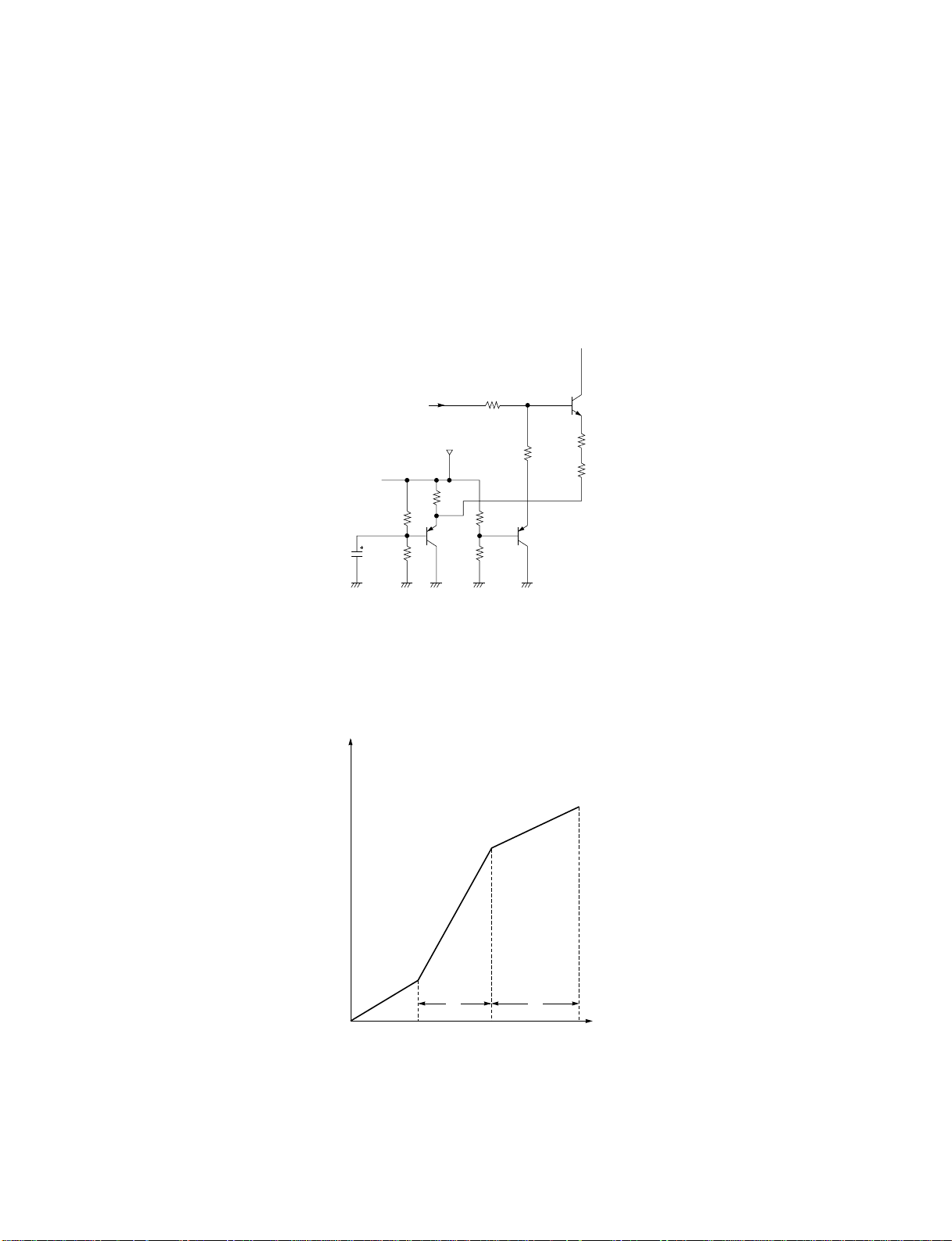
3-3. Blue Extension Circuit
R
The blue extension circuit controls Q921 emitter current
depending on the B-out level and corrects the B-CRT luminance characteristic, thereby obtaining even white le vel.
When B-out level rises and the base voltage le vel of Q9605
exceeds the cut off lev el specified by the emitter of Q9601,
Q9605 turns ON and the gain of Q921 rises. ("B" area in
Fig. 5-8)
B-Y
9V
R9604
R9605
Q9601
C9602
R9606
After that, if the level rises furthermore, Q9602 turns ON
and mutes Q9605. ("C" area in Fig. 5-8)
Due to above operations, B-drive input/output characteristics as shown in Fig. 5-8 is obtained.
Q921
To EMITTE
R956
Q9605
R9613
R9601
R9614
R9602
Q9602
R9603
KB
Fig. 5-7
C B
B-out
Fig. 5-8
5-8
Page 51

SECTION VI
YCS/DUAL CIRCUIT
6-1
Page 52

1. GENERAL
3. CIRCUIT OPERATION
The YCS/DUAL circuit puts YCS and DUAL on the same
PCB to share the memory IC. This circuit comprises the
following 3 blocks.
• DUAL block
• YCS block
2. OPERATION PRINCIPLE
2-1. DU AL Block
This is the circuit to process signals of the subscreen, and
has the following functions.
• Compressing the subscreen of the double window to 1/
2
• Still picture of subscreen
• 9-screen multi-search
• OSD superimpose (only at 9-screen multi-search)
• Main/sub screen images superimpose with YIQ signal.
2-2. YCS (3-dimension YCS Separator)
Block
The 3-dimension YCS separator is the comb filter using
the frame memory, and separates ideally the bright signal
and color signal with respect to a still picture, providing a
clean image without:
• Dot disturbance generated a t the color BOUNDARY
• Exudation of color in the vertical direction (cross-color)
However, separation fails in the moving picture because
the picture moves in the front/rear frames.
The YCS block detects motion, and s witches the separation mode: the 2-dimension YC se paration using a line
memory for a moving picture, and the 3-dimension YC
separation for a still picture. These two separation modes
compensate each other and result in ideal YC separ ation.
2-3. Memory Selector Block
This selects the memory use state in:
• 2-screen (9-screen): DUAL
• 1-screen: YCS
The switching is controlled with pin 20 of QY03 (MOH)
in the DUAL block.
Fig. 6-1 shows the block diagram of YCS/DUAL.
3-1. DUAL Section
The POP video signal is supplied from pin 8 of PY01, and
is applied to pin 4 of QZ100 (DIGITAL COMB). The Y
and C signals from pin 15 and 13 are applied to pin 40 (Y
IN) and pin 6 (CHROMA IN) of QY01(V/C/D IC) respectively.
The Y, I, Q signals from pin 37, pins 48 and 47 of QY01
are limited in their bands in the LPF which eliminates a
folded distortion, and then applied to pin 8 (YIN), pin 14
(IIN), and pin 16 (PIN) of QY03 (TC90A17F) respectively .
The synchronizing signal in the write channel is generated from the VD signal at pin 13 of QY01 and the HD
signal at pin 14, and is applied to pins 21 (WVD) and 22
(WHD) of QY03 respectively.
The synchronizing signal in the read channel is supplied
from pins Y11 and Y12 of PY01, and is applied to pins 79
(RVD) and 78 (RHD) of QY03 r espectively.
The video signal which was converted to digital data is
supplied from pins 33 to 40 and pins 42 to 49 of QY03.
The RMCK, WMCK, RRST and WRST signals in the clock
channel are supplied from pins 69, 27, 68 and 32 respectively. These signals are supplied to the memory of QY06
and QY07.
The digital data from QY06 and QY07 is applied to pins
51 to 58 and pins 59 to 66 of QY03. This signal is also
supplied to QZ01. But, the input data is ignored, because
the I2C BUS is set to make the input/output pin of QZ01
high/high impedance and turns off in the three-dimension.
The Y, I and Q signals, the video signal of the subscreen,
from pins 96, 98 and 100 of QY03 pass through the LPF
which eliminates a clock component, and are applied to
pins 29, 30 and 31 of QY01, the main/sub video signal
superimposing circuit. The video signal of the main screen
is supplied from pins 1, 2 and 3 of PZ01, and is applied to
pins 25, 26 and 27 of QY01. The Ys signal, which is the
main/sub video signals selector signal, is led from pin 71
of QY03.
The video signal superimposed with the main/sub video
signals is generated from pins Y04, Y05 and Y06 of PY01.
The I2C BUS data from the main microcomputer is supplied from pins DI and DJ of PZ01, and is applied to pins
82 and 83 of QY03.
6-2
Page 53

3-2. YCS Section
4. TERMINAL DESCRIPTION
The video signal from the AV selector is applied to the
input terminal (DG). The input video signal is limited in
their bands in the LPF which eliminates a folded distortion, and is applied to pin 70 of QZ01.
The video signal, that was converted to digital data, is
applied to pins 32 to 39, 47 to 54 of QZ01. The MEMCK,
RRST, WEN1, WEN0, REN1 and REN0 signals of the
clock channel are applied to pins 30, 41, 42, 43, 44 and 45
respectively. These signals are input to QY06 and QY07
memory via QZ26 (TC74LVX244).
The digital data from QY06 and QY07 is applied to pins
13 to 28 of QZ01. This signal is also supplied to QY03.
But, the input data is ignored, because the analog signals
(Y, I, Q) of QY03 are muted.
The luminance signal generated at pin 83 of QZ01 is amplified in the LPF which eliminates the clock component,
and the gain amplifier, and then it is outputted from the
(DC) terminal as a luminance signal.
The color signal generated at pin 71 of QZ01 is eliminated its clock component in the LPF, amplified in the
gain amplifier, and outputted from the (DD) terminal as a
color signal.
The system clock to perform Y/C separation operation is
a signal of 28.6 MHz components (entered pin 98) abstracted from the waveform, which are generated at pin
90 on the crystal oscillation basis connected to pins 5 and
6 of QZ01, through BPF (band pass filter).
The PLL (phase locked loop) control is carried out so that
the clock signal is locked to the input video signal.
4-1. PY01
No.
Y01
Y02
Y03
Y04
Y05
Y06
Y07
Y08
Y09
Y10
Y11
Y12
Y13
Y14
Y15
4-2. PZ01
No.
Table 6-1
Signal name, Voltage, etc.
Main screen period: 0V,
Subscreen period: 5V
5V at operating
GND
Q-signal output
Y-signal output
I-signal output
GND
POP video input
POP Y OUT
GND
Vertical synchronizing signal, negative
polarity, 5V
Horizontal synchronizing signal, negative
polarity, 5V
POP VD OUT
PMK (5V ± 0.5V)
POP C INPUT (0.6V (p-p) at burst)
Table 6-2
Signal name, Voltage, etc.
6-3
1
2
3
4
5
DH
DC
DE
DD
DB
DG
DA
DF
DI
DJ
Main screen Q-signal input
Main screen I-signal input
Main screen Y-signal input
Sandcastle pulse, positive polarity
GND
Comb-through, 3.3V
Y comb 2V (p-p)
+9V±0.5V
C comb 0.6V (p-p) at burst
GND
V-AV 2V (p-p)
+5V±0.5V
¾¾
I2C BUS data, 5V
I2C BUS clock, 5V
Page 54

4-3. QZ01 (TC90A28F)
Table 6-3
Pin
No.
1
2
3
4
5
6
7
8
9
10
11
12
13
14
15
16
Name
CK8
MEMHZ
MUSEMD
VDD
XI
XO
VSS
KILIN
ACNOUT
SCL
SDA
VDD
FMI0
FMI1
FMI2
FMI3
I/O
I
System clock input
I
Memory Hi-Z control
I
MUSE control input
—
3.3V
I
X'tal IN
O
X'tal OUT
—
GND
I
Color killer input
O
I2C bus I/O control
I
I2C bus clock
I/O
I2C bus data
—
3.3V
I
Memory data input (LSB)
I
Memory data input
I
Memory data input
I
Memory data input
Function
Pin
No.
37
38
39
40
41
42
43
44
45
46
47
48
49
50
51
52
Name
FMO10
FMO9
FMO8
VSS
RRST
WEN1
WEN0
REN1
REN0
VDD
FMO7
FMO6
FMO5
FMO4
FMO3
FMO2
I/O
O
Memory data output
O
Memory data output
O
Memory data output
—
GND
O
Memory R/W reset
O
Memory write enable 1
O
Memory write enable 0
O
Memory read enable 1
O
Memory read enable 0
—
3.3V
O
Memory data output
O
Memory data output
O
Memory data output
O
Memory data output
O
Memory data output
O
Memory data output
Function
17
18
19
20
21
22
23
24
25
26
27
28
29
30
31
32
33
FMI4
FMI5
FMI6
FMI7
FMI8
FMI9
FMI10
FMI11
FMI12
FMI13
FMI14
FMI15
VSS
MEMCK
VDD
FMO15
FMO14
I
Memory data input
I
Memory data input
I
Memory data input
I
Memory data input
I
Memory data input
I
Memory data input
I
Memory data input
I
Memory data input
I
Memory data input
I
Memory data input
I
Memory data input
I
Memory data input (MSB)
—
GND
O
Clock for memory
—
3.3V
O
Memory data output (MSB)
O
Memory data output
53
54
55
56
57
58
59
60
61
62
63
64
65
66
67
68
69
FMO1
FMO0
VSS
VDD
HREF
VIN
VCDBUS
BLK
DCCLMP
TEST2
TEST1
RESET
VSS
VDD
VSS
YVR2
AVDD
O
Memory data output
O
Memory data output (LSB)
—
GND
—
3.3V
O
H reference timing output
I
Vertical timing input
O
Serial bus
O
Blanking timing output
O
Clamp pulse output
I
Test terminal
I
Test terminal
I
Reset
—
GND
—
3.3V
—
GND
—
A/D reference (for Y)
—
3.3V (analog)
34
35
36
FMO13
FMO12
FMO11
O
Memory data output
O
Memory data output
O
Memory data output
6-4
70
71
72
VIDEO IN
AVSS
YVR1
I
Composite /Y video input
—
GND (analog)
—
A/D reference (for Y)
Page 55

Pin
No.
Name
I/O
Function
73
74
75
76
77
78
79
80
81
82
83
84
85
86
87
88
89
BIAS
YVR2
AVDD
CIN
AVSS
CVR1
BIAS1C
AVDD
COUT
AVSS
YOUT
AVDD
BIAS1Y
VREFYC
BIAS2YC
BIAS1CK
AVSS
A/D bias (for Y/C)
—
A/D reference (for C)
—
3.3V (analog)
—
C video input
I
GND (analog)
—
A/D reference (for C)
—
D/A bias 1 (for C)
—
3.3V (analog)
—
C video output
O
GND (analog)
—
Y video output
O
3.3V (analog)
—
D/A bias 1 (for Y)
—
D/A reference voltage (for Y/C)
I
D/A bias 2 (for Y/C)
—
D/A bias 1 (for C)
—
GND (analog)
—
90
91
92
93
94
95
96
97
98
99
100
CK1
AVDD
VREFCK
BIAS2CK
VDD
VSS
VDD
VSS
BPF421
VDD
CKOUT
Clock output
O
3.3V (analog)
—
D/A reference (for clock play-
I
back)
—
D/A bias 2 (for clock playback)
—
3.3V
—
GND
—
3.3V
—
GND (for self bias)
O
1820 fH abstraction
—
3.3V (for self bias)
O
1820 fH clock output
6-5
Page 56

5. YCS TROUBLESHOOTING
YCS FAILURE DIAGNOSIS
No main screen picture
Does picture appear at S-input?
Y
PZ01 :
Are there following signals?
(DA) 5V, (DE) 9V, (DG) Video
Y
Is video signal obtained
at (70)pin of QZ01?
Y
Is signal level of 1~2V obtained
at (70)pin of QZ01?
Y
N
N
N
N
Check circuits except YCS.
Check QZ06, QZ07.
2
Check I C bus;
(10)pin and (11)pin of QZ10.
Are C and Y signals obtained
at (81)pin and (83)pin of QZ01?
Y
Is C-output obtained at PZ01 (DD)?
Y
Is Y-output obtained at PZ01 (DC)?
Y
Check circuits except YCS.
N
N
N
Fig. 6-1
QZ01 (6)pin, (98)pin clock check.
Check QZ02, QZ23, QZ24.
Check QZ03, QZ20, QZ21, QZ22.
6-6
Page 57
6. BLOCK DIAGRAM
PY01
Y01
Y02
Y03
Y04
Y05
Y06
Y07
Y08
Y09
Y10
Y11
Y12
Y13
Y14
Y15
Q Z100
TC 9C A 15P
Q Y01 TA1270F
R(I)
40
Y IN
B (Q)
C IN
VD
HD
6
Q Y 03 TC 9C A17F
71
Ys O UT
PW R ST
92
Y
37
LPF
48
LPF
LPF
47
13
14
QY42
1
13
LP F
LP F
LP F
14
16
21
22
79
78
82
83
20
96
98
100
8
YIN
I IN
Q IN
WVD
WED
RVD
RED
SCL
SDA
MOH
YO UT
(I) O U T
(Q ) O U T
RHREF
WCK
W HREF
DATA IN
DATA OUT
WMCK
RMCK
RRST
WRST
RCK
REN
76
75
24
25
57~58
57~58
42~47
33~40
67
27
69
68
32
PLL
PLL
PZ01
(1 )
(2 )
(3 )
(4 )
(5 )
(DH)
(DC)
(D E )
(DD)
(D B )
(D G )
(D A )
(D F )
(D I)
(D J )
AM P.
AM P.
QY01
TA 1270F
Ys
SUB-Display
S uperim posing
output
Main-Display
LPF
LP F
LP F
QY66
QZ01
TC 90A 28F
KILL
8
YOUT
83
81
COUT
VIDEO IN
70
MEMHZ
2
11
SDA
SCL
10
EN (D )
IN
IN
EN (Y)
MEMCK
WEN
REN
DATA OUT
DATA IN
QY63
74LV X 244
RRST
42 43
44 45
32~39
47~54
13~28
OUT
OUT
30
41
Q Y 06,Q Y 07
DATA
IN
CK,RST
IN
IE , R E
EN
IN O U T
QZ26
74LV X244
DATA
OUT
Fig. 6-2 Block diagram of YCS/DUAL circuit
6-7
Page 58

This page is not printed.
6-8
Page 59

SECTION VII
DOUBLE-SPEED CIRCUIT (UPCON)
7-1
Page 60

1. GENERAL
2. CIRCUIT OPERATION
The double-speed circuit converts an interlaced scanning
frequency signal of approx. 15.75 kHz horizontal frequency
in the NTSC system to the progressive scanning signal of
motion adaptive type and approx. 31.5 kHz horizontal frequency.
2-1. Signal Flow
Fig. 7-1 shows the block diagram of this circuit.
2-1-1. Input Section
The Y-signal (luminance signal) applied to pin 214 of PX01
is applied to the pin 63 of QX100, A/D converter, through
the 6dB amplifier and the low-pass filter. The I and Q signals (color signals) are applied to pins 50 and 31 of QX100
through the amplifier and the low-pass filter, like the Ysignal which is applied to pins 216 and 218 of PX01.
The Y/I/Q signals are clamped in the internal clamp circuit, and are converted to digital signals. The Y-signal is
developed from pins 6 to 13 as an 8-bit data, and is applied to QX300. The I/Q signals are 8-bit data that are IQ
multiplexed and developed from pins 17 to 24 as a C-signal, and is applied directly to QX400 without passing
through QX300.
2-1-2. Motion Adaptive Type Progressive Scanning
Line Number Conversion Section
The scanning line number changing IC QX300 (SLC)
changes the number of scanning lines by applying the Ysignal input at pins 136 to 129 to the built-in line memory
and the external field memory of QX310 and QX320.
Detecting the video signal movement, make the still portion fine flicker-free image with vertical resolution by developing the previous field signal, and develops the signal
generated from the current filed for the moving portion.
For the Y-signal processed as above, output the interpolation signal processed matching the moving portion and
still portion from pins 39 to 42, and output the direct signal which is the input signal to be developed directly as an
output from pins 43 to 47. The interpolation and direct
output signal are 8-bit 14.3 MHz in the IC, but multiplexed
to 4-bit 28.6 MHz in MSB and LSB sides when it is developed.
7-2
Page 61

2-1-3. Double-speed Converter Section
The Y/I/Q signals are processed with the double-speed
converter/vertical expansion-compression IC QX400
(JFORC), external field memory QX440 and QX450 and
the line memory QX460, QX465, QX470 and QX480.
The interpolation and direct Y-signals which were changed
in the number of scanning lines are applied to pins 198 to
195 and 192 to 189. The I/Q signals are multiplexed as
described above and are applied to pins 209 to 202.
The rate of Y signal is impr oved from approx. 15.75 kHz
horizontal frequency to 31.5 kHz using line memories of
QX470 and QX480. Then the switch built-in inside QX400
switches the signal for an interpolation signal and a direct
signal and develops on y signal (motion adapti v e type progressive scanning signal).
On the other hand, the rate of I and Q signals is improved
from approx. 15.75 kHz horizontal frequency to 31.5 kHz
using line memories of QX460 and QX465 in the same
way as Y signal. Then the same signal is converted into
two line signals.
Thus processed Y/I/Q signals are developed as 8-bit data
from pins 18 to 11, 42 to 35 and 28 to 21 pins, respectively.
The field memory of QX440 and QX450 is used to match
the phase between the developed Y/I/Q signals and output
sync system signal.
2-2. Clock/Sync Signal
All the clock signals used in the (a) input section, (b) motion adaptive type progressive scanning line number conversion section, (c) double converter section and (d) output section are generated from HD synchronized with the
input video signal. The signals are generated at PLL IC
QX210 and its clock frequency is approx. 28.6 MHz.
HD/VD out signals are developed from pins 235 and 234
of QX400 to pins 210 and 212 of PX06 directly. SCP out
signal adds a horizontal mask signal at pin 7 of QX400
and a clamp signal which changes the signal width by a
mono-stable multi-vibrator QX456. Then the signals are
developed from pin 202 of PX01.
VMSK out signal develops from pin 6 of X400 to pin 201
of PX01 directly.
2-3. I2C BUS
Setting of the processing conditions of QX300 and QX400
are controlled by the I2C BUS clock and data applied to
pins 51 and 53 of PX04.
2-1-4. Output Section
The Y/I/Q signals from QX400 are applied to pins 1 to 8,
9 to 16 and 18 to 25 of QX500, the D/A converter, respectively. The Y/I/Q signals which are converted to analog
signals in QX500 are developed from pins 40, 38 and 36,
respectively, and then they are developed from pin 204,
206 and 208 of PX01, respectively, through the low-pass
filter.
7-3
Page 62

3. BLOCK DIAGRAM
K
3
J-RST
SDA
2
3
4
J-RST
SDA
SCL
80
OUT
93
IN
128
OUT
IN
139
QX440
UPD42280GU
UPD485505G
QX460,QX465
PX05
CM
CI
3
GND
SCL
1
34
TST1,2
33
SDA
223
SCL
224
71
~
82
~
~
118
130
~
GND
HD out
GND
VD out
N.C.
PX06
209
1
21
210
212
CLP
5
QX456
TC74HC123
2
94
OUT
QX450
42280GU
UPD
IN
OUT
IN
485505G
UPD
QX470
OUT
QX480
UPD
485505G
IN
~
106
~
141
~
149
~
160
~
170
~
.MAS
V
PX01
201
HMSK
QX500
6
7
234
VDout
VBLK
HBLK
235
HDout
104
YM
116
148
YP
158
168
YD
179
YD in
~~ ~
195
out
SCP
GND
2Y
GND
2I out
202
203
204
205
206
LPF
Y out
Y in
MB40978PFQ
1
~~~
11
~~~
Y out
198
189
LPF
40
38
I out
I in
8
9
18
35
I out
QX400
YI in
192
GND
2Q out
207
208
LPF
36
Qout
Q in
18
16
42
TC183E2550F02
25
VD in
238
45
CLKB in
HREF out
5
21
28
Q out
C(I) in
202
HD in
CKA in
2
239
209
39
42
43
25
~~
28
OUT
QX320
QX310
2
1
PX03
GND
+5V-D
UPD
UPD
3
GND
42280GU
42280GU
IN
OUT
IN
4
+5V-D
~
21
24
~
3
6
~
MDL
7
10
~
QX300
TC90A04F
6
7
5
GND
GND
+5V-A
YFD
8
+9V-1
YMV
QX100
TLC5733AIPM
213
PX02
GND
47
SDA
I in
50
LPF
AMP.
216
I in
SCL
CK8in
Href
Vref
VD in
217
GND
15
14
12
127
128
16
17
24
C out
Q in
31
LPF
QX801
AMP.
218
Q in
219
GND
220
HD in
221
GND
222
VD in
YIV
V in
129
136
~
6
13
~~
Y out
Y in
63
LPF
AMP.
215
214
Y in
GND
QX605
5
50
GND
1820fH
3
4
51
52
53
SCL 3
J-RST
SDA 3
QX604
LC2932
QX210
T
PX04
Fig. 7-1 Block diagram of double-speed circuit (UP CON)
7-4
Page 63

4. PIN ASSIGNMENT
Pin
No.
1
2
3
4
5
6
7
8
9
10
11
12
13
Signal
Name
VSS
CKAIN
VDDA
VMSK
HREFOUT
VBLK
HBLK
CLAMP
VSS
VDDA
YOUT0
YOUT1
YOUT2
Buffer
name
——
IBUFIF
——
B81F
B81F
B81F
B81F
B81F
——
——
B81F
B81F
B81F
Type
—
IN
—
OUT
OUT
OUT
OUT
OUT
—
—
OUT
OUT
OUT
Pin
No.
37
38
39
40
41
42
43
44
45
46
47
48
49
Signal
name
IOUT2
IOUT3
IOUT4
IOUT5
IOUT6
IOUT7
DAICK
VDDA
CKBIN
VSS
YFIN0
YFIN1
YFIN2
Table 7-1
Buffer
name
B8IF
B8IF
B8IF
B8IF
B8IF
B8IF
B8IF
—
IBUFIF
—
TLCHTIF
TLCHTIF
TLCHTIF
Type
OUT
OUT
OUT
OUT
OUT
OUT
OUT
—
IN
—
IN
IN
IN
Pin
No.
73
74
75
76
77
78
79
80
81
82
83
84
85
Signal
name
CMIN2
CMIN3
CMRE
CMRR
CMIN4
CMIN5
CMIN6
CMIN7
VSS
CMOUT7
CMOUT6
CMOUT5
CMOUT4
Buffer
name
TLCHTIF
TLCHTIF
B8IF
B8IF
TLCHTIF
TLCHTIF
TLCHTIF
TLCHTIF
—
B8IF
B8IF
B8IF
B8IF
Type
IN
IN
OUT
OUT
IN
IN
IN
IN
—
OUT
OUT
OUT
OUT
14
15
16
17
18
19
20
21
22
23
24
25
26
27
28
29
30
YOUT3
YOUT4
YOUT5
YOUT6
YOUT7
DAYCK
VSS
QOUT0
QOUT1
QOUT2
QOUT3
QOUT4
QOUT5
QOUT6
QOUT7
DAQCK
VDDB
B81F
B81F
B81F
B81F
B81F
B81F
——
B81F
B81F
B81F
B81F
B81F
B81F
B81F
B81F
B81F
——
OUT
OUT
OUT
OUT
OUT
OUT
—
OUT
OUT
OUT
OUT
OUT
OUT
OUT
OUT
OUT
—
50
51
52
53
54
55
56
57
58
59
60
61
62
63
64
65
66
YFIN3
YFRR
YFIN4
YFIN5
YFIN6
YFIN7
VDDA
VSS
YFOUT7
YFOUT6
VDDA
VSS
YFOUT5
YFOUT4
YFWR
YFWE
YFOUT3
TLCHTIF
B8IF
TLCHTIF
TLCHTIF
TLCHTIF
TLCHTIF
—
—
B8IF
B8IF
—
—
B8IF
B8IF
B8IF
B8IF
B8IF
IN
OUT
IN
IN
IN
IN
—
—
OUT
OUT
—
—
OUT
OUT
OUT
OUT
OUT
86
87
88
89
90
91
92
93
94
95
96
97
98
99
100
101
102
CMWR
CMWE
CMOUT3
CMOUT2
VDDB
VSS
CMOUT1
CMOUT0
YMIN0
YMIN1
YMIN2
YMIN3
YMRE
YMRR
VDDA
VSS
YMIN4
B8IF
B8IF
B8IF
B8IF
—
—
B8IF
B8IF
TLCHTIF
TLCHTIF
TLCHTIF
TLCHTIF
B8IF
B8IF
—
—
TLCHTIF
OUT
OUT
OUT
OUT
—
—
OUT
OUT
IN
IN
IN
IN
OUT
OUT
—
—
IN
31
32
33
34
35
36
VSS
TEST0
TEST1
TEST2
IOUT0
IOUT1
——
IBUFIF
IBUFIF
IBUFIF
B8IF
B8IF
—
IN
IN
IN
OUT
OUT
67
68
69
70
71
72
YFOUT2
YFOUT1
YFOUT0
VDDA
CMIN0
CMIN1
B8IF
B8IF
B8IF
—
TLCHTIF
TLCHTIF
7-5
OUT
OUT
OUT
—
IN
IN
103
104
105
106
107
108
YMIN5
YMIN6
YMIN7
YMOUT7
YMOUT6
YMOUT5
TLCHTIF
TLCHTIF
TLCHTIF
B8IF
B8IF
B8IF
IN
IN
IN
OUT
OUT
OUT
Page 64

Pin
No.
109
110
111
112
113
114
115
116
Signal
Name
YMOUT4
VDDA
YMWR
YMWE
YMOUT3
YMOUT2
YMOUT1
YMOUT0
Buffer
name
B8IF
——
B8IF
B81F
B81F
B81F
B81F
B81F
Type
OUT
—
OUT
OUT
OUT
OUT
OUT
OUT
Pin
No.
145
146
147
148
149
150
151
152
Signal
name
YPIN3
YPIN2
YPIN1
YPIN0
YIOUT0
VDDB
VSS
YIOUT1
Buffer
name
TLCHTIF
TLCHTIF
TLCHTIF
TLCHTIF
B81F
—
—
B81F
Type
IN
IN
IN
IN
OUT
—
—
OUT
Pin
No.
181
182
183
184
185
186
187
188
Signal
name
VSS
A04M3WR
A04M3WE
A04M3RR
A04M2WR
A04M2WE
A04M2RR
VDDA
Buffer
name
—
B8IF
B8IF
B8IF
B8IF
B8IF
B8IF
—
Type
—
OUT
OUT
OUT
OUT
OUT
OUT
—
117
118
119
120
121
122
123
124
125
126
127
128
129
130
131
132
133
VSS
CIN7
CIN6
VDDA
VSS
CIN5
CIN4
CLRR
CIN3
CIN2
CIN1
CIN0
VDDA
CIOUT0
CIOUT1
CIOUT2
CIOUT3
—
TLCHTIF
TLCHTIF
—
—
TLCHTIF
TLCHTIF
B8IF
TLCHTIF
TLCHTIF
TLCHTIF
TLCHTIF
—
B8IF
B8IF
B8IF
B8IF
—
IN
IN
—
—
IN
IN
OUT
IN
IN
IN
IN
—
OUT
OUT
OUT
OUT
153
154
155
156
157
158
159
160
161
162
163
164
165
166
167
168
169
YIOUT2
YIOUT3
YIOUT4
YIOUT5
YIOUT6
YIOUT7
VDDA
YPDIN7
YPDIN6
YPDIN5
YPDIN4
YLRR
YPDIN3
YPDIN2
YPDIN1
YPDIN0
VSS
B81F
B81F
B81F
B81F
B81F
B81F
—
TLCHTIF
TLCHTIF
TLCHTIF
TLCHTIF
B81F
TLCHTIF
TLCHTIF
TLCHTIF
TLCHTIF
—
OUT
OUT
OUT
OUT
OUT
OUT
—
IN
IN
IN
IN
OUT
IN
IN
IN
IN
—
189
190
191
192
193
194
195
196
197
198
199
200
201
202
203
204
205
YIIN0
YIIN1
YIIN2
YIIN3
VSS
VDDA
YDIN0
YDIN1
YDIN2
YDIN3
VSS
NANDOUT
TSTCK4
IIN0
IIN1
IIN2
IIN3
IBUFIF
IBUFIF
IBUFIF
IBUFIF
—
—
IBUFIF
IBUFIF
IBUFIF
IBUFIF
—
B41F
IBUFIF
IBUFIF
IBUFIF
IBUFIF
IBUFIF
IN
IN
IN
IN
—
—
IN
IN
IN
IN
—
OUT
IN
IN
IN
IN
IN
134
135
136
137
138
139
140
141
142
143
144
CLDRST
CLWCK
CIOUT4
CIOUT5
CIOUT6
CIOUT7
VSS
YPIIN7
YPIIN6
YPIIN5
YPIIN4
B8IF
B8IF
B8IF
B8IF
B8IF
B8IF
—
TLCHTIF
TLCHTIF
TLCHTIF
TLCHTIF
OUT
OUT
OUT
OUT
OUT
OUT
—
IN
IN
IN
IN
170
171
172
173
174
175
176
177
178
179
180
YDOUT0
YDOUT1
YDOUT2
YDOUT3
YLWR
YLWCK
YDOUT4
YDOUT5
YDOUT6
YDOUT7
VDDA
B81F
B81F
B81F
B81F
B81F
B81F
B81F
B81F
B81F
B81F
—
7-6
OUT
OUT
OUT
OUT
OUT
OUT
OUT
OUT
OUT
OUT
—
206
207
208
209
210
IIN4
IIN5
IIN6
IIN7
VDDB
IBUFIF
IBUFIF
IBUFIF
IBUFIF
—
IN
IN
IN
IN
—
Page 65
Pin
No.
Signal
name
Buffer
name
Type
211
212
213
214
215
216
217
218
219
220
221
222
223
224
225
226
227
VSS
QIN0
QIN1
QIN2
QIN3
QIN4
QIN5
QIN6
QIN7
VDDB
VSS
IBDR
SDA
SCL
POWOFF
ADD0
ADD1
—
IBUFIF
IBUFIF
IBUFIF
IBUFIF
IBUFIF
IBUFIF
IBUFIF
IBUFIF
—
—
IBUFIF
BD4CODIF
SMTCIF
IBUFIF
IBUFIF
IBUFIF
—
IN
IN
IN
IN
IN
IN
IN
IN
—
—
IN
BID
IN
IN
IN
IN
228
229
230
231
232
233
234
235
236
237
238
239
240
ADD2
ADD3
ADD4
ADD5
ADD6
VDDA
VDOUT
HDOUT
ADCLP
VSS
VDIN
HDIN
VDDA
IBUFIF
IBUFIF
IBUFIF
IBUFIF
IBUFIF
—
B81F
B81F
B81F
—
IBUFIF
IBUFIF
—
IN
IN
IN
IN
IN
—
OUT
OUT
OUT
—
IN
IN
—
7-7
Page 66

5.TERMINAL DESCRIPTION AND TROUBLESHOOTING
Table 7-2
Connector
No.
PX01
PX02
Pin
No.
201
202
203
204
205
206
207
208
213
214
215
216
217
218
219
Terminal
name
V. MASK
SCP
GND
2YOUT
GND
2IOUT
GND
2QOUT
GND
Y IN
GND
I IN
GND
Q IN
GND
Signal name
V mask pulse output
Clamp/ mask
GND
Doubld speed Y signal output
GND
Double speed I signal output
GND
Double speed Q signal output
GND
Y signal input
GND
I signal input
GND
Q signal input
GND
Voltage, etc.
5V, positive polarity
4.3V/2.0V
0V
1V(p-p)
0V
1V(p-p)
0V
1V(p-p)
0V
1V(p-p)
0V
1V(p-p)
0V
1V(p-p)
0V
No power
supply
No Y output
O
O
output
No color
Contrast
Abnormal
O
O
O
O
O
O
Abnormal
color signal
Screen noise
O
O
O
O
O
O
O
O
O
O
screen
Wavering
PX03
PX04
PX05
220
221
222
1
2
3
4
5
6
7
8
50
51
52
53
1
2
HD IN
GND
VD IN
GND
+5V – D
GND
+5V – D
GND
+5V – A
GND
+9V – 1
GND
SCL2
J-RST
SDA2
GND
SCL2
HD signal input
GND
VD signal input
GND
+5V power supply
GND
5V power supply
GND
5V power supply
GND
9V power supply
GND
I2C bus clock
J-RESET
I2C bus data
GND
I2C bus clock
5V, negative polarity
0V
5V, negative polarity
0V
+5V, ±0.25V
0V
+5V, ±0.25V
0V
+5V, ±0.25V
0V
+9V, ±0.5V
0V
5V
0V
5V
0V
5V
O
O
O
O
O
O
O
O
O
O
O
O
O
O
O
O
O
O
O
O
O
O
O
O
O
O
O
O
O
O
O
O
O
O
O
O
O
O
O
O
O
O
O
O
O
O
O
O
O
O
O
O
O
O
O
3
J-RST
4
SDA2
J-RESET
I2C bus data
0V
5V
O
O
O
O
O
O
O
O
O
O
O
7-8
Page 67

Connector
No.
PX06
Pin
No.
209
Terminal
name
GND
GND
Signal name
Voltage, etc.
5V, negative polarity
No power
supply
Abnormal
No Y output
output
No color
Contrast
Abnormal
color signal
Screen noise
screen
Wavering
210
211
212
HD OUT
GND
VD OUT
N.C.
HD signal output
GND
VD signal output
Not connected.
0V
0V
5V, negative polarity
—————
O
O
7-9
Page 68

This page is not printed.
7-10
Page 69

SECTION VIII
SYNC SEPARATION CIRCUIT &
HORIZONTAL OSCILLATION CIRCUIT
8-1
Page 70

1. OUTLINE
The horizontal oscillation circuit in the model of this series differs from the usual PJTV models because the progressive scan system is employed.
The signal flow of the sync signal also differs from the
usual PJTV models. The signal flow is shown in Fig. 8-1.
As shown in Fig. 8-1, the sync separation circuit uses the
built-in circuits inside V/C/D IC (TA1259AN) as in the
conventional PJTVs. In this series, the horizontal oscillation circuit additionally employs Q420 (LA7860). This is
why the V/C/D IC does not have a function to operate in 2
fH. The next paragraph describes the sync signal flow.
First, for the vertical sync signal, the extracted signal in
the sync separation circuit inside V/C/D IC inputs to the
up-converter. In the up-converter, the vertical sync signal
applied is used as a trigger and another sync signal is created and applied through pin 222.
The phase of the vertical sync signal generated in the upconverter can be delayed to sync signal added from V/C/D
IC. The delay amount is controlled when changing the
vertical screen position in the zoom mode of a wide model.
On the other hand, the horizontal sync signal, the sync
separation circuit built-in V/C/D IC separates to extract a
sync signal from the composite video signal. The sync signal is supplied to the AFC circuit inside the IC, then used
to control the frequency of the oscillation circuit oscillating with 32 fH inside the IC. The pulse generated by counting down the pulse of the oscillation circuit inside the IC
is supplied to the up-converter as a horizontal sync signal.
In the up-converter, the internal c lock is synchronized by
using the horizontal sync signal. Here, 2 fH horizontal sync
signal is generated and supplied to IC (LA7860). This is
the signal flow of the horizontal sync signal.
The operation principles are shown in the following.
8-2
Page 71

C om posite
v
y
ideo
signal
17
Q 501 TA1259AN
H. V.
Sync Sepa.
AFC
V. Sync
Sepa.
f
H
H . S ync signal
V. Sync
signal
31 30
32f
VCO
C ount
Down
H
222 220
U p C onverter
212 210
2f
H
H . S ync signal
Q 421
Q 423
nc signal
V. S
Fig. 8-1 Sync signal flow
30
1
Q 420 LA7860
AFC
2f
VCO
H
16
Hor.
D e fle c tio n
Circuit
18
Flyback pulse
8-3
Page 72

2. SYNC SEPARATION CIRCUIT AND 32 fH OSCILLATOR
The sync separation circuit separates a sync signal from a
video signal and feeds it to an horizontal and vertical deflection circuits.
The separation circuit consists of an amplitude separation
(horizontal and vertical sync separation circuit) and a frequency separation circuit (vertical sync separation circuit)
which performs the separation by using a frequency difference between horizontal and vertical.
Sync
Composite
video
signal
input
17
Q501
H. V SYNC
SEPARATION
CIRCUIT
Fig. 8-2 Sync separation circuit block diagram
In current chassis, all these sync separation circuits are
contained in a V/C/D IC.
Fig. 8-2 shows a block diagram of the sync separation circuit.
V SYNC
SEPARATION
CIRCUIT
WAVEFORM
SHAPING
CIRCUIT
H sync signal
V sync signal
(Reset pulse)
pin
31
2-1. Theory of Operation
1-1-1. Auto Slicer Type Sync Separation Circuit
When a sync signal is separated, sync separation is made
from the painted end with constant voltage in the old sync
separation circuit. The auto slider type circuit employed
in this time makes sync separation at a constant rate against
the sync signal amplitude. (See Fig. 8-3)
B
A
a: C orrect sync signal
In this method, even if an abnormal signal with small
amplitude is applied, stable sync performance can be obtained without separating pedestal.
Pedestal level
D
C
Sync separation level A:B =C :D
b: Sm all am plitude sync. signal
Fig. 8-3 Sync separation by auto slider system
8-4
Page 73

2-1-2. Vertical Sync Separation Circuit
To separate a vertical sync signal from the composite sync
signal consisting of vertical and horizontal sync signals
mixed, two stages of integration circuits are provided inside the IC. The circuit consists of a differential circuit
and a Miller integration circuit, and has following functions.
(1) Removes horizontal sync signal component.
(2) Maintain stable vertical sync performance for a tape
recorded with a copy guard.
(3) Stabilized vertical sync performance under special
field conditions (poor field, ghost, sync depressed,
adjacent channel best).
The vertical sync signal separated in this stage is processed in a waveform shape circuit.
Q501
2-1-3. 32 fH Oscillator
The horizontal sync signal extracted in the sync separation circuit is used in the AFC circuit to control a frequency of the 32 fH oscillator built-in the IC (Q501).
In the AFC circuit, the output pulse of the 32 fH oscillator
is divided by a divider to stabilize and then supplied to the
AFC circuit previously stated. The pulse synchronised with
the horizontal scanning frequency fH divided is supplied
to the up-converter circuit in the next stage as a horizontal
sync signal.
So, the sync pulse does not include an equalizing pulse
with its period in half, but the period is always constant.
C om posite
video
signal
SYNC SEPARATIO N
17
CIRCUIT
PHASE DETECTIO N
CIRCUIT
AFC LO O P
32 x f
H
VCO
H. COUNT DOW N
(D IV ID IN G )
Fig. 8-4 32 fH oscillator block diagram
3. HORIZONTAL AND VERTICAL OSCILLATION CIRCUIT
As previously stated, the usual PJTV uses the horizontal
and vertical oscillation circuits built-in V/C/D IC.
In this model, the horizontal scanning frequency of 31.5
kHz, twice as much as the usual one, is used, so the builtin oscillation circuit cannot be used.
To solve this problem, IC (LA7860) is added. The horizontal and vertical sync signals are supplied to the IC from
the up-converter. The up-converter includes a function to
change the phase of these sync signals and this function is
utilized to perform the screen position adjustment.
As for the data to change the phase in both horizontal and
vertical direction, the values selected in designing are entered.
When the screen is scrolled in the zoom mode of the wide
model, the phase of the horizontal sync signal is changed
by this function and the vertical screen position is moved.
30
H . sync signal
(To up converter)
8-5
Page 74

3-1. IC (LA7860) Operation
0
Each pin function and internal operation for the IC
(LA7860) is described below. Fig. 8-5 shows a block diagram inside the IC and also shows a circuit of electrical
characteristic when measured.
Y. SYNC
1µ
0.1
12V
µ
330k
0.015
18K
µ
V
VR5 5K
V. BLK V. D
YS
µ
0.01
3300p
µ
100
µ
0.01
H.
LOCK FBP
160p
22K
30 29 28 27 26 25 24 23 22 21 20 19 18 17 16
V. Ref
V.
BLK
V. D
12V NC
H. LOCKV. OUTRAMP. GV. OSC
AFC
1st delay 2nd delay
H. OSC
V / I
1 2 3 4 5 6 7 8 9 10 11 12 13 14 15
EN
To
14Pin
12k
.01µ
0.01µ
Vh
VR1
5K
560p
H.SYNC
22K
µ
0.01
To
14Pin
12k
Vhg
VR2
5K
1200p
0.01
4.7
To
14Pin
12k
Vosc
µ
µ
VR3 5K
SW2
1µ
1.8K
To
14Pin
2
100
1
3.3k
µ
0.001
µ
2.2
µ
2.2
1200p
470p
µ
0.01
30K
H. REG
9V
H. OUTM. MSAW
COMP
µ
1000
H.D
µ
0.01
SW1
5V
16 15 14 13 12 11 10 9
R2
LC4528B
12345 678
5V
RI
100p
To
14Pin
VR4
5k
Vdn1
12k
1000p
Fig. 8-5 Electrical characteristic measuring circuit diagram
8-6
Page 75

(1) Pin 1 is input terminal of horizontal sync signal.
Coupling capacitor of 0.01 mF is used to feed horizontal sync signal of approx. 2V. For input sync signal, both polarities of positive and negative can be
allowed, and trigger is done on the front edge.
The pulse width of sync signal which can be input
into this terminal, is 3/20 Th (Th:one cycle of horizontal) or less for both polarities of positive and negative.
C1
1
80K
180
0.01
µ
H. SYNC
(3) Pin 3 is control terminal of H. SHIFT.
Range of control voltage is 0 to 2.5V. When control
voltage is 2.5V, phase of FBP becomes most delayed
condition to horizontal sync signal.
The horizontal phase shift controlled by this terminal is decided by time constant connected to pin 4,
and is independent of horizontal OSC frequency of
pin 11.
3
1K
Fig. 8-6
(2) Pin 2 is ENABLE terminal of horizontal sync signal.
When this terminal is open, voltage of this terminal
turns LOW condition by inside bias of IC.
At the time, horizontal OSC circuit is locked on horizontal sync signal which is input from pin 1.
To turn hor izontal OSC circuit to free running condition, the voltage of this terminal is raised to 3V or
more.
H:ENABLE IN
2
100
Fig. 8-8
(4) Pin 4 is time constant circuit to decide horizontal
phase shift controlled by voltage of pin 3.
100
4
27K560P
50K
Fig. 8-9
Fig. 8-7
30K2.5V
8-7
Page 76

(5) Pin 5 is terminal of SHIFT GAIN CONTROL.
Ts
Tg
Tdetey
1/10T h
Tfbp
Tf
1/10T h
Tst
H. SYNC ( 1 PIN)
1st D ELAY ( 4 P IN )
2nd D ELA Y ( 6 PIN )
IN T . S Y N C ( 1 0 P IN )
FB P ( 18 P IN )
FBP DELAY ( 20 PIN )
SAW ( 22 PIN )
H . O U T ( 15 P IN )
H. OSC ( 11 PIN)
Range of control voltage is 0 to 2.5V. When control
voltage is 2.5V, phase of FBP becomes most delayed
condition to horizontal sync signal. The horizontal
phase shift controlled by this terminal is decided by
time constant connected to pin 6. And since phase
control by this terminal synchronizes to horizontal
OSC frequency and uses the same value of capacitor
as that connected to pin 6 and 11.
On the assumption that FBP width which is input to
pin 18 always constant, when voltage of this terminal is turned to 0V, phase difference does not change
with the change of horizontal OSC frequency.
And when the voltage of this terminal is turned to
2.5V, phase of FBP is controlled to the delayed tendency comparing to horizontal OSC frequency input
at pin 1. Longer the period of horizontal OSC frequency is, more delayed to the tendency is.
The pulse width of INT. SYNC is always 1/10Th,
independent of control voltage at pins 3 and 5. Inside IC, the center of INT. SYNC and such a point
that 1/10Th passes from the start time of discharge
of SAW waveform, are controlled to be coincide together by the AFC circuit.
The control voltage of pin 8 and the horizontal freerunning frequency fH are represented by the following expression.
fH=(2/3)•1/(11.5CR)•(V8+1)
Here;
V8: Control voltage of pin 8
C: External capacitor of pin 11
R: External resistor of pin 9
100
100
2.5K
5
Fig. 8-10
(6) Time constant of pin 6 decides the phase shift con-
trolled by pin 5.
Ts is decided by the external time constant at pin 4,
and is the first delay value controlled by DC voltage
of pin 3. This phase value is not independent of horizontal period. Tg is decided by capacitor at pin 6
and resistor at pin 9, and is the second delay value
that is controller by DC voltage of pin 5. This phase
value is the function of horizontal period.
Tf is delay value of FBP which is decided by time
constant of pin 20.
SAW, which is AFC comparing waveform produced
at pin 22, begins discharge from edge of descent.
In Fig. 8-12, T
edge of horizontal sync signal input at pin 1, to the
center of FBP input to pin 18. In figure, INT. SYNC
means phase value from the front
delay
is made by comparing triangle wave of the second
delay with a certain voltage.
43K
6
Fig. 8-11
Fig. 8-12 Timing chart of horizontal phase control
8-8
Page 77

(7) Pin 7 is connected with capacitor which smooths AFC
comparing waveform.
In figure, Vsig is the same signal as the comparing
waveform made at pin 22.
7
100
5K
(9) Pin 9 gives output of voltage which is added by 1V
to the voltage input at pin 8.
The current decided by external resistor flows through
horizontal OSC circuit, second DELAY, and SAW
generator to control them. Variable resistor RH25 adjusts horizontal OSC frequency.
4.7
µF
Vsig
Fig. 8-13
(8) Pin 8 is control terminal of horizontal OSC frequency
of pin 11.
The range of control voltage is 0 to 2.5V. When this
voltage is 0V, horizontal OSC frequency becomes
the lowest frequency, and when 2.5V, it becomes
maximum.
1.8K
8
Fig. 8-14
2K 2K 666
3K
9
Fig. 8-15
(10) Pin 10 is filter terminal of AFC.
The time constant of this filter affects horizontal jitter .
The pull-in range of AFC is ±4.7%, and does not
depend on the constant of the filter so much.
7.5K
7.5K
25K
10
0.0027
4.7K
2.2
2.2
µF
µF
8-9
Fig. 8-16
Page 78

(11) Pin 11 is to be connected with horizontal OSC ca-
15
1.5K
pacitor.
When shifting control range of frequency to upper
or lower, the value of capacitor is changed as requested.
11
2700 pF
(15) Pin 15 is control terminal of H. OUT DUTY.
Controlling the voltage at this terminal from 9V to
approx. 7.5V makes possible to regulate the DUTY
of H. OUT. The controlling range is approx. 28% to
66% DUTY of H. OUT, when DC voltage of pin 15
is fixed, is always kept constant even though horizontal OSC frequency is changed by controlling voltage at pin 8.
Fig. 8-19
Fig. 8-17
(12) Pin 12 is GND terminal of horizontal block.
(13) Pin 13 is a low pass filter giving band limit to hori-
zontal OSC circuit.
1.5K
13
1000 pF
Fig. 8-18
(16) Pin 16 is horizontal output terminal.
The output voltage is approx. 5V when the terminal
is set in high impedance. And output current becomes
approx. 2 mA when the terminal is connected to
ground through 100 ohm.
Internal transistor can accept current of approx. 10
mA.
5.5V
2K
10
16
(14) Pin 14 is Vcc terminal of horizontal block.
Since pin 14 has approx. 9V regulator inside IC, current of approx. 60 mA is applied at this pin.
50K
Fig. 8-20
8-10
Page 79

(17) Pin 17 is vacant terminal.
20
22K
150 pF
100
100
(18) Pin 18 is input terminal of FBP
Threshold voltage inside IC is approx. 1.5V. When
this voltage becomes 1.5V or more, Mono-multi
which is connected to pin 20, begins operation.
2K
1.5V
Fig. 8-21
(19) Pin 19 is H. LOCK output terminal.
This model does not use this terminal. This terminal
gives output of discriminating result of approx. 5V,
when horizontal sync signal input from outside of
IC and horizontal output at pin 16 are in synchronization.
(20) Pin 20
FBP which is input from pin 18, is delayed by the
time constant of this pin.
9V
18
Fig. 8-23
(21) Pin 21 is a terminal for power source of the vertical
block.
The rated voltage is 12V.
(22) Pin 22
Capacitor for producing AFC comparing wa ve is connected. The external capacitor is selected so that triangle waveform at pin 22 becomes approx. 2 to 3V.
If wave height is small, the loop-gain of AFC decreases.
5.7V
Fig. 3-22
1.5V
500
19
8-11
5K
920U
MAX
100
22
30
3300 pF
Fig. 8-24
Page 80

(23) Pin 23 is GND terminal of vertical block.
0.5V
2K
100
68K
25
26
36K
(24) Pin 24 is vertical output terminal.
The output voltage is approx. 5V when the terminal
is set in high impedance. And output current becomes
approx. 2 mA. When the terminal is connected to
ground through 100 ohm.
Internal transistor can accept current of approx.
10mA.
HIGH period of output is 300 ms, and it is independent of frequency of vertical sync signal which is input at pin 30.
By the control voltage of pin 26; V SHIFT terminal,
the rising of this pin voltage can be delayed by
approx. 0 to 470 ms against the front edge of vertical
sync signal.
(25) Pin 25 is a terminal for vertical blanking output.
The output voltage is approx. 5V when the terminal
is set in high impedance.
HIGH period of output is independent of frequency
of vertical sync signal which is input at pin 30.
This terminal rises at front edge of vertical sync signal, and the rising is delayed by approx. 100 ms from
the rising of pin 24.
0.5V
Fig. 8-25
2K
10
50K
24
Fig. 8-26
(26) Pin 26 is V SHIFT terminal.
The control voltage range is 0 to 2.5V.
When this terminal voltage is 0V, vertical output of
pin 24 rises at the same time as vertical sync signal.
By controlling this terminal voltage up to 2.5V, ver-
tical output of pin 24 can be delayed up to 470 ms
from the front edge of vertical sync signal.
Fig. 8-27
8-12
Page 81

(27) Pin 27 is a terminal which is connected with capaci-
E
K
tor which produces RAMP waveform output at pins
25 and 26.
Recommended value is 0.015 mF, and if this value of
capacitor is increased, respective absolute or maximum values of Tvshift, Tvd (pin 24 output), and Tvdvblk (pin 25 output) can be enlarged, keeping the
conditions below.
(28) Pin 28 is a terminal which produces reference cur-
rent of vertical OSC circuit and RAMP wave making circuit. The recommended value is 330k ohm.
Tvshift
0.015
73U
27
µF
Fig. 8-28
Tvd
100
V. SYNC
24 PIN VDRIV
100
28
330
Fig. 8-30
(29) Pin 29 is a terminal to connect vertical OSC capaci-
tor.
Using recommended 0.1 mF ±10% allows ver tical
sync signal ranging from approx. 50 to 160 Hz to be
pulled-in with no adjustment.
To shift the pull-in rang e upper or lower, the value
of this capacitor is selected to suitable value. Supposing this capacitor is increased, the pull-in range
shifts to lower in both upper and lower limits of frequencies.
Tvd-vblk
Tshift:Tvd:Tvd-vblk=470:300:100
Fig. 8-29
25 PIN VBLK
8-13
0.1
µF
29
10U
100
100
Fig. 8-31
Page 82
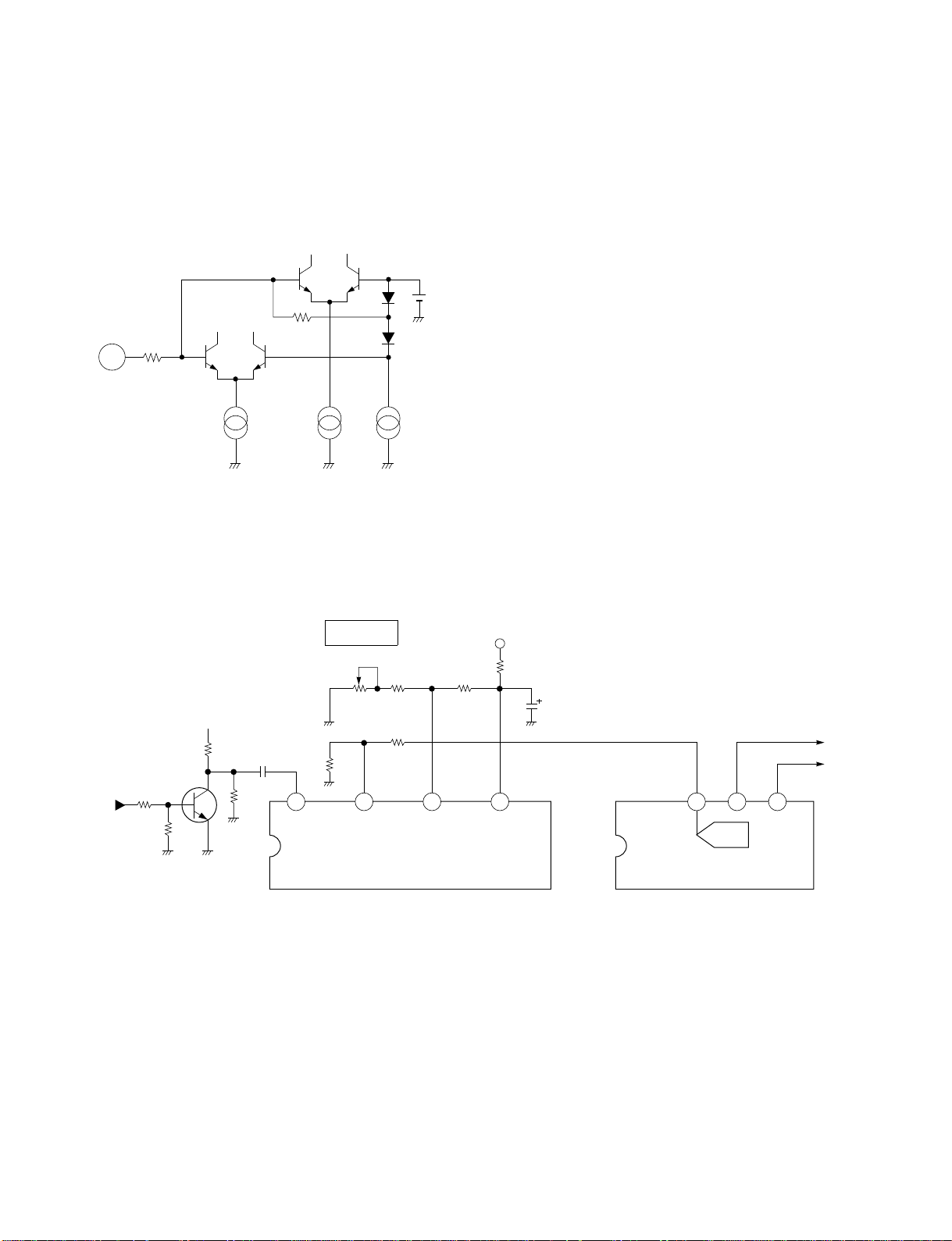
(30) Pin 30 is an input terminal of vertical sync signal.
fH ADJ
R4019
R4015
22K
+12V
14
+9V
8
3
1
R4017
8.2K
Q421
H. sync
signal
Q420 LA7860
Q302 TA1241
DAC
17 14 13
MICROCOMPUTER
I C bus
2
Vertical sync signal of approx. 2 V(p-p) is applied
through coupling capacitor 1 mF.
For input sync signal, both polarities of positive and
negative can be acceptable, and the sync is triggered
at front edge of sync signal.
3.0V
50k
300
30
Fig. 8-32
2-2. Horizontal Phase Shift Circuit
The function to change the horizontal sync signal phase is
also provided for the up-con verter circuit. Howe ver , in fact,
the function is not used in manufacturing adjustment with
the phase change data determined in designing entered.
When performing the phase adjustment (screen position)
in manufacturing, the phase shift circuit built-in LA7860
is used. As previously stated, the DC voltage added to pin
3 can control its phase. The DC voltage is supplied from a
D/A converter built-in E/W IC (TA1241).
The main components of this circuit are shown in Fig. 8-
33. The output voltage of D/A converter is controlled by
the channel selection microprocessor through I2C bus line.
The horizontal phase (screen position) adjustment is carried out by using a remote controller in manufacturing.
Fig 8-33 Horizontal phase shift circuit
8-14
Page 83

SECTION IX
VERTICAL OUTPUT CIRCUIT
9-1
Page 84

1. OUTLINE
The vertical output circuit of this model has the same components as that of usual PJTV except for a kind of E/W IC
(Q302: TA1241). As can be seen from the block diagram,
the sync circuit and the vertical oscillation circuit are contained in Q420 (LA7860), and the sawtooth generation
circuit and amplifier (vertical drive circuit) contained in
Q302 (TA1241). The output circuit and pump-up circuit
are included in Q301 (LA7833).
Q420 LA7860
V. OSC.
Q308
Fig. 9-1 Vertical deflection circuit block diagram
1-1. Theory of Operation
The purpose of the vertical output circuit is to provide a
sawtooth wave signal with good linearity in vertical period to the deflection yoke.
When a switch S is opened, an electric charge charged up
to a reference voltage VP discharges in an constant current rate, and a reference sawtooth voltage generates at
point (a).
Q302 TA1241
SAM TOOTH
WAVE GAIN
CIRCUIT
AMP
LOGIC
CIRCUIT
Q301 LA7833
PUMP-UP
CIRCUIT
OUTPUT
Microcomputer
DEFLECTION
This voltage is applied to (+) input (non-inverted input) of
an differential amplifier, A. As the amplification factor of
A is sufficiently high, a deflection current flows so that
the voltage V2 at point (c) becomes equal to the voltage at
point (a).
YOKE
Vp
(a)
V1
S: Switch
R1 C2 R2
Differential
amplifier
A
L
C2
R3
c
(
)
V2
Fig. 9-2
9-2
Page 85
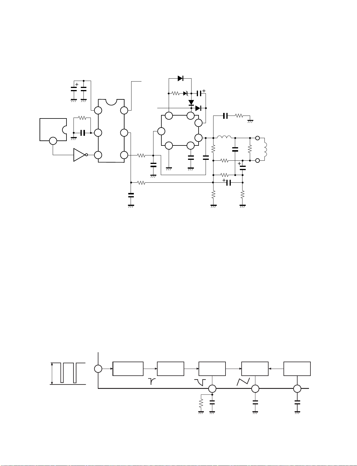
2. V OUTPUT CIRCUIT
2-1. Actual Circuit
Q420
24
C322
R329
C325
Q308
C321
+9V
R308
23
22
21
Q302
6
7
9
C319
+35V
R301
C314
R330
D309
C308
D310
D308
7
4
1
6
Q301
5
C309
3
2
C311
D301
C313
L301 R309
R307
R306
R313
C305
R304
R303
C307
L462+L463+L464
C306
R305
Fig. 9-3
2-2. Sawtooth Waveform Generation
2-2-1. Circuit Operation
The sawtooth waveform generation circuit consists of as
shown in Fig. 9-4. When a trigger pulse enters pin 21, it is
differentiated in the waveform shape circuit and only the
falling part is detected by the trigger detection circuit, to
the waveform generation circuit is not susceptible to variations of input pulse width.
5Vp
DC=0V
21
W AVEFORM
SHAPE
TRIG G ER
DET.
The pulse generation circuit also works to fix the vertical
ramp voltage at a reference voltage when the trigger pulse
enters, so it can prevent the sawtooth wave start voltage
from variations by horizontal components, thus improving interlacing characteristics.
PULSE
WIDTH
22
R 3 2 9 C 3 2 5 C 3 2 2 C 3 2 3
V. R AM P
23 24
+
Fig. 9-4
AGC
9-3
Page 86

2-3. Vertical Output
2-3-1. Circuit Operation
The vertical output circuit consists of a vertical driver circuit Q302, Pump-up circuit and output circuit Q301, and
external circuit components.
(1) Q2 amplifies its input fed from pin 4 of Q301, Q3,
Q4 output stage connected in a SEPP amplifies the
current and supplies a sawtooth waveform current to
a deflection yoke.
Q301
+35V
D301 C308
D308
36
Q3
7
Q3 turns on for first half of the scanning period and
allows a positive current to flow into the deflection
yoke (Q3 ® DY ® C306 ® R305 ® GND), and Q4
turns on for last half of the scanning period and allows a negative current to flow into the deflection
yoke (R305 ® C306 ® DY ® Q4). These operations are shown in Fig. 9-5.
V 3
D309 R308
V 7
60V
36V
GND
36V
BIAS
Q2
4
1
CIRCUIT
Q4
Fig. 9-5 Vertical output circuit
(2) In Fig. 9-6 (a), the power Vcc is expressed as a fixed
level, and the positive and negative current flowing
into the deflection yoke is a current (d) = current (b)
+ (c) in Fig. 9-6, and the emitter voltage of Q3 and
Q4 is expressed as (e).
Power Vcc
Q3
i1
Vce 1
V 2
2
DY
+
C306
R305
Q3 ON
Q4 ON
(3) Q3 collector loss is i1 x Vce1 and the value is equal
to multiplication of Fig. 9-6 (b) and slanted section
of Fig. 9-6 (e), and Q4 collector loss is equal to multiplication of Fig. 9-6 (c) and dotted section of Fig.
9-6 (e).
GND (b) Q3 Collector current i1
GND (c) Q4 Collector current i2
GND
60V
GND
GND
Q2
Q4
i2
(a) Basic circuit
Fig. 9-6 Output stage operation waveform
9-4
GND (d) Deflection yoke current i1+i2
Vp
Vcc
1/2 Vcc
GND
(e)
Page 87

(4) To decrease the collector loss of Q3, the power sup-
y
ply voltage is decreased during scanning period as
shown in Fig. 9-7, and V
decreases and the col-
CE1
lector loss of Q3 also decreases.
Q3 Collector loss decreases
by amount of this area
Power supply
for flyback period (Vp)
Power supply
for scanning period
(Vcc)
Scanning period
back period
Fl
Fig. 9-7 Output stage power supply voltage
(5) In this way, the circuit which switches power supply
circuit during scanning period and flyback period is
called a pump-up circuit.
The purpose of the pump-up circuit is to return the
deflection yoke current rapidly for a short period
(within the flyback period) by applying a high voltage for the flyback period. The basic operation is
shown in Fig. 9-8.
(6) Since pin 7 of a transistor switch inside Q301 is con-
nected to the ground for the scanning period, the
power supply (pin 3) of the output stage shows a voltage of (V
age of (V
– VF ), and C308 is charged up to a volt-
CC
– VF – VZ – VR) for this period.
CC
(7) First half of flyback period
Current flows into L462 ® D1 ® C308 ® D308 ®
VCC (+35V) ® GND ® R305 ® C306 ® L462 +
L463 + L464 in this order, and the voltage across
these is:
VP = V
+ VF + (V
CC
– VF – VR) + VF about 60V is
CC
applied to pin 2. In this case, D301 is cut off.
(8) Last half of flyback period
Current flows into VCC ® switch D309 ® C308 ®
Q301 (pin 3) ® Q3 ® L462 + L463 + L464 ® C306
® R305 in this order, and a voltage of VP = V
VCE (sat) – VF + (V
– VF – VR) – VCE (sat), about
CC
CC
54V is applied to pin 2.
(9) In this way, a power supply voltage of about 36V is
applied to the output stage for the scanning period
and about 60V for flyback period.
–
Q301
D301 C308
D308
6
Q3
Q4
(a) Scanning period (b) Flyback period
3
D309
Switch
7
D1
L462+L463+L464
2
D310
R308
+
C306
R305
Q301
Q3
Q4
D301 C308
6
D1
Fig. 9-8
D308
3
D309
Switch
7
L462+L463+L464
2
Last half
D310
VZ
R308
VR
First half
+
C306
R305
9-5
Page 88

2-4. Vertical Linearity Characteristic
Correction
2-4-1. S-character Correction
A parabola component developed across C306 is integrated
by R306 and C305, and the voltage is applied to pin 7 of
Q302 to perform S-character correction.
2-4-2. Up-and Downward Linearity Balance
A voltage developed at pin 2 of Q301 is divided with resistors R307 and R303, and the voltage is applied to pin 7
of Q301 to improve the linearity balance characteristic.
Moreover, the S-character correction and up & downward
balance correction are performed through the bus control.
Vcc
+36V
R321
R322
Q304
Q301
2-5. Centering Circuit
The centering circuit shown in Fig. 9-9 is only used for
the wide model. In the zoom mode of the wide model, the
function to move the screen position up and down so as
not to hide the characters is required, when the closed caption signal is received.
To move the screen position, as described in the horizontal oscillation circuit, it is necessary to delay the phase of
the vertical sync signal by using the up-converter function.
However, to lower the screen position, it is impossible to
proceed the phase of sync signal. To solve the problem,
after turning on Q305 and Q304, lower the whole raster at
first by flowing the DC current to V
Q304 ® DY ® Q301.
From this status, the screen position is moved up and down
by varying the sync signal delay amount.
The voltage to control Q305 and Q304 on/off is supplied
from pin 7 of Q350 (I/O expander). The voltage at pin 7 is
switched to either high or low through I2C bus line by the
the channel selection microcomputer. In the zoom mode,
the voltage at pin 7 develops high level, and Q304 and
Q305 turn on.
® R321•R322 ®
CC
C306
R305
DY
Fig. 9-9
Q305
Q350
JLC1562BN
7
9-6
Page 89
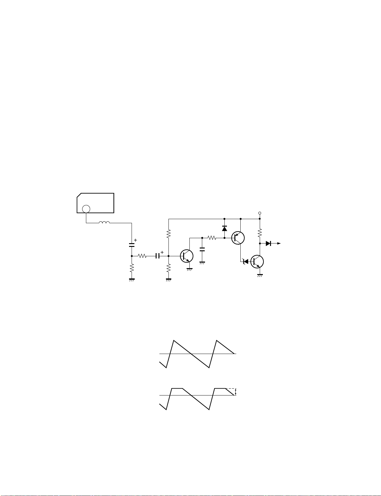
3. PROTECTION CIRCUIT FOR VERTICAL DEFLECTION STOP
V
When the deflection current is not supplied to the deflection coils, one horizontal line appears on the screen. If
this condition is not continued for a long time, no trouble
will occur in a conventional TV. But in the projection TV,
all the electron beams are directly concentrated at the fluorescent screen because of no shadow mask used, and burns
out the screen instantly.
To prevent this, the stop of the vertical deflection is detected when the horizontal one line occurs, and the video
signals are blanked out so that the electron beams are not
emitted.
When the vertical deflection circuit is operating normally,
a sawtooth wave v oltage is obtained across (R305), so Q384
repeats on-off operation in cycle of vertical sync.
2
L462+L463+L464
R305
C306
R382
R383
Q384
C387
R384
In this case, the collector voltage of Q385 is set to (12V –
V
(Q385)) with R386 and C388 as shown in Fig. 9-
CEsat
10. Accordingly, Q385 and Q386 are continuously turned
on. As a result, diode D382 is turned off , giving no influence on the blanking operation.
Next, when the vertical deflection stops, the voltage across
(R305) does not develop, so Q384 turns off, and both the
Q385 and Q386 are turned off. Then, the picture blanking
terminal pin 25 of Q501 is set to high through R387 and
D382 connected to 12V power line, BLANKING CIRCUIT
ON thus cutting off the projection tubes.
+12V
D380
R386
C388
Q385
D381
R387
D382
Q386
BLANKING
CIRCUIT
Fig. 9-10
oltage Across
R305
Q384 V
Q384 BASE
Fig. 9-11
BE
9-7
Page 90

3-1. +35V Over Current Protection Circuit
The over current protection circuit cuts off the power supply relay when it detects abnormal current increased in
the +35V power line due to failure of the vertical deflection circuit.
3-1-1. Theory of Operation
Fig. 9-12 shows the circuit diagram of the over current
protection circuit. When the load current of the +35V line
increases, the voltage across a resistor of R370 will also
increase. When the voltage increases across R370 and the
voltage developed across R371 becomes higher than the
VBE of Q370, Q370 turns on and a voltage de velops across
R374 due to the collector current flowing. When this voltage increases to a value higher than about 1.3V, SCR•D846
operates, thus cutting off the power relay. When the circuit operates, a power LED provided will turn on and off
in red.
Power
Circuit
R370
35V
R371
C370
+
Q370
R373
R374 C371
Fig. 9-12
V. Output
Circuit
R372
D370
To Gate
+
of SCRD846
9-8
Page 91

SECTION X
HORIZONTAL DEFLECTION CIRCUIT
10-1
Page 92

1. OUTLINE
2. HIGH VO LT AGE CIRCUIT
A normal PJTV uses one circuit which realizes two
functions: one flows a deflection current in the deflection
yoke and the second applies a high voltage to the anode of
CRT. However, in this model, these two functions are
separated and realized in two circuits, so that the high
voltage regulation is improved to apply high voltage to
CRT to improved the focus as well as improving the size
regulation. Hereinafter, the former is called DEFLECTION
CIRCUIT, and the latter HIGH VOLTAGE CIRCUIT. The
basic operation principle of these circuits is the same as a
normal TV circuit. HIGH VOLTAGE CIRCUIT is
explained first.
Q416
C408 C407 C404
L461
Fig. 10-1 shows the block diagram.
T461
FBT
1
To
Focus
pack
+148V
Q436
Q435
14
R466
2
ABL
Q437
H. V. AD J
8
Z450
-
13
+
12
1
Q437
+12V
+
-
2
+
3
+
Fig. 10-1 Block Diagram of HIGH VOLTAGE CIRCUIT
To
CRT
Anode
10-2
Page 93

2-1. General
o
2-2. X-ray Protection Circuit
L461 is a choke coil which corresponds to an deflection
yoke in a normal TV. A flyback pulse is generated in the
primary side of FBT and it is booted with a transformer.
This operation is entirely the same as that of a normal TV
circuit. So the explanation of this operation is omitted.
Only the difference is that the voltage to be applied to pin
2 of FBT is controlled with the series regulator of Q435,
Q436, Q437. This series regulator is used to form a high
voltage regulator. The regulator detects the high voltage
output of FBT by dividing it with a resistor, controls the
detected voltage (at pin 12 of Q437) to be constant, and
holds the high voltage at a constant value (31 kV).
Overcontrol may result in an excessive peak power when
a white belt appears. So the AC gain of the error amplifier
is considerably lowered. Therefore, a slight voltage ripple
occurs in the high voltage. Distortion accompanying the
ripple is corrected in the DEFLECTION CIRCUIT. Pins
12 to 14 of Q437 operational amplifier work as a buffer
amplifier, and pins 1 to 3 as an error amplifier of the
regulator.
This circuit prevents dangerous radiation of X-ray from
the CRT when the v olta ge created with FBT is abnormally
increased due to a failure in any part. Fig. 10-2 shows the
block diagram of this circuit.
If the voltage generated in FBT abnormally increases, a
pulse that is generated in other winding of FBT also
increases. To prevent this, the pulse that is generated in
the winding between pins 4 and 9 is peak rectified, so that
the protection circuit works when this voltage increases
over a prescribed level. D471 rectifies the pulse, C471
smoothes it, and R451/R452/R453 divide the voltage and
apply it to the emitter of Q430. If the emitter voltage
increases higher than the value obtained by adding the
zener diode of D472 to VBE of Q430, Q430 turns on and
Q429 also turns on. When Q429 turns on, a voltage is
applied to the gate of SCR/D846 which forms the
protection circuit of the power supply circuit and the SCR
turns on. When the SCR turns on, the relay of the power
supply circuit opens, the AC current is not supplied to the
switching power supply and the set stops operation. This
state is held until the AC power cord plug is disconnected.
When the AC plug is disconnected and the 5V – 1 for the
channel selection circuit is sufficiently lowered, the SCR
is turned off and restored. In addition, the vertical output
circuit, the converter output circuit and the main B line
overcurrent protection circuit are connected to the gate of
the SCR.
To GATE
f SCRD846
D473
Q429
+
+12V
Q430
D472
X-1 R-1
R451
R452
R453
Q416
+
C471
D471
T461
FBT
9
4
1
2
Fig. 10-2 X-ray protection circuit block diagram
10-3
Page 94

2-3. 200V Low Voltage Protection Circuit
Fig. 10-3 shows a block diagram of this circuit.
The 200V line power taken from the FBT is supplied to
the video output circuit of the CRT-D unit. If this voltage
decreases, the CRT cathode v oltage lowers and an excessi ve
cathode current flows out causing a damage in the CRT.
To prevent this, the protection circuit is provided so that
when the 200V drops, the set stops operation. As sho wn in
Fig. 10-3, the 200V line voltage is divided with a resistor
and is applied to pin 10 of IC (Q302). The pin 10 is
internally connected to the comparator’s input terminal.
+149V
D406
3
5
T461
FBT
+
C496
The other input terminal of the comparator is supplied with
a reference voltage of 6.25V. If the voltage at the pin 10
drops to lower than 6.25V, it is judged occurrence of any
error. The result of this judgment is read with the tuning
microcomputer through the I2C bus. The microcomputer
turns off the power and turns on and of f the red LED flicker
on the front of the set. Unlike when the power supply
protection circuit D846 (described above) turns on, the set
resumes operation by turning the power on through a
remote controller.
CRT - D UNIT
210V
R417
220K
158
159
1
2
Video
out
To
MICROCOMPUTER
R418
180K
+
R327
18K
2
I C BUS
14
15
6.25V
Q302
TA1241
10
Fig. 10-3 200V low voltage protection circuit bloc k diagram
10-4
Page 95

3. DEFLECTION CIRCUIT
Fig. 10-4 shows the primary circuits.
AFC PULSE
T462
3
1
11
149V
Q436
Q439
1
Q440
Q404
C406C405
+
-
2
+
3
Q440
7
C487 R486
+12V
5
+
-
6
R353
DY
L441
C428
8
+9V
Q302 TA1241
+
EHT
E/W
FB
VCC
2 3 5 6
Q303
7
Q437
T461
-
9
10
+12V
-
5
+
6
8
+
Q437
Q437
-
H. V.
ADJ
13
+
12
14
FBT
Z450
To
CRT
Fig. 10-4 Deflection circuit diagram
10-5
Page 96

3-1. General
T462 in Fig. 10-4 is a transformer which corresponds to
FBT in a normal TV circuit. However, in this model, an
AFC pulse is taken from this transformer and is applied to
the horizontal oscillation circuit and V/C/D IC. Like the
high voltage circuit, the basic operation is the same as
that of a normal TV circuit, and the explanation is omitted.
Only the difference is that the series regulator is used to
control the horizontal width and to correct E/W distortion.
This series regulator comprises Q436, Q439 and Q440.
The horizontal width and E/W distortion correction voltage
is controlled by the voltage at pin 3 of E/W IC Q302
through Q303 and R353. The voltage generated at the pin
3 is controlled with the channel selection microcomputer
through the I2C bus. Therefore, the horizontal width and
E/W distortion can be adjusted by using a remote controller,
for example. Complete correction of the E/W distortion
causes excessive loss in the series regulator. So it is
corrected 50%, and another 50% is corrected with the
digital convergence. Therefore, for the E/W distortion
adjustment data, the value determined when designing is
entered and adjustment for each set is not made in the
production process. In addition to the horizontal width and
E/W distortion control voltage (described above), a v oltage
to correct distortion such as WPD caused by a high voltage
ripple is also applied to the pin 6 of the ope. amplifier
Q440. The high voltage ripple waveform is reverse
amplified and is supplied from the pin 7 of the ope.
amplifier Q437 through R486 and C487. The waveform
obtained by amplifying the high voltage ripple is applied
also to the EHT terminal (pin 2) of E/W IC Q302. This
controls the vertical width and corrects a change in the
vertical width caused by the high voltage ripple. The dr ive
circuit uses an FET. The scanning frequency is as high as
31.5 kHz. If the storage time is different, the drive pulse
duty ratio largely changes and the horizontal out loss
increases. This is the same for the high voltage circuit. A
push-pull predrive circuit is provide to drive the FET. The
operation principle is the same as a normal PJTV, except
the transistor.
3-2. S-character Capacitor Switching
As the circularity at the center of the screen is set high in
the theater mode of the wide model, the horizontal linearity
is set so that the center of the screen shrinks and both ends
expand. To realize this horizontal linearity, the switching
circuit which increases the S-shaped capacitor capacity is
added in the theater mode of the wide model.
Fig. 10-5 shows the block diagram of this switching circuit.
When the theater wide mode is selected, Q491 and Q490
turn on and the relay SR41 closes. In addition to C428 and
C429 which have been connected, C491 is connected in
parallel to increase the capacity. At this time, C411 is
connected in parallel to C412. C411 is a capacitor of the
dynamic focus circuit. As the S-shaped capacitor increases
in capacity, the parabolic voltage generated at both ends
becomes small and the dynamic focus voltage amplitude
becomes small. With the capacity increased, the voltage
applied to the primary winding of the focus transformer is
increases to adjust the dynamic focus amplitude. The
voltage to turn on Q491 is supplied from the pin 6 of the I/
O expander Q350. Q350 is controlled with the tuning
microcomputer through the I2C bus line. Since the
horizontal linearity is changed as described above, the f inal
linearity is determined by adjusting the digital conver gence
though the S-shaped capacitor is switched. In PJTV,
regardless of the display mode, the horizontal or vertical
linearity is finally determined by adjusting the digital
convergence.
3-3. Horizontal Stop Protection circuit
As the high voltage circuit continues operation even if the
deflection circuit fails and stops, a vertical line remains
on the screen burning the CRT fluorescent surface. To
prevent this, a protection circuit is provided to stop the
whole set when the deflection circuit fails and stops. Fig.
10-6 shows this circuit. The protection circuit detects the
AFC pulse of the transformer T462 which corresponds to
an FBT. Rectifying the AFC pulse with D451, it generates
an DC voltage.
The voltage is approximately 65V when the set is normal.
Dividing the voltage with R490 and R492 and applying to
Q451, a voltage of about 11.0V can be obtained at the
emitter of Q452. Q452 turns on, the voltage at the collector
of Q452 drops to 3.5V the same voltage at the emitter, and
the zener diodes D454 and D456 turn off. This is the
operation flow in a normal state. If any error occurs and
the AFC pulse becomes small, Q452 turns off and the
voltage at its collector rises to 12V. Then, D454 and D456
turn on and blank the video signal, and at the same time
they actuate the protection circuit of the power supply
circuit stopping the set. The circuit of Q441, D440 and
C450 prevents a malfunction when the above protection
circuit turns on the power switch. When the protection
circuit turns on the power switch, a char ging cur rent flows
from C450 to Q441 and Q441 turns on grounding the anode
of D454.
10-6
Page 97

Therefore, the power supply protection circuit does not
k
work. The protection circuit explained above is effective
also when the winding of pins 3 and 1 of T462 are shorted,
preventing T462 from bur ning. Another protection circuit
which has the same configuration as that of Q451 and Q452
is connected to the pin 6 of the transformer T462. This
protection circuit comprising Q431 and Q432 detects the
pulse that is smaller than the pulse, and the resistance value
is different accordingly. This protection circuit also works
when the pulse becomes small, but the main purpose is to
protect the transformer from burning when the winding of
T462 is shorted.
Q404
DY
L441
When the windings between the pins 6 and 5 and between
the pins 4 and 5 are shorted, this protection circuit works.
These windings are not used at all, and an unnecessary
winding exists because the existing transformer is used.
The transformer burns when the secondary winding is
shorted. Because, as the turn number of the secondary
winding is small, combining with the primary winding is
weak, and influence of the short-circuit does not almost
appear in the primary side and the operation continues as
normal. This makes a large current flow in the secondary
winding. As a result, the secondary winding is heated and
burnt.
T462
11
8
C428C429
Q490
C491
C411
SR41
T411
2
512
C412
9
Q491
Q302 JLC1562BN
To Focus Pac
6
Fig. 10-5 S character capacitor switching circuit
10-7
Page 98

Q 404
T462
11
AFC pulse
D451
R490
6.2K
4
5
6
R492
1.2K
Q 451
Q 452
D453
UZ3.0
+12V
C450
D440
UZ7.5
D456
UZ7.5
D454
+
D452
D439
Q 441
Blanking
circu it
To GATE
SCRD 846
8
3
1
+
C466
Fig. 10-6 Protection Circuit diagram
10-8
Page 99

3-4. CRT Protection Circuit
This circuit stops operation of the spot killer circuit to
prevent the CRT fluorescent surface from burning when
the vertical circuit or deflection circuit fails. The spot killer
circuit operation is explained first. If the anode voltage is
held high after the power supply is turned off, the CRT
surface may bright as a spot because of radiation of electron
from dust in the CRT even if no signal is applied to other
electrode. To prevent this, a large anode current is made
run at the moment when the power is turned off, so that
the high voltage applied to the anode electrode is decreased
as far as possible. The circuit called a spot killer performs
this function.
The spot killer circuit comprises C965 and Q967 in this
block diagram. C965 and C966 are charged, so that while
the power is being supplied, the voltage at both ends of
C966 is Vf. Therefore, Q967 is held off. When the power
is turned off, the 9V power supply voltage begins to
decrease, and the emitter voltage of Q967 is also decreased
by the voltage charged at both ends of C965. When Q967
turns on, a current is taken out from the emitter of the
transistor in the upper stage of the video output circuit
that is connected in cascade.
As a result, the cathode voltage of CRT suddenly drops, a
large cathode current flows, and the high voltage is
decreased. Therefore, if an error which cause stop of a
deflection current and the protection circuit of the power
supply circuit works to stop operation of the set, the spot
killer circuit works and the fluorescent surface of the CRT
is burnt due to the large cathode current. This occurs often
if the 35V overcurrent protection circuit of the vertical
output circuit or the horizontal stop protection circuit
works. So, when the protection circuit of the power supply
circuit works, the spot killer circuit is made ineffective to
protect the CRT. The circuit comprising Q483 and Q4 in
Fig. 10-7 is the CRT protection circuit. When a trigger is
applied to the gate of the SCR D846 used in the protection
circuit of the power supply circuit, Q483 also turns on at
the same time. Q484 also turns on and runs the current
toward C965 of the spot killer circuit to prev ent the emitter
voltage of Q967 from being dropped and Q967 from being
turned on.
Main B
Overcurrent
protection circuit
35V LINE
Overcurrent
protection circuit
Hor. stop
Protection circuit
X -Ray
Protection circuit
12V
Q484 D483
Q483
To GATE
SCRD846
162 5
9V
2200 µF
C965
C966
0.47 µF
CRT-D UNIT
+
+
Q967
CRT
Fig. 10-7 CRT Protection Circuit
10-9
Page 100

This page is not printed.
10-10
 Loading...