

Page 1
Page 2

FOREWORD
The material presented in this manual is provided for the technical training of TACP employees
and qualified service personnel only.
This manual is intended as a supplement to the Toshiba Service Training Manual, " Servicing the
N5SS Color Television Chassis/Digital Convergence", File Number NTDPJTV04. This manual
concentrates on the changes in the Video and Audio signal paths, with additional information on
troubleshooting power supply shut down circuits.
The specific circuit reference designations, pin numbers, etc., are taken from the TP50G60/
TP55G60 Service Manual, File Number 020-9711. The diagrams in this manual are simplified for
training and should be used as a reference guide only when servicing the N7SS PJTV Chassis. Refer
to the applicable service data for detailed adjustment and servicing procedures.
NTDPJTV07
SERVICING TOSHIBA'S N7SS TELEVISION CHASSIS
©1997
TOSHIBA AMERICA CONSUMER PRODUCTS, INC.
National Service Division
National Training Department
1420B Toshiba Drive
Lebanon, TN 37087
(615) 449-2360
No part of this manual may be reproduced in whole or in part without prior written consent from
Toshiba America Consumer Products, Inc., Service Division.
Page 3

Contents
Section 1
Video Signal Flow
1-1. Basic N5SS and N7SS Differences........................................3
1-2. Video Signal Flow..................................................................3
Section 2
Audio Signal Flow
2-1. Audio Signal Flow..................................................................7
Section 3
Power Supply
3-1. Outline of system................................................................10
3-2. Standby Power Supply.......................................................11
3-3. Main Supply........................................................................11
3-4. Outline of the Current Resonant Type Supply.................12
3-5. Fundamental Theory of LC Series Resonant Circuit......12
3-6. Main Supply Actual operation.........................................13
3-7. Scan derived voltages (FBT)..............................................17
3-8. Protector Module (Z801)...................................................18
3-9. Sub Supply..........................................................................19
Section 4
Shut Down Circuits
4-1. Summary of Shut down circuits.........................................21
4-2. Power shut down troubleshooting guide...........................23
4-2-1. +30 Volt Over Voltage Protect....................................................... 24
4-2-2. +15V Over Voltage Protect.............................................................24
4-2-3. +30 V Over Current Protect...........................................................25
4-2-4. +15V Over Current Protect............................................................25
4-2-5. -15V Over Current Protect.............................................................26
4-2-6. +35V Over Current Protect............................................................26
4-2-7. +/-15V Under Voltage Protect.........................................................27
4-2-8. 200V Under Voltage Protect...........................................................28
4-2-9. X-Ray (High Voltage) Protect.........................................................28
4-2-10. +125V Over Current Protect........................................................29
1 JRS 12-97
Page 4

Section 1
Video Signal Flow
2 JRS 12-97
Page 5

1-1.Basic N5SS and N7SS Differences
The basic operation of the standard aspect ratio, interlace scan N7SS version of the TG-1 chassis is similar to
the N5SS version. In the E - series N5SS, the microcomputer generated the OSD, but in the N7SS, the new
OSD board generates the On Screen Display, as well as
the EDS and Closed Captioning. The On Screen Display is now Icon based and much more user friendly.
Some Projection models include a component video
input, known as"Color Stream", for use with a DVD
player.
Dolby ProLogic audio and StarSight have been
removed from most models.
The power supplies are mostly the same as in the
N5SS. Some models contain a new version of the
main supply voltage control IC, Q801.
The Theater Wide models and the Progressive Scan
models are not addressed in this update.
Although this treatment focuses on the TP50G60, the
video and audio signal flow diagrams can be applied
to most standard, interlace scan TG-1 chassis.
1-2. Video Signal Flow
Figures 1and 2 illustrate the video signal flow through
the chassis. The Antenna 1 (ANT 1) and Antenna 2
(ANT 2) inputs allow two separate RF signals to be connected to the RF switcher. When the switch, controlled
by the microcomputer, QA01, is in the up position, the
ANT 1 signal is connected to the HY01 PIP Tuner/IF
and the H001 Main Tuner. Moving the switch down
connects the ANT 2 signal to the H001 Tuner. Due to
the RF Switch, the ANT 2 signal can’t be used as the
PIP source, but when ANT 2 is selected the ANT 1 signal is available at the RF OUT. The PIP Tuner/IF produces a composite video (CV) signal and sends it to the
AV Switcher , QV01. An IF signal produced by the Main
Tuner is sent to H002, which produces a composite video
signal and sends it to the AV Switcher.
A switch on the Cb jack of the video 2 input tells the
Switching IC, QV01, when a composit video input is
connected to video 2. This will will result in different
switching in the signal path.
When the input to video 2 is component video, the following path does NOT apply.
The selected video signal is output as composite video,
and sent to the video output jack, the New OSD Board,
and the Digital Comb Filter. After Y/C seperation, the
video signal is sent back to the AV Switcher as separate
luminance (Y) and chrominance (C) signals. The Y and
C signals are then sent to Q501, the Video Chroma Deflection Processing IC. Q501 processes the video signal and sends separate Y, I, and Q signals. The Y, I, and
Q signals are then sent to QW01, the Color Switch.
Component video from video 2 input can now be considered. The video 2Y, Cr, and Cb signals are also sent
to QW01. This circuit switches the video source for the
Y, I, and Q signals for the main picture input to Q501.
Q501 processes the selected signals into seperate R, G,
and B. The R, G, and B signals are sent to the CRT
drives and the CRTs.
If the PIP feature is selected, composite video from AV
Switcher is sent to the PIP circuit, ZY01. After processing, the PIP signal is sent to Q501 as R, G, B, and YS
where it is mixed with the main video. NOTE: When
component video is connected to video 2, video 2 can
not be used as a PIP source.
RGB signals from the digital convergence board are sent
to the Q501 via the PIP board, ZY01.
On screen display (OSD), Extended Data Service (EDS),
and Closed Caption (CC) data RGB is generated on the
New OSD board, UM01. These signals are applied to
Q501, where they are mixed with the main and PIP video
signals.
Three video inputs, video 1 through 3, are applied to the
AV Switcher . The video 1 input can be composite video,
Y/C video, or the test signal from QA01. Video 2 can
be composite video or component video, and video 3 is
either composite video or Y/C video. A mechanical
switch on the video 1 input defaults to the test signal, so
a video connector must not be plugged into the video 1
input jack when the internal test signals are to be used.
3 JRS 12-97
Page 6
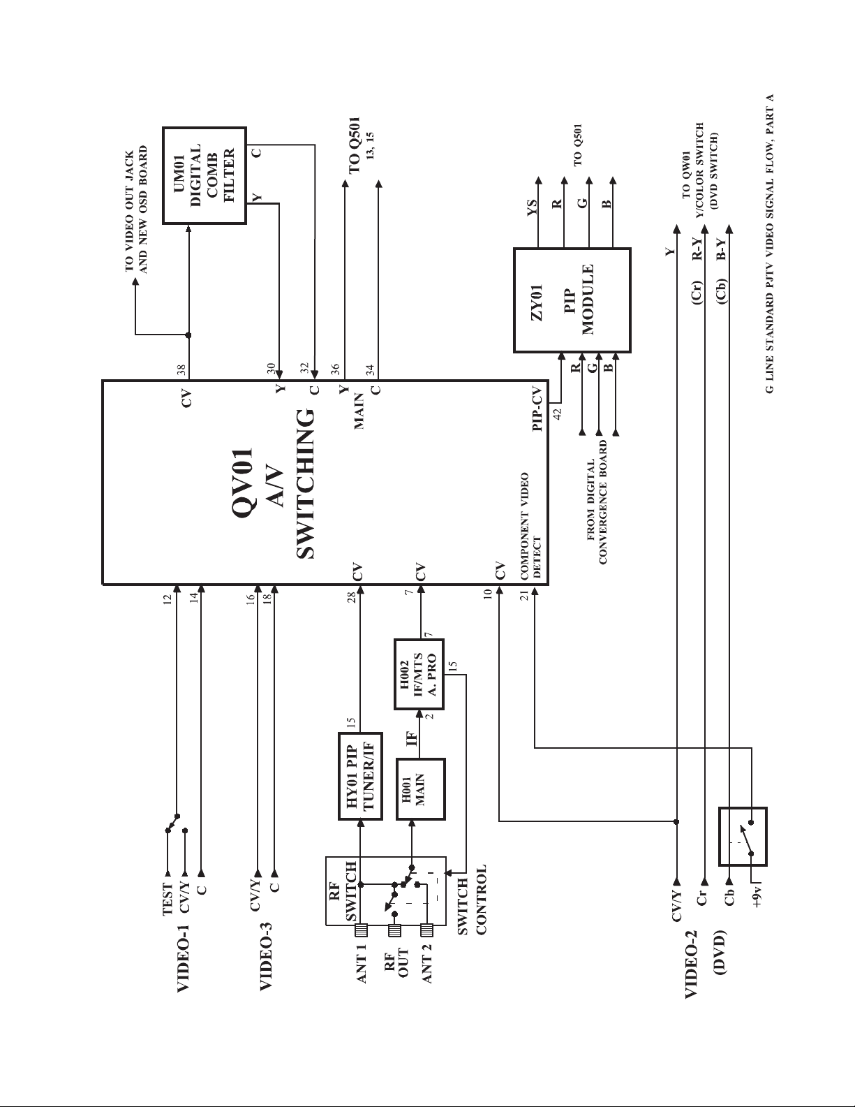
Figure 1. Video Block A
4 JRS 12-97
Page 7
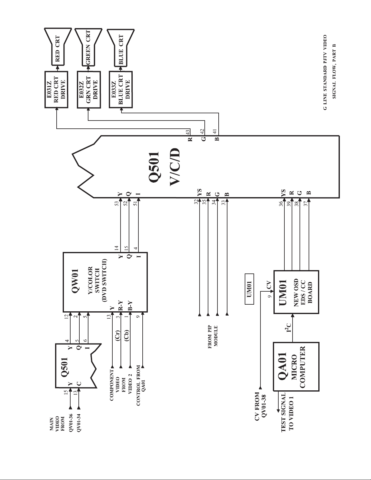
Figure 2. Video Block B
5 JRS 12-97
Page 8

Section 2
Audio Signal Flow
6 JRS 12-97
Page 9

2-1. Audio Signal Flow
Figure 3 illustrates the audio signal flow.
L and R Audio signals are applied to the AV Switcher
from the Video 1, 2, and 3 audio jacks, and the IF/MTS/
A. PRO IC, H002. There is no PIP tuner audio. Like
the video signal, there must not be a connector in video
1's audio jacks for the audio test signal to be applied to
the AV Switcher. The main audio signals are applied to
the audio output jacks and to the Front Surround circuit.
After processing, the left and right audio signals are applied to the audio processor in H002 where the volume,
balance, treble, and bass are controlled. Next, the audio
signals are amplified by QS101 and applied to the variable audio output jacks, and to power amplifier, Q601.
If the sub bass system (SBS) is selected, the signal is
mixed with the left and right signals just before Q601 to
increase the bass response.
In the TP50G90, TP55G60, and TP61G60/90models,
jumpersGJ01 and GJ02 are removed, and a center channel switch and audio jack are added to the rear connector panel. A center audio signal from an external source
can be connected here and switched in to replace the
main left and right signals to the internal speakers.
7 JRS 12-97
Page 10
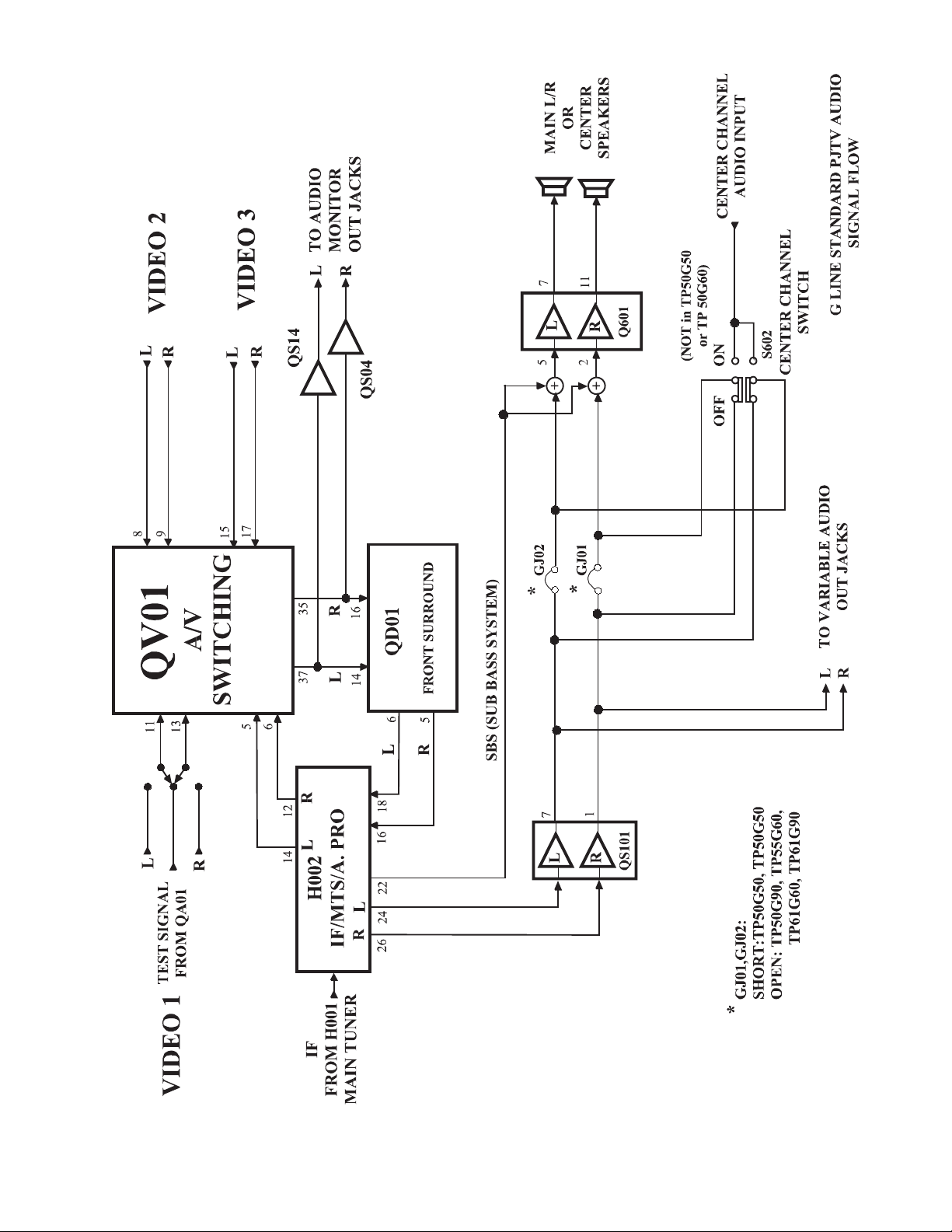
Figure 3. Audio Block
8 JRS 12-97
Page 11

Section 3
Power Supply
9 JRS 12-97
Page 12

3-1. Outline of system
The TP50G60 and TP55G60 power supplies are almost
identical to the E models. The Main Supply utilizes a
new Q801Control IC, the STR-Z4201. The pin outs
are different, but it operates similar to the STR-Z3201.
A Block diagram of the power supply cicuits is shown
in Figure 1. The power supply circuits consist of:
1) Stanby Supply. Supplies the +5V standby power to
the microcomputer and +12V to the ON/OFF relay
(SR81).
2) Main Supply . Supplies Horizontal output B+ (+125V),
Audio output Vcc (+38V), and the Siganl processing
voltages.
3) Sub Supply: Supplies +30V, +15V, and -15V to the
Convergence out board.
Figure 4. Power Supply Block Diagram
10 JRS 12-97
Page 13

3-2. Standby Power Supply
3-3. Main Supply
The standby power supply supplies 12V to close the
relay, SR81 and supplies the 5V and reset 5V to the
microcomputer. T840 supplies a low AC signal to D840.
D840 Rectifies the signal and C840 filters it to produce
12VDC. The 12V is applied to Q840. Q840 regulates
the 5V on pin 5 and supplies the reset at pin 4. Reset
occurs when power is first applied at Q840. The 5V on
pin 5 comes up first while pin 4 stays low. This is the
reset condition. After C843 fully charges, Pin 4 goes to
5V for normal operation.
D801 and C810 is the rectifier and filter for the main
switching supply; they produce 165V . R810 suppresses
rush current at turn on. SR81 is the relay that turns on
the main supply. The relay is controlled by the microcomputer through the relay drivers; QB30 and Q843.
Figure 5. Standby power and Main supply Rectifier
11 JRS 12-97
Page 14

3-4. Outline of the Current Resonant Type
Supply
Fig. 6 shows the configuration for the current resonant
switch mode power supply. The primary side is an LC
series circuit. It consists of the primary winding of the
transformer and a resonant capacitor in series. Two
power MOS FET’s, in a push-pull configuration, drive
the primary side of the transformer.
The switching action on the primary side of the transformer produces the main B+ on the secondary side. The
Figure 6. Basic configuration
main B+ is regulated by negative feedback. The main
B+ is feed into an error amplifier and outputted to a
photo coupler. The output of the photo coupler is applied to the primary side of the power supply to control
the switching speed.
3-5. Fundamental Theory of LC Series
Resonant Circuit
The LC series resonant switch mode power supply is a
frequency regulated power supply operating above resonance. When the the load increases on the secondary
side of the transformer, the frequency decreases (operates closer to resonance) and the current increases.
Conversely, when the load decreases, the frequency increases, and the current decreases.
Figure 8. CharacteristicsFigure 7. LC series resonant circuit
12 JRS 12-97
Page 15

3-6. Main Supply Actual operation
Refer to Figure 9, STR-Z4201 block diagram, and Figure 10, waveforms. Table 1 lists the pin functions.
1. Start-up
When power is applied to the set, a start-up
voltage of 16V is applied to pin 9 of IC Q801. At the
same time, charging of C869 (pin 8) induces a delay to
the internal latch circuit to prevent the Over Voltage
Protect (OVP) circuit from shutting the set down.
2. Output switching element
Two power MOSFETs operating in push-pull
mode are used for switching. The on-off timing of each
is controlled by the logic inside Q801. T o avoid a short
circuit from occuring, a delay is used between the turn
off of one MOSFET to the turn on of the next. (Delay
or Dead Time.)
3. CT (Pin 4) - basic oscillation
The frequency of the internal oscillator is controlled by the Oscillator Control block. The frequency
is determined by the charge and discharge of capacitor
C862 connected to CT terminal. The oscillator generates a ramp waveform at Pin 4. The ramp waveform
charges up to 4 Volts (typical) and discharges to about
2.5 Volts. The charging time is the output-on period,
and discharging time is the off period (see OSC OUT
SIGNAL waveform of Figure 10). The lowest oscillation frequency is determined by capacitor C862 and resistor R867.
5. Css (Pin 7) - soft start
When power is first applied, the switching frequency is set high by capacitor C866, resulting in soft
start of the switching supply. Thus, current sur ge in the
POWER MOSFET output is limited to provide stable
starting of the supply. After initial start-up, the circuit
operates at its nominal frequency of 70-80 kHz.
6. CD (Pin 8) - Latch Delay
The Latch circuit shuts the power supply off
(shut-down) when a fault is detected. Shut-down occurs
by detecting errors from the following:
• Over voltage protection (OVP) circuit
• Thermal shock detection (TSD) circuit
• Over current protection (OCP) circuit
• Loss of and no recovery of Main B+
The charging time of capacitor C869 connected
to the CD terminal (Pin 8) is used to delay the operation
of the Latch circuit when power is initially applied. If
the unit goes into shut-down, temporarily remove ac
power to reset the latch circuit.
7. OC (Pin 11) - Over Current Detect
This is to detect over-current in the LC series
resonant circuit.
8. Over voltage protection (OVP)
If the Vcc terminal (Pin 9) exceeds 22V (typical), the Latch circuit is engaged (shutdown) .
4. CONT (Pin 5) - frequency control
Current flowing out of the CONT terminal (Pin
5) varies the charging current of oscillator capacitor
C862, which in turn controls the frequency of the Output signal (Pin 14). The control current is determined
by the Photocoupler. The Photocoupler phototransister
current is determined by the feedback current of the
photodiode. The photodiode current is determined by
the Error Amp inside of Z801, which is monitoring the
+125V source. Thus, the terminal current (CONT) corresponds to the feedback from the +125V output.
9. Thermal shock detection (TSD)
This is to make the Latch circuit operate when
the IC's internal temperature exceeds 150°C.
13 JRS 12-97
Page 16

Figure 9. STR-Z4201 (Q801)
14 JRS 12-97
Page 17

Figure 10. Waveforms
15 JRS 12-97
Page 18

Pin No. Symbol Function
1VIN Half bridge power input
2 Gnd Ground
3 DT Dead time resistor terminal
4 CT Oscillator capacitor terminal
5 CONT Oscillator control terminal
6FMAX Maximum Frequency determining resistor terminal
7CSS Soft start capacitor terminal
8 CD Capacitor for delay latch: ON-OFF terminal
9VCC Power source terminal for control section
10 DRI VCC Gate Drive power supply output terminal
11 OC Over current detect terminal
12 COM Half bridge GND
14 OUT Half bridge output
15 V
B High side gate drive power source input
Table 1. STR-Z4201Pin function
16 JRS 12-97
Page 19

3-7. Scan derived voltages (FBT)
Figure 11 shows the voltages derived from the FBT of
the Horizontal Deflection circuit. The FBT derives 200V
for the Video Output circuit from pin 3, +35V for the
Fail Safe, H.V. Regulator, Blanking, Dynamic Pin Cushion (DPC), and Vertical Deflection (V .D.) circuits from
pin 6, and -27V for the side DPC circuit from pin 5,
Heater voltage from pin 9, Automatic Frequency Control (AFC) and blanking signal from pin 10, and the
Automatic Black Level (ABL) signal from pin 8.
A 12Vdc source is also derived, via pin 7 and D408, to
supply the SVM and DPC circuit boards. In addition,
the 12Vdc source is used to develop the +9V-1 source
via a 9 V olt regulator made up of Q420, Q421, and D427.
High voltage is supplied from the secondary along with
Focus and Screen voltage sources developed from a tap
on the high voltage secondary of T461.
Figure 11. Scan Derived Voltages
17 JRS 12-97
Page 20

3-8. Protector Module (Z801)
Figure 12 shows the standardized protector module,
Z801. The following are the four sections within the Protector Module: Error Amp, Switch/Latch, B+ OCP, and
X-Ray Protect. In addition the Over Current Protect
(OCP), Over Voltage Protect (OVP), and Under Voltage Protect (UVP) circuits are routed through the internal Switch/Latch circuit to trigger the unit off through
the Protect output (Pin 16).
The Error Amp circuit monitors the B+, 125V line,
via Pin 1. The Error Amp controls the current through
the photodiode of photocoupler Q862. When the B+ voltage decreases, Q862 conducts less, and when it increases, Q862 conducts more.
The Switch/Latch circuit is used to turn off SR81 re-
lay in case of over current, over voltage or under voltage. In shutdown mode, Pin 16 (Protect) latches low,
which turns QB30 off. When QB30 turns off Q843 turns
off. This causes the relay (SR81) to open and thereby
disconnect the power.
In the B+ Over Current Protect (OCP) circuit, the
current is being compared across R470, which is applied
through Pins 1 and 2. The resistance of R470 is so small
that changes in voltage equate to larger changes in current. When a large enough change in voltage occurs, the
internal latch circuit outputs a low on Pin 16, which
shuts the unit down.
In the X-Ray Protect circuit, Pin 11 provides a refer-
ence voltage of +25V. If the High V oltage increases abnormally , Pin 9 of T461 senses the increase and increases
the voltage through R472. This increased voltage is applied to D471, which rectifies AC to DC. The increase
in Vdc is applied to Pin 13, which will trigger the internal latch circuit and output a Low on Pin 16. As long as
+5v-1 is applied to pin15, the remote control hand unit
will not recover the power. The AC power line must be
disconnected to reset the latch.
Figure 12. Protector Module, Z801
18 JRS 12-97
Page 21

3-9. Sub Supply
The Sub Supply is located on the Convergence Out/
Power2 board. Figure 13 shows that the Sub Supply is a
ringing choke converter, using hybrid IC STR57041. Operation begins with a start-up voltage that is applied
through R852. This provides a trickle base current to
Q1 (internal to the IC, Pin 2 of Q802), which causes it
to turn on. When Q1 turns on, the collector current begins to flow . During this start-up time the current is flowing through the primary winding of T888 through Pins 2
and 5. At the same time current will flow through Pins 7
and 8, which create the detection winding, as well as
Pins 8 and 9, which create the base drive winding. During the first half cycle of the AC pulse no current flows
through the detection winding because of the reversed
polarity of D856. Pin 9, however, provides positive feedback for the base, as the electromagnetic inductance increases, to rapidly turn Q1 on. As Q1 becomes saturated the current through the primary winding decreases.
This decrease in current through the primary winding,
reduces the electromagnetic inductance across the base
drive winding, which decreases the voltage to the base
of Q1 and thereby rapidly turns Q1 off.
T888 uses a detection type winding through Pins 7 and
8. The secondary windings are proportional to the detection winding. Subsequently, any fluctuation in voltage across the secondary windings is sensed across the
detection winding which is fed back through Vo sense
(Pin 1). This feedback is used to regulate the On/Off
time of the internal switching transistor Q1.
R846, C845, R852 and D848 create a voltage clamping
circuit that allow the collector voltage of Q1 to stay within
a specified level. R847, C855, R848 and D849 filter the
base voltage. Q850, Q851, Q852, C856, D855, R857
and R859 create the Slow-start circuit. C856 determines
the rate of the start-up time.
Figure 13. Sub Supply
19 JRS 12-97
Page 22

Section 4
Shut Down Circuits
20 JRS 12-97
Page 23

4-1. Summary of Shut down circuits.
Figure 14 is a block diagram of the eleven shut down
circuits. When any of the shut down conditions occur,
the latch in Z801 holds the power relay off as long as the
set is plugged in. Neither the front panel power switch,
nor the remote power switch will restore power to the
set. The front panel power LED will blink at approximately 1/2 second intervals. To reset the shut down condition, the AC main power cord must be unplugged.
Plug the AC cord back in. While listening carefully for
the click of the power relay activating, turn the power
on. If the power relay clicks on, then immediately off,
and the power LED starts blinking, a shut down
condition has occured.
If the relay doesn't energize at all, check the AC input
circuits, fuse F801, and the standby power supply.
If the relay clicks on and the power LED remains on,
the set is not in shut down.
When the set does go into shut down, the problem becomes how to determine which conditioned caused it.
X-ray Protect.
The X-ray protect is connected to pin 13 of Z801. Z801
compares this voltage to the reference voltage on pin 11
(aproximately 25 volts). If the voltage on pin 13 rises to
a value GREATER than pin 11, shut down occurs and
all power drops to zero, except the standby supply.
A peak response meter connected at pin 13 of Z801,
while power is applied to the set, will capture a voltage
greater than the reference voltage, indicating excessive
High Voltage.
+125V Over Current Protect.
The peak hold meter is connected across resistor R470,
and NOT referenced to ground to monitor for a momentary increase in voltage. The normal voltage across R470
is about 0.4Volts. An increase in current will cause the
voltage across R470 to increase. When Z801 detects
this voltage increase, it puts the set into shut down.
Peak Response Meter.
Each shut down circuit has a "Trigger Voltage", which
will cause shut down. The trigger voltage lasts for just a
brief moment before the power supply shuts off. A PeakResponse Meter is required to troubleshoot the shut
down circuits. A peak response meter measures and
holds the highest voltage that occurs at a test point.
Nine circuits are connected to pin 14 of Z801. Each of
these circuits operate in a similar manner. Normally, all
"triggers" are approximately zero volts. When an abnormal condition occurs, the appropriate shut down circuit triggers a "high" to pin 14 of Z801. Z801 sets and
holds pin 16 low (0 volts). This causes relay SR81 to de
energize, dropping all power in the TV, except the
standby power. This means the trigger voltage also drops
to zero. There is now no means to determine which circuit caused the shut down. The only way to reset Z801
is to pull the AC plug.
To determine which cicuit triggered the shut down, connect the peak response meter to each shut down circuit
Trigger monitor point in turn, while applying power to
the set. Any voltage at a monitor point above
aproximately 2 volts is a clear indication that the circuit
being monitored is in shut down, narrowing the search
for the actual fault.
21 JRS 12-97
Page 24

Figure 14. Summary of Shutdown circuits.
22 JRS 12-97
Page 25

4-2. Power shut down troubleshooting
guide.
23 JRS 12-97
Page 26

4-2-1. +30 Volt Over Voltage Protect.
When the supply voltage goes beyond the zener votage,
the zener diode conducts and delivers a voltage to the
anode of D 863. D 863 conducts, a "high" is applied
to pin 14 of Z801, and shut down takes place.
Normal voltage at the monitor point is about 0. A voltage of about 2.5V or greater will result in shut down.
Figure 15. +30V Over Voltage Protect.
4-2-2. +15V Over Voltage Protect.
The +15V over voltage protect operates in a similar fashion as the +30V over votage protect.
Figure 16. +15V Over Voltage Protect.
24 JRS 12-97
Page 27

4-2-3. +30 V Over Current Protect.
Resistor R 7782 is the Current Sensing Resistor. It
has a small value. If its value increases slightly, it
can cause intermittent shut down problems.
The current flow to the convergence circuits flow through
this resistor. Too much current will cause an increase in
the voltage across the resistor. Transistor Q768 is biased just below cutoff. A slight increase in voltage across
R 7782 will turn on Q768. The collector then goes to
about 30V. This is the monitor point for shut down.
The normal collector voltage is Zero.
This trigger voltage will turn on Q758. It's collector
will go low, to about 0V. This, in turn, causes transistor
Q757 to turn off. Q757's collector rises to about 5V,
causing shut down to occur.
Figure 17. +30V Over Current Protect.
4-2-4. +15V Over Current Protect.
The +15V over current protect operates in a similar fashion as the +30V over current protect.
Figure 18. +15V Over Current Protect.
25 JRS 12-97
Page 28

4-2-5. -15V Over Current Protect.
The -15V over current protect operates in a manner similar to the +15V over current protec circuit.
Figure 19. -15V Over Current Protect.
4-2-6. +35V Over Current Protect.
A +35V source is developed at the cathode of Diode
D302. The load current is carried through current sense
resistor R370. If the load current exceeds a certain limit,
the voltage drop across R370 increases and turns on transistor Q370.
When Q370 turns on, the collector will go high, towards
the +35V supply. This is the monitor point for shut down.
The Zener diode D370 goes into breakdown, and a high
voltage is delivered to pin 14 of Z801.
Figure 20. +35V Over Current Protect.
26 JRS 12-97
Page 29

4-2-7. +/-15V Under Voltage Protect.
The two circuits work independantly, and do not affect
each other.
The +15V turns on transistor Q853. This causes the
collector of Q853 to stay low, about 0V. If the +15V
goes low, Q853 will turn off, and the collector will go
high, to about 5 V. This will pass through the diode switch,
D 866, and shut down will take place.
The -15V turns on transistor Q854. This causes the collector of Q854 to go to about -15V. If the -15V goes
low, Q854 will turn off, the collector will go towards the
12V supply. This will pass through the diode switch,
D867, and shut down will take place.
Figure 21. +/-15V Under Voltage Protect.
27 JRS 12-97
Page 30

4-2-8. 200V Under Voltage Protect.
The flyback transformer T 461 produces about 200V at
the cathode of D406. This is dropped to about 6.8 V on
the base of Q340. Under normal operation, Q340 is
turned on. This keeps Q341 turned off. The collector
of Q341 is about 0 V.
When the 200V drops to about 160V, Q340 turns off,
and Q341 will turn on. When Q 341 turns on, its collector voltage will go to about 6 V, sending the high to pin
14 of Z801, resulting in shut down.
Figure 22. 200V Under Voltage Protect.
4-2-9. X-Ray (High Voltage) Protect.
The cathode of D885 is about +40V. This developes a
+25V reference to pin 11 of Z801. The cathode of D471
developes a nominal voltage of +22V to pin 13 of Z801.
As long as the X-Ray monitor point voltage is LESS
than the reference voltage at pin 11 of Z801, operation
is normal.
If the cathode voltage of D471 increases, excessive High
Voltage may also be occuring.
When D471 cathode voltage goes GREATER than the
reference voltage, shut down occurs.
Figure 23. X-Ray (High Voltage) Protect.
28 JRS 12-97
Page 31

4-2-10. +125V Over Current Protect.
The current sensing resistor, R470, is in series with the
+125V supply.
During normal operation, the voltage drop across R470
is approximately 0.5V. The turn on surge voltage drop
is approximately 1.5V.
If the supply current exceeds a certain level, the increased
voltage drop across R470 causes shut down to take place.
Figure 24. +125V Over Current Protect.
If the voltage across R470 exceeds about 1.8V , shut down
will occur.
29 JRS 12-97
 Loading...