

Page 1
46cm COLOR TFT-LCD MODULE
LIQUID CRYSTAL DISPLAY DIVISION
PRODUCT INFORMATION
FEATURES
(1) 18.1”SXGA display size for LCD Monitor
(2) LVDS interface system
(3) With inverter
MECHANICAL SPECIFICATIONS
Item Specifications
Dimensional Outline (typ.) 389.0(W) x 317.2(H) x 34.0 typ.(D) mm
Number of Pixels 1280(W) x 1024(H) pixels
Active Area 359.0(W) x 287.2(H) mm
Pixel Pitch 0.2805(W) x 0.2805(H)
Weight (approximately) 3,300 g
Backlight Sidelight type, Six Lamps
ABSOLUTE MAXIMUM RATINGS
Item Min. Max. Unit
Logic Supply Voltage (VDD) -0.3 13.2 V
Inverter Supply Voltage (V
Input Signal Voltage (VIN) -0.3 3.3 V
Operating Temperature 0 50 °C
Storage Temperature -20 60 °C
Storage Humidity 10 90 %RH
) -0.3 13.2 V
INV
(18.1 TYPE)
LTM18C161S
(a-Si TFT)
TENTATIVE
ELECTRICAL SPECIFICATION
Item Min. Typ. Max. Unit Remarks
Logic Supply Voltage (VDD) 11.4 12 12.6 V
Inverter Supply Voltage (V
) 11.4 12 12.6 V
INV
Differential Input High Threshold(VTH) •–1 --- •–1 V
Differential Input High Threshold(VTL) •–1 --- •–1 V
(IDD) --- 670 840 mACurrent Consumption
(I
) --- 3.0 3.3 A
INV
Logic --- 8 10 W Vin=12VPower Consumption
Inverter --- 36 40 W Vin=12V
*1 : Refer to LVDS specifications of SN75LVDS82(Receiver)/SN75LVDS83 by Texas Instruments Corporation.
OPTICAL SPECIFICATION (Ta=25°C)
Item Min. Typ. Max. Unit Remarks
Contrast Ratio (CR) 300 --- ---
(Tr) --- 30 --- ms (10% to 90%)Response Time
(Td) --- 30 --- ms (10% to 90%)
*2 : V
: Backlight control voltage (from 0V to 4V)
DIM
V
= 0V : Brightness MAX.
DIM
V
= 4V : Brightness MIN.
DIM
--- (23.5) (47.0) cd/m
--- (235) --- cd/m
2
2
V
DIM
V
DIM
= 4V *2Luminance (L)
= 0V *2
*The information contained herein is presented only as a guide for the applications of our products. No responsibility is assumed by
Toshiba or other rights of the third parties which may result from its use. No license is granted by implication or otherwise under any
patent or patent rights of Toshiba or others.
*The information contained herein may be changed without prior notice. It is therefore advisable to contact Toshiba before
proceeding with the design of equipment incorporating this product.
(1/17)
1999-4-26(Ver.0.3)
Page 2
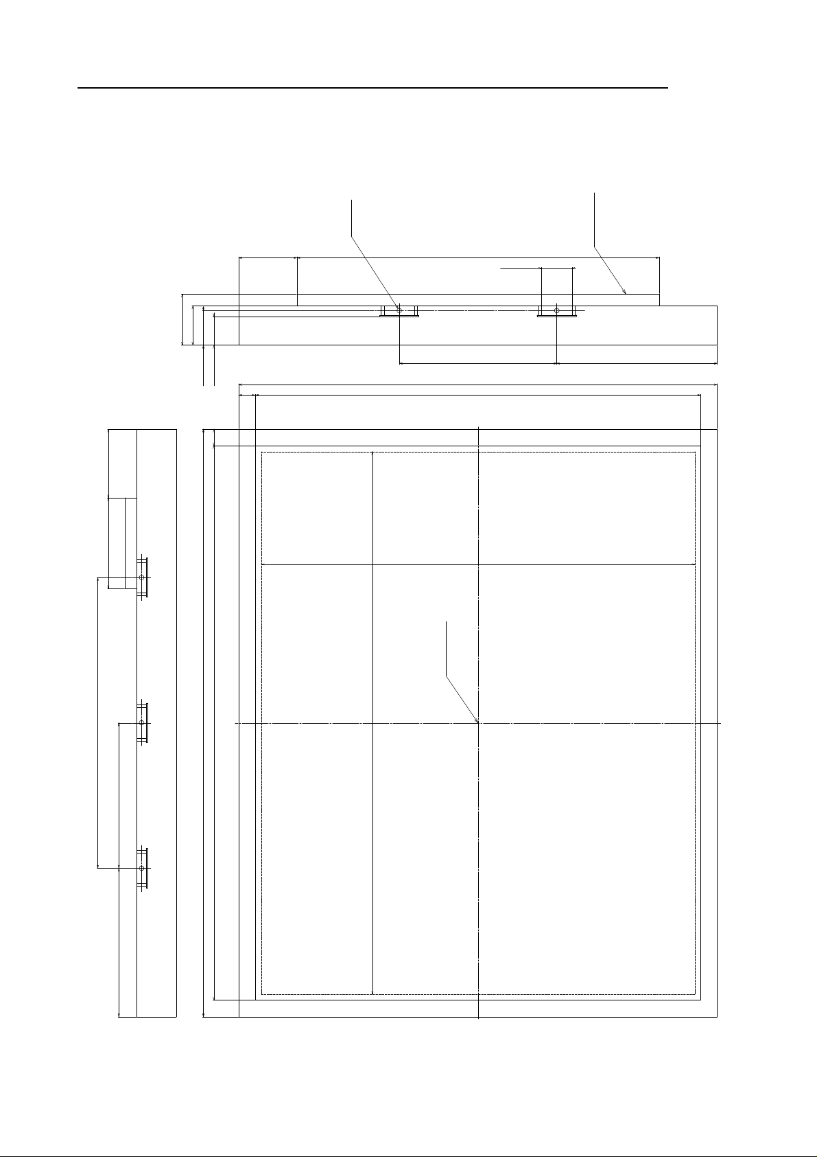
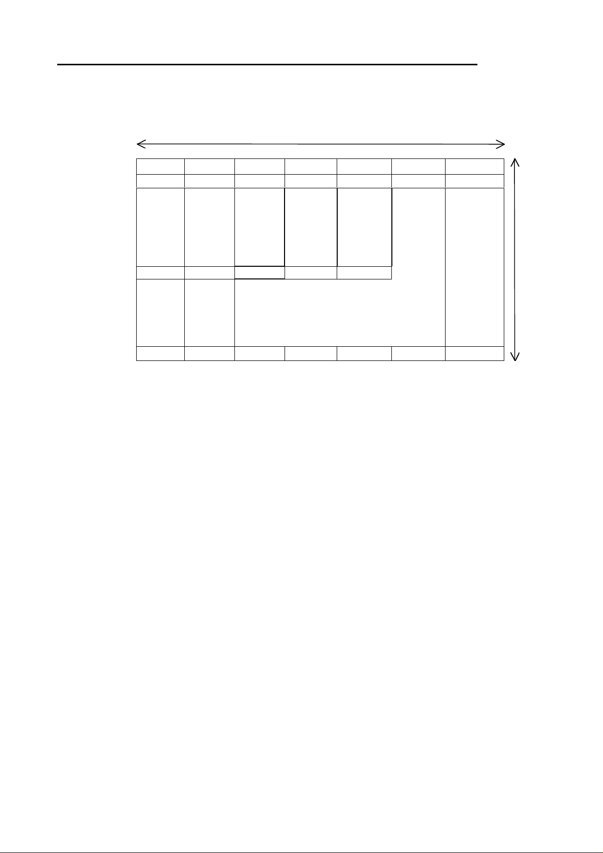
DIMENSIONAL OUTLINE (FRONT)
LTM18C161S
Unit : mm
Standard tolerance : 0.6
(10x) M3
38.6240
34
26
(10x) 23
60 45.5
11
(10x) 19
11
317.2
287.232 (Active Area)
(10x) 20
(2x) 104.4(2x) 106.4
295.2 (Bezel Opening)
INVERTER CARD
Active Area Center
389
(2x) 192.5
367 (Bezel Opening)
359.04 (Active Area)
(2x) 96.3
(2x) 98.3
(2/17)
1999-4-26(Ver.0.3)
Page 3
LTM18C161S
DIMENSINAL OUTLINE (REAR)
FRONT SURFACE OF BEZEL
2.4
Unit : mm
Standard tolerance : 0.6
SECTION A-A
(2x) 224
(10x) 1
A
(3x) 138
(8x) 6.5
(8x) M2.5
(3x) 37.5
(8x) 6.5
(2x) 28.3
A
86.7 13.3
114
156.7
(2x) 228
(3/17)
1999-4-26(Ver.0.3)
Page 4
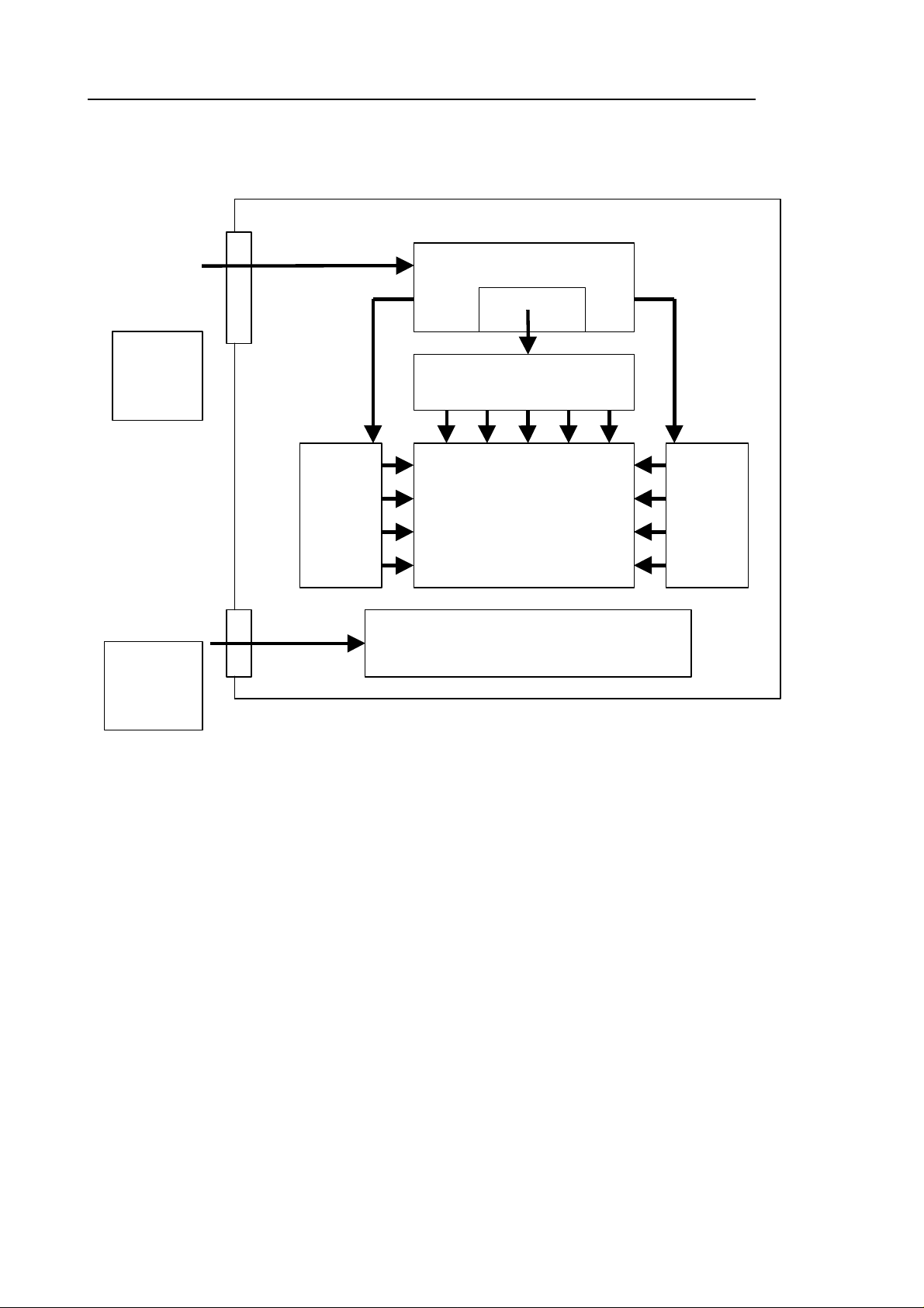
LTM18C161S
BLOCK DIAGRAM
LCD Module
Interface Signal
Connector
(30pin)
Interface card
Gatearray
+12V
LVDS
X-card
VcontIN
Backlight Signal
Connector (8pin)
+12V
VDIM
BLON
Y- card
-L
TFT/LCD
Array/Cell
1280•~1024
Backlight unit
Inverter card
Y- card
-R
(4/17)
1999-4-26(Ver.0.3)
Page 5
LTM18C161S
PIXEL FORMAT
1280 Pixels
EVEN ODD EVEN ODD ODD
0,0 1,0
x
2n
,0 x
2n-1
, 0
1279, 0
Display 0,y x
0, 1023
,y x
2n
2n-1
, y
1024 Lines
1279, 1023
(5/17)
1999-4-26(Ver.0.3)
Page 6
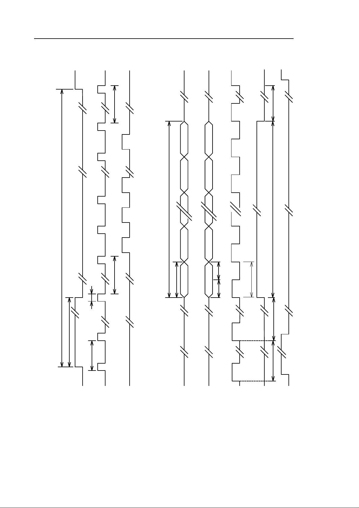
VI
VI
LTM18C161S
TIMING CHART
Thf
m
Thd
Tv
1 2 3
Tvb Tvf
Tha
0 2 n-4 n-2
Tck
n-1n-3
Thd
31
Tdh
Tck
Tds
Thb
Tva
Th
Tha
(1) Vsync, Hsync and Display Ti mi ng
Vsync
1999-4-26(Ver.0.3)
Hsync
DSPTMG
(2) Vi deo si gnal and Dot clock
DEO(EVEN)
(6/17)
DEO(ODD)
DOTCLK
DSPTMG
Hsync
Page 7

LTM18C161S
TIMING SPECIFICATION
Item Symbol Min. Typ. Max. unit Remarks
Clock Frequency Fdck 50 54 56.8 MHz
Clock Period Tck 17.6 18.5 20 ns
Frame Rate 1/Tv 56.25 60.02 61.0 Hz
Frame Period Tv 16.39 16.66 17.78 ms
V-Sync
Active Level
V-Back Porch Tvb Tv x 7 Tv x 38 Tv x 63 ms
V-Front Porch Tvf Tv x 1 --- ms
V-Line m --- Tv x 1024 --- Ms
Scan Rate 1/Th --- 63.98 --- kHz
H-Sync
Active Level
H-Back Porch Thb(*1) Tck x 4 Tck x 124 --- ns
H-Front Porch Thf Tck x 4 Tck x 24 --- ns
Display Pixels n --- Tck x 640 --- ns
Note: The typical values conform to VESA STANDARD.
(*1) : Tha+Thb should be less than 1024 Tc.
Tva Tv x 3 Tv x 3 --- ms
Tha(*1) Tck x 4 Tck x 56 --- ns
(7/17)
1999-4-26(Ver.0.3)
Page 8

LTM18C161S
CONNECTOR PIN ASSIGNMENT FOR INTERFACE
INPUT SIGNAL
The module uses a pair of LVDS receiver SN75LVDS82(Texas Instruments) or compatible. LVDS is a differential
signal technology for LCD interface and high speed data transfer device. Transfer shall be SN75LVDS83 (negative
edge sampling) or compatible.
Connector : FI-SE30P-HF or FI-S30P-HF / JAE.
Mating Connector :FI-S30S / JAE.
Terminal No. Symbol Function
1 VDD Power Supply : +12.0V
2 VDD Power Supply : +12.0V
3 VDD Power Supply : +12.0V
4 GND Gnd for VDD line
5 GND Gnd for VDD line
6 GND Gnd for VDD line
7 SELLVDS Select LVDS data order. See the following figure.
8 VcontIN Contrast signal voltage input(0-3V). Need to input stable
voltage.(*1)
9 DGND Digital Ground for VcontIN
10 RxOIN3+ Positive Transmission Clock (Odd data )
11 RxOIN3- Negative Transmission Clock (Odd data )
12 RxOCK+ Positive Transmission Data (Odd Clock)
13 RxOCK- Negative Transmission Data (Odd Clock)
14 RxOIN2+ Positive Transmission Data (Odd data )
15 RxOIN2- Negative Transmission Data (Odd data)
16 RxOIN1+ Positive Transmission Data (Odd data )
17 RxOIN1- Negative Transmission Data (Odd data)
18 RxOIN0+ Positive Transmission Data (Odd data )
19 RxOIN0- Negative Transmission Data (Odd data)
20 RXEIN3+ Positive Transmission Clock (Even data )
21 RxEIN3- Negative Transmission Clock (Even data)
22 RxECK+ Positive Transmission Data (Even Clock)
23 RxECK- Negative Transmission Data (Even Clock)
24 RxEIN2+ Positive Transmission Data (Even data)
25 RxEIN2- Negative Transmission Data (Even data)
26 RxEIN1+ Positive Transmission Data (Even data)
27 RxEIN1- Negative Transmission Data (Even data)
28 RxEIN0+ Positive Transmission Data (Even data)
29 RxEIN0- Negative Transmission Data (Even data)
30 LVDSGND Ground for LVDS Clock/Data signals
Note : Input signals of odd and even clock shall be the same timing.
(*1) 1.5V is the center of the design point.
The Gamma curve of the gray level(Level1 to Level254) will be bent towards,
0V : White side ,3V : Black side
The maximum white(Level255) and black (Level0) luminance will not change.
(8/17)
1999-4-26(Ver.0.3)
Page 9

LTM18C161S
Backlight Signal Connector
Connector : S8B-PH-SM3 / JST.
Mating Connector : PHR-8 / JST.
Terminal No. Symbol Function
1 VBL +12V Power Supply for backlight
2 VBL +12V Power Supply for backlight
3 VBL +12V Power Supply for backlight
4 GND Ground for VBL line, VDIM and BLON
5 GND Ground for VBL line, VDIM and BLON
6 GND Ground for VBL line, VDIM and BLON
7 VDIM Backlight Control Voltage Input(0-4V)
0V:Brightness MAX, 4V:Brightness MIN
8 BLON Backlight on/off signal (H : Backlight ON, L : Backlight OFF) TTL Level
(9/17)
1999-4-26(Ver.0.3)
Page 10

LTM18C161S
SELLVDS=Low or Open
RxECLKIN+
RxECLKIN-
RxEIN0+
RxEIN0-
RxEIN1+
RxEIN1-
RxEIN2+
RxEIN2-
RxEIN3+
RxEIN3-
RxOCLKI N+
RxOCLKI N-
RxOIN0+
RxOIN0-
RxOIN1+
RxOIN1-
RxOIN2+
RxOIN2-
RxOIN3+
RxOIN3-
Not e : R/ G/ B Dat a7: MSB , R/ G/ B Dat a0:LSB
ER1 ER0 EG0 ER5 ER4 ER3 ER2 ER1 ER0 EG0
EG2 EG1
EB3 EB2
ER7 ER6 NA EB7 EB6 EG7 EG6 ER7 ER6 NA
OR1 OR0 OG0 OR5
OG2 OG1 OB1 OB0
OB3 OB2 NA NA
OR7 OR6 NA
EB1 EB0 EG5 EG4
SELLVDS=Hi gh
OB7
1 cycle
EB5H- SV- SDSP
1 cycle
OR4 OR3 OR2 OR1
OG5 OG4 OG3 OG2
NA OB5 OB4 OB3
OB6 OG7 OG6 OR7
EB1EG1EG2EG3
DSPEB2EB3EB4
OR0 OG0
OG1 OB1
OB2
OR6 NA
NA
RxECLKIN+
RxECLKIN-
RxEIN0+
RxEIN0-
RxEIN1+
RxEIN1-
RxEIN2+
RxEIN2-
RxEIN3+
RxEIN3-
RxOCLKI N+
RxOCLKI N-
RxOIN0+
RxOIN0-
RxOIN1+
RxOIN1-
RxOIN2+
RxOIN2-
RxOIN3+
RxOIN3-
Not e : R/ G/ B Dat a7: MSB , R/ G/ B Dat a0:LSB
ER3 ER2 EG2
EG4 EG3 EB3
EB5 EB4
ER0ER1
OR3 OR2 OG2 OR7
OB5 OB4
OR1 OR0
NA NA
OB3
NA NA
NA
1 cycle
ER7 ER6 ER5 ER4 ER3
EG4EG5EG6EG7EB2
EB7 EB6 EB5
ER1EG0EG1EB0EB1
1 cycle
OR6
OG7OB2OG4 OG3
NA
OB0OB1
OR5
OG6
OB7
OG5
OB6
OG0OG1
OR3OR4
OG4
OB5
ER2 EG2
EG3
EB4
ER0
OG3
OB4
OR0OR1
EB3
DSPH-SV-SDSP
OG2OR2
OB3
NA
NA
(10/17)
1999-4-26(Ver.0.3)
Page 11

LTM18C161S
Recommended Transmitter (SN75LVDS83DGG) to LTM18C161S Interface Assignment
SELLVDS = Low or Open
T1(Odd Pixels Data) Signal Interface : Transmitter(SN75LVDS83DGG)
Input Terminal Input Signal(Graphics controller output signal)
Number Symbol Symbol Function
51 T1IN0 RO0 RED Odd pixels DISPLAY DATA (LSB)
52 T1IN1 RO1 RED Odd pixels DISPLAY DATA
54 T1IN2 RO2 RED Odd pixels DISPLAY DATA
55 T1IN3 RO3 RED Odd pixels DISPLAY DATA
56 T1IN4 RO4 RED Odd pixels DISPLAY DATA
3 T1IN6 RO5 RED Odd pixels DISPLAY DATA
4 T1IN7 GO0 GREEN Odd pixels DISPLAY DATA (LSB)
6 T1IN8 GO1 GREEN Odd pixels DISPLAY DATA
7 T1IN9 GO2 GREEN Odd pixels DISPLAY DATA
11 T1IN12 GO3 GREEN Odd pixels DISPLAY DATA
12 T1IN13 GO4 GREEN Odd pixels DISPLAY DATA
14 T1IN14 GO5 GREEN Odd pixels DISPLAY DATA
15 T1IN15 BO0 BLUE Odd pixels DISPLAY DATA (LSB)
19 T1IN18 BO1 BLUE Odd pixels DISPLAY DATA
20 T1IN19 BO2 BLUE Odd pixels DISPLAY DATA
22 T1IN20 BO3 BLUE Odd pixels DISPLAY DATA
23 T1IN21 BO4 BLUE Odd pixels DISPLAY DATA
24 T1IN22 BO5 BLUE Odd pixels DISPLAY DATA
27 T1IN24 NA
28 T1IN25 NA
30 T1IN26 NA
50 T1IN27 RO6 RED Odd pixels DISPLAY DATA
2 T1IN5 RO7 RED Odd pixels DISPLAY DATA (MSB)
8 T1IN10 GO6 GREEN Odd pixels DISPLAY DATA
10 T1IN11 GO7 GREEN Odd pixels DISPLAY DATA (MSB)
16 T1IN16 BO6 BLUE Odd pixels DISPLAY DATA
18 T1IN17 BO7 BLUE Odd pixels DISPLAY DATA (MSB)
25 T1IN23 NA
31 T1CLK IN NCLK DATA SAMPLING CLOCK T1CLK OUT-
Output Signal
Symbol
T1OUT0T1OUT0+
T1OUT1T1OUT1+
T1OUT2T1OUT2+
T1OUT3T1OUT3+
T1CLK OUT+
To LTM18C161
Interface
Terminal:Symbol
No.18
No.19
No.16
No.17
No.14
No.15
No.10
No.11
No.12
No.13
(11/17)
1999-4-26(Ver.0.3)
Page 12

T2(Even Pixels Data) Signal Interface : Transmitter(SN75LVDS83DGG)
Input Terminal Input Signal(Graphics controller output signal)
Number Symbol Symbol Function
51 T2IN0 RE0 RED Even pixels DISPLAY DATA (LSB)
52 T2IN1 RE1 RED Even pixels DISPLAY DATA
54 T2IN2 RE2 RED Even pixels DISPLAY DATA
55 T2IN3 RE3 RED Even pixels DISPLAY DATA
56 T2IN4 RE4 RED Even pixels DISPLAY DATA
3 T2IN6 RE5 RED Even pixels DISPLAY DATA
4 T2IN7 GE0 GREEN Even pixels DISPLAY DATA (LSB)
6 T2IN8 GE1 GREEN Even pixels DISPLAY DATA
7 T2IN9 GE2 GREEN Even pixels DISPLAY DATA
11 T2IN12 GE3 GREEN Even pixels DISPLAY DATA
12 T2IN13 GE4 GREEN Even pixels DISPLAY DATA
14 T2IN14 GE5 GREEN Even pixels DISPLAY DATA
15 T2IN15 BE0 BLUE Even pixels DISPLAY DATA (LSB)
19 T2IN18 BE1 BLUE Even pixels DISPLAY DATA
20 T2IN19 BE2 BLUE Even pixels DISPLAY DATA
22 T2IN20 BE3 BLUE Even pixels DISPLAY DATA
23 T2IN21 BE4 BLUE Even pixels DISPLAY DATA
24 T2IN22 BE5 BLUE Even pixels DISPLAY DATA
27 T2IN24 H-S H-sync
28 T2IN25 V-S V-sync
30 T2IN26 DSP DISPLAY TIMING
50 T2IN27 RE6 RED Even pixels DISPLAY DATA
2 T2IN5 RE7 RED Even pixels DISPLAY DATA (MSB)
8 T2IN10 GE6 GREEN Even pixels DISPLAY DATA
10 T2IN11 GE7 GREEN Even pixels DISPLAY DATA (MSB)
16 T2IN16 BE6 BLUE Even pixels DISPLAY DATA
18 T2IN17 BE7 BLUE Even pixels DISPLAY DATA (MSB)
25 T2IN23 NA
31 T2CLK IN NCLK DATA SAMPLING CLOCK T2CLK OUT-
Output Signal
Symbol
T2OUT0T2OUT0+
T2OUT1T2OUT1+
T2OUT2T2OUT2+
T2OUT3T2OUT3+
T2CLK OUT+
LTM18C161S
To LTM18C161
Interface
Terminal:Symbol
No.28
No.29
No.26
No.27
No.24
No.25
No.20
No.21
No.22
No.23
(12/17)
1999-4-26(Ver.0.3)
Page 13

LTM18C161S
SELLVDS=High
T1(Odd Pixels Data) Signal Interface : Transmitter(SN75LVDS83DGG)
Input Terminal Input Signal(Graphics controller output signal)
Number Symbol Symbol Function
51 T1IN0 RO2 RED Odd pixels DISPLAY DATA
52 T1IN1 RO3 RED Odd pixels DISPLAY DATA
54 T1IN2 RO4 RED Odd pixels DISPLAY DATA
55 T1IN3 RO5 RED Odd pixels DISPLAY DATA
56 T1IN4 RO6 RED Odd pixels DISPLAY DATA
3 T1IN6 RO7 RED Odd pixels DISPLAY DATA (MSB)
4 T1IN7 GO2 GREEN Odd pixels DISPLAY DATA
6 T1IN8 GO3 GREEN Odd pixels DISPLAY DATA
7 T1IN9 GO4 GREEN Odd pixels DISPLAY DATA
11 T1IN12 GO5 GREEN Odd pixels DISPLAY DATA
12 T1IN13 GO6 GREEN Odd pixels DISPLAY DATA
14 T1IN14 GO7 GREEN Odd pixels DISPLAY DATA (MSB)
15 T1IN15 BO2 BLUE Odd pixels DISPLAY DATA
19 T1IN18 BO3 BLUE Odd pixels DISPLAY DATA
20 T1IN19 BO4 BLUE Odd pixels DISPLAY DATA
22 T1IN20 BO5 BLUE Odd pixels DISPLAY DATA
23 T1IN21 BO6 BLUE Odd pixels DISPLAY DATA
24 T1IN22 BO7 BLUE Odd pixels DISPLAY DATA (MSB)
27 T1IN24 NA
28 T1IN25 NA
30 T1IN26 NA
50 T1IN27 RO0 RED Odd pixels DISPLAY DATA (LSB)
2 T1IN5 RO1 RED Odd pixels DISPLAY DATA
8 T1IN10 GO0 GREEN Odd pixels DISPLAY DATA (LSB)
10 T1IN11 GO1 GREEN Odd pixels DISPLAY DATA
16 T1IN16 BO0 BLUE Odd pixels DISPLAY DATA (LSB)
18 T1IN17 BO1 BLUE Odd pixels DISPLAY DATA
25 T1IN23 NA
31 T1CLK IN NCLK DATA SAMPLING CLOCK T1CLK OUT-
Output Signal
Symbol
T1OUT0T1OUT0+
T1OUT1T1OUT1+
T1OUT2T1OUT2+
T1OUT3T1OUT3+
T1CLK OUT+
To LTM18C161
Interface
Terminal:Symbol
No.18
No.19
No.16
No.17
No.14
No.15
No.10
No.11
No.12
No.13
(13/17)
1999-4-26(Ver.0.3)
Page 14

LTM18C161S
T2(Even Pixels Data) Signal Interface : Transmitter(SN75LVDS83DGG)
Input Terminal Input Signal(Graphics controller output signal)
Number Symbol Symbol Function
51 T2IN0 RE2 RED Even pixels DISPLAY DATA
52 T2IN1 RE3 RED Even pixels DISPLAY DATA
54 T2IN2 RE4 RED Even pixels DISPLAY DATA
55 T2IN3 RE5 RED Even pixels DISPLAY DATA
56 T2IN4 RE6 RED Even pixels DISPLAY DATA
3 T2IN6 RE7 RED Even pixels DISPLAY DATA (MSB)
4 T2IN7 GE2 GREEN Even pixels DISPLAY DATA
6 T2IN8 GE3 GREEN Even pixels DISPLAY DATA
7 T2IN9 GE4 GREEN Even pixels DISPLAY DATA
11 T2IN12 GE5 GREEN Evenpixels DISPLAY DATA
12 T2IN13 GE6 GREEN Even pixels DISPLAY DATA
14 T2IN14 GE7 GREEN Even pixels DISPLAY DATA (MSB)
15 T2IN15 BE2 BLUE Even pixels DISPLAY DATA
19 T2IN18 BE3 BLUE Even pixels DISPLAY DATA
20 T2IN19 BE4 BLUE Even pixels DISPLAY DATA
22 T2IN20 BE5 BLUE Even pixels DISPLAY DATA
23 T2IN21 BE6 BLUE Even pixels DISPLAY DATA
24 T2IN22 BE7 BLUE Even pixels DISPLAY DATA (MSB)
27 T2IN24 H-S H-sync
28 T2IN25 V-S V-sync
30 T2IN26 DSP DISPLAY TIMING
50 T2IN27 RE0 RED Even pixels DISPLAY DATA (LSB)
2 T2IN5 RE1 RED Even pixels DISPLAY DATA
8 T2IN10 GE0 GREEN Even pixels DISPLAY DATA (LSB)
10 T2IN11 GE1 GREEN Even pixels DISPLAY DATA
16 T2IN16 BE0 BLUE Even pixels DISPLAY DATA (LSB)
18 T2IN17 BE1 BLUE Even pixels DISPLAY DATA
25 T2IN23 NA
31 T2CLK IN NCLK DATA SAMPLING CLOCK T2CLK OUT-
Output Signal
Symbol
T2OUT0T2OUT0+
T2OUT1T2OUT1+
T2OUT2T2OUT2+
T2OUT3T2OUT3+
T2CLK OUT+
To LTM18C161S
Interface
Terminal:Symbol
No.28
No.29
No.26
No.27
No.24
No.25
No.20
No.21
No.22
No.23
The following is LVDS Signal description.
LVDS Data Name Description
DSP Display
Timing
V-S Vertical Sync Both Positive and negative polarities are acceptable.
H-S Horizontal
Sync
Note: Output signals from any system shall be low or Hi-Z state when VDD is off.
When the signal is high, the pixel data shall be valid to be displayed.
Both Positive and negative polarities are acceptable.
(14/17)
1999-4-26(Ver.0.3)
Page 15

LTM18C161S
Interface Signal Electrical Characteristics
Input signal shall be low or Hi-Z state when VDD is off.
It is recommended to refer the specifications of SN75LVDS82DGG (Texas Instruments) in detail.
Signal electrical characteristics are as follows.
Symbol Condition Min. Max unit
Vth Differential Input High Voltage
100 mV
(Vcom=+1.2V)
Vtl Differential Input High Voltage
-100 mV
(Vcom=+1.2V)
7x CLK
(internal )
SETUP
LVDS Data
HOLD
Name Description Min. Typ. Max. unit
SETUP Time 800 - - psLVDS Data
HOLD Time 800 - - ps
Name Description Min. Typ. Max. unit Note
SELLVDS
High Voltage 2 3 3.3 V
Low Voltage -0.1 0 0.7 V
Current -1 - mA
VcontIN
Input Voltage range 0 3 V 0V : towards white side
3V : towards black side
Current -1 1 mA
(15/17)
1999-4-26(Ver.0.3)
Page 16

LTM18C161S
256k (k=1024) COLORS COMBINATION TABLE
Basic
Color
Gray
Scale
of Red
Gray
Scale
of
Green
Gray
Scale
of
Blue
Gray
Scale
of
White
&
Black
Display
Black
Blue
Green
Light Blue
Red
Purple
Yellow
White
Black
Dark
↑
↓
Light
Red
Black
Dark
↑
↓
Light
Green
Black
Dark
↑
↓
Light
Blue
Black
Dark
↑
↓
Light
White
R7 R6 R5 R4 R3 R2 R1 R0
LLLLLLLL LLLLLLLL LLLLLLLL LLLLLLLL LLLLLLLL HHHHHHHH LLLLLLLL HHHHHHHH LLLLLLLL LLLLLLLL HHHHHHHH HHHHHHHH HHHHHHHH LLLLLLLL LLLLLLLL HHHHHHHH LLLLLLLL HHHHHHHH HHHHHHHH HHHHHHHH LLLLLLLL HHHHHHHH HHHHHHHH HHHHHHHH LLLLLLLL LLLLLLLL LLLLLLLL L 0
LLLLLLLH LLLLLLLL LLLLLLLL L 1
LLLLLLHL LLLLLLLL LLLLLLLL L 2
LLLLLLHH LLLLLLLL LLLLLLLL L 3
LLLLLHLL LLLLLLLL LLLLLLLL L 4
:
:
HHHHHHLH LLLLLLLL LLLLLLLL L253
HHHHHHHL LLLLLLLL LLLLLLLL L254
HHHHHHHH LLLLLLLL LLLLLLLL Red L255
LLLLLLLL LLLLLLLL LLLLLLLL L 0
LLLLLLLL LLLLLLLH LLLLLLLL L 1
LLLLLLLL LLLLLLHL LLLLLLLL L 2
LLLLLLLL LLLLLLHH LLLLLLLL L 3
LLLLLLLL LLLLLHLL LLLLLLLL L 4
:
:
LLLLLLLL HHHHHHLH LLLLLLLL L253
LLLLLLLL HHHHHHHL LLLLLLLL L254
LLLLLLLL HHHHHHHH LLLLLLLL Green L255
LLLLLLLL LLLLLLLL LLLLLLLL L 0
LLLLLLLL LLLLLLLL LLLLLLLH L 1
LLLLLLLL LLLLLLLL LLLLLLHL L 2
LLLLLLLL LLLLLLLL LLLLLLHH L 3
LLLLLLLL LLLLLLLL LLLLLHLL L 4
:
:
LLLLLLLL LLLLLLLL HHHHHHLH L243
LLLLLLLL LLLLLLLL HHHHHHHL L254
LLLLLLLL LLLLLLLL HHHHHHHH Blue L255
LLLLLLLL LLLLLLLL LLLLLLLL L 0
LLLLLLLH LLLLLLLH LLLLLLLH L 1
LLLLLLHL LLLLLLHL LLLLLLHL L 2
LLLLLLHH LLLLLLHH LLLLLLHH L 3
LLLLLHLL LLLLLHLL LLLLLHLL L 4
:
:
HHHHHHLH HHHHHHLH HHHHHHLH L253
HHHHHHHL HHHHHHHL HHHHHHHL L254
HHHHHHHH HHHHHHHH HHHHHHHH White L255
G7 G6 G5 G4 G3 G2 G1 G0
:
:
:
:
:
:
:
:
B7 B6 B5 B4 B3 B2 B1 B0
:
:
:
:
:
:
:
:
Gray Scale
Level
L5…
L252
L5…
L252
L5…
L252
L5…
L252
(16/17)
1999-4-26(Ver.0.3)
Page 17

!
LTM18C161S
FOR SAFETY
LCD module is generally designed with precise parts to achieve light weighted thin mechanical dimensions.
In using our Modules, make certain that you fully understand and put into practice the warnings and safety precautions
detailed in Engineering Information No.EE-N001,"CAUTIONS AND INSTRUCTIONS FOR TOSHIBA LCD MODULES".
Refer to individual specifications and TECHNICAL DATA sheets (hereinafter called "TD") for more detailed technical
information.
1) SPECIAL PURPOSES
A) Toshiba's Standard LCD Modules have not been customized for operation in extreme environments or for use in
applications where performance failures could be life-threatening or otherwise catastrophic.
B) Since Toshiba's Standard LCD Modules have not been designed for operation in extreme environments, they must never
be used in devices that will be exposed to abnormally high levels of vibration or shock which exceed Toshiba's published
specification limits.
C) In addition, since Toshiba Standard LCD Modules have not been designed for use in applications where performance
failures could be life-threatening or catastrophic, they must never be installed in aircraft navigation control systems (such as,
but not limited to Traffic Collision Avoidance System and Air Traffic Indicator), in military defense or weapons systems, in
critical industrial process-control systems (e.g., those involved in the production of nuclear energy), or in critical medical
device or patient life-support systems.
2) DISASSEMBLING OR MODIFICATION
DO NOT DISASSEMBLE OR MODIFY the module. It may damage sensitive parts inside LCD module, and may cause
scratches or dust on the display.
Toshiba doses not warrant the module, if customer disassembled or modified it.
3) BREAKAGE OF LCD PANEL
DO NOT INGEST liquid crystal material, DO NOT INHALE this material, and DO NOT CONTACT the material with skin, if
LCD panel is broken and liquid crystal material spills out.
If liquid crystal material comes into mouth or eyes, rinse mouth or eyes out with water immediately.
If this material contact with skin or cloths, wash it off immediately with alcohol and rinse thoroughly with water.
4) GLASS OF LCD PANEL
BE CAREFUL WITH CHIPS OF GLASS that may cause injuring fingers or skin, when the glass is broken.
5) ELECTRIC SHOCK
DISCONNECT POWER SUPPLY before handling LCD module.
DO NOT TOUCH the parts inside LCD module and the fluorescent lamp's connector or cables in order to prevent electric
shock, because high voltage is supplied to these parts from the inverter unit while power supply is turned on.
6) ABSOLUTE MAXIMUM RATINGS AND POWER PROTECTION CIRCUIT
DO NOT EXCEED the absolute maximum rating values under the worst probable conditions caused by the supply voltage
variation, input voltage variation, variation in parts' constants, environmental temperature, etc., otherwise LCD module may
be damaged.
Employ protection circuit for power supply, whenever the specification or TD specifies it.
Suitable protection circuit should be applied for each system design.
7)
DISPOSAL
When dispose LCD module, obey to the applicable environmental regulations.
(17/17)
1999-4-26(Ver.0.3)
 Loading...