

Page 1
LTD154EZ1D Sheet 1
1. Product Specifications
1.1 General Specifications
Item Specifications
Display Mode TN color(64 gray scales, 262,144 colors)
Transmissive type, Normally white
Viewing Direction 6 o'clock (in direction of maximum contrast)
Driving Method TFT active matrix
Input Signals LVDS interface
RxOCLK+, RxOCLK-, RxECLK+,RxECLK-
RxOIN0+, RxOIN0-, RxEIN0+, RxEIN0-,
RxOIN1+, RxOIN1-, RxEIN1+, RxEIN1-
RxOIN2+, RxOIN2-, RxEIN2+, RxEIN2Display Area
Bezel Opening
Number of Pixels
Pixel Pitch
Pixel Arrange men t RGB vertical stripes
Surface Tr eatment Anti-Reflection and hard coat 3H on LCD surface
Backlight Single cold-cathode fluorescent lamp for sidelig hting
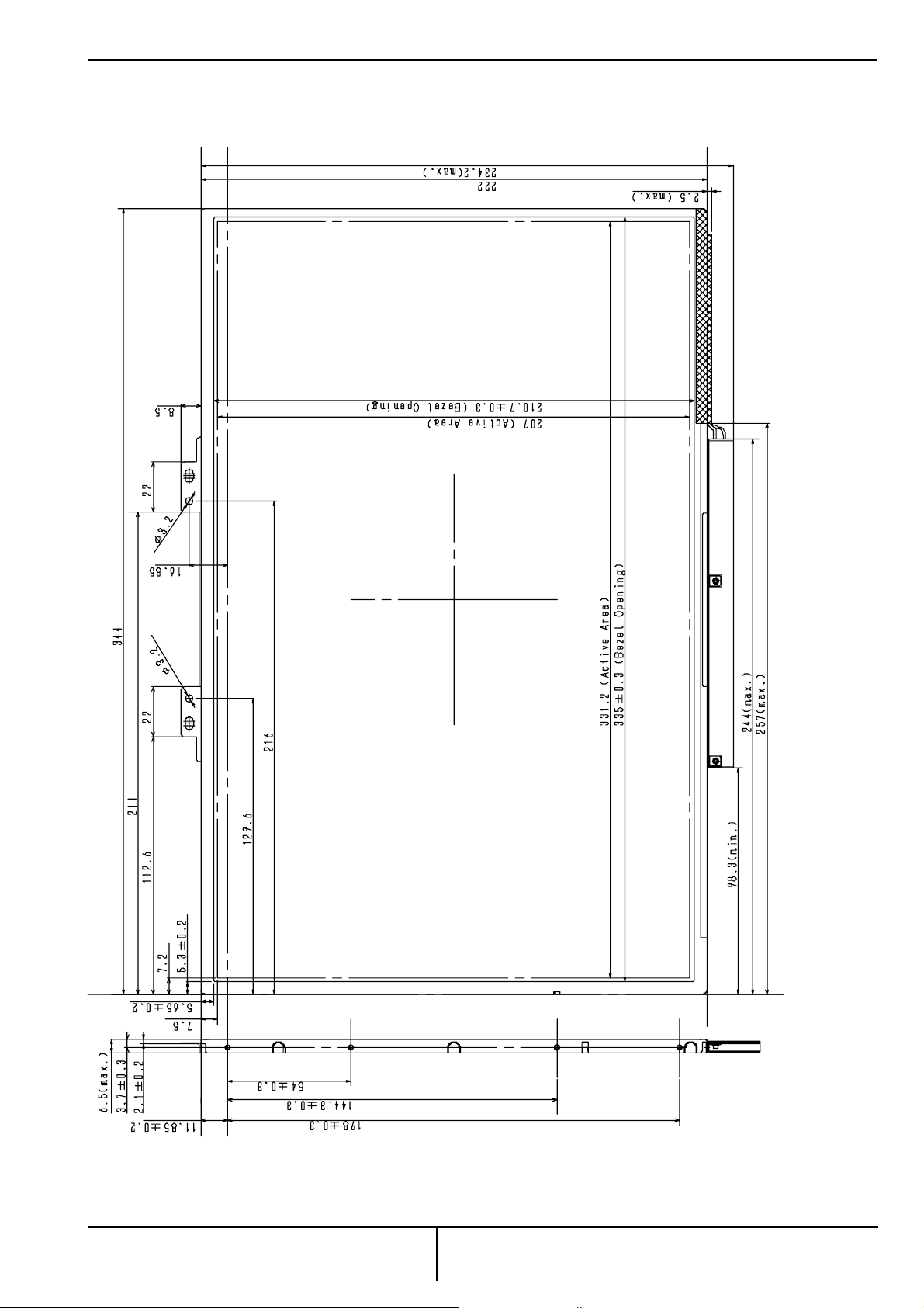
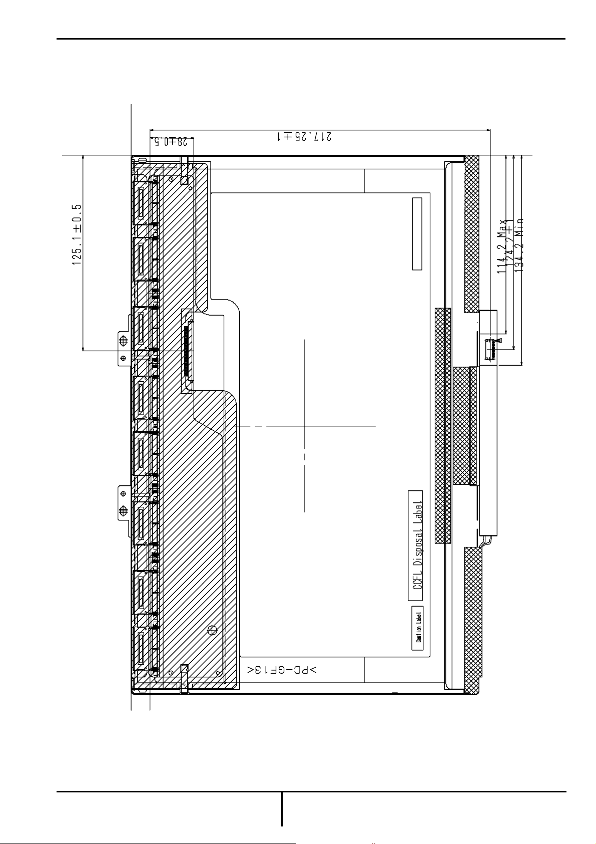
Dimensional Outline
Inverter SMBus Controlled for Brightness
EDID SPWG Version 2.0, (2001-9-4)
E2ROM Data Address A0h
Note 1)
1 2 1919 1920
R G B
R G B
1
2
R G B
R G B
R G B
R G B
1199
R G B
R G B
1200
331.2 (W ) × 207.0 (H ) (mm)
335.0 (W ) × 210.7 (H ) (mm)
1920 (W ) × 1200 (H )
0.1725 (W ) × 0.1725 (H ) (mm)
344.5max. (W ) × 222.5max. (H ) × 6.5max. (D ) (mm)
1)
R G B
R G B
R G B
R G B
1)
R G B
R G B
R G B
R G B
1)
R G B
R
G
0.1725mm
: pixel
B
: Sub-pixel
(Dots)
0.1725mm
1.2 Mechanical Specifications
1.2.1 Weight
LCD Module : 600g (Max.)
* Without Inverter
Toshiba Mobile Display Co., Ltd
Date: 2009-07-30
Page 2
LTD154EZ1D Sheet 2
1.2.2 Dimensional Outline Unit : mm
(front figure) Sta ndard Tolerance: ±0.5
Toshiba Mobile Display Co., Ltd
Date: 2009-07-30
Page 3
LTD154EZ1D Sheet 3
(back figure) Standa rd Tolerance: ±0.5
Unit : mm
Toshiba Mobile Display Co., Ltd
Date: 2009-07-30
Page 4

LTD154EZ1D Sheet 4
1.3 Electrical Specifications
1.3.1 Circuit Diagram
J
E
A
FI-XB30SRL- HF11
I/F Connector
Lock Type
Interface card
Gatearray
Source Driver IC
Liquid Cristal Panel
1920 x 1200 Pixels
CN2
LVC-D20SFYG(HONDA)
Backlight
I/F Connector
Inverter
1.3. Sequence of Power Supplies and Signals
LVDSLVDS
JST
BHSMR-02VS-1
10ms(Max.)
3
.
0
V
DD
V
RxOCLK+, RxECLK+
RxOIN0+
RxEIN0+
RxOCLK-, RxECLKRxOIN0RxEIN0-
RxOIN2+
RxEIN2+
RxOIN2-
RxEIN2-
0.2V
10%
Inverter(VIN/5VALW)
Inverter(SMB CLK/SMB DATA)
Inverter(Von/off)
40ms(Max.)
M
(
s
m
0
.
n
i
100ms(Min.)
m
0
(
s
10ms(Max.)
V
0
.
3
40ms(Max.)
s
m
)
.
n
i
M
)
M
(
s
m
0
0
)
.
n
i
)
.
n
i
M
(
10%
0
(
s
m
m
0
n
i
M
(
s
.
5
0.2V
i
n
.
s
0
m
n
i
M
)
)
(
M
)
.
0.2V
)
.
n
i
M
(
s
m
0
0
Toshiba Mobile Display Co., Ltd
Date: 2009-07-30
Page 5

LTD154EZ1D Sheet 5
1.3.3 Timing Chart
(1) Vertical Timing
Tvp
VSPW VSPW
VSYNC
tvsu tvhd VA VBL
HSYNC
Tvbp Tvfp
DE
Data
CLK
(2) Horizontal Timing
HSPW ta HSPW
HSYNC
DE
ODD-Data
EVEN-Data
CLK
X,1199 X,1200X,1 X,2
Thp
Thbp Thfp
1,Y 3,Y 5,Y 1915,Y 1917,Y 1919,Y
2,Y 4,Y 6,Y 1916,Y 1918,Y 1920,Y
Tc
HA HBL
Toshiba Mobile Display Co., Ltd
Date: 2009-07-30
Page 6

LTD154EZ1D Sheet 6
1.3.4 Timing Specifications
1) 2) 3) 4) 5) 6) 7)
Item Symbol min. typ. max. unit
Thp
H-sync Pulse Width
Horizontal Front Porch thfp 4 - 136 Tc
Horizontal Back Porch
Horizontal Sync Term
Horizontal Blanking Term
Horizontal Display Term
V-sync Pulse Width
V-sync Set Up Time (to H -sync) tvsu 8 - - Tc
V-sync Hold Time tvhd 8 - - Tc
Vertical Front Porch tvfp 8 - - Tc
Vertical Back Porch
Vertical Blanking Term
Vertical Display Term
DE Pulse Width
Clock Period Tc 13.179 13.179 - ns
*8)
*8)
*8)
HSPW
Thbp
ta
HBL
HA
Tvp
VSPW
Tvbp 4 - - Tc
VBL
VA
HA
- 1024 - Tc Horizontal Scanning Term
- 13.50 - us
4 - 136 Tc
16 - - Tc
4 - -
- 64 - Tc
960 960 960 Tc
- 1235 - Thp Frame Period
- 16.67 16.67 ms
1 - - Thp
- 35 - Thp
1200 1200 1200 Thp
960 960 960 Tc
Tc
Note 1) Refer to “Timing Chart” and LVDS (DS90CF366) specifications by National Semiconductor Co., Ltd.
Note 2) If ENAB is fixed to "H" or "L" level for certain period while NCLK is suppli ed, the panel displays black with some flicker.
Note 3) If NCLK is fixed to "H" or "L" level for certain period while ENAB is supplied, the panel may be damaged.
Note 4) Please adjust LCD operating signal timing and FL driving frequency, to optimize the display quality.
There is a possibility that flicker is observed by t he interference of LCD operating signal timing and FL driving condition
(especially driving frequency), even if the condition satisfies above timing specifications and recommended operatin g
conditions shown in 3.
Note5 ) Do not make tv, tvdh and tvds fluctuate.
If tv, tvdh, and tvds are fluctuate, the panel displays black.
Note6) In case of using the long frame period, the deterioration of display quality, noise etc. may be occurred.
Note7) NCLK count of each Horizontal Scanning Time should be always the same.
V-Blanking period should be “n” X “Horizontal Scanning Time”. (n: integer)
Frame period should be always the same.
Note 8) Please keep below equations.
VBL = Tvfp + Tvbp
HSPW = HBL – Thfp – ta
Thbp = HSPW + ta
Toshiba Mobile Display Co., Ltd
Date: 2009-07-30
Page 7

LTD154EZ1D Sheet 7
1.3.5 Interface Connector
1)
CN1 INPUT SIGNAL (FI-XB30SRL-HF11 / JAE)
[ Mating Connector :Wire Type FI-X30H(Housing), FI-XC3-1-15000(Contact)
FPC Type FI-X30M or FI-X30MR, Coax Type FI-X30C or FI-X30C2(Housing), FI-X30CH-7000(Sh el l)]
Terminal No. Symbol Function
1 V
2 V
3 V
4 V
SS
DD
DD
EDID
5 TEST Panel BIST Enable
6 CLK
7 DATA
EDID
EDID
8 RxOIN0- Negative LVDS differential data input (Odd), [R0-R5, G0]
9 RxOIN0+ Positive LVDS differential data input (Odd), [R0-R5, G0]
10 V
SS
11 RxOIN1- Negative LVDS differential data input (Odd), [G1-G5, B0-B1]
12 RxOIN1+ Positive LVDS differential data input (Odd), [G1-G5, B0-B1]
13 V
SS
14 RxOIN2- Negative LVDS differen t ia l da ta input (Odd), [B2-B5, HS, VS , DE]
15 RxOIN2+ Positive LVDS differential data input (Odd), [B2-B5, HS, VS, DE]
16 V
SS
17 RxOCLKIN- Negative LVDS differential clock input (Odd)
18 RxOCLKIN+ Positive LVDS differential clock input (Odd)
19 V
SS
20 RxEIN0- Negative LVDS differential data input (Even), [R0-R5, G0]
21 RxEIN0+ Positive LVDS differential data input (Even), [R0-R5, G0]
22 V
SS
23 RxEIN1- Negative LVDS different ia l da ta input (Even), [G1-G5, B0 -B1 ]
24 RxEIN1+ Positive LVDS dif ferential data input (Even), [G1-G5, B0-B1]
25 V
SS
26 RxEIN2- Negative LVDS different ia l da ta input (Even), [B2-B 5, HS, V S , D E]
27 RxEIN2+ Positive LVDS differential data input (Even), [B2-B5, HS, VS, DE]
28 V
SS
29 RxECLKIN- Negative LVDS differential clock input (Even)
30 RxECLKIN+ Positive LVDS differential clock input (Even)
GND
POWER SUPPLY : +3.3V
POWER SUPPLY : +3.3V
DDC 3.3V POWER SUPPLY : +3.3V
DDC Clock
DDC Data
GND
GND
GND
GND
GND
GND
GND
CN2 INVERTER INPUT SIGNAL (LVC-D20SFYG / HONDA)
Terminal No. Symbol Functio n
1 V
2
3
IN
V
IN
V
IN
4 NC Non connection
5 GND GND
6 NC Non connection
7 5VALW Power Source for SMBus : 4.85V~5.2V
8 GND GND
9 SMB_DA TA SMBus interface for sending brightne ss inf or m at io n (Da ta pin)
10 SMB_CLK SMBus interface for sending brigh t ne ss inf or m at io n (C lo ck p in)
11 GND GND
12 V
ON/OFF
13 GND GND
14 LAMP_STATUS FL status, ON/OFF
15 NC Non connection
16 NC Non connection
17 NC Non connection
18 NC Non connection
19 NC Non connection
20 NC Non connection
Supply Voltage : 9V~21V
Supply Voltage : 9V~21V
Supply Voltage : 9V~21V
Backlight ON/OFF control signal (1-ON, 0-OFF)
Note 1) Please connect NC pin to nothing. Don’t connect it to grand nor to other signal input.
Please connect GND to ground. Don’t use it as no-connect nor connection with high impedance.
Note 2) 262,144 colors are displayed by the combinations of 18 bits data.
Toshiba Mobile Display Co., Ltd
Date: 2009-07-30
 Loading...