

Page 1
Global LCD Panel Exchange Center
www.panelook.com
One step solution for LCD / PDP / OLED panel application: Datasheet, inventory and accessory!
www.panelook.com
Page 2
Global LCD Panel Exchange Center
Specification No.
Revision History
Date Rev Sheet
(New)
www.panelook.com
G050032-C971
Item Old New Reason
Sheet 1
Toshiba Matsushita Display Technology Co.,Ltd
Date:2004-11-04 New No.NR-LTD121EC5V-11
Date: - - Old No.
m# Special m Addition m Change
One step solution for LCD / PDP / OLED panel application: Datasheet, inventory and accessory!
www.panelook.com
Page 3
Global LCD Panel Exchange Center
Specification No.
Caution and Handling Precaution
For your end user's safety, it is strongly advised that the items with"¼"should be included in the instruction manual of the
system which may be issued by your organization.
For Safety
www.panelook.com
G050032-C971
Sheet 2
(1) Toshiba Matsushita Display Technology's Standard LCD modules have not been customized for operation in extreme
(2) DISCONNECT POWER SUPPLY before handling LCD module.
(3) Make sure to insert the module FL connector to the inverter connector in correct position.
Do not insert in irregular position.
If incorrect, this may cause smoke or burn of electrical parts by high voltage of FL circuit.
DO NOT USE the mating FL connector which Toshiba Matsushita Display Technology does not specify.
Warning
environments or for use in applications where performance failures could be life-threatening or otherwise catastrophic.
Since they must never be installed in aircraft navigation control systems (such as, but not limited to Traffic Collision
System and Air traffic Indicator), in military defense or weapons systems, in critical industrial process-control systems
(e.g., those involved in the production of nuclear energy), or in critical medical device or patient life-support systems.
DO NOT TOUCH the parts inside LCD module and the fluorescent lamp's (hereinafter called "FL") connector or cable in
order to prevent electric shock, because high voltage is supplied to these parts from the inverter unit while power supply
is turned on.
If there is a possibility that the connector has been inserted incorrectly, please re-insert the connector only after you
confirm the module and FL power is completely off. When disconnecting connector, do not pull on the cable.
Otherwise, Toshiba Matsushita Display Technology shall not be liable for any damages caused by the connector.
(1) DO NOT DISASSEMBLE OR MODIFY the module.
¼(2) DO NOT INGEST liquid crystal material, DO NOT INHALE this material, and DO NOT PERMIT this material to contact
¼(3) BE CAREFUL WITH CHIPS OF GLASS that may cause injuring fingers or skin, when the glass is broken.
Since FL is also made of glass, when FL is built in, handle it with due caution a well.
(4) Be careful with handling the metal flame (bezel) of a module. Even though burr disposal treatment is performed, it may
(5) DO NOT EXCEED the absolute maximum rating values under the worst probable conditions caused by the supply
Caution
Sensitive parts inside LCD module may be damaged, and dusts or scratches may mar the displays.
Toshiba Matsushita Display Technology does not warrant the modules, if customer disassembled or modified them.
the skin, if glass of LCD panel is broken.
If liquid crystal material contacts the skin, mouth or clothing, take the following actions immediately.
In case contact to the eye or mouth, rinse with large amount of running water for more than 15 minutes. In case contact
to the skin or clothing, wipe it off immediately and wash with soap and large amount of running water for more than 15
minutes. The skin or closing may be damaged if liquid crystal material is left adhered.
In case ingestion, rinse out the mouth well with water. After spewing up by drinking large amount of water, get medical
treatment.
cause injuring. Be careful with edges of glass parts and touch panel identically. For designing the system, give special
consideration that the wiring and parts do not touch those edges.
voltage variation, input voltage variation, variation in parts' constants, ambient temperature, etc., otherwise LCD module
may be damaged.
Toshiba Matsushita Display Technology Co.,Ltd
Date:2004-11-04 New No.NR-LTD121EC5V-11
Date: - - Old No.
m# Special m Addition m Change
One step solution for LCD / PDP / OLED panel application: Datasheet, inventory and accessory!
www.panelook.com
Page 4

Global LCD Panel Exchange Center
Specification No.
(6) Don't exceed “the recommended operation conditions” in this specification. (The LCD panel should be used within
“the recommended operation conditions”.)
The performance and quality of the LCD panel are warranted only when the LCD panel is used within “the recommended
operation conditions”. Toshiba Matsushita Display Technology never warrants the performance and
quality of the LCDpanel when you use the LCD panel over “the recommended operation conditions”, although within “the
absolute maximum rating”.
To use the LCD panel over “the recommended operation conditions” may have bad influence on the characteristics and
reliability of the LCD panel and may shorten the life of the LCD panel.
Therefore, when designing the whole set, not to be over “the recommended operation conditions”, you should fully
take care of supply voltage change, characteristic of connection parts, serge of input-and-output line , and surrounding
temperature.
(7) Suitable protection circuit should be applied for each system design.
DO NOT MODIFY the fuse used in the module. It may cause overheat and/or burning if dusts or metal particles are on
the PCBs in the LCD module.
(8) Be sure that power supply output from the system should be limited to smaller values than listed shown below. (For
example Quick Arcing Fuse with listed ratings can be used.)
It is because this LCD module explained in this specification has a current limiter, with such function at power input
line(s). But it may be some possibility of overheat and/or burning of LCD module and its peripheral devices before
current limiter of the module when open-short test of the module is performed by using power supply higher than
following recommended value.
Power
supply
Recommended maximum
output current of
power supply
www.panelook.com
G050032-C971
Recommended Fuse Rating
(in case of using fuse
for current limiter)
Sheet 3
Built-in Fuse Rating
(for reference)
VDD 4.0 A 0.5-3.0 A 1.25 A
(9) Always comply with all applicable environmental regulations, when disposing of LCD.
(10) When FL becomes extremely dark and its color changes from white to pink, stop the use of the module immediately. FL,
at the end of its life with its discharge color turns into pink as the characteristics of FL, may adversely affect the module at
the end part of FL due to temperature raising caused by depletion of the mercury which is contained in FL tube, or may
have a possibility of breakage.
For Designing the System
(1) Toshiba Matsushita Display Technology always endeavor to maintain sufficient quality of the LCD panel in process of
designing and manufacturing, however, to avoid causing extended damages such as accidents resulting in injury or
death, fire accidents, or social damages if the LCD panel fails, please adopt safe design as a whole set, by
adoptingredundant design , taking measure in set design to prevent fire-spreading, over-current, or incorrect
operation, etc.
(2) LCD module should be assembled to the system by using all mounting holes specified in this specification and with the
specified screws. In addition, some modules may not be necessary to use all the mounting holes. Make comprehensive
judgments on the entire system.
Toshiba Matsushita Display Technology Co.,Ltd
Date:2004-11-04 New No.NR-LTD121EC5V-11
Date: - - Old No.
m# Special m Addition m Change
One step solution for LCD / PDP / OLED panel application: Datasheet, inventory and accessory!
www.panelook.com
Page 5
Global LCD Panel Exchange Center
Specification No.
(3) Power supply lines should be designed as follows.
Power supplies should always be turned on before the input signals are supplied to LCD module, and the input signals
should be disconnected before power supplies are turned off.
If the sequence does not satisfy specified conditions, it may cause miss-operation of the panel.
Refer to "2.4.2 Sequence of Power Supplies and Signals" for the detailed specification.
In addition, refer to individual specifications for unused terminals.
(4) DO NOT GIVE high voltage to "Low Voltage" side of the FL.
For example, DO NOT USE a floating inverter which gives high voltage to "Low Voltage" side.
brightness or unstable operation of FL, and smoke or burn of the parts.
(5) Make sure to connect correctly high-voltage wire and low-voltage wire between FL tube and inverter unit.
(6) Input FL starting voltage(V
If it were less than two second, it may cause unstable operation of FL.
Inverter should be design to stop output when the inverter is no-load to FL tubes (due to breakage of FL, etc.) to prevent
high-voltage generation.
When high voltage is applied to FL continuously without normal operation of FL (due to output leakage within FL wiring
circuit, etc.) it may cause smoke or burn. To prevent excess current, design the inverter with a protection circuit such as a
current limiter (excess current detection) to stop inverter output.
Please adjust inverter circuit parameters, such as capacitor, resistor, to assure the display quality is maintained.
There is a possibility that flicker is observed by the interference of LCD operating signal timing and FL driving condition
(especially driving frequency).
(7) In case of severe environmental condition like outdoor usage, a proper transparent protective cover(lens) over LCD
module is recommended to apply in order to prevent scratches, and invasion of dust, water, etc., from the system's
window onto LCD module.
Ultra-violet ray cut filter is recommended to apply onto LCD module for outdoor operation. Strong ultra-violet ray may
cause damage the panel.
required.
(8) Design the system not to display same pattern for a long time in order to prevent image sticking on the panel. Note that
incorrect sequence of power supplies and input signals may cause the sticking on the panel, too.
(9) Some plastic materials and shock absorbing materials (rubber) used in the system may generate gases that may cause
the deterioration of the polarizer laminated on LCD’s panel or internal parts of the module. Prior confirmation is required.
(10) Some materials used for packaging (for which sulfuric acid is used in the recycling process) generate gases that may
cause the deterioration of the polarizer laminated on LCD’s panel or internal parts of the module. Prior confirmation is
required.
SFL
However, in that case, transmittance-luminance will decrease. Careful selection of material is
For Installation in Assembly
(1) The C-MOS LSIs used in LCD module are very sensitive to ESD (Electro-static Discharge).
Ambient humidity of working area is recommended to be higher than 50%(RH).
Person handling LCD modules should be grounded with wrist band. Tools like soldering iron and screw driver, and
working benches should be grounded.
The grounding should be done through a resistor of 0.5-1M: in order to prevent spark of ESD.
(2) When remove protection film from LCD panel, peer off the film slowly (more than three seconds) from the edge of the
panel, using a soft-pointed tweezers covered by Teflon or adherent tape.
www.panelook.com
G050032-C971
) should not be less than two second.
Sheet 4
it may cause insufficient
Toshiba Matsushita Display Technology Co.,Ltd
Date:2004-11-04 New No.NR-LTD121EC5V-11
Date: - - Old No.
m# Special m Addition m Change
One step solution for LCD / PDP / OLED panel application: Datasheet, inventory and accessory!
www.panelook.com
Page 6
Global LCD Panel Exchange Center
Specification No.
(3) Reduce dust level in working area. Especially the level of metal particle should be decreased.
Use finger stalls or soft and dust-free gloves in order to keep clean appearance of LCD module when handled for
incoming inspection and assembly.
¼(4) When LCD panel becomes dirty, wipe off the panel surface softly with absorbent cotton or another soft cloth.
If necessary, breathe upon the panel surface and then wipe off immediately and softly again.
If the dirt can not be wiped off, absorbent cotton wetted a little with normal-hexane or petroleum benzine can be used for
wiping the panel.
Be careful not to spill this solvent into the inside of LCD module. Driver ICs and PCB area used inside LCD module may
be damaged by the solvent.
¼(5) AVOID THE CONDENSATION OF WATER
Wipe off a spot or spots of water of mist and chemicals of mist on LCD panel softly with absorbent cotton or another cloth
as soon as possible if happened, otherwise discoloration or stain may be caused. If water invade into LCD module, it
may cause LCD module damages.
¼(6) Do not expose LCD module to the gas (which is not normally contained in the atmosphere), it may cause mis-operation
or defects.
¼(7) DO NOT APPLY MECHANICAL FORCES.
Do not bend or twist LCD module even momentary when LCD module is installed an enclosure of the system. Bending
or twisting LCD module may cause its damages.
Make sure to design the enclosure that bending/twisting forces are not applied to LCD module when it is installed in the
system.
Refrain from strong mechanical shock like dropping from the working bench or knocking against hard object.
These may cause glass of the panel crack, damage of FL or other miss-operation.
¼(8) Refrain from excessive force like pushing the surface of LCD panel. This may cause damage of the panel or electrical
parts on PCB.
¼(9) Do not put heavy object such as tools, books, etc., and do not pile up LCD modules.
Be careful not to touch surface of the polarizer laminated to the panel with any hard and sharp object. The polarizer is so
soft that it can easily scratched, even the protect film covers it.
(10) When inserting or disconnecting the connectors to LCD module, be sure not to apply force against PCB, nor connecting
cables, otherwise internal connection of PCB and TAB drivers may be damaged.
Do not fasten screws while putting cables like those for interface or FL between LCD module and the enclosure.
Make sure to insert the module FL connector to the inverter connector in correct position.
If incorrect, this may cause smoke or burn of electrical parts by high voltage of FL circuit.
(11) Be careful not to pull the FL cables of the backlight in order to avoid mechanical damage in FL lamp and soldering area.
Be careful not to pull or not to hurt the FPC (Flexible Printed Circuit) cables.
(12) Power supplies should always be turned off in assembling process.
Do not connect or disconnect the power cables and connectors with power applied to LCD module. This may cause
damage of module circuit.
The signal should be applied after power are turned on. And the signal should be removed before power supplies are
turned off. (Refer to "For Designing The System"(2).)
¼(13) In case of LCD long period operation, discoloration of light guide or optical sheet will be happened due to ultra violet
and heat from CCFL. As the result, there is possibility to have out of specification for the optical characteristic as “5.2”.
But this is not irregular phenomena. Moreover, CCFL also has the characteristic of color shift by long period operation.
www.panelook.com
G050032-C971
Sheet 5
Toshiba Matsushita Display Technology Co.,Ltd
Date:2004-11-04 New No.NR-LTD121EC5V-11
Date: - - Old No.
m# Special m Addition m Change
One step solution for LCD / PDP / OLED panel application: Datasheet, inventory and accessory!
www.panelook.com
Page 7
Global LCD Panel Exchange Center
Specification No.
For Transportation and Storage
(1) Do not store LCD module in high temperature, especially in high humidity for a long time (approximately more than one
month).
It is recommended to store LCD module where the temperature is in the range of 0 to 35 qC and the relative humidity is
lower than 70%.
(2) Store LCD module without exposure to direct sunlight or fluorescent lamps in order to prevent the module from strong
ultra violet ray.
¼(3) Avoid condensation of water on LCD module, otherwise it may cause mis-operation or defects. Keep away LCD module
from such ambient.
(4) In case of transportation of storage after opening the original packing. LCD module are recommended to be repacked
into the original packaging with the same method, especially with same kind of desiccant.
www.panelook.com
G050032-C971
Sheet 6
Toshiba Matsushita Display Technology Co.,Ltd
Date:2004-11-04 New No.NR-LTD121EC5V-11
Date: - - Old No.
m# Special m Addition m Change
One step solution for LCD / PDP / OLED panel application: Datasheet, inventory and accessory!
www.panelook.com
Page 8
Global LCD Panel Exchange Center
Specification No.
Revision History Sheet 1
Caution and Handling Precaution 2
1. Scope 8
2. Product Specifications 8
2.1 General Specifications
2.2 Absolute Maximum Ratings
2.3 Mechanical Specifications
2.3.1 Weight
2.3.2 Dimensional Outline
2.4 Electrical Specifications
2.4.1 Circuit Diagram
2.4.2 Sequence of Power Supplies and Signals
2.4.3 Timing Chart
2.4.4 Timing Specifications
2.4.5 Interface Connector
2.4.6 Colors Combination Table
3. Recommended Operating Conditions 19
4. Electrical Characteristics 20
4.1 Test Conditions
4.2 Specifications
5. Optical Characteristics 21
5.1 Test Conditions
5.2 Optical Specifications
6. Quality 22
6.1 Inspection AQL
6.2 Test Conditions
6.3 Dimensional Outline
6.4 Appearance Test
6.4.1 Test Conditions
6.4.2 Specifications
6.5 Display Quality
6.5.1 Test Conditions
6.5.2 Specifications
6.6 Reliability Test
6.6.1 Test Conditions
6.6.2 Specifications
6.7 Labels
7. Lifetime
7.1 Module
7.2 Lamp
7.2.1 Test Conditions
7.2.2 Specifications
8. Packaging 30
8.1 Carton
9. Warranty 29
10. Regulation 29
11. Measuring Method 29
11.1 Measuring Systems
11.2 Measuring Methods
12. EDID
www.panelook.com
G050032-C971
- CONTENTS -
Sheet 7
27
Toshiba Matsushita Display Technology Co.,Ltd
Date:2004-11-04 New No.NR-LTD121EC5V-11
Date: - - Old No.
m# Special m Addition m Change
One step solution for LCD / PDP / OLED panel application: Datasheet, inventory and accessory!
www.panelook.com
Page 9
Global LCD Panel Exchange Center
Specification No.
1. Scope
This specification is applicable to Toshiba Matsushita Display Technology's 31cm diagonal size TFT-LCD module
"LTD121EC5V" designed for Personal Computer.
2. Product Specifications
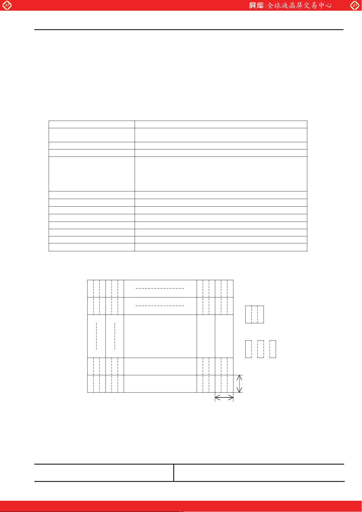
2.1 General Specifications
Item Specifications
Display Mode TN color(64 gray scales, 262,144 colors)
Viewing Direction 6 o'clock (in direction of maximum contrast)
Driving Method TFT active matrix
Input Signals LVDS interface
Active Area
Bezel Opening
Number of Pixels
Pixel Pitch
Pixel Arrangement RGB vertical stripes 1)
Surface Treatment Anti-glare and hard coat 3H on LCD surface
Backlight Single cold-cathode fluorescent lamp for sidelighting
Dimensional Outline
Note 1)
1 2 1023 1024
R G B
R G B
1
2
R G B
R G B
R G B
R G B
767
R G B
R G B
768
www.panelook.com
G050032-C971
Transmissive type, Normally white
CLK+,CLKIN0+,IN0IN1+,IN1IN2+,IN2-
245.76 (W) u 184.32 (H) (mm)
250.5 (W) u 188.9 (H) (mm)
1024 (W) u 768
0.240 (W) u 0.240 (H) (mm)
261.0 (W) u 199.0 (H) u 5.0max. (D) (mm)
(H)
R G B
R G B
R G B
R G B
0.279mm
1)
1)
R G B
R G B
R G B
R G B
R G B
R
G
0.279mm
Sheet 8
: pixel
: Sub-pixel
B
(Dots)
Toshiba Matsushita Display Technology Co.,Ltd
Date:2004-11-04 New No.NR-LTD121EC5V-11
Date: - - Old No.
m# Special m Addition m Change
One step solution for LCD / PDP / OLED panel application: Datasheet, inventory and accessory!
www.panelook.com
Page 10
Global LCD Panel Exchange Center
Specification No.
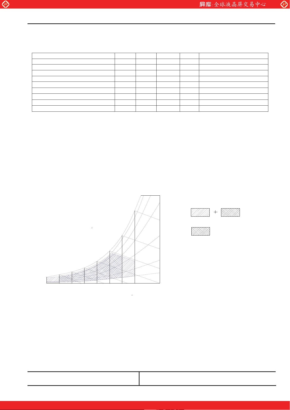
2.2 Absolute Maximum Ratings 1)
Item Symbol Min. Max. Unit Checked Terminal
Supply Voltage VDD -0.3 +4.0 V VDD - GND
Input Voltage of Signals VIN -0.3 VDD+0.3 V LVDS interface
FL Driving Voltage VFL - 2.0 kVrms
FL Driving Frequency fFL 0 100 kHz
Operating Ambient Temperature 2) TOP 0 +50
Operating Ambient Humidity 2) HOP 10 90 %(RH)
Storage Temperature 2) T
Storage Humidity 2) H
Operating Temperature for Panel 3) - 0 +60
Note1) Do not exceed the maximum rating values under the worst probable conditions taking into account the supply voltage
variation, input voltage variation, variation in part constants, and ambient temperature and so on. Otherwise the module
may be damaged.
2) Wet bulb temperature should be 39qC Max, and no condensation of water. See figure below.
3) The surface temperature caused by self heat radiation of cell itself is specified on this item.
4) Refer to 2.4.5
www.panelook.com
G050032-C971
qC
-20 +60
STG
10 90 %(RH)
STG
qC
qC
Sheet 9
4)
Wet Bulb
Temperature [ C]
30
20
10
0
0
-20 10 20 30 40 50 60 70 80
Dry Bulb Temperature [ C]
2.3 Mechanical Specifications
2.3.1 Weight
270 r 20 (g)
40
50
60
95%
80%
60%
40%
20%
10%
Storage
Operation
Humidity [%(RH)]
Toshiba Matsushita Display Technology Co.,Ltd
Date:2004-11-04 New No.NR-LTD121EC5V-11
Date: - - Old No.
m# Special m Addition m Change
One step solution for LCD / PDP / OLED panel application: Datasheet, inventory and accessory!
www.panelook.com
Page 11

Global LCD Panel Exchange Center
Specification No.
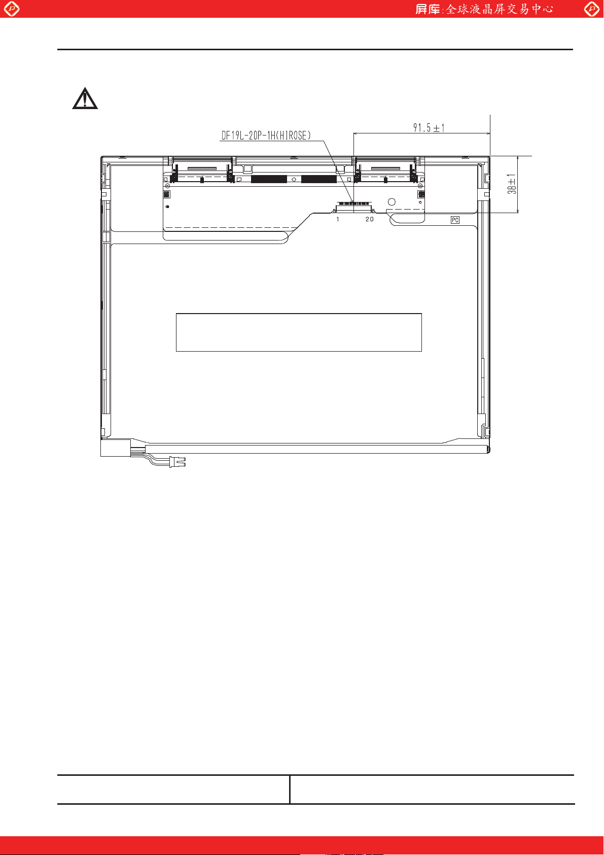
2.3.2 Dimensional Outline Unit : mm
(front figure) Standard Tolerance: r0.5
www.panelook.com
G050032-C971
Sheet 10
Note) If customer remove tape for fixing FL cable, Toshiba Matsushita Display Technology can not guarantee.
Toshiba Matsushita Display Technology Co.,Ltd
Date:2004-11-04 New No.NR-LTD121EC5V-11
Date: - - Old No.
m# Special m Addition m Change
One step solution for LCD / PDP / OLED panel application: Datasheet, inventory and accessory!
www.panelook.com
Page 12
Global LCD Panel Exchange Center
Specification No.
(Back figure)
Warning
www.panelook.com
G050032-C971
Sheet 11
Do Not Push rear side
Note 1) Never push LCD back side. If LCD back side was pressed, It may cause damage of the back light
system.
Toshiba Matsushita Display Technology Co.,Ltd
One step solution for LCD / PDP / OLED panel application: Datasheet, inventory and accessory!
Date:2004-11-04 New No.NR-LTD121EC5V-11
Date: - - Old No.
m# Special m Addition m Change
www.panelook.com
Page 13
(
)
Global LCD Panel Exchange Center
Specification No.
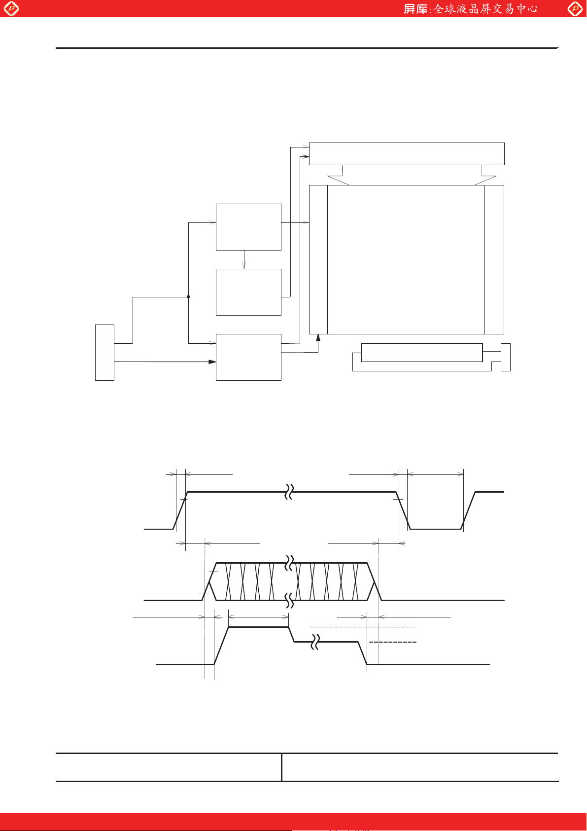
2.4 Electrical Specifications
2.4.1 Circuit Diagram
www.panelook.com
DC/DC
converter
G050032-C971
X-driver
Y-driver
Liquid Crystal Panel
Sheet 12
Y-driver
Gray scale
Manipulation
Voltage
Generation
CN1
Connector
Circuit
Panel
Controller
LVDS include
2.4.2 Sequence of Power Supplies and Signals
.
a
x
M
s
0
m
1
u
s
(
M
i
.
n
5
0
3
.
0
V
DD
V
0.2V
4
0
0
)
.
s
m
s
m
)
(
M
a
x
)
.
n
i
M
(
1024 x 768 pixels
Backlight
x
.
a
(
1
a
x
M
(
s
0
m
4
m
0
n
i
M
(
s
)
V
0
.
3
)
.
)
.
0
0
5
0.2V
s
m
M
m
s
0
)
.
n
i
M
(
0.2V
CN2
CLKIN0- - IN2-
CLK+
IN0+ - IN2+
1
m
0
10%
)
.
n
i
M
(
s
s
2
)
.
n
i
M
c
(
e
10%
m
0
)
.
n
i
M
(
s
V
L
S
F
V
L
F
Backlight
Toshiba Matsushita Display Technology Co.,Ltd
One step solution for LCD / PDP / OLED panel application: Datasheet, inventory and accessory!
Date:2004-11-04 New No.NR-LTD121EC5V-11
Date: - - Old No.
m# Special m Addition m Change
www.panelook.com
Page 14
Global LCD Panel Exchange Center
Specification No.
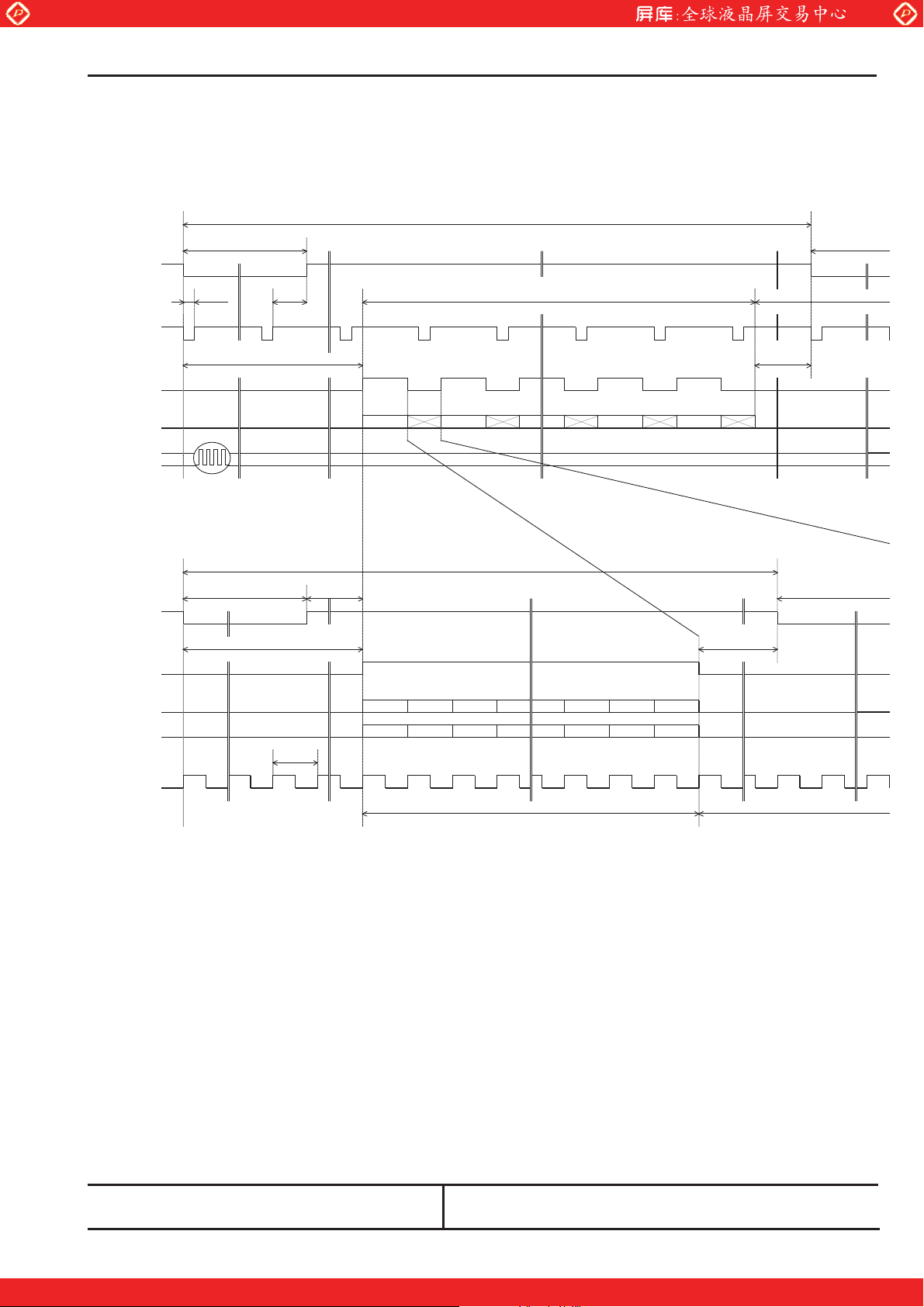
2.4.3 Timing Chart
(1) Vertical Timing
VSP W VSP W
VSYNC
tvsu tvhd VA VBL
HSYNC
Tvbp Tvfp
DE
www.panelook.com
G050032-C971
Tvp
Sheet 13
Data
CLK
(2) Horizontal Timing
HSYNC
DE
ODD-Data
EVEN-Data
CLK
X,1
HSPW ta HSPW
Thbp Thfp
1,Y 3,Y 5,Y 1019,Y 1021,Y 1023,Y
2,Y 4,Y 6,Y 1020,Y 1022,Y 1024,Y
Tc
X,2 X,767 X,76 8
Thp
HA HBL
Toshiba Matsushita Display Technology Co.,Ltd
Date:2004-11-04 New No.NR-LTD121EC5V-11
Date: - - Old No.
m# Special m Addition m Change
One step solution for LCD / PDP / OLED panel application: Datasheet, inventory and accessory!
www.panelook.com
Page 15
Global LCD Panel Exchange Center
Specification No.
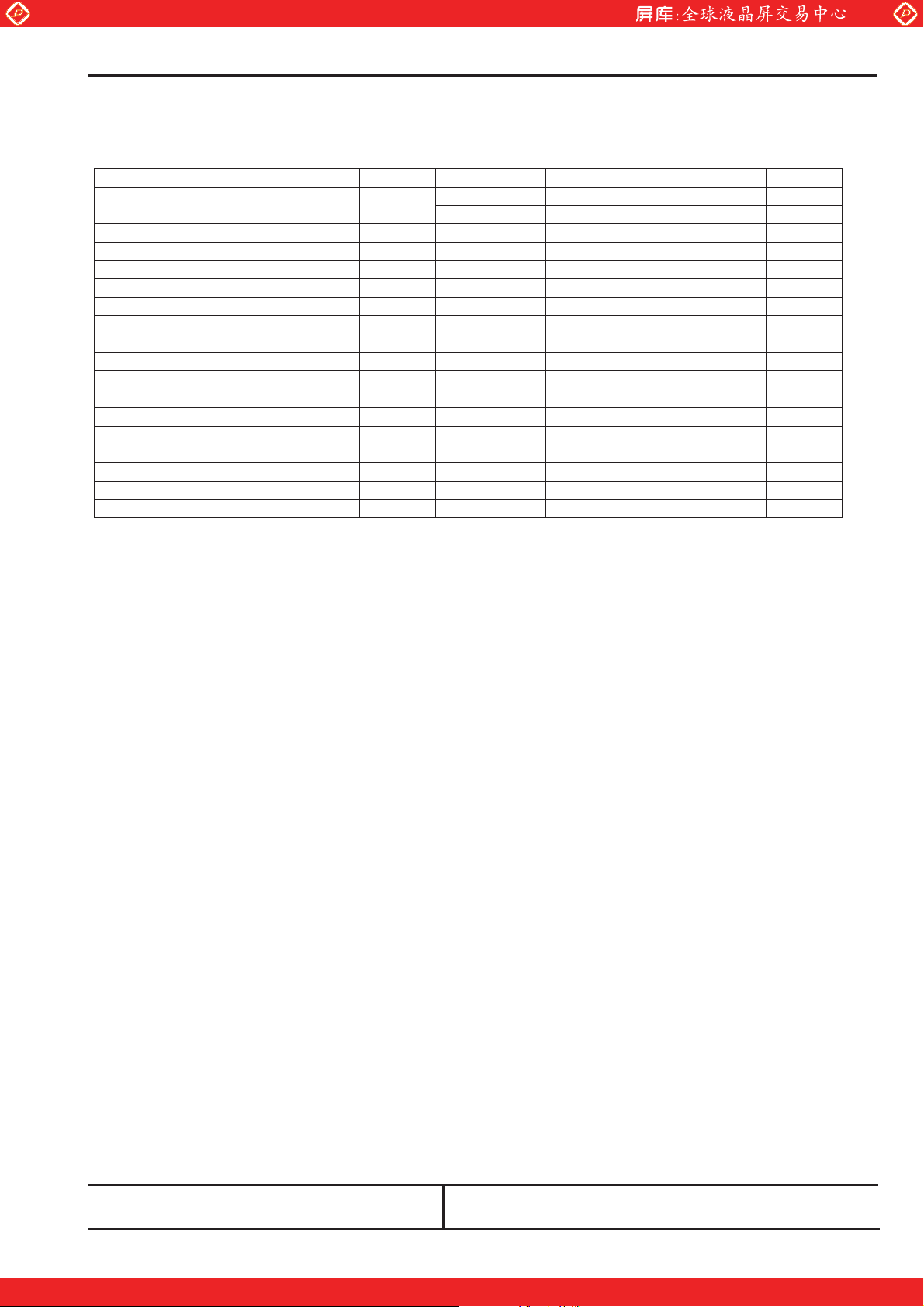
2.4.4 Timing Specifications
Item Symbol min. typ. max. unit
H-sync Pulse Width
Horizontal Front Porch thfp 4 - 136 Tc
Horizontal Back Porch ta 4 - 136 Tc
Horizontal Blanking Term
Horizontal Display Term
V-sync Pulse Width
V-sync Set Up Time (to H-sync) tvsu 8 - 14 Tc
V-sync Hold Time tvhd 8 - - Vertical Front Porch tvfp 2 - 8 Vertical Back Porch Tvbp 8 - 14 Vertical Blanking Term
Vertical Display Term
DE Pulse Width
Clock Period Tc 15.000 15.384 - ns
Note 1) Refer to “Timing Chart” and LVDS (THC63LVDF84A-85) specifications by THine Electronics, Inc.
Note 2) If CLK is fixed to "H" or "L" level for certain period while DE is supplied, the panel may be damaged.
Note 3) Please adjust LCD operating signal timing and FL driving frequency, to optimize the display quality.
There is a possibility that flicker is observed by the interference of LCD operating signal timing and FL driving condition
(especially driving frequency), even if the condition satisfies above timing specifications and recommended operating
conditions shown in 3.
Note 4) Do not make tv, th, thbp and tvds fluctuate.
If tv, th, thbp and tvds are fluctuate, the panel displays black.
Note 5) In case of using the long frame period, the deterioration of display quality, noise etc. may be occurred.
Note 6) CLK count of each Horizontal Scanning Time should be always the same.
V-Blanking period should be “n” X “Horizontal Scanning Time”. (n: integer)
Frame period should be always the same.
Note 7) Please keep below equations.
VBL = Tvfp + Tvbp
HSPW = HBL – Thfp – ta
Thbp = HSPW + ta
1) 2) 3) 4) 5) 6) 7)
HSPW
VSPW
www.panelook.com
G050032-C971
Th
HBL
HA
Tvp
VBL
VA
HA
1334 1344 1462 Tc Horizontal Scanning Term
- 20.68 - us
12 - 140 Tc
295 320 438 Tc
1024 1024 1024 Tc
778 806 860 Thp Frame Period
- 16.67 17.24 ms
2 - 7 Thp
10 38 92 Thp
768 768 768 Thp
1024 1024 1024 Tc
Sheet 14
Toshiba Matsushita Display Technology Co.,Ltd
Date:2004-11-04 New No.NR-LTD121EC5V-11
Date: - - Old No.
m# Special m Addition m Change
One step solution for LCD / PDP / OLED panel application: Datasheet, inventory and accessory!
www.panelook.com
Page 16
Global LCD Panel Exchange Center
Specification No.
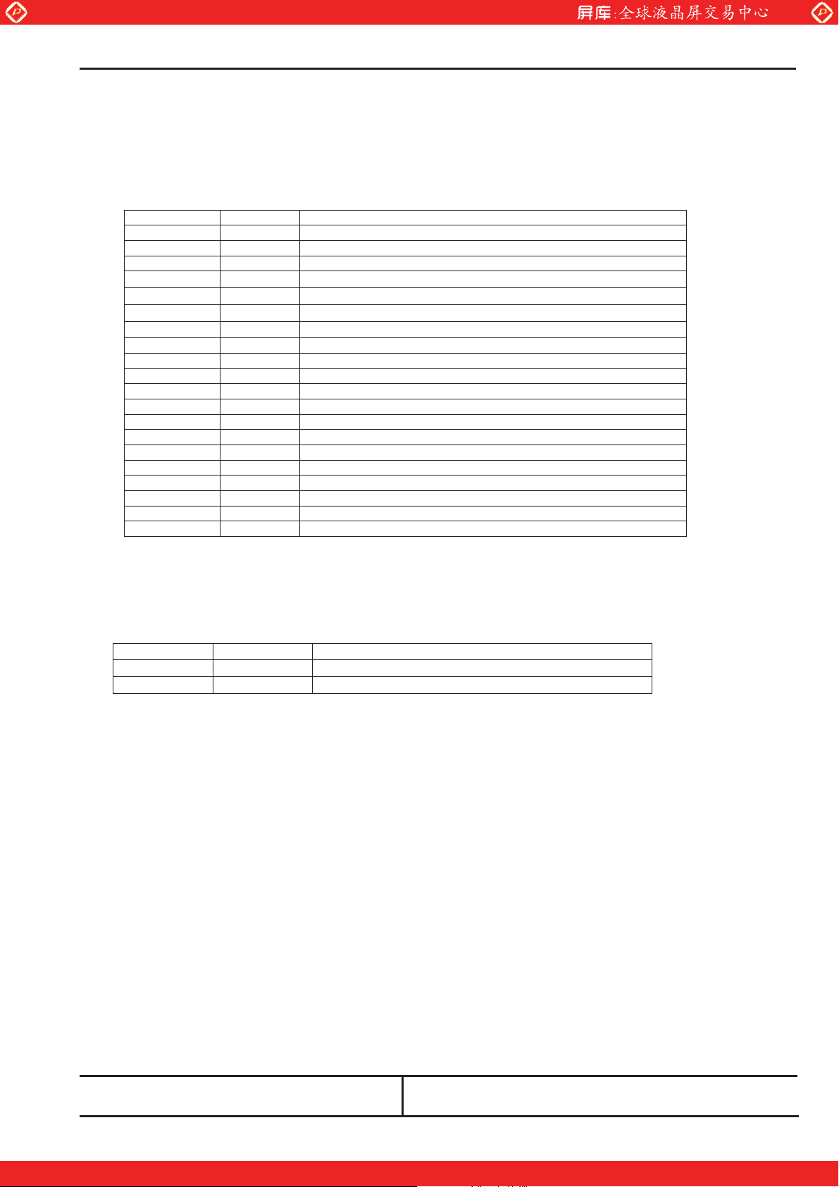
2.4.5 Interface Connector
CN1 INPUT SIGNAL (DF19L-20P-1H / HIROSE )
[ Mating Connector : DF19G-20S-1C (Cable),
DF19G-20S-1F (FRC Type) / HIROSE ]
Terminal No. Symbol Function
1
2
3
4
5
6
7
8 RxIN0- Negative LVDS differential data input (R0-R5,G0)
9 RxIN0+ Positive LVDS differential data input (R0-R5,G0)
10
11 RxIN1- Negative LVDS differential data input (G1-G5, B0-B1)
12 RxIN1+ Positive LVDS differential data input (G1-G5, B0-B1)
13
14 RxIN2- Negative LVDS differential data input (B2-B5, HS, VS, DE)
15 RxIN2+ Positive LVDS differential data input (B2-B5, HS, VS, DE)
16
17 CLK- Clock Signal(-)
18 CLK+ Clock Signal(+)
19
20
Note 1) Please connect GND pin to ground. Don't use it as no-connect nor connectiton with high impedance.
CN2 CCFL POWER SOURCE (BHTR-02VS-1/JAPAN SOLDERLESS TERMINAL MFG CO., LTD.)
[ Mating Connector : SM02B-BHTS-1/JAPAN SOLDERLESS TERMINAL MFG CO., LTD. ]
Terminal No. Symbol Function
1 V
2 V
Note 2) 262,144 colors are displayed by the combinations of 18 bits data. (See next page)
SS
V
DD
V
DD
V
V
DDC 3.3V POWER SUPPLY : +3.3V
EDID
NC Non-Connection
CLK
EDID
DATA
EDID
SS
V
SS
V
SS
V
SS
V
SS
V
CCFL POWER SUPPLY (HIGH VOLTAGE)
FLH
CCFL POWER SUPPLY (LOW VOLTAGE)
FLL
www.panelook.com
GND
Power Supply : +3.3V
Power Supply : +3.3V
DDC Clock
DDC Data
GND
GND
GND
GND
GND
G050032-C971
Sheet 15
Toshiba Matsushita Display Technology Co.,Ltd
Date:2004-11-04 New No.NR-LTD121EC5V-11
Date: - - Old No.
m# Special m Addition m Change
One step solution for LCD / PDP / OLED panel application: Datasheet, inventory and accessory!
www.panelook.com
Page 17
Global LCD Panel Exchange Center
Specification No.
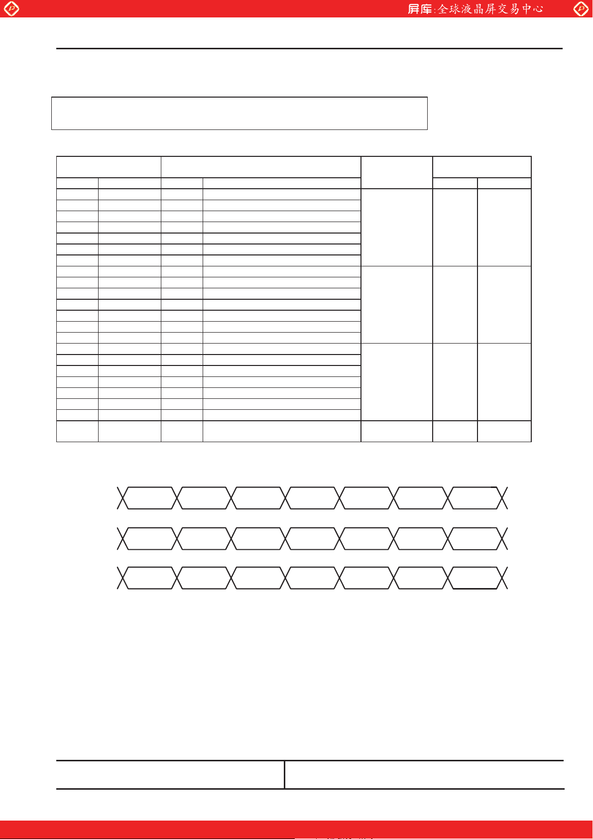
RECOMMENDED TRANSMITTER TRANSMITTER (THC63LVDF83A,THC63LVDM83A,THC63LVDM83A-85)
TO LTD121EC5V INTERFACE ASSIGNMENT
Case1: 6Bit TRANSMITTER
Input Terminal No. Input Signal
(Graphics controller output signal)
Symbol Terminal Symbol Function
TIN0 44 R0 Red Pixels Display Data (LSB)
TIN1 45 R1 Red Pixels Display Data
TIN2 47 R2 Red Pixels Display Data
TIN3 48 R3 Red Pixels Display Data
TIN4 1 R4 Red Pixels Display Data
TIN5 3 R5 Red Pixels Display Data (MSB)
TIN6 4 G0 Green Pixels Display Data (LSB)
TIN7 6 G1 Green Pixels Display Data
TIN8 7 G2 Green Pixels Display Data
TIN9 9 G3 Green Pixels Display Data
TIN10 10 G4 Green Pixels Display Data
TIN11 12 G5 Green Pixels Display Data (MSB)
TIN12 13 B0 Blue Pixels Display Data (LSB)
TIN13 15 B1 Blue Pixels Display Data
TIN14 16 B2 Blue Pixels Display Data
TIN15 18 B3 Blue Pixels Display Data
TIN16 19 B4 Blue Pixels Display Data
TIN17 20 B5 Blue Pixels Display Data (MSB)
TIN18 22 HSYNC H-Sync
TIN19 23 VSYNC V-Sync
TIN20 25 DE Compound Synchronization Signal
CLK IN 26 NCLK Data Sampling Clock TCLK OUT-
www.panelook.com
G050032-C971
Output Signal
Symbol
TOUT0TOUT0+
TOUT1TOUT1+
TOUT2TOUT2+
TCLK OUT+
Sheet 16
To LT D 1 2 1 E C5 V
Interface(CN1)
Terminal Symbol
No.8
No.9
No.11
No.12
No.14
No.15
No.17
No.18
RxIN0RxIN0+
RxIN1RxIN1+
RxIN2RxIN2+
CLK INCLK IN+
IN 0
IN 1
IN 2
TIN6
G0
TIN13
B1
TIN20
DE
TIN5
R5
T IN 1 2 T IN 1 1 T IN 1 0 T IN 9 T IN 8
B0
T IN19 T IN18 T IN17 T IN16 T IN15
VSYNC
TIN4 TIN3 TIN2 TIN1 TIN0
R4
G5
HSYNC
Toshiba Matsushita Display Technology Co.,Ltd
R3 R2 R1 R0
TIN7
G4
B5
G3
B4
G2
G1
TIN14
B2B3
Date:2004-11-04 New No.NR-LTD121EC5V-11
Date: - - Old No.
m# Special m Addition m Change
One step solution for LCD / PDP / OLED panel application: Datasheet, inventory and accessory!
www.panelook.com
Page 18
Global LCD Panel Exchange Center
Specification No.
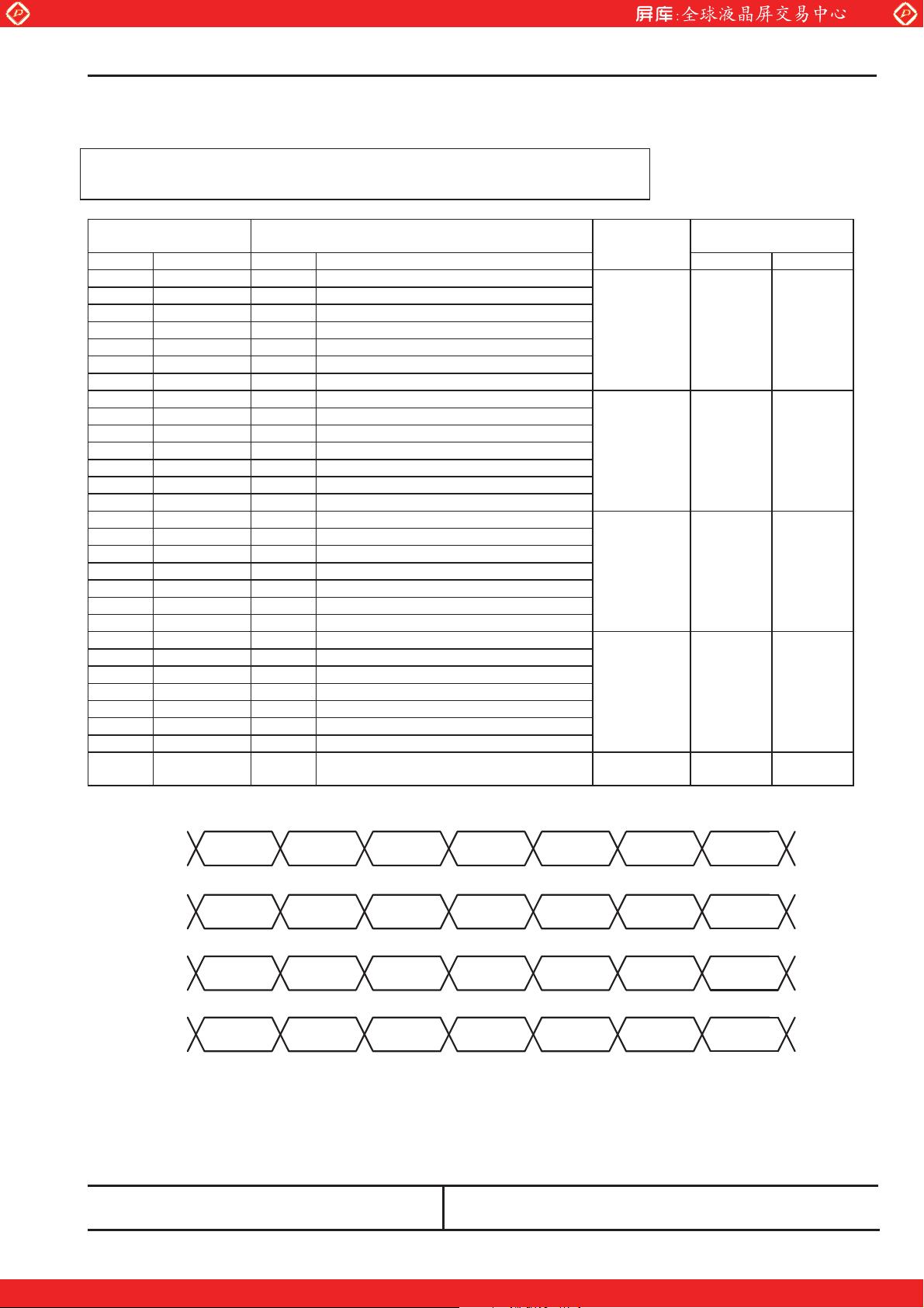
RECOMMENDED TRANSMITTER (THC63LVDF83A,THC63LVDM83A,THC63LVDM83A-85)
TO LTD121EC5V INTERFACE ASSIGNMENT
Case2: 8Bit TRANSMITTER
Input Terminal No. Input Signal
Symbol Terminal Symbol Function
TIN0 51 R0 Red Pixels Display Data (LSB)
TIN1 52 R1 Red Pixels Display Data
TIN2 54 R2 Red Pixels Display Data
TIN3 55 R3 Red Pixels Display Data
TIN4 56 R4 Red Pixels Display Data
TIN5 3 R5 Red Pixels Display Data (MSB)
TIN6 4 G0 Green Pixels Display Data(LSB)
TIN7 6 G1 Green Pixels Display Data
TIN8 7 G2 Green Pixels Display Data
TIN9 11 G3 Green Pixels Display Data
TIN10 12 G4 Green Pixels Display Data
TIN11 14 G5 Green Pixels Display Data(MSB)
TIN12 15 B0 Blue Pixels Display Data (LSB)
TIN13 19 B1 Blue Pixels Display Data
TIN14 20 B2 Blue Pixels Display Data
TIN15 22 B3 Blue Pixels Display Data
TIN16 23 B4 Blue Pixels Display Data
TIN17 24 B5 Blue Pixels Display Data (MSB)
TIN18 27 HSYNC H-Sync
TIN19 28 VSYNC V-Sync
TIN20 30 DE Compound Synchronization Signal
TIN21 50 NC Non Connection (open)
TIN22 2 NC Non Connection (open)
TIN23 8 NC Non Connection (open)
TIN24 10 NC Non Connection (open)
TIN25 16 NC Non Connection (open)
TIN26 18 NC Non Connection (open)
TIN27 25 NC Non Connection (open)
CLK IN 31 NCLK Data Sampling Clock TCLK OUT-
www.panelook.com
G050032-C971
(Graphics controller output signal)
Output
Signal
Symbol
TOUT0TOUT0+
TOUT1TOUT1+
TOUT2TOUT2+
TOUT3TOUT3+
TCLK OUT+
Sheet 17
To LT D 1 2 1 E C5 V
Interface(CN1)
Terminal Symbol
No.8
No.9
No.11
No.12
No.14
No.15
-
No.17
No.18
RxIN0RxIN0+
RxIN1RxIN1+
RxIN2RxIN2+
-
CLK INCLK IN+
IN0
IN1
IN2
IN3
G0
B1
TIN20
DE
NC
TIN5TIN6
R5
B0
NC
TIN4 TIN3 TIN2 TIN1 TI N0
R4
G5
HSYNCVSYNC
NC
R3 R2 R1 R0
TIN7
TIN14
TIN21TIN22TIN23TIN24TIN25TIN26TIN27
G4
B5
NC
G3
B4
NC
TIN8TIN9TIN10TIN11TIN12TIN1 3
G2
TIN15TIN16TIN17TIN18TIN19
NC
Toshiba Matsushita Display Technology Co.,Ltd
Date:2004-11-04 New No.NR-LTD121EC5V-11
Date: - - Old No.
m# Special m Addition m Change
One step solution for LCD / PDP / OLED panel application: Datasheet, inventory and accessory!
G1
B2B3
NC
www.panelook.com
Page 19
Global LCD Panel Exchange Center
Specification No.
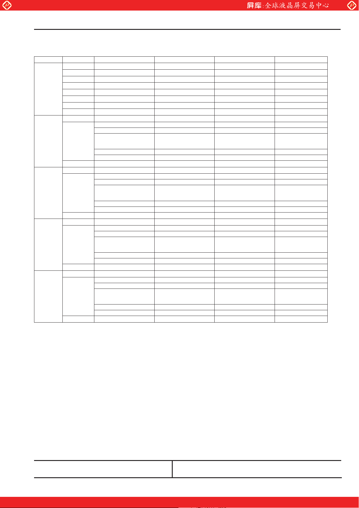
2.4.6 Colors Combination Table
Display
Basic
Color
Gray
Scale of
Red
Gray
Scale of
Green
Gray
Scale of
Blue
Gray
Scale of
White &
Black
Black
Blue
Green
Light Blue
Red
Purple
Yell ow
White
Black
Dark
n
p
Light
Red
Black
Dark
n
p
Light
Green
Black
Dark
n
p
Light
Blue
Black
Dark
n
p
Light
White
Note1 L: Low level voltage, H: High level voltage
R5 R4 R3 R2 R1 R0 G5 G4 G3 G2 G1 G0 B5 B4 B3 B2 B1 B0
L L L L L L L L L L L L L L L L L L L L L L L L L L L L L L H H H H H H L L L L L L H H H H H H L L L L L L L L L L L L H H H H H H H H H H H H H H H H H H L L L L L L L L L L L L H H H H H H L L L L L L H H H H H H H H H H H H H H H H H H L L L L L L H H H H H H H H H H H H H H H H H H L L L L L L L L L L L L L L L L L L L 0
L L L L L H L L L L L L L L L L L L L 1
L L L L H L L L L L L L L L L L L L L 2
H H H H L H L L L L L L L L L L L L L61
H H H H H L L L L L L L L L L L L L L62
H H H H H H L L L L L L L L L L L L Red L63
L L L L L L L L L L L L L L L L L L L 0
L L L L L L L L L L L H L L L L L L L 1
L L L L L L L L L L H L L L L L L L L 2
L L L L L L H H H H L H L L L L L L L61
L L L L L L H H H H H L L L L L L L L62
L L L L L L H H H H H H L L L L L L Green L63
L L L L L L L L L L L L L L L L L L L 0
L L L L L L L L L L L L L L L L L H L 1
L L L L L L L L L L L L L L L L H L L 2
L L L L L L L L L L L L H H H H L H L61
L L L L L L L L L L L L H H H H H L L62
L L L L L L L L L L L L H H H H H H Blue L63
L L L L L L L L L L L L L L L L L L L 0
L L L L L H L L L L L H L L L L L H L 1
L L L L H L L L L L H L L L L L H L L 2
H H H H L H H H H H L H H H H H L H L61
H H H H H L H H H H H L H H H H H L L62
H H H H H H H H H H H H H H H H H H White L63
:
:
:
:
:
:
:
:
www.panelook.com
G050032-C971
:
:
:
:
:
:
:
:
:
:
:
:
:
:
:
:
Sheet 18
Gray ScaleLevel
L 3 }
L 6 0
L 3 }
L 6 0
L 3 }
L 6 0
L 3 }
L 6 0
Toshiba Matsushita Display Technology Co.,Ltd
Date:2004-11-04 New No.NR-LTD121EC5V-11
Date: - - Old No.
m# Special m Addition m Change
One step solution for LCD / PDP / OLED panel application: Datasheet, inventory and accessory!
www.panelook.com
Page 20
Global LCD Panel Exchange Center
Specification No.
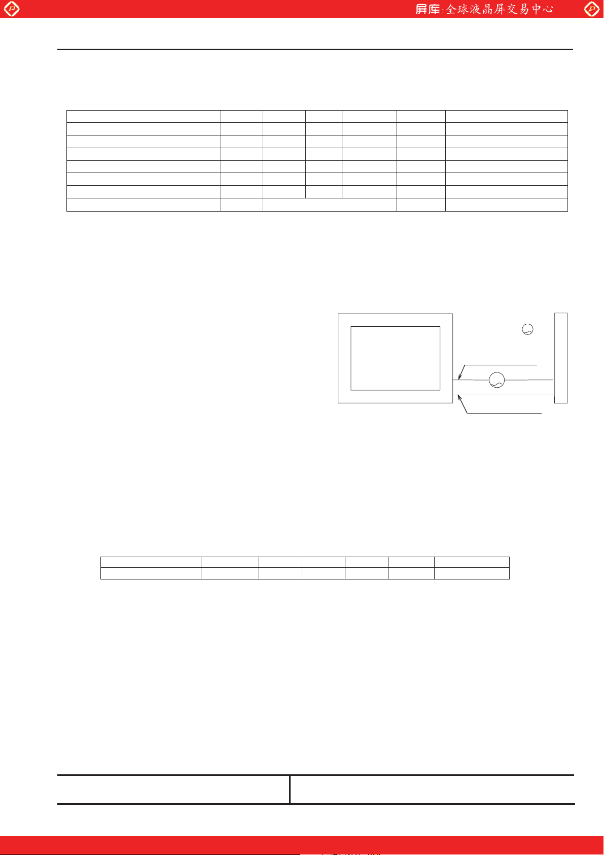
3. Recommended Operating Conditions
Item Symbol Min. Typ. Max. Unit Remarks
Supply Voltage 4) VDD 3.0 3.3 3.6 V
Differential Input Voltage VID 100 - 600 mV
Comon Mode Input Voltage VCM 1.0 - 2.4-(VID)/2 V
FL Input Current
FL Driving Voltage 6) VFL 575 625 675 V(rms) IFL=6.0mA(rms)(Reference)
FL Driving Frequency 6) fFL 30 50 80 kHz
FL Starting Voltage
Note 1) The module should be always operated within these ranges. The "Typ." shows the recommendable value.
2) Recommended LVDS transmitter: THC63LVDF63A, THC63LVDM63A, THC63LVDM63A-85, THC63LVDF83A,
THC63LVDM83A,THC63LVDM83A-85 (made by THine Electronics,Inc.)
Panel Controller contains LVDS, which is based on THC63LVDF84A-85 (made by THine Electronics,Inc.)
specification.
3) Checked Pin Terminal: V
4) Checked Pin Terminal: IN0-㨪CLK+, GND (0V)
Measure:~V
~V
Measure: (V
(V
5) Checked Pin Terminal: V
6) If FL input current (I
value(6.0mA(rms)), then FL lifetime becomes shorter.
7) Measuring Method of I
8) Input FL starting voltage (V
If it were less than two second, it may cause unstable operation of FL.
9) Please adjust LCD operating signal timing and FL driving frequency, to optimize the display quality.
There is a possibility that flicker is observed by the interference of LCD operating signal timing and FL driving condition
(especially driving frequency), even if the condition satisfies above recommended operating conditions and timing
specifications shown in 2.4.4.
10) Inverter open voltage should not be less than 1400V(rms).
Symbol Min. Typ. Max. Unit Oters
6) 7) 8)
IFL 2.0 - 6.0 mA(rms)
6) 9)
V
DD
IN0+-VIN0-~, ~VIN1+-VIN1-~, ~VIN2+-VIN2-~
CLKN+-VCLK-~
IN0+-VIN0-)/2, (VIN1+-VIN1-)/2,
IN2+-VIN2-)/2, (VCLK++-VCLK-)/2,
FLH
) is higher than typical
FL
.
FL
FL starting Voltage V
www.panelook.com
G050032-C971
1) 2) 3) 10)
SFL
, GND (0V)
- F
FLL
) should not be less than two second.
SFL
- - 1400 V(rms)
SFL
10)
V(rms)
TFT Module
0qC
Sheet 19
0qC
:AC ampere meter
VFLH:High Voltage Line
A
A
VFLL:Low Voltage Line
L Inverter
F
Toshiba Matsushita Display Technology Co.,Ltd
Date:2004-11-04 New No.NR-LTD121EC5V-11
Date: - - Old No.
m# Special m Addition m Change
One step solution for LCD / PDP / OLED panel application: Datasheet, inventory and accessory!
www.panelook.com
Page 21
Global LCD Panel Exchange Center
Specification No.
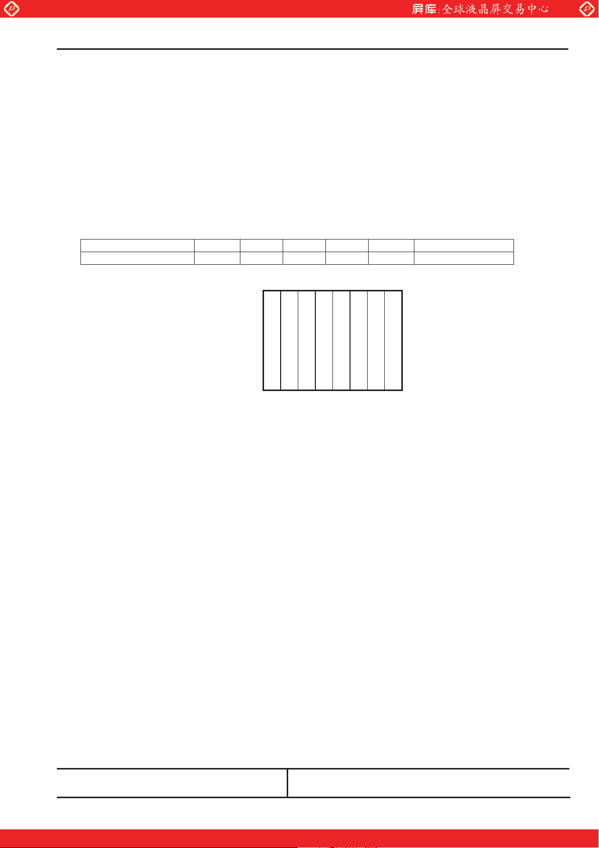
4. Electrical Characteristics
4.1 Test Conditions
Ambient Temperature : T
Ambient Humidity : H
Supply Voltage : V
Input Signal : Refer typical value in "2.4.4 Timing Specifications".
FL Input Current : I
FL Driving Frequency : f
4.2 Specifications
Item Symbol Min. Typ.
Current Consumption IDD - 215 400 mA VDD Terminal Current
Note 1) The Typical value of IDD is measured in the following pattern.
1. White
2. Yellow
3. Purple
4. Red
5. Light Blue
6. Green
7. Blue
6. Black
www.panelook.com
25r5qC
a
65r20%(RH)
a
3.3V
DD
6.0mA(rms)
FL
50kHz
FL
G050032-C971
1)
Max. Unit Remark
13245678
Sheet 20
Toshiba Matsushita Display Technology Co.,Ltd
Date:2004-11-04 New No.NR-LTD121EC5V-11
Date: - - Old No.
m# Special m Addition m Change
One step solution for LCD / PDP / OLED panel application: Datasheet, inventory and accessory!
www.panelook.com
Page 22
Global LCD Panel Exchange Center
Specification No.
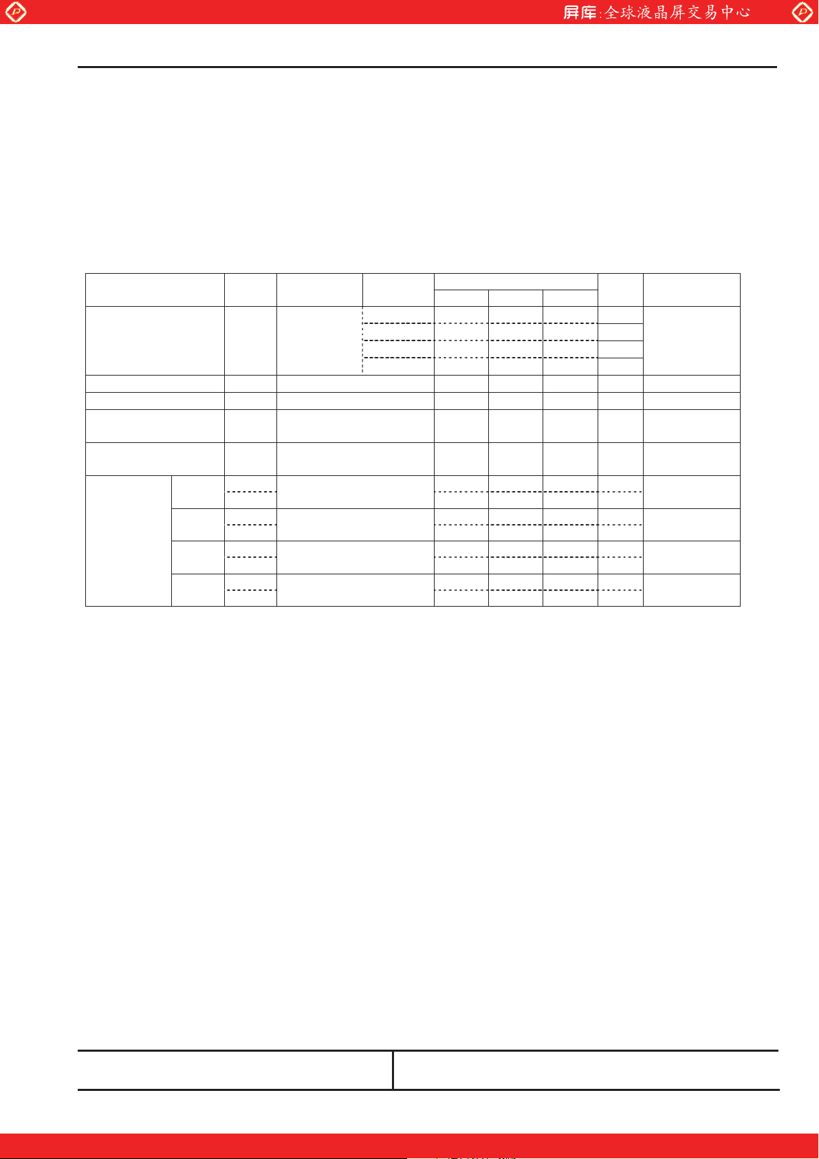
5. Optical Characteristics
5.1 Test Conditions
It is same as 4.1
The measuring method is shown in 11.
5.2 Optical Specifications 1)
Item Symbol Conditions
Viewing Angle
Contrast Ratio
Response Time tON+t
Luminance
Luminance Uniformity2) LUNF
Chromaticity
White
Note 1): Refer to "11. Measuring Method".
Note 2): The above test limit must be applied for initial use. Characteristics will be shifted by long period operation, but it is not
irregular phenomena. Theoretically brightness characteristics will be decreased due to CCFL degradation and color
shift due to optical components change.
T
CR
OFF
L
xR 0.550 0.600 0.650 - Red
y
R
xG 0.245 0.295 0.345 - Green
y
G
xB 0.100 0.150 0.200 - Blue
y
B
xW 0.273 0.313 0.343 y
W
www.panelook.com
CR>=10
T
=0q, I =0q
T
=0q, I =0q
T
=0q, I =0q Gray Scale
Level=L63 (White)
T
=0q, I =0q Gray Scale
Level=L63 (White)
Gray Scale Level:L63
T
=0q, I =0q
Ditto
Ditto
Ditto
I
= 180q
I
= 0q
I
= 90q
I
= -90q
G050032-C971
Specifications
MIn. Typ Max.
10 - 20 - 30 - 30 - -
150 - - -
- - 50 ms
150 180 - cd/m
- - 1.6 % Lmax / Lmin
0.278 0.328 0.378 -
0.483 0.533 0.583 -
0.075 0.125 0.175 -
0.289 0.329 0.369 -
Sheet 21
Unit Remark
q
q
q.
q
2
IFL=6.0mA(rms)
5point
Toshiba Matsushita Display Technology Co.,Ltd
Date:2004-11-04 New No.NR-LTD121EC5V-11
Date: - - Old No.
m# Special m Addition m Change
One step solution for LCD / PDP / OLED panel application: Datasheet, inventory and accessory!
www.panelook.com
Page 23
Global LCD Panel Exchange Center
Specification No.
6.Quality
6.1 Inspection AQL
Total of Major Defects : AQL 0.65 %
Total of Minor Defects : AQL 1.5 %
Sampling Method : ANSI / ASQC Z1.4 (Level ll)
6.2 Test Conditions
1) Ambient Temperature : 25r5qC
2) Ambient Humidity : 65r20%(RH)
3) Illumination : Approximately 500 lx under the fluorescent lamp
4) Viewing Distance : Approximately 30cm by the eyes of the inspector from the module
5) Inspection Angle :
6.3 Dimensional Outline
The products shall conform to the dimensions specified in 2.3.2.
Definition of Major and Minor defects are as follows.
Item Description Class
Important Dimensions Dimensional outline, Dimensional between
the mounting holes(hinge)
Others Dimensions specified in this specifications Minor
www.panelook.com
T
=0q, I =0q
G050032-C971
Sheet 22
Major
Toshiba Matsushita Display Technology Co.,Ltd
Date:2004-11-04 New No.NR-LTD121EC5V-11
Date: - - Old No.
m# Special m Addition m Change
One step solution for LCD / PDP / OLED panel application: Datasheet, inventory and accessory!
www.panelook.com
Page 24
Global LCD Panel Exchange Center
Specification No.
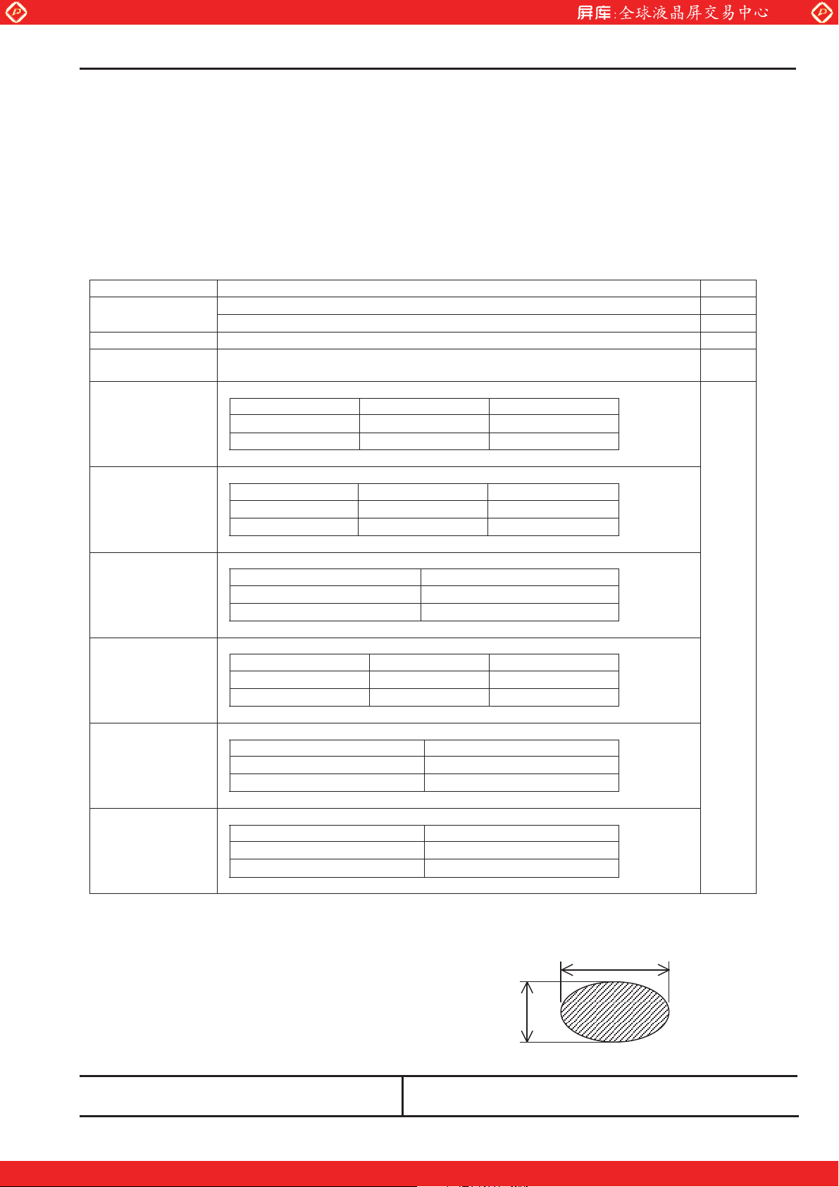
6.4 Appearance Test
6.4.1 Test Conditions
1) Condition : Non-operating, operating (Pattern : L63 white raster)
Same as 6.2
6.4.2 Specifications
Item Description Class
Pattern peeling snapping, electrically short Major PCB Appearance
Repair portion on PCB is not covered by epoxy resign Minor
Soldering Cold solder joint, lead move when pulled Major
Bezel, Frame,
Connectors
Bright Lines
(Light Lint)
Dark Lines
(Dark Lint/Hair)
Black and White
Spots
Polarizer Scratch1)
Polarizer Dents
Polarizer Bubble
Note 1) Inspection area should be within active area
Note 2) Black/White Spot, Polarizer Dents and Polarizer Bubble shall be judged by "Average Diameter".
Average Diameter D = (a+b) /2 (mm)
1)2)
1)
1)
Distinct stain, rust or scratch Minor
Line width(mm) Length(mm) Acceptable count
0.03 W d 0.152 L d 2.03 n d 4
0.152 W 2.03 L
Line width(mm) Length(mm) Acceptable count
0.03 W d 0.1 0.3 L d 1.0 n d 4
0.1 W 1.0 L
Average diameter(mm) Acceptable count/side
0.25 D d 0.4 n d 3
0.4 D
Line width(mm) Length(mm) Acceptable count
0.01 W d 0.05 1.0 L d 10.0 n d 3
0.05 W 10 .0 L
1)2)
1)2)
Average diameter(mm) Acceptable count
0.127 D d 0.38 n d 3
0.38 D
Average diameter(mm) Acceptable count
0.254 D d 0.38 n d 3
0.38 D
www.panelook.com
G050032-C971
0
0
0
0
0
Sheet 23
0
Minor
a
b
Toshiba Matsushita Display Technology Co.,Ltd
One step solution for LCD / PDP / OLED panel application: Datasheet, inventory and accessory!
Date:2004-11-04 New No.NR-LTD121EC5V-11
Date: - - Old No.
m# Special m Addition m Change
www.panelook.com
Page 25
Global LCD Panel Exchange Center
Specification No.
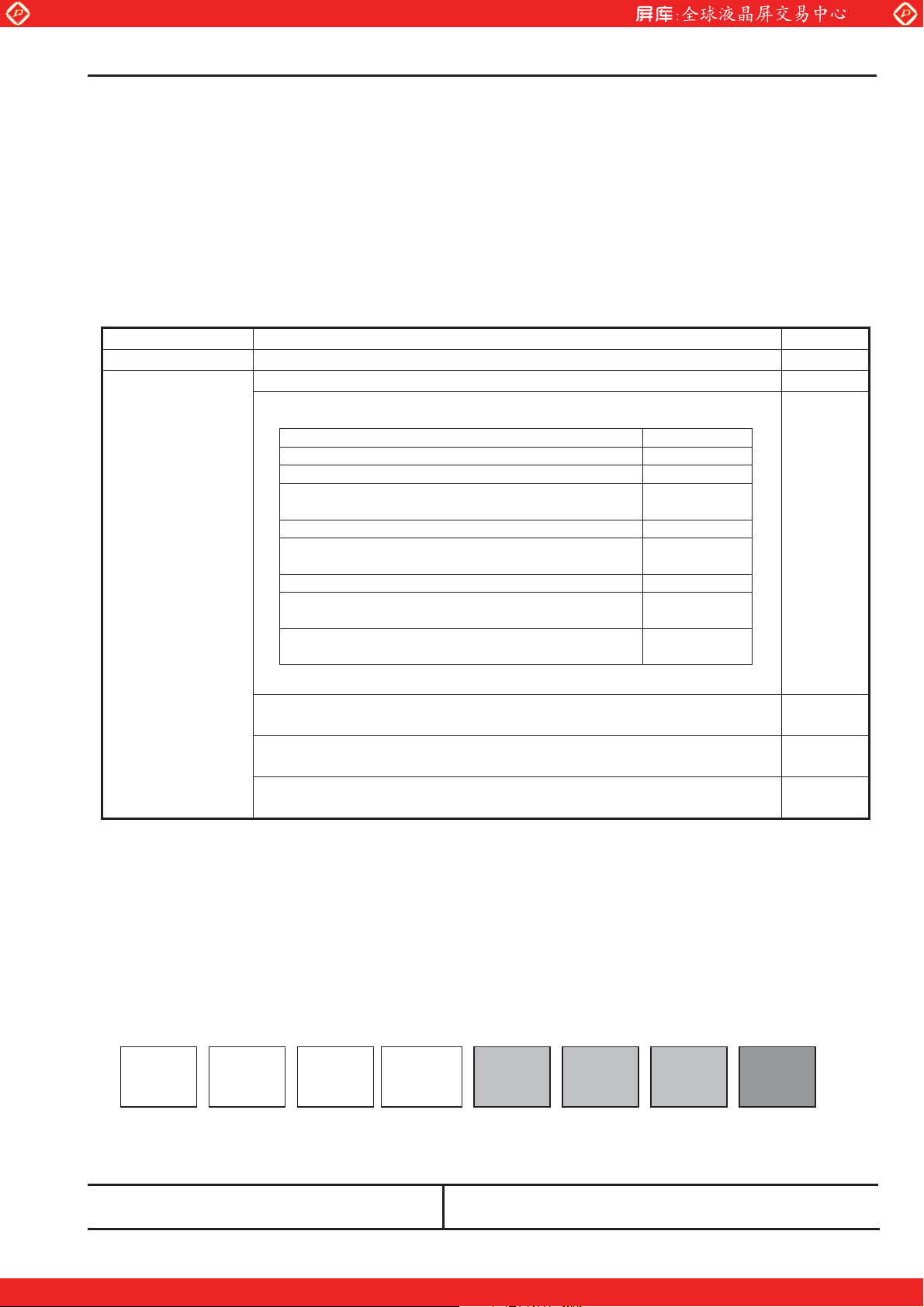
6.5 Display Quality
6.5.1 Test Conditions
1) Inspection Area : Within active area
2) Driving Condition : Same as test conditions shown in 4.1 and 6.2
3) Test Pattern : White display pattern (gray scale level L63) and black display pattern (gray scale level L0)
6.5.2 Specifications
Item Description / Specifications Class
Function No display, Malfunction Major
Display Quality 1)
Note 1) Defects of both color filter and black matrix are counted as bright or dark defects.
Inspection area should be within the active area.
Note 2) Bright defect means a bright spot(sub-pixel) on the display pattern of gray scale L0.
Dark defect means a dark spot(sub-pixel) on the display pattern of gray scale L63.
Note 3) Bright defect visible through the 2% ND-Filter are to be considered high level defects.
Those visible through the 5% ND-Filter are to be considered low level defects..
Note 4) Testing is conducted only on RED, GREEN, BLUE, WHITE of gray scale L63, RED, GREEN, BLUE of gray scale
L31,and BLACK of gray scale L0.
4)
Missing line Major
Missing Sub-Pixels
1) Red and Blue Bright (High and Low) defects
2) Green bright (High and Low) defects
3) Dark defects
4) Green high bright defect to
green high bright defect distance
5) High bright defect to high bright defect distance -
6) High bright defect to low bright defect and
low bright defect to low bright defect distance
7) Dark defect to dark defect distance 25mm min.
8) Low bright defect conjunction
(2 sub-pixels)
9) Dark defect conjunction
(2 sub-pixels)
Inconspicuous flicker, crosstalk, Newton's ring, Mottling Rubbing defect,
Dim Lines, Horizontal Line and Vertical Line. : neglect
Minimum distance between ANY allowable defect 5)
: 25.4mm min.
Maximum number of ALL allowable defects
: 7pcs. max.
www.panelook.com
G050032-C971
2)3)4)5)6)
2)3)4)5)6)
2)4)
3pcs. max.
1pcs. max.
0pcs. max.
Sheet 24
Major
-
-
0 sets max.
1sets max.
Major
Major
Major
RED
L63
Note 5) Toshiba Matsushita Display counts minimum distance between ANY allowable defects on white L63 screen only.
GREEN
L63
BLUE
L63
WHITE
L63
RED
L31
GREEN
L31
BLUE
L31
Toshiba Matsushita Display Technology Co.,Ltd
Date:2004-11-04 New No.NR-LTD121EC5V-11
Date: - - Old No.
m# Special m Addition m Change
One step solution for LCD / PDP / OLED panel application: Datasheet, inventory and accessory!
BLACK
L0
www.panelook.com
Page 26
Global LCD Panel Exchange Center
Specification No.
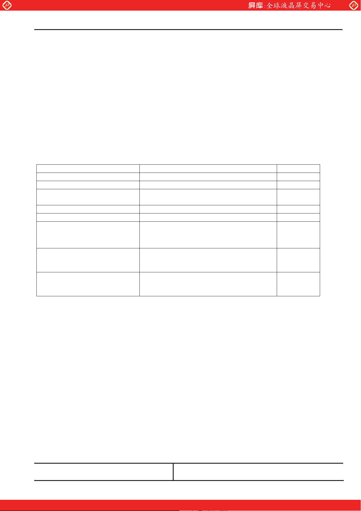
6.6 Reliability Test
6.6.1 Test Conditions
1) The module should be driven and inspected under normal test conditions.
2) The module should not have condensation of water (moisture) on the module.
3) The module should be inspected after two or more hours storage in normal conditions (15 - 35qC, 45 - 65%(RH)).
4) A module shall be used only for one test.
6.6.2 Specifications
The module shall have no failure in the following reliability test items.
Test Item Test Conditions Result
High Temperature Operation 1) 50qC 192 h OK 3p/3p
High Temperature Storage 2) 60qC 192 h OK 3p/3p
High Temperature and
High Humidity operation
Low Temperature Operation 1) 0qC 192 h OK 3p/3p
Low Temperature Storage 2) -20qC 192 h OK 3p/3p
Temperature Shock 2) -20qC 60qC
1)
www.panelook.com
G050032-C971
50qC 80% 192 h OK 3p/3p
0.5h 0.5h
50 cycles
Sheet 25
OK 3p/3p
Mechanical Vibration 2) 10 – 200 - 10Hz sweep/cycle,
1.5u9.8m/s
X.Y.Z each direction, 0.5h each
Mechanical Shock 2) 50u9.8m/s2 , 20ms,
rX, rY, rZ each direction,
one time each
Note 1) Operating
Note 2) Non-Operating
Definitions of failure for judgment shall be as follows:
1) Function of the module should be maintained.
2) Current consumption should be smaller than the specified value.
3) Appearance and display quality should not have distinguished degradation.
4) Luminance should be larger than 50% of the minimum value specified in 5.2.
2
constant,
OK 3p/3p
OK 3p/3p
Toshiba Matsushita Display Technology Co.,Ltd
Date:2004-11-04 New No.NR-LTD121EC5V-11
Date: - - Old No.
m# Special m Addition m Change
One step solution for LCD / PDP / OLED panel application: Datasheet, inventory and accessory!
www.panelook.com
Page 27
Global LCD Panel Exchange Center
Specification No.
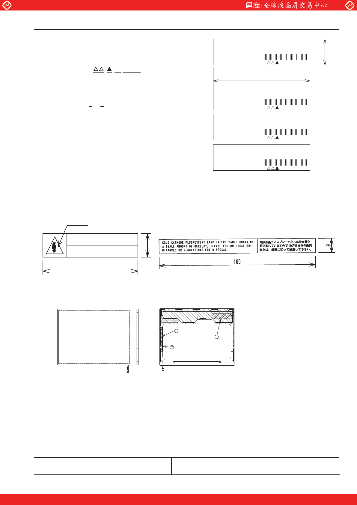
6.7 Labels
(1) Product Label
Serial number : 4A 000001
c
c : Module type code
d : Manufacturing code
e : Lot code 4
(1) (2)
(1):Year code-end of the A.D.
(2):Month code-alphabetÆ Jan. : A - Dec. : L
(Example: 4AÆ2004 JAN.)
f:Serial code
decimal, 6 figures
Bar code: CODE-39 High-density
xThere are two type of label according to country of origin.
d e f
A
(2) Caution Labels
y High Voltage y Disposal of CCFL
Yellow
www.panelook.com
G050032-C971
LTD121EC5V
H/W : xx
F/W : aa
LTD121EC5V
H/W : xx
F/W : aa
LTD121EC5V
H/W : xx
F/W : aa
LTD121EC5V
H/W : xx
F/W : aa
Sheet 26
Toshiba Matsushita Display Technology
MADE IN JAPAN
4A000001
**
78
Toshiba Matsushita Display Technology
MADE IN MALAYSIA
4A000001
**
Toshiba Matsushita Display Technology
MADE IN CHINA
4A000001
**
Toshiba Matsushita Display Technology
MADE IN TAIWAN
4A000001
**
21
HIGH VOLTAGE
CAUTION
RISK OF ELECTRIC SHOCK.
DISCONNECT THE ELECTRIC
POWER BEFORE SERVICING.
7
28
Unit: mm
3) Label Locations
1) :Product Label
2) :Caution Label
3) :Disposal of CCFL
Toshiba Matsushita Display Technology Co.,Ltd
Date:2004-11-04 New No.NR-LTD121EC5V-11
Date: - - Old No.
m# Special m Addition m Change
One step solution for LCD / PDP / OLED panel application: Datasheet, inventory and accessory!
www.panelook.com
Page 28
Global LCD Panel Exchange Center
Specification No.
7. Lifetime
7.1 Module (except lamp)
MTTF (Mean Time To Failure) : 50,000 h
(This value is not assurance time but inference value by following conditions.)
Conditions : Ambient temperature : 25r5qC (No wind)
Ambient humidity : 65%(RH)
7.2 Lamp
7.2.1 Test Conditions
Ambient temperature : 25r5qC (No wind)
Lamp current : 6.0mA(rms)
Lighting condition : continuous lighting
Driving frequency : 50kHz
7.2.2 Specifications
MTBF : 10,000 h
Definitions of failure for judgment shall be as follows.
1) LCD luminance becomes half of the minimum value specified in 5.2.
2) Lamp doesn't light normally.
(Note1) In case of LCD long period operation, discoloration of light guide or optical sheet will be happened due to ultra violet
and heat from CCFL. As the result, there is possibility to have out of specification for the optical characteristics as “4.3.2”.
But this is not irregular phenomena. Moreover, CCFL also has the characteristic of color shift by long period operation.
www.panelook.com
G050032-C971
Sheet 27
Toshiba Matsushita Display Technology Co.,Ltd
Date:2004-11-04 New No.NR-LTD121EC5V-11
Date: - - Old No.
m# Special m Addition m Change
One step solution for LCD / PDP / OLED panel application: Datasheet, inventory and accessory!
www.panelook.com
Page 29
Global LCD Panel Exchange Center
Specification No.
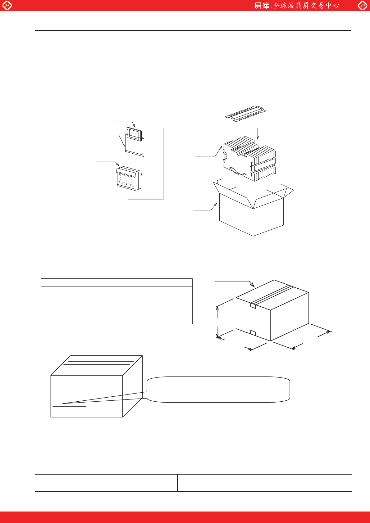
8. Packaging
8.1 Carton (internal package)
(1) Packaging Form
Corrugated cardboard box and polyethylene foam as shock absorber
(2) Packaging Method
Static electricity
㽲
protective sack
Corrugated
Cardboard
1)2)
TFT LCD(1p)
www.panelook.com
G050032-C971
Holder
㽳
(Corrugated
cardboard)
Sheet 28
Note 1): Total weight : (Approx.) 10kg
Note 2): Acceptable number of carton piling: 3 sets
Acceptable number of palette piling: 2 sets
(3) Packaging Material
Number Quantity Description
c
d
e
f
25p
1set
1p
1p
-
Static electricity
Protective sack
Holder
Carton
Plastics adhesive tape
(4) Carton Marking
Toshiba Matsushita Display Technology Co,. Ltd.
MADE IN XXXXXX
㽴
Carton
Plastics
㽵
adhesive tape
301 mm
354 mm
454 mm
Toshiba Matsushita Display Technology Co.,Ltd
Date:2004-11-04 New No.NR-LTD121EC5V-11
Date: - - Old No.
m# Special m Addition m Change
One step solution for LCD / PDP / OLED panel application: Datasheet, inventory and accessory!
www.panelook.com
Page 30
Global LCD Panel Exchange Center
Specification No.
9. Warranty
Warranty clause will be decided separately.
10. Regulation
The set (which our LCD module is assembled into) to conform the regulations below, take measures in set side. Toshiba
Matsushita Display Technology is not liable for the regulations to the complete set, nor can guarantee our LCD module
conform the regulation by itself.
a) Examples of EMI Regulations
FCC : PART15 CLASS B
VCCI : CLASS B
CISPR : CLASS B
b) Examples of Safety Regulations
IEC 60950
UL 60950
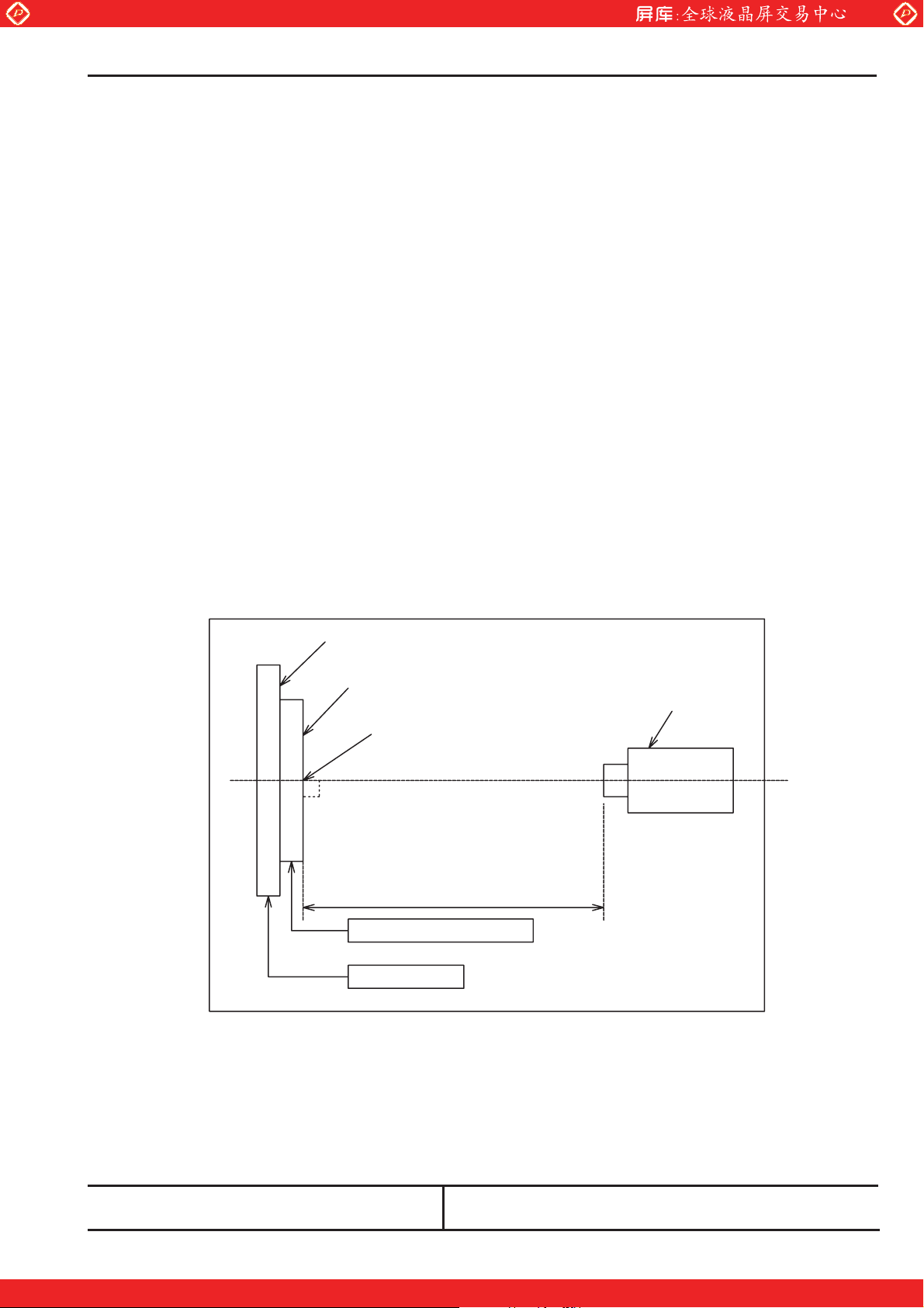
11. Measuring Method
11.1 Measuring System
www.panelook.com
G050032-C971
Sheet 29
㪯䍎㪰 㫊 㫋 㪸 㪾 㪼
LCD Module bilt in Backlight
Photmeter
Screen Center
500 mm
LCD Module Driving Circuit
Stage Controller
Light Shielded Room
(1) The measurement point is the center of the active area except for the measurement of Luminance Uniformity.
(2) Photometer : BM-5A / BM-7 TOPCON (Aperture 2q )
Toshiba Matsushita Display Technology Co.,Ltd
Date:2004-11-04 New No.NR-LTD121EC5V-11
Date: - - Old No.
m# Special m Addition m Change
One step solution for LCD / PDP / OLED panel application: Datasheet, inventory and accessory!
www.panelook.com
Page 31
Global LCD Panel Exchange Center
Specification No.
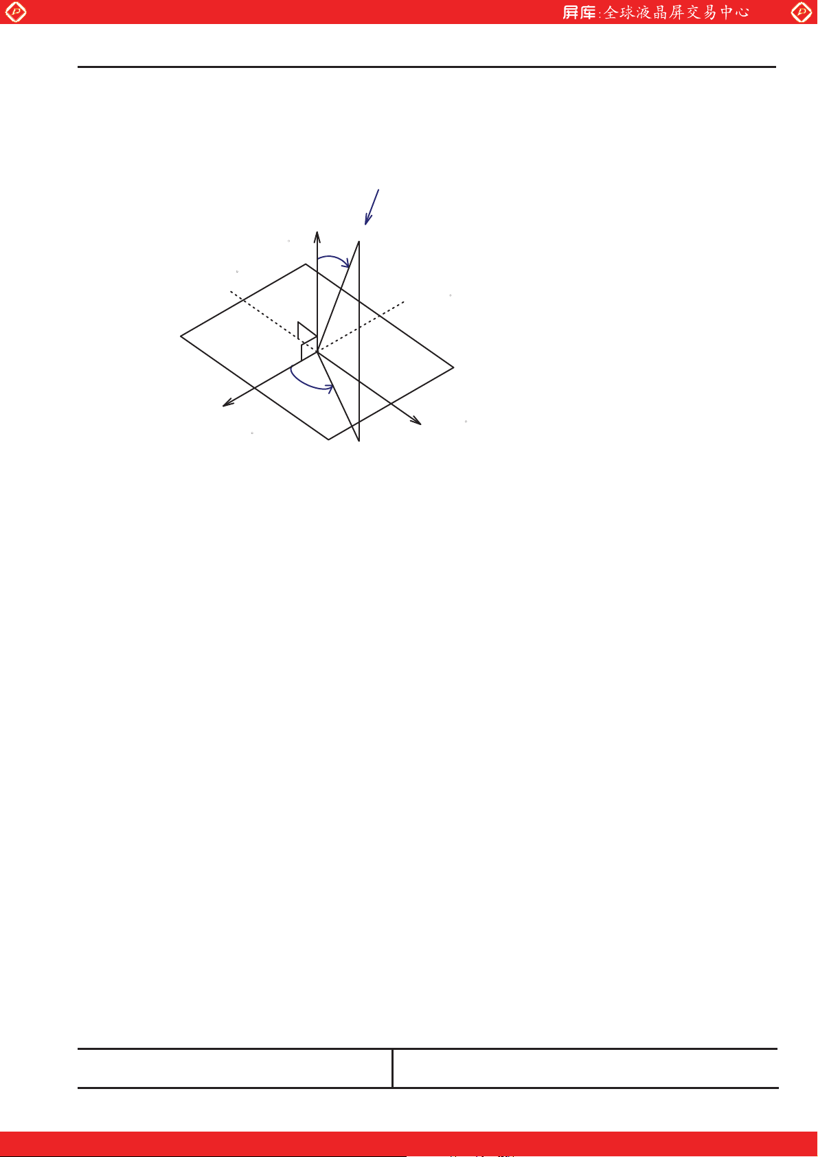
(3) Definition of I and T :
www.panelook.com
Measurement
Direction
Z
G050032-C971
Sheet 30
Left
Side
I
( =-90 )
X
Lower
I
(=0)
Side
(=0)
T
I
T
Upper
Side
I
( =180 )
Right
Side
I
( =90 )
Y
11.2 Measuring Methods
(1) Luminance:
The luminance of the center on a white raster (gray scale level L63) shall be measured.
Measurement shall be executed 30 minutes after the lamp is lit up.
(2) Contrast Ratio:
The contrast ratio can be calculated by the following expression.
Contrast Ratio (CR) = L63 / L0
L63 : Luminance on the white raster (gray scale level L63)
L 0 : Luminance on the black raster (gray scale level L0)
(3) Viewing Angle
Viewing angle is defined as the angles(
(Refer to 11.1(3) for the axes.)
T, I
), in which specified contrast ratio can be obtained.
Toshiba Matsushita Display Technology Co.,Ltd
Date:2004-11-04 New No.NR-LTD121EC5V-11
Date: - - Old No.
m# Special m Addition m Change
One step solution for LCD / PDP / OLED panel application: Datasheet, inventory and accessory!
www.panelook.com
Page 32
Global LCD Panel Exchange Center
Specification No.
(4) Luminance Uniformity:
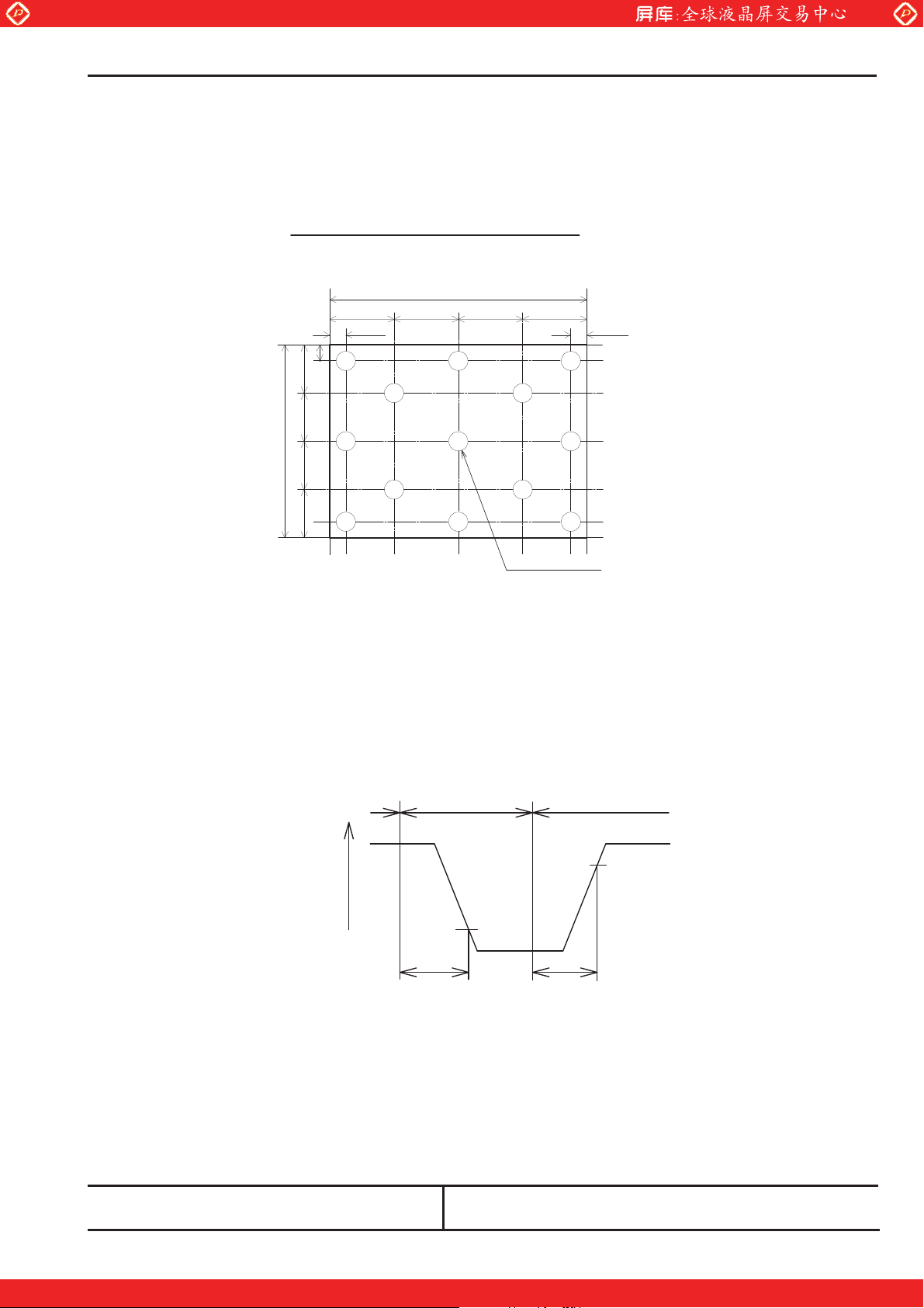
The Luminance should be measured at 13 positions on white raster(gray scale level L63).
Uniformity can be calculated by the following expression.
Maximum Luminance
Luminance Uniformity = u 100%
Minimum Luminance
10 mm
www.panelook.com
Horizontal Line
W
10 mm
G050032-C971
W/4W/4W/4 W/4
10 mm
Sheet 31
(5) Chromaticity :
The values(x,y) of chromaticity coordinates should be measured for the White, Red, Green and Blue Raster(gray scale
level L63) each with a photometer.
(6) Response Time :
The response time (t
pixels.
Input Signal:
1
W/4W/4W/4W/4
54
W
9
Vertical Line Number [Pixel]
ON
, t
OFF
11 12 13
) is measured with a photo detector (photodiode) which measures the light intensity of the
All LowAll High
(White Display)
10
32
876
Display Center
All High
(White Display)(Black Display)
Light
Intensity
90%
10%
t
ON
: Turn on time is the time for a photo detector output waveform to go from maximum value to 10% of its maximum.
t
ON
t
: Turn off time is the time for a photo detector output waveform to go from zero to 90% of its maximum.
OFF
Photodiode : S1223-01 HAMAMATSU PHOTONICS K.K.
White Display : White Raster (gray scale level L63)
Black Display : Black Raster (gray scale level L0)
Toshiba Matsushita Display Technology Co.,Ltd
Date:2004-11-04 New No.NR-LTD121EC5V-11
Date: - - Old No.
t
OFF
m# Special m Addition m Change
One step solution for LCD / PDP / OLED panel application: Datasheet, inventory and accessory!
www.panelook.com
Page 33
Global LCD Panel Exchange Center
Specification No.
12. EDID
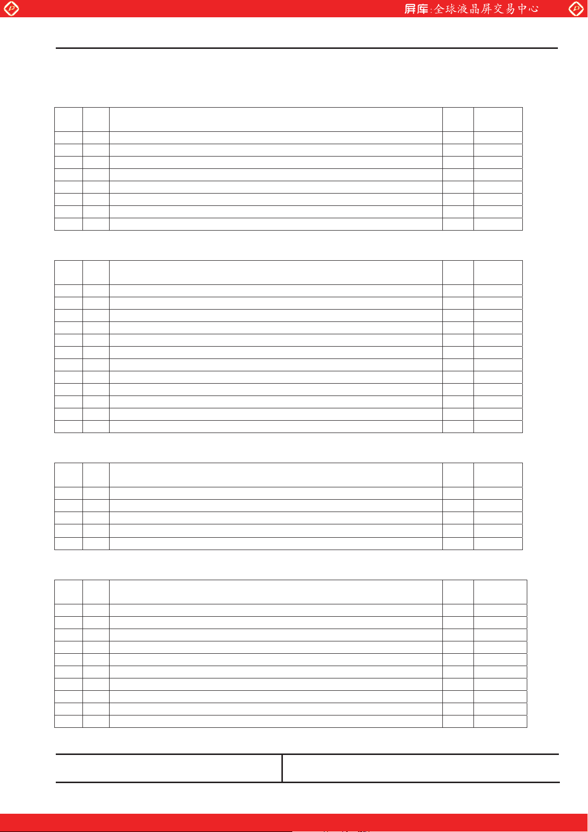
This is the EDID data format to support displays as defined in the VESA Plug & Display.
Header
Byte
Byte
(dec)
(hex)
0 00 Header 00 00000000
1 01 Header FF 11111111
2 02 Header FF 11111111
3 03 Header FF 11111111
4 04 Header FF 11111111
5 05 Header FF 11111111
6 06 Header FF 11111111
7 07 Header 00 00000000
Vendor / Product ID / EDID Version
Byte
Byte
(dec)
(hex)
8 08 EISA manufacture code = 3 Character ID 30 00110000
9 09 EISA manufacture code (Compressed ASCII) 64 01100100
10 0A Panel Supplier Reserved – Product Code 50 01010000
11 0B Panel Supplier Reserved – Product Code 53 01010011
12 0C LCD module Serial No - Preferred but Optional (“0” if not used) 01 00000001
13 0D LCD module Serial No - Preferred but Optional (“0” if not used) 01 00000001
14 0E LCD module Serial No - Preferred but Optional (“0” if not used) 01 00000001
15 0F LCD module Serial No - Preferred but Optional (“0” if not used) 01 00000001
16 10 Week of manufacture Value
17 11 Year of manufacture Value
18 12 EDID structure version # = 01 00000001
19 13 EDID revision # = 02 00000010
Display Parameters
Byte
Byte
(dec)
(hex)
20 14 Video I/P definition = Digital I/P (80h) 80 10000000
21 15 Max H image size = (Rounded to cm) 19 00011101
22 16 Max V image size = (Rounded to cm) 12 00010101
23 17
24 18 Feature support ( no DPMS, Active off, RGB, timing BLK 1) 0A 00001010
Display gamma = (gamma ×100)-100 = Example: ( 2.2100 ) – 100 = 120
Panel Color Coordinates
Byte
Byte
(dec)
(hex)
25 19 Red/Green Low bit (RxRy/GxGy) 80 10000000
26 1A Blue/White Low bit (BxBy/WxWy) 85 10000101
27 1B Red X 97 10010111
28 1C Red Y 58 01011000
29 1D Green X 4F 01001111
30 1E Green Y 87 10000111
31 1F Blue X 26 00100110
32 20 Blue Y 1F 00011111
33 21 White X 50 01010000
34 22 White Y 54 01010100
www.panelook.com
G050032-C971
Field Name and Comments
Field Name and Comments
Field Name and Comments
Field Name and Comments
Sheet 32
Value
(hex)
Value
(hex)
Value
(hex)
96 10010110
Value
(hex)
Value
(binary)
Value
(binary)
Value
(binary)
Value
(binary)
Toshiba Matsushita Display Technology Co.,Ltd
Date:2004-11-04 New No.NR-LTD121EC5V-11
Date: - - Old No.
m# Special m Addition m Change
One step solution for LCD / PDP / OLED panel application: Datasheet, inventory and accessory!
www.panelook.com
Page 34
Global LCD Panel Exchange Center
Specification No.
Established Timings
Byte
Byte
(dec)
(hex)
35 23 Established timings 1 (00h if not used) 00 00000000
36 24 Established timings 2 (00h if not used) 00 00000000
37 25 Manufacturer’s timings (00h if not used) 00 00000000
Standard Timing ID
Byte
Byte
(dec)
(hex)
38 26 Standard timing ID1 (01h if not used) 61 01100001
39 27 Standard timing ID1 (01h if not used) 40 01000000
40 28 Standard timing ID2 (01h if not used) 01 00000001
41 29 Standard timing ID2 (01h if not used) 01 00000001
42 2A Standard timing ID3 (01h if not used) 01 00000001
43 2B Standard timing ID3 (01h if not used) 01 00000001
44 2C Standard timing ID4 (01h if not used) 01 00000001
45 2D Standard timing ID4 (01h if not used) 01 00000001
46 2E Standard timing ID5 (01h if not used) 01 00000001
47 2F Standard timing ID5 (01h if not used) 01 00000001
48 30 Standard timing ID6 (01h if not used) 01 00000001
49 31 Standard timing ID6 (01h if not used) 01 00000001
50 32 Standard timing ID7 (01h if not used) 01 00000001
51 33 Standard timing ID7 (01h if not used) 01 00000001
52 34 Standard timing ID8 (01h if not used) 01 00000001
53 35 Standard timing ID8 (01h if not used) 01 00000001
Timing Descriptor #1
Byte
Byte
(dec)
(hex)
54 36 Pixel Clock/10,000 (LSB) 64 01100100
55 37 Pixel Clock/10,000 (MSB) 19 00011001
56 38 Horizontal Active = xxxx pixels (lower 8 bits) Note 00 00000000
57 39 Horizontal Blanking (Thbp) = xxxx pixels (lower 8 bits) 40 01000000
58 3A Horizontal Active/Horizontal blanking (Thbp) (upper4:4 bits) 41 01000001
59 3B Vertical Active = xxxx lines 00 00000000
60 3C Vertical Blanking (Tvbp) = xxxx lines (DE Blanking min for DE only panels) 26 00100110
61 3D Vertical Active : Vertical Blanking (Tvbp) (upper4:4 bits) 30 00110000
62 3E Horizontal Sync, Offset (Thfp) = xxxx pixels 18 00011000
63 3F Horizontal Sync, Pulse Width = xxxx pixels 88 10001000
64 40 Vertical Sync, Offset (Tvfp) = xx lines Sync Width = xx lines 36 00110110
65 41 Horizontal Vertical Sync Offset/Width upper 2 bits 00 00000000
66 42 Horizontal Image Size =xxx mm F6 00011111
67 43 Vertical image Size = xxx mm B9 11010111
68 44 Horizontal Image Size / Vertical image size 00 00000000
69 45 Horizontal Border = 0 (Zero for Notebook LCD) 00 00000000
70 46 Vertical Border = 0 (Zero for Notebook LCD) 00 00000000
71 47 EDID Standard 18 00011000
www.panelook.com
G050032-C971
Field Name and Comments
Field Name and Comments
Field Name and Comments
Sheet 33
Value
(hex)
Value
(hex)
Value
(hex)
Value
(binary)
Value
(binary)
Value
(binary)
Toshiba Matsushita Display Technology Co.,Ltd
Date:2004-11-04 New No.NR-LTD121EC5V-11
Date: - - Old No.
m# Special m Addition m Change
One step solution for LCD / PDP / OLED panel application: Datasheet, inventory and accessory!
www.panelook.com
Page 35
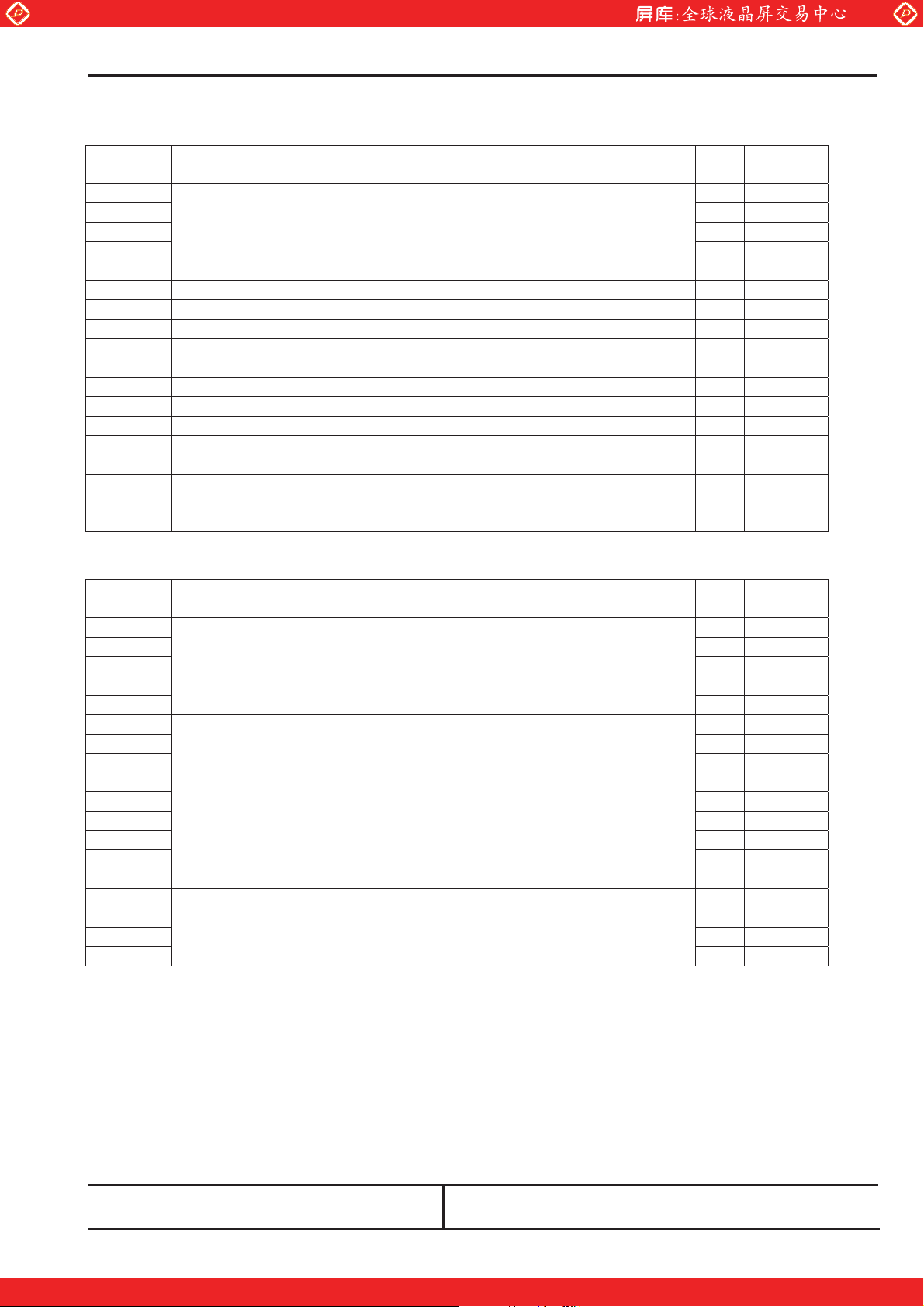
Global LCD Panel Exchange Center
Specification No.
Timing Descriptor #2 Manufacturer’s Specified Range Timing Descriptor
Byte
Byte
(dec)
(hex)
72 48 Header : 00 00 00 0F 00 00 00000000
73 49 00 00000000
74 4A 00 00000000
75 4B 0F 00001111
76 4C 00 00000000
77 4D Value = HSPW
78 4E Value = HSPW
79 4F Value = Thbp
80 50 Value = Thbp
81 51 Value = VSPW
82 52 Value = VSPW
83 53 Value = Tvbp
84 54 Value = Tvbp
85 55 Thp
86 56 Thp
87 57 Tvp
88 58 Tvp
= value*2 + HA
min
= value*2 + HA
max
= value*2 + VA
min
= value*2 + VA
max
/2 (pixel clks) 06 00000110
min
/2 (pixel clks 42 01000010
max
/2 (pixel clks) 02 00000010
min
/2 (pixel clks) 44 01000100
max
/2 (line pulses) 01 00000001
min
/2 (line pulses) 03 00000011
max
/2 (line pulses 04 00000100
min
/2 (line pulses 07 00000111
max
89 59 Module “A” Revision = Example: 00, 01, 02, 03, etc. 00 00000000
Timing Descriptor #3
Byte
Byte
(dec)
(hex)
90 5A Model No. 00 00000000
91 5B Header : 00 00 00 FE 00 00 00000000
92 5C 00 00000000
93 5 D Termin a t o r : 0A B l a n k : 20 FE 11111110
94 5E 00 00000000
95 5F T 54 01010100
96 60 M 4D 01001101
97 61 D 44 01000100
98 62 I 49 01001001
99 63 S 53 01010011
100 64 P 50 01010000
101 65 L 4C 01001100
102 66 A 41 01000001
103 67 Y 59 01011001
104 68 Terminator : 0A 0A 00001010
105 69 Blank : 20 20 00100000
106 6A 20 00100000
107 6B 20 00100000
www.panelook.com
G050032-C971
Field Name and Comments
pixel clks
pixel clks
lines
lines
Field Name and Comments
(pixel clks) Note 22 00100010
(pixel clks) Note 24 00100100
(line pulses) 03 00000011
(line pulses) 08 00001000
Sheet 34
Value
(hex)
Value
(hex)
Value
(binary)
Value
(binary)
Toshiba Matsushita Display Technology Co.,Ltd
Date:2004-11-04 New No.NR-LTD121EC5V-11
Date: - - Old No.
m# Special m Addition m Change
One step solution for LCD / PDP / OLED panel application: Datasheet, inventory and accessory!
www.panelook.com
Page 36
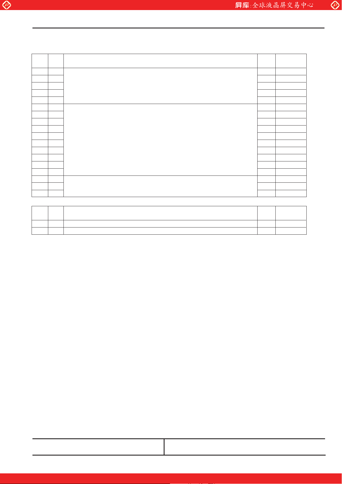
Global LCD Panel Exchange Center
Specification No.
Timing Descriptor #4
Byte
Byte
(dec)
(hex)
108 6C Module Serial 00 00000000
109 6D 00 00000000
110 6E Header : 00 00 00 FE 00 00 00000000
111 6F Terminator : 0A FE 11111110
112 70 Blank : 20 00 00000000
113 71 L Product Name: 4C 01001100
114 72 T 54 01010100
115 73 D 44 01000100
116 74 1 31 00110001
117 75 2 32 00110010
118 76 1 31 00110001
119 77 E 45 01000101
120 78 C 43 01000011
121 79 5 35 00110111
122 7A V 56 01010110
123 7B Terminator : 0A 0A 00001010
124 7C Blank : 20 20 00100000
125 7D 20 00100000
Byte
Byte
(dec)
(hex)
126 7E Extension flag (# of optional 128 EDID extension blocks to follow, Typ = 0) 00 00000000
127 7F Checksum (The 1-byte sum of all 128 bytes in this EDID block shall = 0) - -
www.panelook.com
G050032-C971
Field Name and Comments
Field Name and Comments
Sheet 35
Value
(hex)
Value
(hex)
Value
(binary)
Value
(binary)
Toshiba Matsushita Display Technology Co.,Ltd
Date:2004-11-04 New No.NR-LTD121EC5V-11
Date: - - Old No.
m# Special m Addition m Change
One step solution for LCD / PDP / OLED panel application: Datasheet, inventory and accessory!
www.panelook.com
 Loading...