

Page 1
Toshiba Matsushita Display Technology Co., Ltd
PRODUCT INFORMATION
14cm COLOUR TFT-LCD MODULE
(5.7 TYPE)
LTA057A340F
(a-Si TFT)
All information is subject to change without notice. Please read bottom notes.
FEATURES:
(1)5.7” QVGA color display
(2)Wide Viewing Angle (Vertical: 120 degrees, Horizontal: 140 degrees)
(3)LED B/L [ 18pcs. (6pcs. x 3rows)]
(4)Replaceable structure of LED unit
(5)RoHS compatible
TENTATIVE
RoHS compatible
MECHANICAL SPECIFICATIONS
Item Specifications
Dimensional Outline (typ.) 144.0 (W) x 104.6 (H) x 8.3 max.(D) mm
Number of Pixels 320 (W) x 240 (H) pixels
Active Area 115.2 (W) x 86.4 (H) mm
Pixel Pitch 0.36 (W) x 0.36 (H)
Weight (approximately) 125 g
Backlight Sidelight (LEDs)
ABSOLUTE MAXIMUM RATINGS
Item Min. Max. Unit
Supply Voltage
(VDD) -0.3 4.0 V
(V
) 0 30.0 V
LED
Input Signal Voltage (VIN) -0.3 VDD+0.3 V
Operating Temperature *1 -20 70 °C
Storage Temperature -30 80 °C
Storage Humidity
(Max. wet bulb temperature = 39°C)
*1: Only operation is guarantied at Operating Temperature. Display quality is evaluated at +25°C.
10 90 %(RH)
ELECTRICAL SPECIFICATION (Ta=25°C) (RECOMMENDED OPERATION CONDITION)
Item Min. Typ. Max. Unit Remarks
Supply Voltage
(VDD)
)*2 --- 19.2 --- V I
(V
LED
3.0 3.3 3.6 V
=15.0mA,
LED
High Level Input Voltage (VIH) 0.8 VDD --- VDD V
Low Level Input Voltage (VIL) 0 --- 0.2 VDD V
Current Consumption
Power Consumption
*2: between V
LED1+
- V
*3*4
*3 *4
--- 1.36 --- W I
LED1-
(IDD) --- 150 --- mA
(I
) --- 15.0 25.0 mA
LED
or V
LED2+
- V
LED2-
or V
LED3+
- V
*3: 8 color bars pattern *4: Except the efficiency of LED driver
LED3-
=15.0mA
LED
OPTICAL SPECIFICATION (Ta=25°C)
Item Min. Typ. Max. Unit Remarks
Contrast Ratio (CR) 250 500 --- ---
(Upper+Lower) --- 120 --- degrees Viewing Angle
(CR ≥ 10)
Response Time
Luminance (L) 320 400 --- cd/m2 I
LED Life Time (MTBF)
*5: Conditions;Ta=25°C, continuous lighting
*6: Definitions of failure; 1) Lcd luminance becomes half of the minimum value. 2) LED doesn’t light normally .
(Left+Right) --- 140 --- degrees
(TON) --- 15 50 ms
(T
) --- 25 50 ms
OFF
*5 *6
20,000 h I
=15.0mA
LED
=15.0mA
LED
*The information contained herein is presented only as a guide for the applications of our products. No responsibility is assumed by
Toshiba Matsushita Display Technology or other rights of the third parties which may result from its use. No license is granted by
implication or otherwise under any patent or patent rights of Toshiba Matsushita Display Technology or others.
*The information contained herein may be changed without prior notice. It is therefore advisable to contact Toshiba Matsushita Display
Technology before proceeding with the design of equipment incorporating this product.
(1/9) 2007-08-01 (Ver.1.4R)
Page 2

DIMENSIONAL OUTLINE
<Front side>
8.3 MAX.
2.0
(10.4)
(12.3)
TENTATIVE
104.6
90.2(Bezel Opening)
86.4(Active Area)
Unit : mm
Standard tolerance : ±0.5
4.0
5.9+/-0.8
(12.5)
(14.4)
LTA057A340F
8.3 MAX.
4.5
8.3 MAX.
4-diameter 1.6
depth max 3.1
4-R0.3 4-R0.3
1.5
89.4 7.6
6.2
Main viewing
angle direction
2.5
115.2(Active Area)
119(Bezel Opening)
12.5
14.4+/-0.8
144
7.0
8.0
4-diameter 5.0
4-hole depth max 3.1
1.2
4.0
1.2 1.5
4.0
60.6
22.0
(2/9) 2007-08-01 (Ver.1.4R)
Page 3
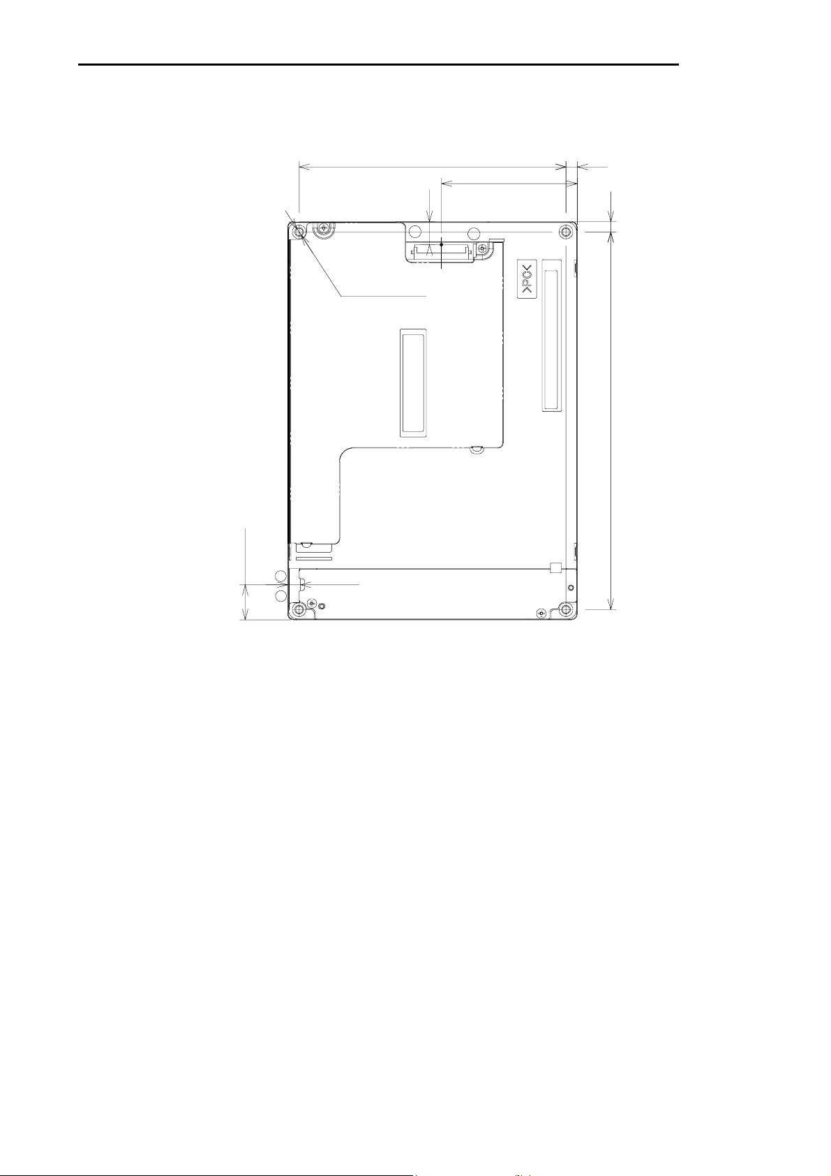
<Rear side>
4-diameter 2.6
depth max. 4.2
96.4 4.1
49.1+/-1
8.3
CN1
33
1
LTA057A340F
136.6 3.7
12.7+/-1
CN2
6
4.5+/-1
1
(3/9) 2007-08-01 (Ver.1.4R)
Page 4

BLOCK DIAGRAM
DC/DC
Converter
CN1
I/F Connector
Gray Scale
Manipulation
Voltage
Generation
Circuit
Panel
Controller
1,1
1,2
Y-Driver IC
320 pixels
X,1
X,2
1,Y
X,Y
X,2401,240
SEQUENCE OF POWER SUPPLIES AND SIGNALS
LED LED
LED
LCD Panel
320 x 240 pixels
X-Driver IC
320,1
320,2
320,Y
320,240
240 pixels
LTA057A340F
Connector
CN2
10ms(max.)
0.5m s(min. )
V
DD
CLK
DE
DATA
H,V-sync
U/D,L/R
LED B/L
OFF
3.0V
0.2V
0.2V
DD DD
250m s(min. )
40ms (max.)
0ms(m in.)
ON
100m s(max. )
0.1m s(min. )
3.0V
40ms(m ax.)
0ms(m in.)
0.2V
(4/9) 2007-08-01 (Ver.1.4R)
500ms(min.)
0.2V
0ms( min.)
0.2V
Page 5

TIMING CHART
Vsync
Hsync
DE
RGB Data
tvd
239
240
tvfp
tvw
tvblnk
tvds
th
1
tv
tvd
2
X-1
LTA057A340F
X+1
X
X+2
thw
th
Hsync
thfp
DE
RGB Data
thds
1
2345
tep
thde
320
NCLK
TIMING SPECIFICA TION
Item Symbol Min. Typ. Max. Unit
Frame Period tv
Vertical Display Term tvd 240 240 240 clk
Vertical Blanking Term tvblnk 20 45 70 th
V-sync Pulse Width tvw 1.0 - 34 th
Vertical Front Porch tvfp - - - th
251 262 340 th
15.81 16.67 17.81 ms
Vertical Data Starting Position tvds 7.0 7.0 7.0 th
Horizontal Period th
360 400 450 tc
49.03 63.6 70.96 us
Horizontal Display Term thde 320 320 320 tc
H-sync Pulse Width thw 2 96 - tc
Horizontal Front Porch thfp - - - tc
Horizontal Data Sync Period thds 11 - - tc
Clock Period tc 6.0 6.30 8.89 MHz
Clock "H" Time tch - - - ns
Clock "L" Time tcl - - - ns
Duty Rate
tch/tc
35.0 50.0 65.0 %
Set Up Time tds 5.0 - - ns
Hold Time tdh 10.0 - - ns
DE Pulse Width tep 2 320 th-10 tc
(5/9) 2007-08-01 (Ver.1.4R)
Page 6

LTA057A340F
CONNECTOR PIN ASSIGNMENT FOR INTERFACE
CN1 INPUT SIGNAL
Connector: IMSA-9637S-33A-GF / IRISO electronics co., LTD.
0.5mm pitch, lower face contacting (gilding)
Terminal No. Symbol Function
10 R42) Red Display Data
12 GND1)
13 G02) Green Display Data (LSB)
14 G12) Green Display Data
15 G22) Green Display Data
16 G32) Green Display Data
17 G42) Green Display Data
18 G52) Green Display Data (MSB)
19 GND1)
20 B02) Blue Display Data (LSB)
21 B12) Blue Display Data
22 B22) Blue Display Data
23 B32) Blue Display Data
24 B42) Blue Display Data
25 B52) Blue Display Data (MSB)
26 GND1)
27 DE Data Enable
28 VDD 3.3V
29 VDD 3.3V
30 R/L Horizontal Reverse(“L” level or Open : Normal, ”H “ level : Reverse)
31 U/D Vertical Reverse(“H” level : Normal, “L” level or Open : Reverse)
32 GND1)
33 NC3) Non Connection
Note 1) Please connect GND pin to ground. Don’t use it as no-connect nor connection with high impedance.
Note 2) Refer to 8 pages.
Note 3) NC terminal should be open. (Don’t use.)
CN2 LED POWER SOURCE
Connector: SM06B-SHLS-TF(LF)(SN) / JAPAN SOLDERLESS TERMINAL MFG CO., LTD.
Mating Connector: SHLP-06V-S-B (housing), SSHL-003T-P02 (contact pin)
Terminal No. Symbol Function
1 GND1)
2 CLK Clock
3 H-sync Horizontal Sync
4 V-sync Vertical Sync
5 GND1)
6 R02) Red Display Data (LSB)
7 R12) Red Display Data
8 R22) Red Display Data
9 R32) Red Display Data
11 R52) Red Display Data (MSB)
/ JAPAN SOLDERLESS TERMINAL MFG CO., LTD.
1 V
2 V
3 V
4 V
5 V
6 V
LED1 POWER SUPPLY(Cathode)
LED1-
LED1 POWER SUPPLY(Anode)
LED1+
LED2 POWER SUPPLY(Cathode)
LED2-
LED2 POWER SUPPLY(Anode)
LED2+
LED3 POWER SUPPLY(Cathode)
LED3-
LED3 POWER SUPPLY(Anode)
LED3+
(6/9) 2007-08-01 (Ver.1.4R)
Page 7

EQUIVALENT CIRCUIT OF LED
Terminal No.1
No.2
No.3
No.4
Connector (CN2)
No.5
No.6
LTA057A340F
(7/9) 2007-08-01 (Ver.1.4R)
Page 8

256k (k=1024) COLORS COMBINATION TABLE
Basic
Color
Gray
Scale of
Red
Gray
Scale of
Green
Gray
Scale of
Blue
Gray
Scale of
White &
Black
Display R5 R4 R3 R2 R1 R0 G5 G4 G3 G2 G1 G0 B5 B4 B3 B2 B1 B0
Black L L L L L L L L L L L L L L L L L L ---
Blue L L L L L L L L L L L L H H H H H H ---
Green L L L L L L H H H H H H L L L L L L ---
Light Blue L L L L L L H H H H H H H H H H H H ---
Red H H H H H H L L L L L L L L L L L L --Purple H H H H H H L L L L L L H H H H H H --Yellow H H H H H H H H H H H H L L L L L L ---
White H H H H H H H H H H H H H H H H H H ---
Black L L L L L L L L L L L L L L L L L L L 0
L L L L L H L L L L L L L L L L L L L 1
Dark
↑
↓
Light
Red H H H H H H L L L L L L L L L L L L Red L63
Black L L L L L L L L L L L L L L L L L L L 0
Dark
↑
↓
Light
Green L L L L L L H H H H H H L L L L L L Green L63
Black L L L L L L L L L L L L L L L L L L L 0
Dark
↑
↓
Light
Blue L L L L L L L L L L L L H H H H H H Blue L63
Black L L L L L L L L L L L L L L L L L L L 0
Dark
↑
↓
Light
White H H H H H H H H H H H H H H H H H H White L63
L L L L H L L L L L L L L L L L L L L 2
:
:
H H H H L H L L L L L L L L L L L L L61
H H H H H L L L L L L L L L L L L L L62
L L L L L L L L L L L H L L L L L L L 1
L L L L L L L L L L H L L L L L L L L 2
:
:
L L L L L L H H H H L H L L L L L L L61
L L L L L L H H H H H L L L L L L L L62
L L L L L L L L L L L L L L L L L H L 1
L L L L L L L L L L L L L L L L H L L 2
:
:
L L L L L L L L L L L L H H H H L H L61
L L L L L L L L L L L L H H H H H L L62
L L L L L H L L L L L H L L L L L H L 1
L L L L H L L L L L H L L L L L H L L 2
:
:
H H H H L H H H H H L H H H H H L H L61
H H H H H L H H H H H L H H H H H L L62
LTA057A340F
Gray Scale
Level
:
:
:
:
:
:
:
:
:
:
:
:
:
:
:
:
L3…
L60
L3…
L60
L3…
L60
L3…
L60
(8/9) 2007-08-01 (Ver.1.4R)
Page 9

LTA057A340F
!
FOR SAFETY
LCD module is generally designed with precise part s to achieve light weighted thin mechanical dimensions.
In using our Modules, make certain that you fully understand and put into practice the warnings and safety precautions detailed
in Engineering Information No.EE-N001,"CAUTIONS AND INSTRUCTIONS FOR TOSHIBA LCD MODULES".
Refer to individual specifications and TECHNICAL DATA sheets (hereinafter called "TD") for more detailed technical
information.
1) SPECIAL PURPOSES
A) Toshiba Matsushita Display Technology's Standard LCD Modules have not been customized for operation in extreme
environments or for use in applications where performance failures could be life-threatening or otherwise catastrophic.
B) Since Toshiba Matsushita Display Technology's Standard LCD Modules have not been designed for operation in extreme
environments, they must never be used in devices that will be exposed to abnormally high levels of vibration or shock which
exceed Toshiba Matsushita Display Technology's published specification limits.
C) In addition, since Toshiba Matsushita Display Technology Standard LCD Modules have not been designed for use in
applications where performance failures could be life-threatening or catastrophic, they must never be installed in aircraft
navigation control systems (such as, but not limited to Traffic Collision Avoidance System and Air Traffic Indicator), in military
defense or weapons systems, in critical industrial process-control systems (e.g., those involved in the production of nuclear
energy), or in critical medical device or patient life-support systems.
2) DISASSEMBLING OR MODIFICATION
DO NOT DISASSEMBLE OR MODIFY the module. It may damage sensitive parts inside LCD module, and may cause
scratches or dust on the display.
Toshiba Matsushita Display Technology doses not warrant the module, if customer disassembled or modified it.
3) BREAKAGE OF LCD PANEL
DO NOT INGEST liq uid cryst al material, DO NOT I NHALE this material, and DO NOT CONTACT the material with skin, if LCD
panel is broken and liquid crystal material spills out.
If liquid crystal material comes into mouth or eyes, rinse mouth or eyes out with water immediately.
If this material contact with skin or cloths, wash it off immediately with alcohol and rinse thoroughly with water.
4) GLASS OF LCD PANEL
BE CAREFUL WITH CHIPS OF GLASS that may cause injuring fingers or skin, when the glass is broken.
5) ELECTRIC SHOCK
DISCONNECT POWER SUPPLY before handling LCD module.
DO NOT TOUCH the parts inside LCD module and the fluorescent lamp's connector or cables in order to prevent electric
shock, because high voltage is supplied to these parts from the inverter unit while power supply is turned on.
6) ABSOLUTE MAXIMUM RATINGS AND POWER PROTECTION CIRCUIT
DO NOT EXCEED the absolute maximum rating values under the worst probable conditions caused by the supply voltage
variation, input voltage variation, variation in parts' const ants, environment al temperature, etc., otherwise LCD module may be
damaged.
Employ protection circuit for power supply, whenever the specification or TD specifies it.
Suitable protection circuit should be applied for each system design.
7) RECOMMENDED OPERATION CONDITIONS
The performance and quality of the LCD panel are warranted only when the LCD panel is used within “the recommended
operation conditions”. Toshiba Matsushita Display Technology Co., Ltd. never warrants the performance and quality of the
LCD panel when you use the LCD panel over “the recommended operatio n conditions”, although within “the absolute
maximum rating”.
To use the LCD panel over “the recommended operation conditions” may have bad influence on the characteristics and
reliability of the LCD panel and may shorten the life of the LCD panel.
Therefore, when designing the whole set, not to be over “the recommended operation conditions”, you should fully t ake care of
supply voltage change, characteristic of connection parts, serge of input-and-output line, and surrounding temperature.
8) DISPOSAL
When dispose LCD module, obey to the applicable environmental regulations.
(9/9) 2007-08-01 (Ver.1.4R)
 Loading...