

Toshiba LCD-AD194TW Service Manual
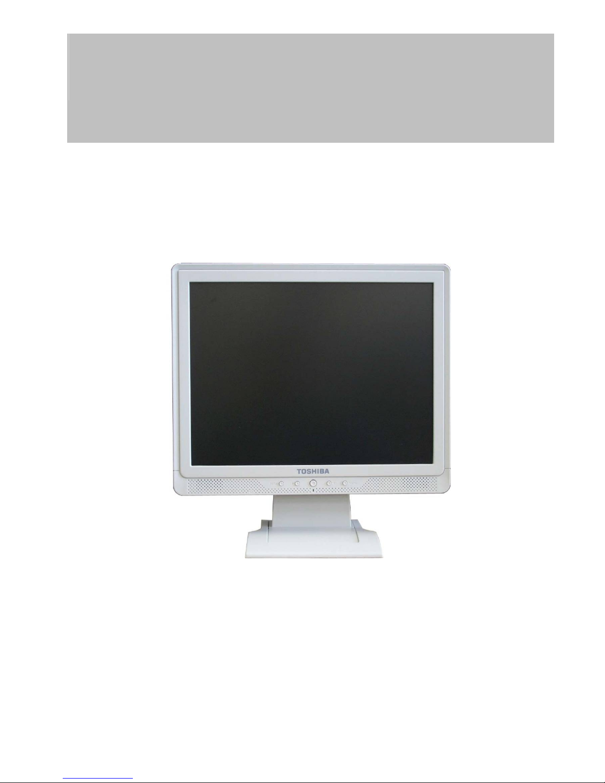
AD194TW TOSHIBA
Page 1 of 62
SERVICE MANUAL
TOSHIBA
LCD-AD194TW
THESE DOCUMENTS ARE FOR REPAIR SERVICE INFORMATION ONLY.EVERY
REASONABLE EFFORT HAS BEEN MADE TO ENSURE THE ACCURACY OF THIS MANUAL;
WE CANNOT GUARANTEE THE ACCURACY OF THIS INFORMATION AFTER THE DATE OF
PUBLICATION AND DISCLAIMS RELIABILITY FOR CHANGES, ERRORS OR OMISSIONS.
MANUFACTURE DATA :Jul-28-2006
AD194TW TOSHIBA
Page 2 of 62
Table of Contents
Table of Contents ----------------------------------------------------------------------------- 02
Revision List ------------------------------------------------------------------------------------04
1. Product Feature ----------------------------------------------------------------------------05
2. LCD Monitor Description -----------------------------------------------------------------05
3. Operation Instructions --------------------------------------------------------------------06
3.1 General Instructions ------------------------------------------------------------------06
3.2 Control Buttons ------------------------------------------------------------------------06
3.3 Adjusting The Picture ----------------------------------------------------------------06
4. Electrical Performance Parameter ------------------------------------------------- 07
4.1 Input Signal Connector --------------------------------------------------------------07
4.2 Factory Preset Display Modes -----------------------------------------------------08
4.3 Power Supply --------------------------------------------------------------------------09
4.3.1 Input/Output Requirements ---------------------------------------------------09
4.3.2 Inverter Max Brightness ------------------------------------------------------- 10
4.3.3 Inverter Min Brightness --------------------------------------------------------10
4.4 Panel Specification ----------------------------------------------------------------11
4.4.1 General Feature (HSD190ME13-A11) -------------------------------------11
4.4.2 Optical Characteristics -------------------------------------------------------12
5. Block Diagram ------------------------------------------------------------------------------13
5.1 Monitor Exploded View -------------------------------------------------------------13
5.2. Disassemble Process --------------------------------------------------------------15
5.3 Software Flow Chart ------------------------------------------------------------------19
5.4. Block Diagram ---------------------------------------------------------------------------21
AD194TW TOSHIBA
Page 3 of 62
5.4.1 Electrical Block Diagram ------------------------------------------------------21
5.4.2 Inverter/Power Board Block Diagram --------------------------------------22
6. Schematic -----------------------------------------------------------------------------------24
6.1 TOP ------------------------------------------------------------------------------------24
6.2 Main Board ---------------------------------------------------------------------------25
6.3 PWPC Board -----------------------------------------------------------------------29
6.4 KeyPad Board -----------------------------------------------------------------------31
6.5 Audio Board ------------------------------------------------------------------------32
7. PCB Layout ---------------------------------------------------------------------------------33
7.1 Main Board ----------------------------------------------------------------------------33
7.2 PWPC Board --------------------------------------------------------------------------35
7.3 Keypad Board -------------------------------------------------------------------------36
7.4 Audio Board ------------------------------------------------------------------------36
8. Maintainability ------------------------------------------------------------------------------36
8.1 Equipments and Tools Requirements -------------------------------------------36
8.2 Trouble Shooting ---------------------------------------------------------------------37
8.2.1 Main Board ---------------------------------------------------------------------37
8.2.2 Key Pad Board ------------------------------------------------------------------39
8.2.3 Power/Inverter Board ------------------------------------------------------40
9. White-Balance, Luminance Adjustment ---------------------------------------------42
10. EDID Content -----------------------------------------------------------------------------44
11. BOM List -----------------------------------------------------------------------------------45
11.1 AD194T——T981KH6NJ4D4ABP ------------------------------------------45~62
AD194TW TOSHIBA
Page 4 of 62
Revision List
Revision Date Change Description
AD194TW TOSHIBA
Page 5 of 62
1. PRODUCT FEATURE
19” a-si TFT Active matrix LCD panel, 0.294mm dot pitch.
Microprocessor controlled scan technology
19 factory presets modes for VGA
?? factory preset modes for DVI
Vertical refresh rate 55Hz to 75 Hz
Horizontal frequency 24kHz to 80kHz
Resolutions: 640 x 350 up to 1280 x 1024
Universal power supply designed for worldwide application
VESA DPMS compliant
VESA DDC2B compliant
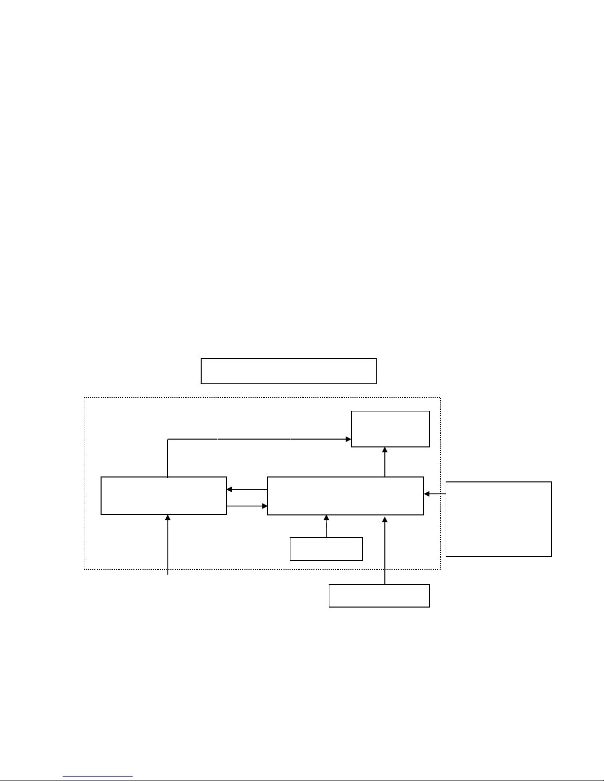
2. LCD MONITOR DESCRIPTION
The LCD Monitor will contain a main board, an inverter/power board, keypad board which house the
flat panel control logic, brightness control logic and DDC.
The power board will provide AC to DC Inverter voltage to drive the backlight of panel and the main
board chips each voltage.
Power board
(
Include: adapter, inverter)
Flat Panel and
CCFL backlight
Main Board
Keyboard
RS232 Connector
For white balance
adjustment in factory
mode
HOST Computer
CCFL Drive.
Video signal, DDC
Monitor Block Diagram
AC IN
100~240V
AD194TW TOSHIBA
Page 6 of 62
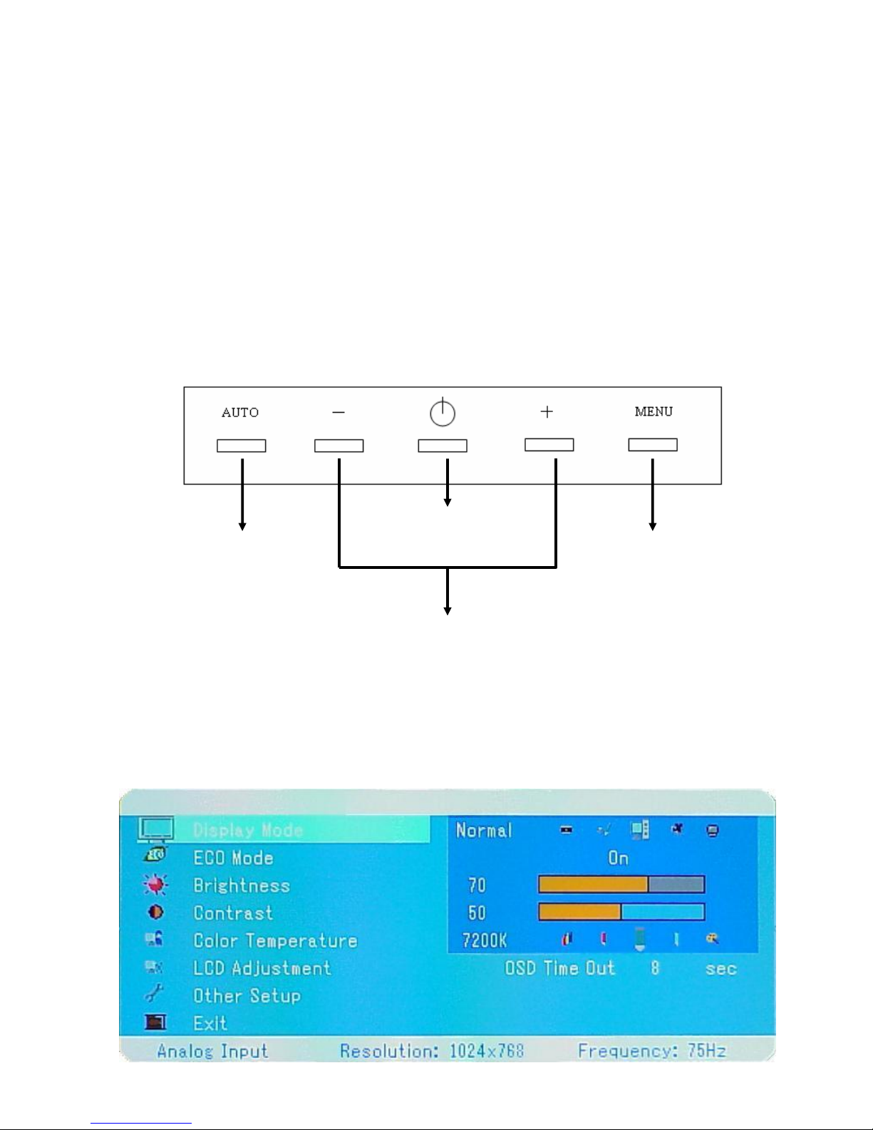
3. OPERATING INSTRUCTIONS
3.1 GENERAL INSTRUCTIONS
Press the power button to turn the monitor on or off. The other control buttons are located
at front panel of the monitor. By changing these settings, the picture can be adjusted to
your personal preferences.
-
The power cord should be connected.
-
Connect the video cable from the monitor to the video card.
-
Press the power button to turn on the monitor, the power indicator will light up.
3.2 CONTROL BUTTONS
3.2.1 KEY CONTROL
3.3 ADJUSTING THE PICTURE
Power On/Off
Auto Adjustment
for Clock, Phase
and H.V. Position
Volume +, - &
Menu Select
OSD Menu
AD194TW TOSHIBA
Page 7 of 62
CONTROL FUNCTION
Display Mode Normal, Text, Cinema, Photo, TV
ECO Mode
Brightness
Contrast sRGB, 6500K, 7200K, 9300K, User
Color temperature
LCD Adjustment
Clock
Phase
H. Position
V. P os iti on
Other Setup
Smooth
OSD H. Position
OSD V. Position
OSD Timeout
OSD Transparency On Off
Mode message On Off
Language Japanese English
Reset
Exit
4. ELECTRICAL PERFORMANCE PARAMETER
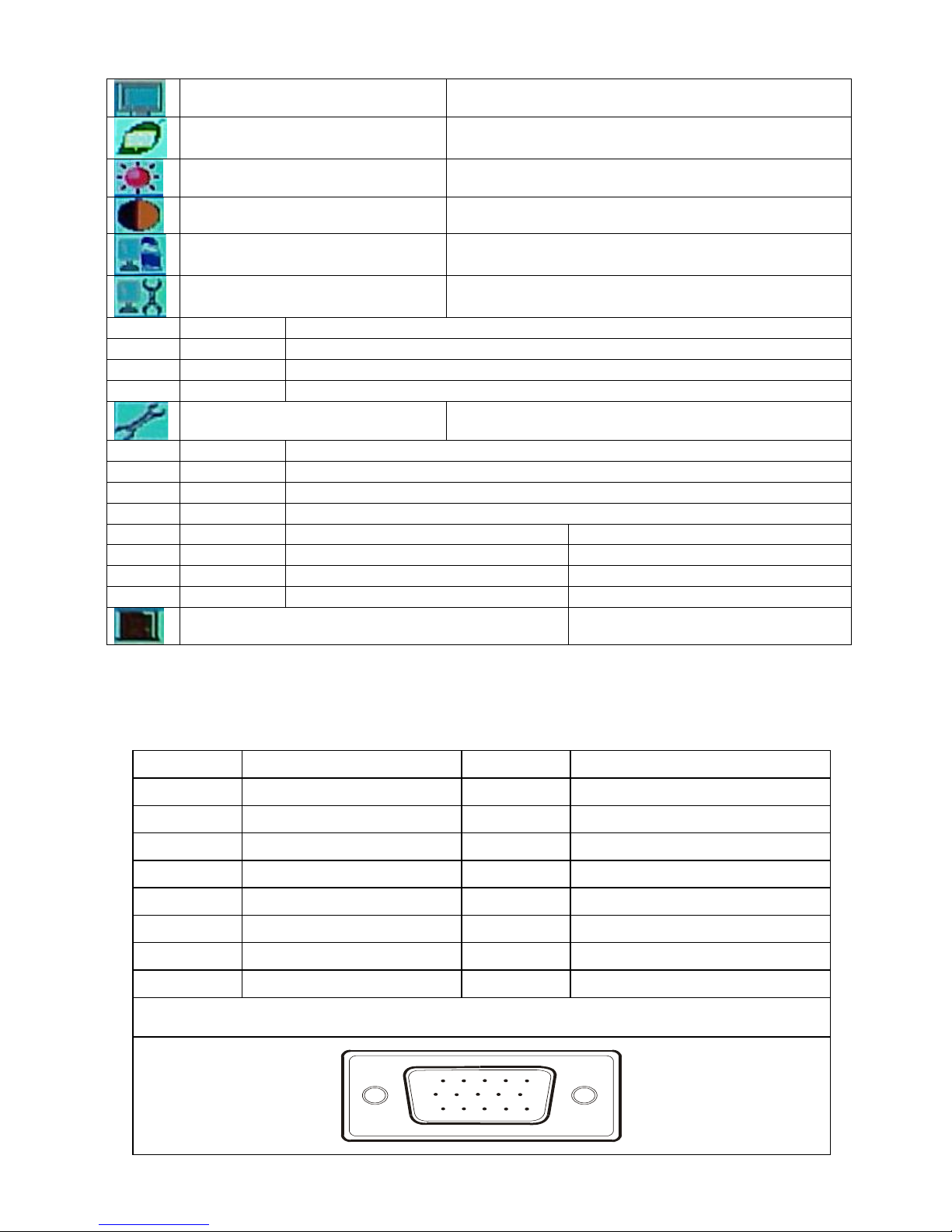
4.1 INPUT SIGNAL CONNECTOR
PIN NO. DESCRIPTION PI N NO. DESCRIPTION
1. Red Video 9. +5V
2. Green Video 10. Detect Cable
3. Blue Video 11. RS232
4. RS232 12. DDC-Serial Data
5. DDC-Return 13. H-Sync
6. R-Ground 14. V-Sync
7. G-Ground 15. DDC-Serial Clock
8. B-Ground
D-SUB 15 PIN CONNECTOR
15
6
10
11 15
AD194TW TOSHIBA
Page 8 of 62
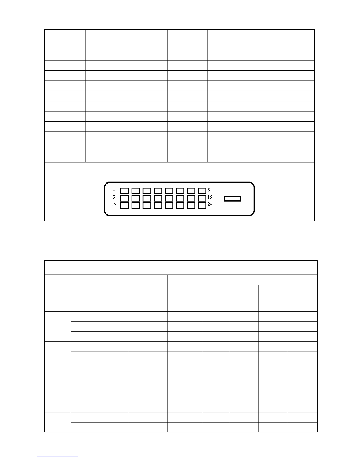
PIN NO. DESCRIPTION PI N NO. DESCRIPTION
1. TMDS data 2 - 13. TMDS data 3 + (NC)
2. TMDS data 2 + 14. + 5V Power
3. TMDS data 2/4 Shield 15. GND(return for +5v,hsync,vsync)
4. TMDS data 4 – (NC) 16. Hot Plug Detect
5. TMDS data 4 + (NC) 17. TMDS data 0 -
6. DDC Clock 18. TMDS data 0 +
7. DDC Data 19. TMDS data 0/5 Shield
8. Analog Vertical Sync 20. TMDS data 5 -
9. TMDS data 1 - 21. TMDS data 5 +
10. TMDS data 1 + 22. TMDS Clock Shield
11. TMDS data 1/3 Shield 23. TMDS Clock +
12. TMDS data3 – (NC) 24. TMDS Clock -
DVI-D 24 PIN CONNECTOR
4.2 FACTORY PRESET DISPLAY MODES:
VESA MODES
Horizontal Vertical
Mode Resolution Total
Nominal
Frequency
+/- 0.5kHz
Sync
Polarity
Nominal
Freq.
+/- 1 Hz
Sync
Polarity
Nominal
Pixel
Clock
(MHz)
640x480@60Hz 800 x 525 31.469 N 59.940 N 25.175
640x480@72Hz 832 x 520 37.861 N 72.809 N 31.500
VGA
640x480@75Hz 840 x 500 37.500 N 75.00 N 31.500
800x600@56Hz 1024 x 625 35.156 N/P 56.250 N/P 36.000
800x600@60Hz 1056 x 628 37.879 P 60.317 P 40.000
800x600@72Hz 1040 x 666 48.077 P 72.188 P 50.000
SVGA
800x600@75Hz 1056x625 46.875 P 75.000 P 49.500
1024x768@60Hz 1344x806 48.363 N 60.004 N 65.000
1024x768@70Hz 1328x806 56.476 N 70.069 N 75.000
XGA
1024x768@75Hz 1312x800 60.023 P 75.029 P 78.750
1280x1024@60Hz 1688x1066 63.981 P 60.020 P 108.000
SXGA
1280x1024@75Hz 1688x1066 79.976 P 75.025 P 135.000
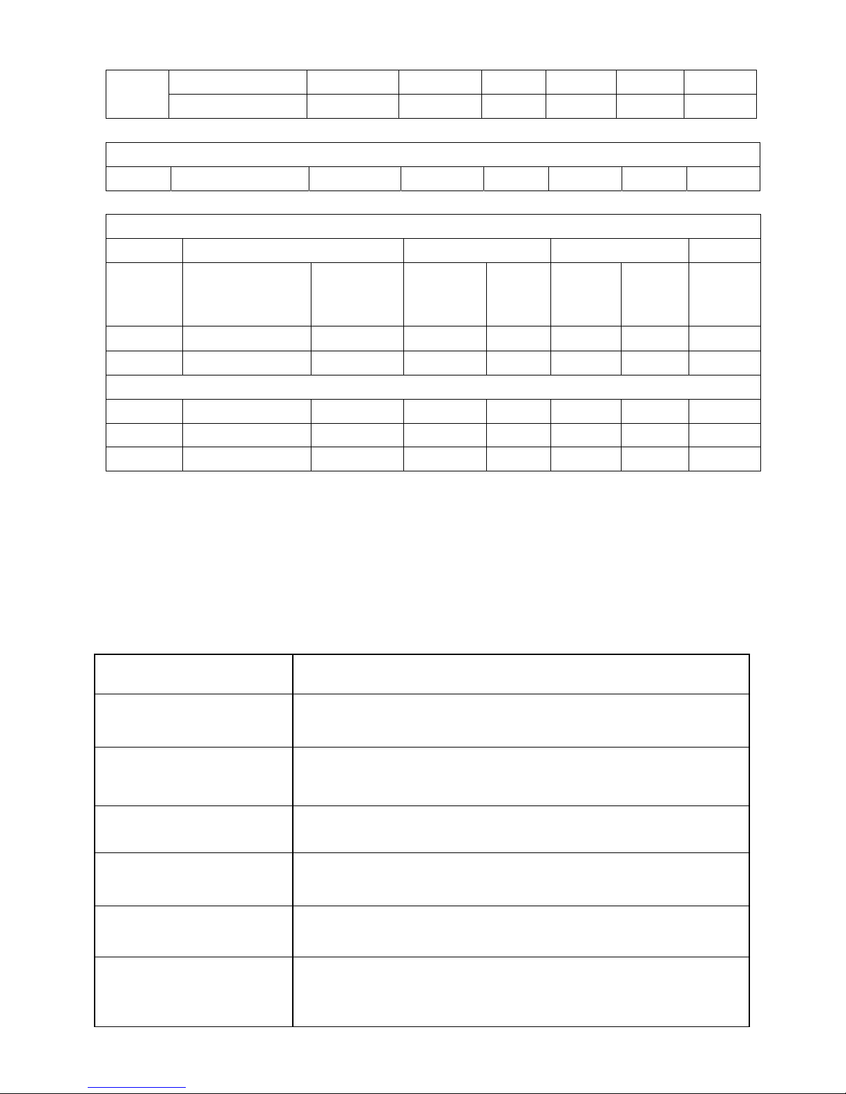
AD194TW TOSHIBA
Page 9 of 62
1152x864@75HZ 1600x900 67.500 P 75.000 P 108.00
***
1280x960@60HZ 1800x1000 60.000 P 60.000 P 108.00
NEC MODE
VGA 640x400@56Hz 848 x 440 24.827 N 56.424 N 21.052
IBM MODES
Horizontal Vertical
Mode Resolution Total
Nominal
Frequency
+/- 0.5kHz
Sync
Polarity
Nominal
Freq.
+/- 1 Hz
Sync
Polarity
Nominal
Pixel
Clock
(MHz)
DOS 720x400@70Hz 900 x 449 31.469 N 70.087 P 28.322
DOS 640x350@70Hz 800 x 449 31.469 P 70.087 N 25.175
MAC MODES
VGA 640x480@67Hz 864x525 35.000 N 66.667 N 30.240
SVGA 832x624@75Hz 1152x667 49.725 N 74.551 N 57.2832
XGA 1024x768@75Hz 1328X804 60.241 N 74.927 N 80.000
All modes will automatically optimize the screen size "AUTO-config" "function", except certain
screen pattern, such as only some characters display on black background.
4.3 POWER SUPPLY
4.3.1 INPUT/OUTPUT REQUIREMENTS
PARAMETER RANGE
AC Input Voltage 90 to 264V
AC Input Frequency 50 ± 3Hz, 60 ± 3Hz
AC Input Current 1.5A max
Inrush Current < 60A peak at 264 VAC and cold starting
Leakage Current < 3.5mA
Power line surge
No advance effects (no loss of information or defect)
with a maximum of 1 half-wave missing per second
AD194TW TOSHIBA
Page 10 of 62
4.3.2 INVERTER MAX BRIGHTNESS (Vadj:5.0v), LOAD=100KΩ x 4
(ROOM TEMPERATURE 25 ±4 )℃℃
ITEM SYMBOL MIN. TYP. MAX. UNIT REMARK
Input voltage Vin 10.8 12 13.2 V
Input current Iin 1700 1900 2100 mA FOR 4 LOAD
Output Current Iout 6.0 6.5 9.0 mA FOR 1 LOAD
Frequency F 40 48 80 KHZ FOR 1 LOAD
H.V open Vopen --- --- --- Vrms NO LOAD
H.V Load Vload 630 700 770 Vrms RL=100KΩ
Start voltage Vst 1430 --- --- Vrms RL=CCFL
Protect delay time PDT 1 --- 2 Sec
4.3.3 INVERTER MIN BRIGHTNESS (Vadj:0.0v), LOAD=100KΩ x 4
(ROOM TEMPERATURE 25℃ ±4℃)
ITEM SYMBOL MIN. TYP. MAX. UNIT REMARK
Input voltage Vin 10.8 12 13.2 V
Input current Iin 400 450 500 mA FOR 4 LOAD
Output Current Iout 3.5 4.0 4.5 mA FOR 1 LOAD
Frequency F 40 48 80 KHZ FOR 1 LOAD
Start voltage Vst 1430 --- --- Vrms RL=CCFL
Protect delay time PDT 1 --- 2 Sec
AD194TW TOSHIBA
Page 11 of 62
4.4 PANEL SPECIFICATION
4.4.1 General Feature
(HSD190ME13-A10 )
Parameter Specification
Outline dimension(mm) 396 * 324 * 17.5(Typ.)
Display area(mm) 376.32(H) x 301.056(V)(19.0” diagonal)
Number of Pixel
1280(H)x 1024(V)pixels
Pixel Pitch (mm)
0.294(H)x 0.294(V)
Pixel arrangement RGB vertical stripe
Display color 16.2M(6-bit+FRC)
Display mode Normally white
Surface treatment Antiglare, Hard-Coating(3H)
Weight(G) 2600(Typ.)
Back-light 4-CCFLs, Top & bottom edge side
Input signal 2-ch LVDS
System 3.05
Power consumption(W)
B/L 20
Optimum viewing direction 6 o’clock
Contrast ratio 550:1(typ.)
Viewing angle 150(H) x 135(V)
Response time 8ms(typ.)
Luminance 250cd/ m²
Power supply voltage LCD panel signal processing board:5V
AD194TW TOSHIBA
Page 12 of 62
4.4.2 OPTICAL CHARACTERISTICS
[Ta=25±2℃, VDD=5V, Fv =60Hz,Fdclk=54MKz, F IBL=6.5±0.1mArms/lamp,30min.Warm-up time.]
Item Symbol Condition Min Typ Max Unit Note
Contrast ratio CR 450 700 -- (1)(2)
Rising TR 2 4
Response time
Falling TF 6 8
msec (1)(3)
White Luminance
(center of screen)
YL 240 300 - cd/m²
(1)(4)(IL=6.5
mA)
Rx 0.614 0.644 0.674
Red
Ry 0.298 0.328 0.358
Gx 0.260 0.290 0.320
Green
Gy 0.584 0.614 0.644
Bx 0.112 0.142 0.172
Blue
By 0.049 0.079 0.109
Wx 0.280 0.310 0.340
Color
chromaticity
(CIE1931)
White
Wy
θ=0°
ф=0°
Normal
Viewing
angle
0.300 0.330 0.360
(1)(4)
Hor.
θL
65 75 --
Ver.
θR
65 75 --
Hor.
θH
55 70 --
Viewing angle
Ver.
θL
CR>10
55 65 --
Hor.
θL
-- 80 --
Ver.
θR
-- 80 --
Hor.
θH
-- 80 --
Viewing angle
Ver.
θL
CR>5
-- 80 --
Brightness uniformity BUNI
θ=0°
ф=0°
75 -- -- % (6)
AD194TW TOSHIBA
Page 13 of 62
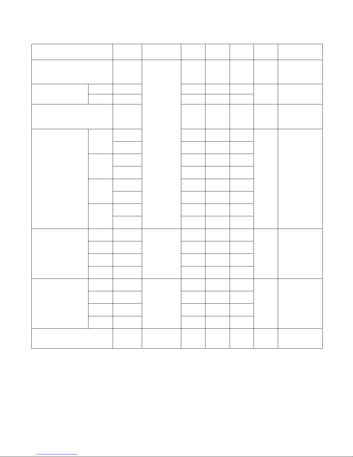
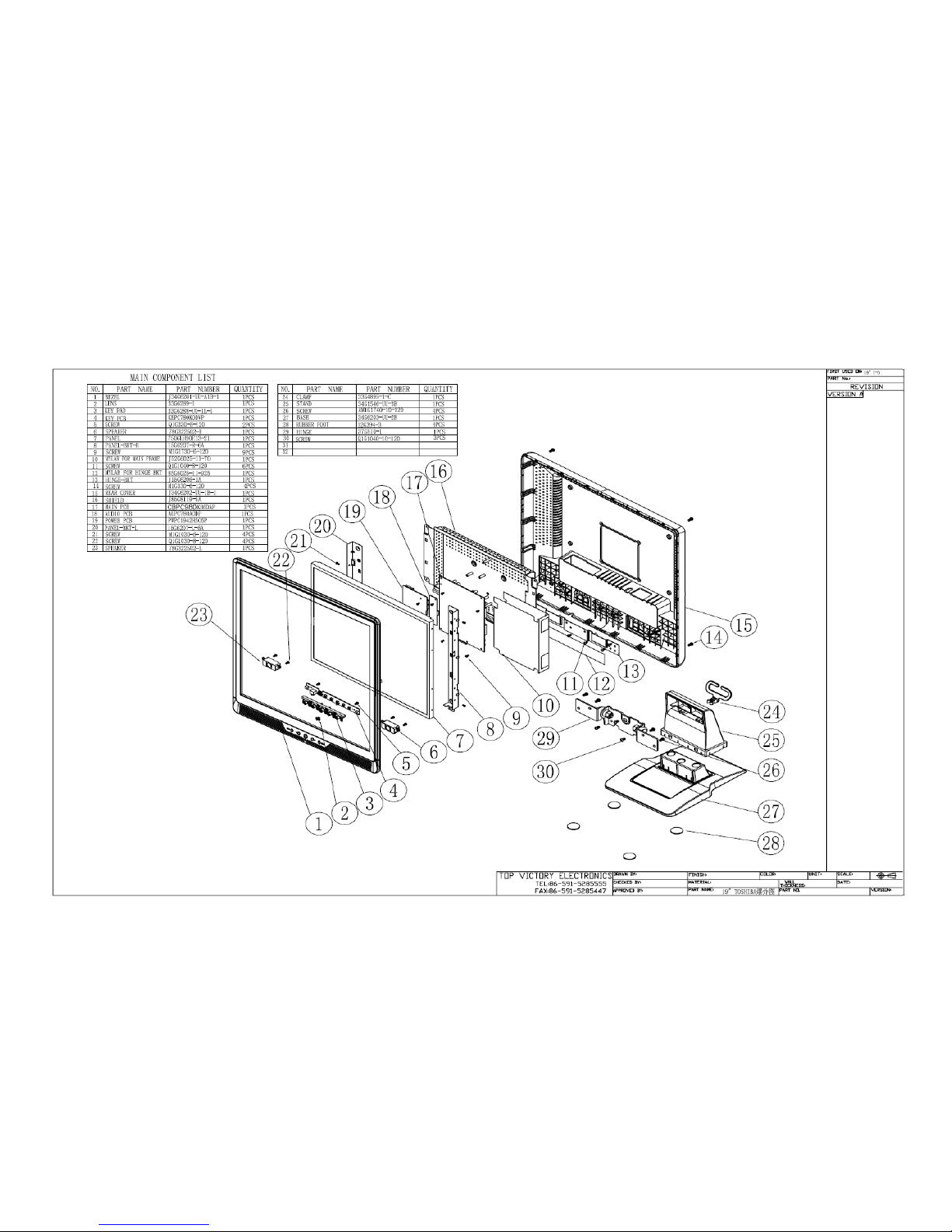
5. BLOCK DIAGRAM
5.1 MONITOR EXPLODED VIEW
AD194TW TOSHIBA
Page 14 of 62
MAIN COMPONENT LIST
NO. Part Name Part Number Quantity
1 BEZEL J34G6201-UU-A1B-1 1PCS
2 LENS 33G6289-L 1PCS
3 KEY PAD 33G6288-UU-1L-1 1PCS
4 KEY PCB KEPC780KODVP 1PCS
5 SCREW Q1G330-6-120 2PCS
6 SPEAKER 78G322-502-R 1PCS
7 PANEL 750GLH90E13-21 1PCS
8 PANEL-BKT-R 15G6207-R-6A 1PCS
9 SCREW M1G1730-6-120 9PCS
10 MYLAR FOR MAIN FRAME J52G6025-11-TO 1PCS
11 SCREW Q1G1040-8-120 6PCS
12 MYLAR FOR HINGE BKT 85G6025-11-925 1PCS
13 HINGE-BKT 15G6206-1A 1PCS
14 SCREW M1G330-6-120 4PCS
15 REAR COVER J34G6202-UU-1B-1 1PCS
16 SHIELD J85G8119-5A 1PCS
17 MAIN PCB CBPC980KH6DAP 1PCS
18 AUDIO PCB AUPC780A0DP 1PCS
19 POWER PCB PWPC1942HS05P 1PCS
20 PANEL-BKT-L 15G6207-L-3 1PCS
21 SCREW M1G1030-6-120 4PCS
22 SCREW Q1G1030-8-120 4PCS
23 SPEAKER 78G322502-L 1PCS
STAND Ass’y LIST
24 CLAMP 33G4895-1-C 1PCS
25 STAND 34G1546-UU-3B 1PCS
26 SCREW AM1G1740-10-120 4PCS
27 BASE 34G6203-UU-2B 1PCS
28 RUBBER FOOT 12G394-3 4PCS
29 HINGE 37G510-1 1PCS
30 SCREW Q1G1040-10-120 3PCS
AD194TW TOSHIBA
Page 15 of 62
5.2 DISASSEMBLE PROCESS
5.2.1 Tools:
Glove
Cross screwdriver
Six angle sleeve spanner
Prize equipment or abandoned IC card
Screw box
Cloth cushion
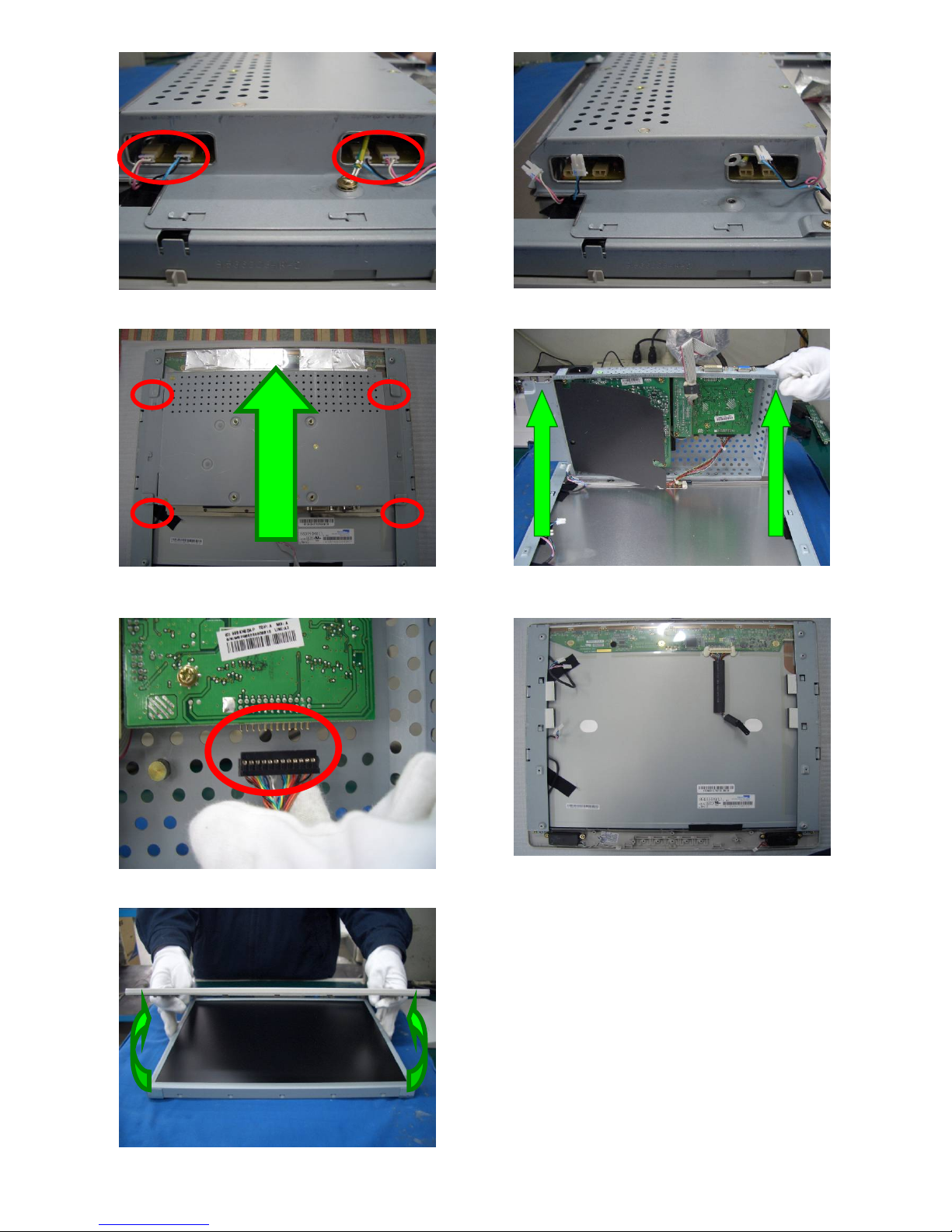
5.2.2 Disassemble process:
1 、 Tidy up the worktable, spread the cushion, put the monitor on it ,the front side
downwards.(Fig.1)
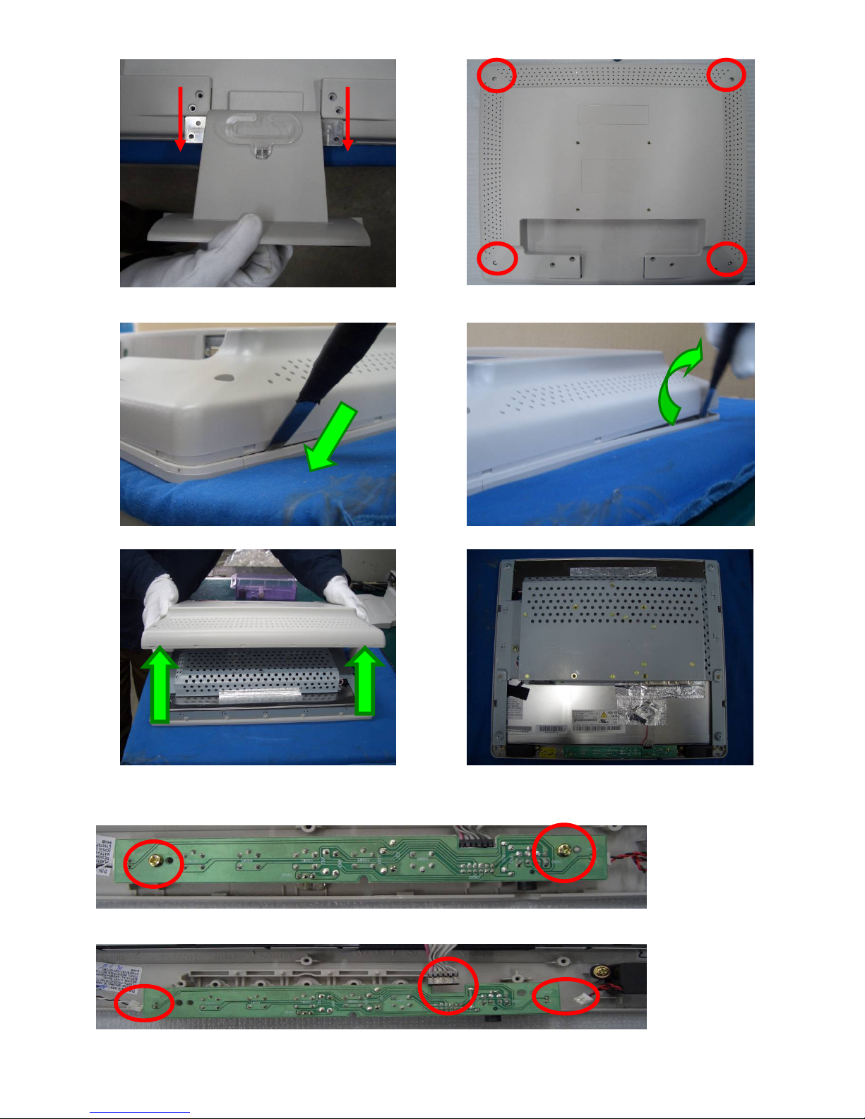
2、 Disassemble the fixed 4 screws of the stand, showed in Fig.2. Remove the base and
stand following the direction the arrowhead showed, refer to Fig.3.
3、 Disassemble the fixed 4 screws of the back cover, refer to Fig.4.
4、 Insert plastic card or abandoned IC card in the bottom of the monitor, between the bezel
and back cover, and remove the back cover. Refer to Fig.5,6,7,8.
5、 Disassemble the fixed 2 screws and 3 connect pins of the KEPC board, showed in Fig.
9,10.
6、 Disassemble 4 screws and 4 pins that fix the shield, refer to Fig.11,12, and remove the
shield following the direction arrowhead showed, Fig.13 ,14.
7、 Disassemble connect pins of the main board to panel, showed in Fig.15,16.
8、 Remove the bezel, showed in Fig.17. Do not scratch the panel.
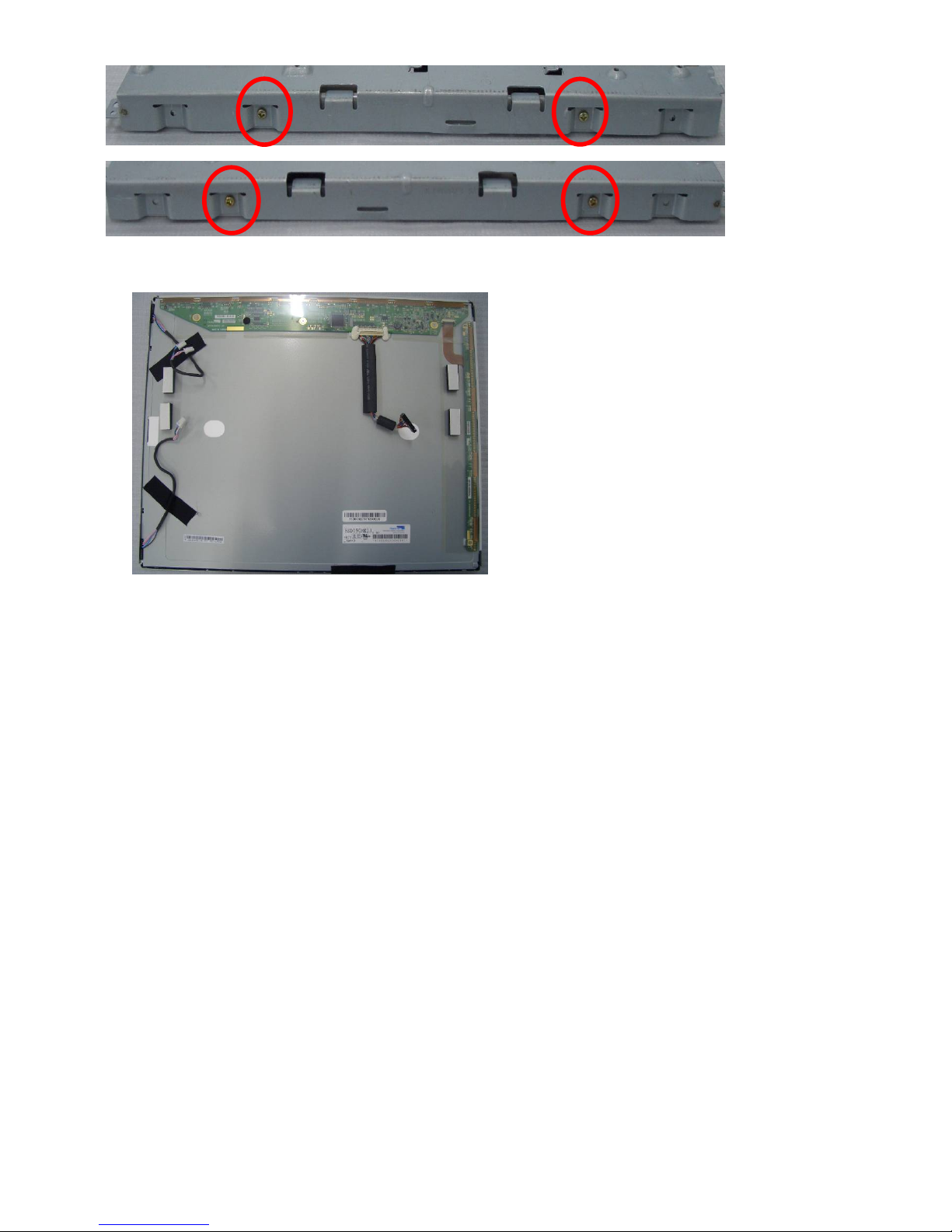
9、 Disassemble the screws that fix the panel, showed in Fig.18,19.
10、That’all, the process is over.
5.2.3 Pictures:
(Fig.1) (Fig.2)
Cushion
AD194TW TOSHIBA
Page 16 of 62
(Fig.3) (Fig.4)
(Fig.5) (Fig.6)
(Fig.7) (Fig.8)
(Fig.9)
(Fig.10)
AD194TW TOSHIBA
Page 17 of 62
(Fig.11) (Fig.12)
(Fig.13) (Fig.14)
(Fig.15) (Fig.16)
(Fig.17)
AD194TW TOSHIBA
Page 18 of 62
(Fig.18)
(Fig.19)
(Fig.20)
AD194TW TOSHIBA
Page 19 of 62
5.3 SOFTWARE FLOW CHART
1
2
N
Y
5
Y
N
10
Y
N
12
Y
N
7
Y
N
6
4
389
14
11
13
Y
N
1
5
Y
N
16
1
7
19
Y
N
18
 Loading...