

Toshiba TLCS-900/H1, TMP92CH21FG, JTMP92CH21 Series Manual
TOSHIBA Original CMOS 32-Bit Microcontroller
TLCS-900/H1 Series
TMP92CH21FG
Semiconductor Company

Preface
Thank you very much for making use of Toshiba microcomputer LSIs.
Before use this LSI, refer the section, “Points of Note and Restrictions”.

CMOS 32-bit Microcontroller
TMP92CH21FG/JTMP92CH21
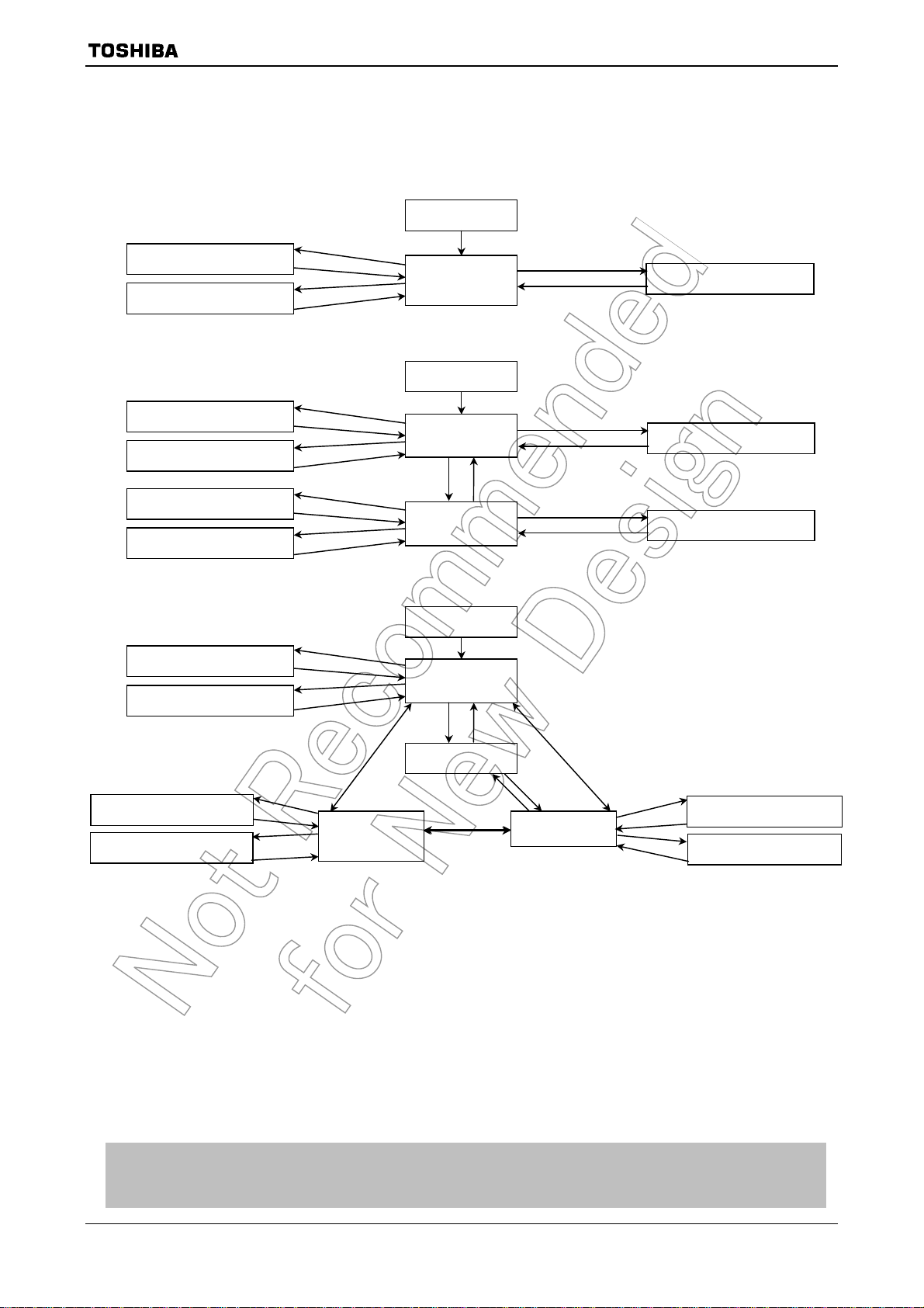
1. Outline and Device Characteristics
The TMP92CH21 is a high-speed advanced 32-bit Microcontroller developed for controlling
equipment which processes mass data.
The TMP92CH21 has a high-performance CPU (900/H1 CPU) and various built-in I/Os.
The TMP92CH21FG is housed in a 144-pin flat package. The JTMP92CH21 is a chip form
product.
Device characteristics are as follows:
(1) CPU: 32-bit CPU (900/H1 CPU)
• Compatible with TLCS-900/L1 instruction code
• 16 Mbytes of linear address space
• General-purpose register and register banks
TMP92CH21
• Micro DMA: 8 channels (250 ns/4 bytes at f
(2) Minimum instruction execution time: 50 ns (at f
= 20 MHz, best case)
SYS
= 20 MHz)
SYS
(3) Internal memory
• Internal RAM: 16 Kbytes (can be used for program, data and display memory)
• Internal ROM: 8 Kbytes (used as boot program)
Possible downloading of user program through either USB,
UART or NAND flash.
(4) External memory expansion
• Expandable up to 512 Mbytes (shared program/data area)
• Can simultaneously support 8,- 16- or 32-bit width external data bus
... dynamic data bus sizing
• Separate bus system
(5) Memory controller
• Chip select output: 4 channels
(6) 8-bit timers: 4 channels
(7) 16-bit timer/event counter: 1 channel
(8) General-purpose serial interface: 2 channels
• UART/synchronous mode: 2 channels (channel 0 and 1)
• IrDA ver.1.0 (115 kbps) mode selectable: 1 channel (channel 0)
92CH21-1
2009-06-19

(9) USB (universal serial bus) controller: 1 channel
• Compliant with USB ver.1.1
• Full-speed (12 Mbps) (Low-speed is not supported.)
• Endpoints spec
Endpoint 0: Control 64 bytes* 1-FIFO
Endpoint 1: BULK (out) 64 bytes* 2-FIFO
Endpoint 2: BULK (in) 64 bytes* 2-FIFO
Endpoint 3: Interrupt (in) 8 bytes* 1-FIFO
• Descriptor RAM: 384 bytes
2
S (Inter-IC sound) interface: 1 channel
(10) I
2
S bus mode/SIO mode selectable (Master, transmission only)
• I
• 32-byte FIFO buffer
(11) LCD controller
• Supports up to 4096 color for TFT, 256 color, 16, 8, 4 gray levels and B/W for STN
• Shift register/built-in RAM LCD driver
TMP92CH21
(12) SDRAM controller: 1 channel
• Supports 16 M, 64 M, 128 M, 256 M, and up to 512-Mbit SDR (Single Data Rate)-SDRAM
• Possible to execute instruction on SDRAM
(13) Timer for real-time clock (RTC)
(14) Key-on wakeup (Interrupt key input)
(15) 10-bit AD converter: 4 channels
(16) Touch screen interface
• Available to reduce external components
(17) Watchdog timer
(18) Melody/alarm generator
• Melody: Output of clock 4 to 5461 Hz
• Alarm: Output of 8 kinds of alarm pattern and 5 kinds of interval interrupt
(19) MMU
• Expandable up to 512 Mbytes (3 local area/8 bank method)
• Independent bank for each program, read data, write data and LCD display data
(20) Interrupts: 50 interrupt
• 9 CPU interrupts: Software interrupt instruction and illegal instruction
• 34 internal interrupts: Seven selectable priority levels
• 7 external interrupts: Seven selectable priority levels (6-edge selectable)
(21) Input/output ports: 82 pins (Except Data bus (16bit), Address bus (24bit) and
(22) NAND flash interface: 2 channels
• Direct NAND flash connection capability
• ECC calculation (for SLC- type)
92CH21-2
RD pin)
2009-06-19
TMP92CH21
(23) Stand-by function
• Three HALT modes: IDLE2 (programmable), IDLE1, STOP
• Each pin status programmable for stand-by mode
(24) Triple-clock controller
• Clock doubler (PLL) supplies 48 MHz for USB, 36 MHz system-clock for others
• Clock gear function: Select high-frequency clock fc to fc/16
• RTC (fs = 32.768 kHz)
(25) Operating voltage:
• VCC = 3.0 V to 3.6 V (fc max = 40 MHz)
• VCC = 2.7 V to 3.6 V (fc max = 27 MHz)
(26) Package:
• 144-pin QFP (LQFP144-P-1616-0.40C)
• 144-pin chip form is also available. For details, contact your local Toshiba sales
representative.
92CH21-3
2009-06-19
(
)
Y
(
)
A
A
(
,
)
AN3/MY/
(TXD0, TXD1) PF0
(RXD0, RXD1) PF1
(SCLK0,SCLK1) PF2
(I2SCKO, TXD0) P90
(I2SWS, SCLK0,
(I2SDO, RXD0) P91
(LGOE2, CLK32KO) P95
(TA1OUT, INT0) PC0
(TA3OUT, INT1) PC1
(TB0OUT0, INT2) PC2
(
SDRAS ,SRLLB ) PJ0
SDCAS ,SRLUB ) PJ1
(
SDWE ,SRWR ) PJ2
(
(NDALE, SDULDQM) PJ5
(NDCLE, SDUUDQM) PJ6
PG0 to PG1
(AN0 to AN1)
AN2/MX (PG2)
ADTRG (PG3)
AVCC, AVSS
VREFH, VREFL
(PX, INT4) P96
(PY, INT5) P97
D+
D−
0CTS ) P92
(LGOE0) P93
(LGOE1) P94
(INT3) PC3
(LCP0) PK0
(LLP) PK1
(LFR) PK2
(LBCD) PK3
PL0 to PL7
LD0 to LD7
(SDLLDQM) PJ3
(SDLUDQM) PJ4
(SDCKE) PJ7
(SDCLK) PF7
10-bit
4-channel
AD converter
Touch
screen
I/F (TSI)
Serial I/O
SIO0
Serial I/O SIO1
USB
controller
I2S
Port 9
8-bit timer
(TIMERA0)
8-bit timer
(TIMERA1)
8-bit timer
(TIMERA2)
8-bit timer
(TIMERA3)
16-bit timer
(TIMERB0)
LCD
controller
SDRAM
controller
900/H1 CPU
XWA
XBC
XDE
XHL
XIX
XIY
XIZ
XSP
32 bits
SR
Watchdog timer
MMU
16-KB RAM
8-KB mask ROM
(Boot program)
WA
BC
DE
HL
PC
IX
I
IZ
SP
F
PLL
H-OSC
Clock gear
L-OSC
Interrupt
controller
Port 1
Port 2
Port 3
Port 4
Port 5
Port 6
Port 7
NAND flash
I/F (2 channel)
Port 8
Keyboard
I/F
RTC
Melody/
Alarm out
TMP92CH21
DVCC [4]
DVSS [3]
X1
X2
TEST
XT1
XT2
RESET
M0
M1
D0 to D7
P10 to P17
(D8 to D15)
P20 to P27
(D16 to D23, KO0 to KO7)
P30 to P37
(D24 to D31)
P40 to P47
(A0 to A7)
P50 to P57
(A8 to A15)
P60 to P67
(A16 to A23)
RD
P70 (
P71 (
P72 (
P73 (EA24)
P74 (EA25)
P75 (R/
P76 (
P80 (
P81 (
P82 (
P83 (
P84 (
P85 (
P86 (
P87 (
PC7
PA0 to PA7 (KI0 to KI7,
PC6
PM2 (
PM1 (MLDALM)
)
WRLL , NDRE )
WRLU , NDWE )
W , NDR/B)
WAIT )
0CS )
1CS , SDCS )
2CS , CSZA , SDCS )
3CS )
CSZB , WRUL , CE0ND )
CSZC , WRUU , CE1ND )
CSZD , SRULB )
CSZE , SRUUB )
CSZF
LCP1
LD8 to LD11)
KO8, LDIV
ALARM , MLDALM )
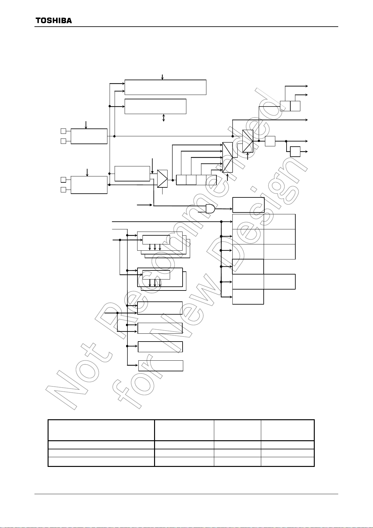
Figure 1.1 TMP92CH21 Block Diagram
92CH21-4
2009-06-19
A
2. Pin Assignment and Functions
The assignment of input/output pins for the TMP92CH21FG, their names and functions are
as follows:
2.1 Pin Assignment
SDWE, SRWR
SDCAS, SRLUB
VCC AVSS
PA2, KI2
PA1, KI1
PA0, KI0
PJ7, SDCKE
PJ6, SDUUDQM, NDCLE
PJ5, SDULDQM, NDALE
PJ4, SDLUDQM
PJ3, SDLLDQM
PJ1,
PJ2,
SDRAS, SRLLB
PJ0,
PF7, SDCLK
PC1, TA3OUT, INT1
TMP92CH21
CTS0, SCLK1, CTS1
CSZF, LCP1
CSZE, SRUUB
CSZD, SRULB
CSZC, WRUU, ND1CE
CSZB, WRUL, ND0CE
CS3
CS2, CSZA, SDCS
CS1, SDCS
CS0
WAIT
WRLU, NDWE
WRLL, NDRE
RD
P87,
P84,
P83,
P81,
P75, R/W, NDR/B
PC6, KO8, LDIV
PF1, RXD0, RXD1
PF0, TXD0, TXD1
PC7,
P86,
PC0, TA1OUT, INT0
PF2, SCLK0,
P85,
P82,
P80,
P76,
P74, EA25
P73, EA24
P72,
P71,
P70,
PG0, AN0
PG1, AN1
PG2, AN2, MX
PG3, AN3,
P92, SCLK0,
P95, CLK32KO, LGOE2
PM2,
ADTRG , MY
P96, PX, INT4
P97, PY, INT5
PA3, KI3, LD8
PA4, KI4, LD9
PA5, KI5, LD10
PA6, KI6, LD11
P90, TXD0, I2SCKO
P91, RXD0, I2SDO
P93, LGOE0
P94, LGOE1
PC2, TB0OUT0, INT2
PK0, LCP0
PK3, LBCD
ALARM , MLDALM
PM1, MLDALM
VREFL
VREFH
PA7, KI7
0CTS , I2SWS
PL0, LD0
PL1, LD1
PL2, LD2
PL3, LD3
PL4, LD4
PL5, LD5
PL6, LD6
PL7, LD7
PK1, LLP
PK2, LFR
XT1
XT2
1
5
10
15
20
25
30
35
140
40
135
45
130
125
TMP92CH21FG
QFP144
Top View
50
55
120
60
115
65
70
110
105
100
P67, A23
P66, A22
P65, A21
P64, A20
DVCC3
P63, A19
P62, A18
P61, A17
P60, A16
P57, A15
P56, A14
P55, A13
95
90
85
80
75
P54, A12
P53, A11
P52, A10
P51, A9
P50, A8
P47, A7
P46, A6
P45, A5
P44, A4
P43, A3
P42, A2
P41, A1
P40, A0
P37, D31
P36, D30
DVSS3
P35, D29
P34, D28
P33, D27
P32, D26
P31, D25
P30, D24
P27, D23, KO7
P26, D22, KO6
X1
D+
TEST
DVCC4
X2
D−
DVCC1
AM0
DVSS1
AM1
RESET
PC3, INT3
DVSS2
D0D1D2D3D4D5D6
DVCC2
D7
P10, D8
P11, D9
P12, D10
P13, D11
P14, D12
P15, D13
P16, D14
P17, D15
P20, D16, KO0
P21, D17, KO1
P22, D18, KO2
P23, D19, KO3
P24, D20, KO4
P25, D21, KO5
Figure 2.1.1 Pin Assignment Diagram (144-pin QFP)
92CH21-5
2009-06-19
TMP92CH21
2.2 P AD Assignment
(Chip size 5.98 mm × 6.42 mm)
Table 2.2.1 Pad Assignment Diagram (144-pin chip)
Unit: μm
Pin
No
1
2
3
4
5
6
7 P96 −2852 1920 55 D4 300 −3072 103 P63 2848 1566
8 P97 −2852 1795 56 D5 425 −3072 104 DVCC3 2848 1692
9 PA3
10 PA4 −2852 1145 58 D7 675 −3072 106 P65 2848 1974
11 PA5 −2852 1020 59 P10 800 −3072 107 P66 2848 2130
12 PA6 −2852 895 60 P11 925 −3072 108 P67 2848 2292
13 PA7 −2852 769 61 P12 1050 −3072 109 P70 2460 3065
14 P90 −2852 644 62 P13 1176 −3072 110 P71 2295 3065
15 P91 −2852 519 63 P14 1301 −3072 111 P72 2127 3065
16 P92 −2852 394 64 P15 1426 −3072 112 P73 1964 3065
17 P93 −2852 269 65 P16 1551 −3072 113 P74 1807 3065
18 P94 −2852 144 66 P17 1676 −3072 114 P75 1654 3065
19 P95 −2852 18 67 P20 1801 −3072 115 P76 1506 3065
20 PC2 −2852 −106 68 P21 1927 −3072 116 P80 1361 3065
21 PL0 −2852 −231 69 P22 2052 −3072 117 PC6 1226 3065
22 PL1 −2852 −356 70 P23 2177 −3072 118 P81 1101 3065
23 PL2 −2852 −481 71 P24 2303 −3072 119 P82 976 3065
24 PL3 −2852 −606 72 P25 2460 −3072 120 P83 851 3065
25 PL4
26 PL5 −2852 −857 74 P27 2848 −2138 122 P85 600 3065
27 PL6 −2852 −982 75 P30 2848 −1982 123 P86 475 3065
28 PL7 −2852 −1107 76 P31 2848 −1831 124 P87 350 3065
29 PK0 −2852 −1232 77 P32 2848 −1687 125 PC7 225 3065
30 PK1 −2852 −1357 78 P33 2848 −1562 126 PF0 100 3065
31 PK2 −2852 −1482 79 P34 2848 −1437 127 PF1 −24 3065
32 PK3 −2852 −1608 80 P35 2848 −1311 128 PF2 −150 3065
33 PM2 −2852 −1892 81 DVSS3 2848 −1186 129 PC0 −275 3065
34 PM1
35 XT1
36 XT2
37 DVCC4
38
39 D+
40 D−
41 DVCC1
42 X1
43 DVSS1
44 X2
45 AM0
46 AM1
47
48 PC3
Name
VREFL
VREFH
PG0
PG1
PG2
PG3 −2852 2045
TEST
RESET
X
Point Y Point
−2852 2671 49 DVSS2 −488 −3072 97 P55 2848 815
−2852 2546 50 DVCC2 −338 −3072 98 P56 2848 941
−2852 2421
−2852 2296 52 D1 −75 −3072 100 P60 2848 1191
−2852 2171 53 D2 49 −3072 101 P61 2848 1316
−2852 1270
−2852 −732
−2852 −2017
−2852 −2142
−2852 −2444
−2465 −3072
−2339 −3072
−2062 −3072
−1875 −3072
−1598 −3072
−1472 −3072
−1347 −3072
−1126 −3072
−1001 −3072
−876 −3072
−750 −3072
−625 −3072
Pin
No
51 D0
54 D3
57 D6
73 P26
82 P36
83 P37
84 P40
85 P41
86 P42
87 P43
88 P44
89 P45
90 P46
91 P47
92 P50
93 P51
94 P52
95 P53
96 P54
Name
X
Point Y Point
−200 −3072
174 −3072
550 −3072
2848 −2279
2848 −1061
2848 −936
2848 −811
2848 −686
2848 −560
2848 −435
2848 −310
2848 −185
2848 −60
2848 65
2848 190
2848 315
2848 440
2848 565
2848 690
Pin
No
99 P57
102 P62
105 P64
121 P84
130 PC1 −400 3065
131 PF7 −525 3065
132 PJ0 −650 3065
133 PJ1 −775 3065
134 PJ2 −901 3065
135 PJ3 −1026 3065
136 PJ4 −1151 3065
137 PJ5 −1276 3065
138 PJ6 −1401 3065
139 PJ7 −1526 3065
140 PA0 −1652 3065
141 PA1 −1777 3065
142 PA2 −1902 3065
143 AVSS −2275 3065
144 AVCC −2400 3065
Name
X
Point Y Point
2848 1066
2848 1441
2848 1823
726 3065
92CH21-6
2009-06-19
2.3 Pin Names and Functions
The following table shows the names and functions of the input/output pins
Table 2.3.1 Pin Names and Functions (1/5)
TMP92CH21
Pin Name
Number of
I/O Function
Pins
D0 to D7 8 I/O Data: Data bus 0 to 7
P10 to P17
D8 to D15
P20 to P27
D16 to D23
KO0 to KO7
P30 to P37
D24 to D31
P40 to P47
A0 to A7
P50 to P57
A8 to A15
P60 to P67
A16 to A23
P70
RD
P71
WRLL
NDRE
P72
WRLU
NDWE
P73
EA24
P74
EA25
P75
WR/
NDR/B
P76
WAIT
8
8
8
8
8
8
1
1
1
1
1
1
1
I/O
I/O
I/O
I/O
Output
I/O
I/O
Output
Output
Output
Output
I/O
Output
Output
Output
I/O
Output
Output
I/O
Output
Output
Output
Output
Output
Output
I/O
Output
Input
I/O
Input
Port 1: I/O port input or output specifiable in units of bits
Data: Data bus 8 to 15
Port 2: I/O port input or output specifiable in units of bits
Data: Data bus 16 to 23
Key output 0 to 7: Pins used of key-scan strobe (Open-drain output programmable)
Port 3: I/O port input or output specifiable in units of bits
Data24: Data bus 24 to 31
Port 4: Output port
Address: Address bus 0 to 7
Port 5: Output port
Address: Address bus 8 to 15
Port 6: I/O port input or output specifiable in units of bits
Address: Address bus 16 to 23
Port70: Output port
Read: Outputs strobe signal to read external memory
Port 71: I/O port
Write: Output strobe signal for writing data on pins D0 to D7
NAND flash read: Outputs strobe signal to read external NAND flash
Port 72: I/O port
Write: Output strobe signal for writing data on pins D8 to D15
Write Enable for NAND flash
Port 73: Output port
Extended Address 24
Port 74: Output port
Extended Address 25
Port 75: I/O port
Read/Write: 1 represents read or dummy cycle; 0 represents write cycle
NAND flash ready (1)/Busy (0) input
Port 76: I/O port
Wait: Signal used to request CPU bus wait
92CH21-7
2009-06-19
TMP92CH21
Table 2.3.2 Pin Names and Functions (2/5)
Pin Name
P80
0CS
P81
1CS
SDCS
P82
2CS
CSZA
SDCS
P83
3CS
P84
WRUL
CSZB
CE0ND
P85
WRUU
CSZC
CE1ND
P86
CSZD
SRULB
P87
CSZE
SRUUB
P90
TXD0
I2SCKO
P91
RXD0
I2SDO
P92
SCLK0
0CTS
I2SWS
P93
LGOE0
P94
LGOE1
P95
CLK32KO
LGOE2
P96
INT4
PX
P97
INT5
PY
PA0 to PA2
KI0 to KI2
PA3 to PA6
KI3 to KI6
LD8 to LD11
PA7
KI7
Number of
Pins
1
1
1
1
1
1
1
1
1
1
1
1
1
1
1 Input
1 Input
3
4
1
Output
Output
Output
Output
Output
Output
Output
Output
Output
Output
Output
Output
Output
Output
Output
Output
Output
Output
Output
Output
Output
Output
Output
Output
Output
Output
Output
Output
Output
Output
Output
Output
Output
Output
Output
Output
Output
I/O Function
Port80: Output port
Chip select 0: Outputs “low” when address is within specified address area
Port81: Output port
Chip select 1: Outputs “low” when address is within specified address area
Chip select for SDRAM: Outputs “0” when address is within SDRAM address area
Port82: Output port
Chip select 2: Outputs “Low” when address is within specified address area
Expand chip select: ZA: Outputs “0” when address is within specified address area
Chip select for SDRAM: Outputs “0” when address is within SDRAM address area
Port83: Output port
Chip select 3: Outputs “low” when address is within specified address area
Port84: Output port
Write: Output strobe signal for writing data on pins D16 to D23
Expand chip select: ZB: Outputs “0” when address is within specified address area
Chip select for NAND flash 0: Outputs “0” when NAND flash 0 is enabled
Port85: Output port
Write: Output strobe signal for writing data on pins D24 to D31
Expand chip select: ZC: Outputs “0” when address is within specified address area
Chip select for NAND flash 1: Outputs “0” when NAND flash 1 is enabled
Port86: Output port
Expand chip select: ZD: outputs “0” when address is within specified address area
Data enable for SRAM on pins D16 to D23
Port87: Output port
Expand chip select: ZE: Outputs “0” when address is within specified address area
Data enable for SRAM on pins D24 to D31
I/O
Port90: I/O port
Serial 0 send data: Open-drain output programmable
2
I
S clock output
I/O
Port91: I/O port (Schmitt-input)
Input
Input
Input
Input
Input
Input
Input
Input
Input
Input
Serial 0 receive data
2
I
S data output
I/O
Port92: I/O port (Schmitt-input)
I/O
Serial 0 clock I/O
Serial 0 data send enable (Clear to send)
2
I
S word select output
I/O
Port93: I/O port
Output enable-0 for external TFT-LCD driver
I/O
Port94: I/O port
Output enable-1 for external TFT-LCD driver
Port95: Output port
Output fs (32.768 kHz) clock
Output enable-2 for external TFT-LCD driver
Port 96: Input port (Schmitt-input)
Interrupt request pin4: Interrupt request with programmable rising/falling edge
X-Plus: Pin connectted to X+ for touch screen panel
Port 97: Input port (Schmitt-input)
Interrupt request pin5: Interrupt request with programmable rising/falling edge
Y-Plus: Pin connectted to Y+ for touch screen panel
Port: A0 to A2 port: Pin used to input ports (Schmitt input, with pull-up resistor)
Key input 0 to 2: Pin used for key-on wakeup 0 to 2
Port: A3 to A6 port: Pin used to input ports (Schmitt input, with pull-up resistor)
Key input 3 to 6: Pin used for key-on wakeup 3 to 6
Data bus 8 to 11for LCD driver
Port: A7 port: Pin used to input ports (Schmitt input, with pull-up resistor)
Key input 7: Pin used for key-on wakeup 7
92CH21-8
2009-06-19
TMP92CH21
Table 2.3.3 Pin Names and Functions (3/5)
Pin Name
PC0
INT0
TA1OUT
PC1
INT1
TA3OUT
PC2
INT2
TB0OUT0
PC3
INT3
PC6
KO8
LDIV
PC7
CSZF
LCP1
PF0
TXD0
TXD1
PF1
RXD0
RXD1
PF2
SCLK0
0CTS
SCLK1
1CTS
PF7
SDCLK
PG0 to PG1
AN0 to AN1
PG2
AN2
MX
PG3
AN3
MY
ADTRG
Number of
Pins
1
1
1
1
1
1
1
1
1
1
2
1
1
I/O Function
I/O
Port C0: I/O port (Schmitt-input)
Input
Output
Input
Output
Input
Output
Input
Output
Output
Output
Output
Output
Output
Input
Input
Input
Input
Output
Output
Input
Input
Input
Input
Output
Input
Input
Output
Intput
Interrupt request pin 0: Interrupt request pin with programmable level/rising/falling edge
8-bit timer 1 output: Timer 1 output
I/O
Port C1: I/O port (Schmitt-input)
Interrupt request pin 1: Interrupt request pin with programmable rising/falling edge
8-bit timer 3 output: Timer 3 output
I/O
Port C2: I/O port (Schmitt-input)
Interrupt request pin 2: Interrupt request pin with programmable rising/falling edge
Timer B0 output
I/O
Port C3: I/O port (Schmitt-input)
Interrupt request pin 3: Interrupt request pin with programmable rising/falling edge
I/O
Port C6: I/O port
Key Output 8: Pin used of key-scan strobe (Open-drain output programmable)
Data invert enable for external TFT-LCD driver
I/O
Port C7: I/O port
Expand chip select: ZF: Outputs “0” when address is within specified address area
Shift-clock-1 for external TFT-LCD driver
I/O
Port F0: I/O port (Schmitt-input)
Serial 0 send data: Open-drain output programmable
Serial 1 send data: Open-drain output programmable
I/O
Port F1: I/O port (Schmitt-input)
Serial 0 receive data
Serial 1 receive data
I/O
Port F2: I/O port (Schmitt-input)
I/O
Serial 0 clock I/O
Serial 0 data send enable (Clear to send)
I/O
Serial 1 clock I/O
Serial 1 data send enable (Clear to send)
Port F7: Output port
Clock for SDRAM (When SDRAM is not used, SDCLK can be used as system clock)
Port G0 to G1 port: Pin used to input ports
Analog input 0 to 1: Pin used to Input to AD conveter
Port G2 port: Pin used to input ports
Analog input 2: Pin used to Input to AD conveter
X-Minus: Pin connectted to X− for touch screen panel
Port G3 port: Pin used to input ports
Analog input 3: Pin used to input to AD conveter
Y-Minus: Pin connectted to Y− for touch screen panel
AD trigger: Signal used to request AD start
92CH21-9
2009-06-19
TMP92CH21
Table 2.3.4 Pin Names and Functions (4/5)
Pin Name
PJ0
SDRAS
SRLLB
PJ1
SDCAS
SRLUB
PJ2
SDWE
SRWR
PJ3
SDLLDQM
PJ4
SDLUDQM
PJ5
SDULDQM
NDALE
PJ6
SDUUDQM
NDCLE
PJ7
SDCKE
PK0
LCP0
PK1
LLP
PK2
LFR
PK3
LBCD
PL0 to PL3
LD0 to LD3
PL4 to PL7
LD4 to LD7
TEST
PM1
MLDALM
PM2
ALARM
MLDALM
Number of
Pins
1
1
1
1
1
1
1
1
1
1
1
1
4
4
1
1
1
I/O Function
Output
Output
Output
Output
Output
Output
Output
Output
Output
Output
Output
Output
Output
Output
Output
Output
Output
Output
Output
Output
Output
Output
Output
Output
Output
Output
Output
Output
Output
Output
Input Connect to VCC.
Output
Output
Output
Output
Output
Port J0: Output port
Row address strobe for SDRAM
Data enable for SRAM on pins D0 to D7
Port J1: Output port
Column address strobe for SDRAM
Data enable for SRAM on pins D8 to D15
Port J2: Output port
Write enable for SDRAM
Write for SRAM: Strobe signal for writing data
Port J3: Output port
Data enable for SDRAM on pins D0 to D7
Port J4: Output port
Data enable for SDRAM on pins D8 to D15
I/O
Port J5: I/O port
Data enable for SDRAM on pins D16 to D23
Address latch enable for NAND flash
I/O
Port J6: I/O port
Data enable for SDRAM on pins D24 to D31
Command latch enable for NAND flash
Port J7: Output port
Clock enable for SDRAM
Port K0: Output port
LCD driver output pin
Port K1: Output port
LCD driver output pin
Port K2: Output port
LCD driver output pin
Port K3: Output port
LCD driver output pin
Port L0 to L3: Output port
Data bus for LCD driver
I/O
Port L4 to L7: I/O port
Data bus for LCD driver
Port M1: Output port
Melody/alarm output pin
Port M2: Output port
RTC alarm output pin
Melody/alarm output pin (inverted)
Note: The output functions SDULDQM, NDALE of PJ5-pin and SDUUDQM, NDCLE of PJ6-pin cannot be
used simultaneously. Therefore, 32-bit SDRAM and NAND-Flash cannot be used at the same time.
92CH21-10
2009-06-19
TMP92CH21
Table 2.3.5 Pin Names and Functions (5/5)
Pin Name
D+, D− 2 I/O
AM0, AM1 2 Input
X1/X2 2 I/O High-frequency oscillator connection pins
XT1/XT2 2 I/O Low-frequency o scillator connection pins
RESET 1 Input Reset: Initializes TMP92CH21 (with pull-up resistor, Schmitt input)
VREFH 1 Input Pin for reference voltage input to AD converter (H)
VREFL 1 Input Pin for reference voltage input to AD converter (L)
AVCC 1 − Power supply pin for AD converter
AVSS 1 − GND pin for AD converter (0 V)
DVCC 4 − Power supply pins (All VCC pins should be connected to the power supply pin)
DVSS 3 − GND pins (0 V) (All pins should be connected to GND (0 V))
Number of
Pins
I/O Function
USB-data connecting pin
Connect pull-up resistor to both pins to avoid through current when USB is not in use.
Operation mode:
Fix to AM1 = “0”, AM0 = “1” for 16-bit external bus starting
Fix to AM1 = “1”, AM0 = “0” for 32-bit external bus starting
Fix to AM1 = “1”, AM0 = “1” for BOOT (32-bit internal MROM) starting
Note: Use a 9.0 MHz oscillator at pins X1/X2 when USB is used.
92CH21-11
2009-06-19
3. Operation
This section describes the basic components, functions and operation of the TMP92CH21.
3.1 CPU
The TMP92CH21 contains an advanced high-speed 32-bit CPU (TLCS-900/H1 CPU)
3.1.1 CPU Outline
The TLCS-900/H1 CPU is a high-speed, high-performance CPU based on the
TLCS-900/L1 CPU. The TLCS-900/H1 CPU has an expanded 32-bit internal data bus to
process instructions more quickly.
The following is an outline of the CPU:
Table 3.1.1 TMP92CH21 Outline
Parameter TMP92CH21
Width of CPU address bus 24 bits
Width of CPU data bus 32 bits
Internal operating frequency Max 20 MHz
Minimum bus cycle
Internal RAM 32-bit 1-clock access
1-clock access (50 ns at f
= 20MHz)
SYS
TMP92CH21
Internal boot ROM 32-bit 2-clock access
Internal I/O
External SRAM, Masked ROM
External SDRAM 16- or 32-bit min. 1-clock access
External NAND flash
Minimum instruction
execution cycle
Conditional jump
Instruction queue buffer 12 bytes
Instruction set
CPU mode Maximum mode only
Micro DMA 8 channels
8- or 16-bit 2-clock access or
8- or 16-bit 5 to 6-clock access
8- or 16- or 32-bit 2-clock access
(waits can be inserted)
8-bit min. 4-clock access
(waits can be inserted)
1-clock (50 ns at f
2-clock (100 ns at f
Compatible with TLCS-900/L1
(LDX instruction is deleted)
=20MHz)
SYS
=20MHz)
SYS
92CH21-12
2009-06-19
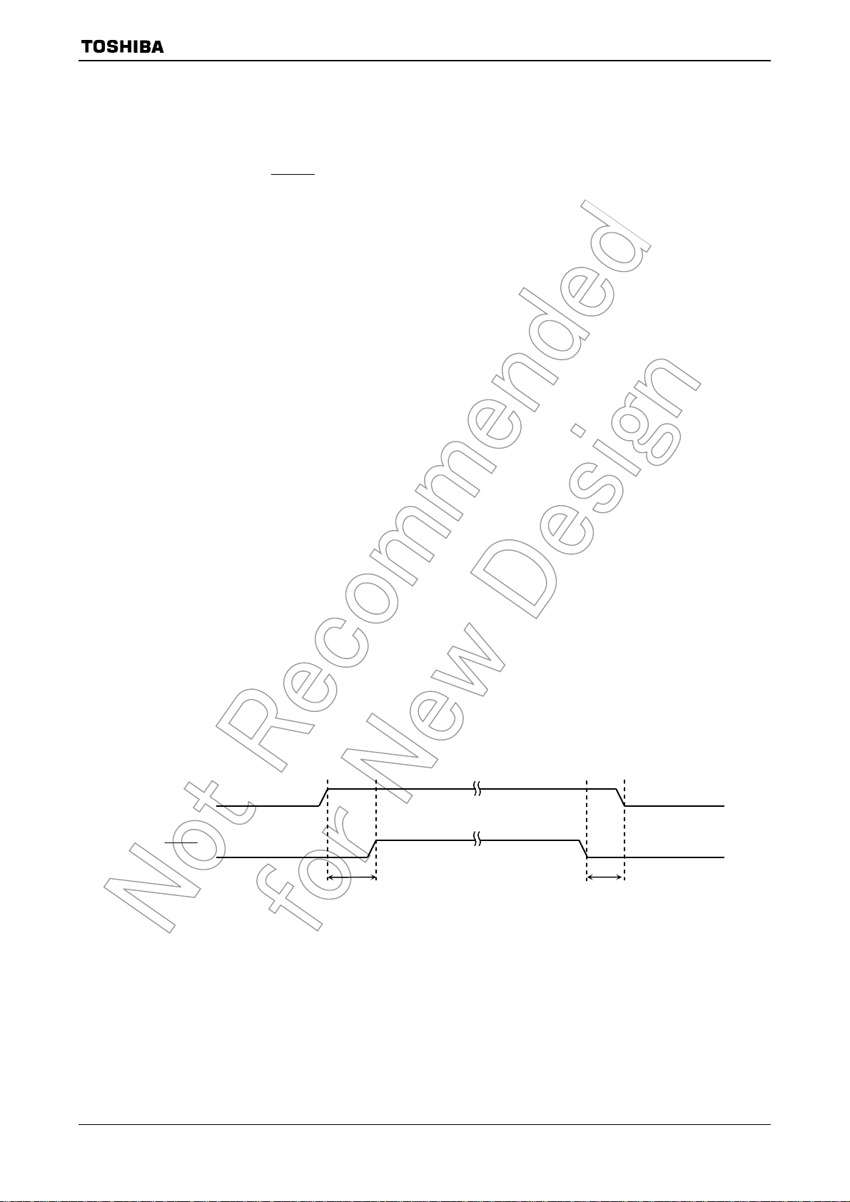
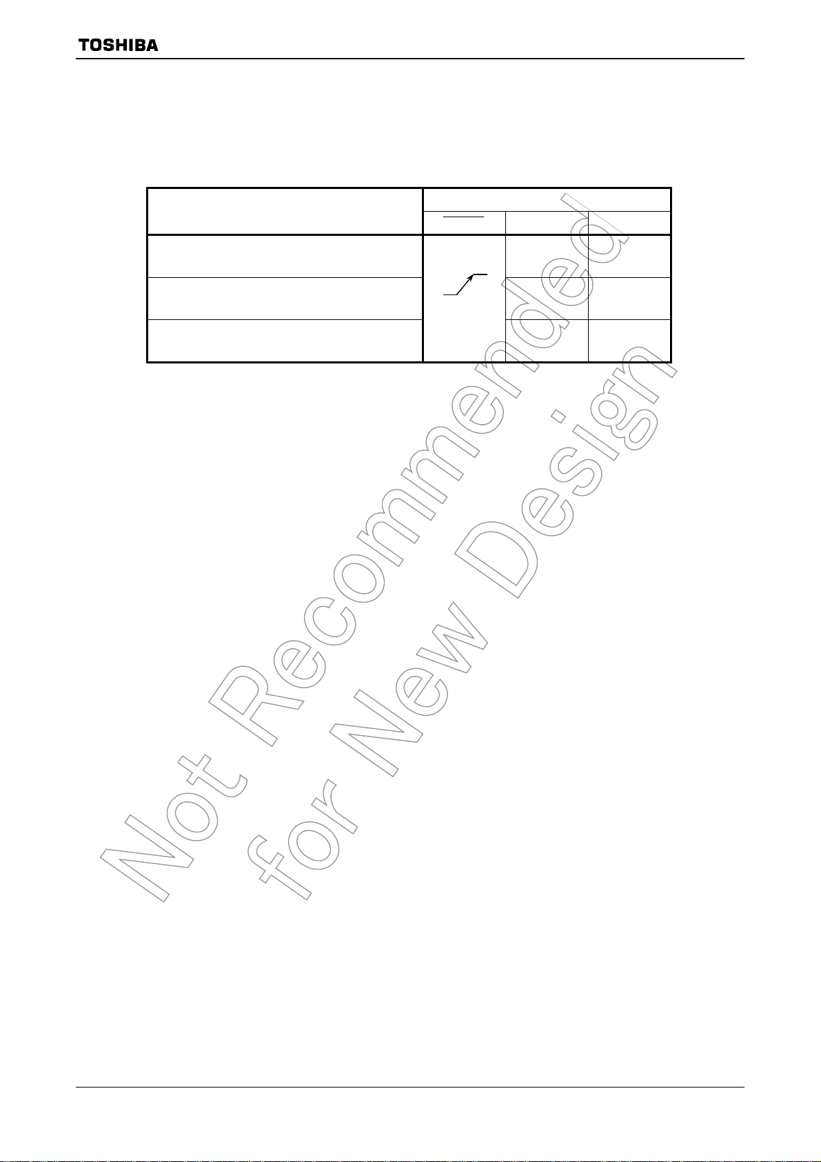
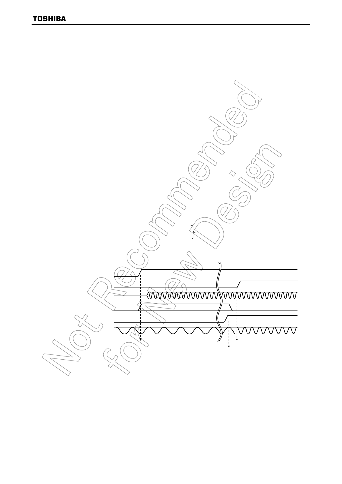
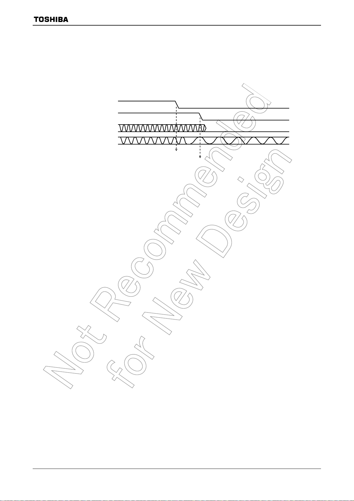
3.1.2 Reset Operation
When resetting the TMP92CH21, ensure that the power supply voltage is within the
operating voltage range, and that the internal high-frequency oscillator has stabilized.
Then hold the
At reset, since the clock doubler (PLL) is bypassed and the clock-gear is set to 1/16, the
system clock operates at 1.25 MHz (fc = 40 MHz).
When the reset has been accepted, the CPU performs the following:
• Sets the program counter (PC) as follows in accordance with the reset vector stored
• Sets the stack pointer (XSP) to 00000000H.
• Sets bits <IFF2:0> of the status register (SR) to 111 (thereby setting the interrupt
• Clears bits <RFP1:0> of the status register to 00 (there by selecting register bank
When the reset is released, the CPU starts executing instructions according to the
program counter settings. CPU internal registers not mentioned above do not change when
the reset is released.
When the reset is accepted, the CPU sets internal I/O, ports and other pins as follows.
• Initializes the internal I/O registers as shown in the “Special Function Register”
RESET
input low for at least 20 system clocks (16 µs at fc = 40 MHz).
at address FFFF00H to FFFF02H:
PC<7:0> ← data in location FFFF00H
PC<15:8> ← data in location FFFF01H
PC<23:16> ← data in location FFFF02H
level mask register to level 7).
0).
table in section 5.
TMP92CH21
• Sets the port pins, including the pins that also act as internal I/O, to
general-purpose input or output port mode.
Internal reset is released as soon as external reset is released.
Memory controller operation cannot be ensured until the power supply becomes stable
after power-on reset. External RAM data provided before turning on the TMP92CH21 may
be corrupted because the control signals are unstable until the power supply becomes
stable after power on reset.
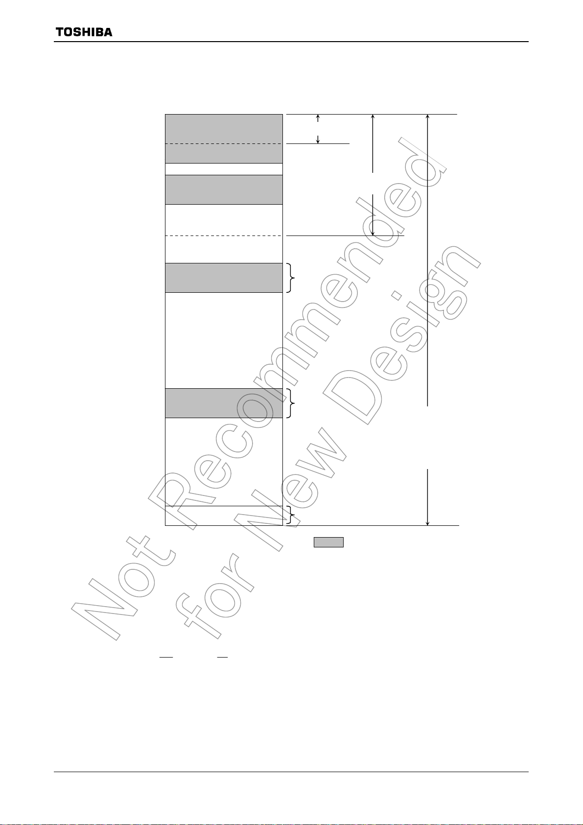
VCC (3.3 V)
RESET
High-frequency oscillation stabilized time
+20 system clock
0 s (Min)
Figure 3.1.1 Power on Reset Timing Example
92CH21-13
2009-06-19

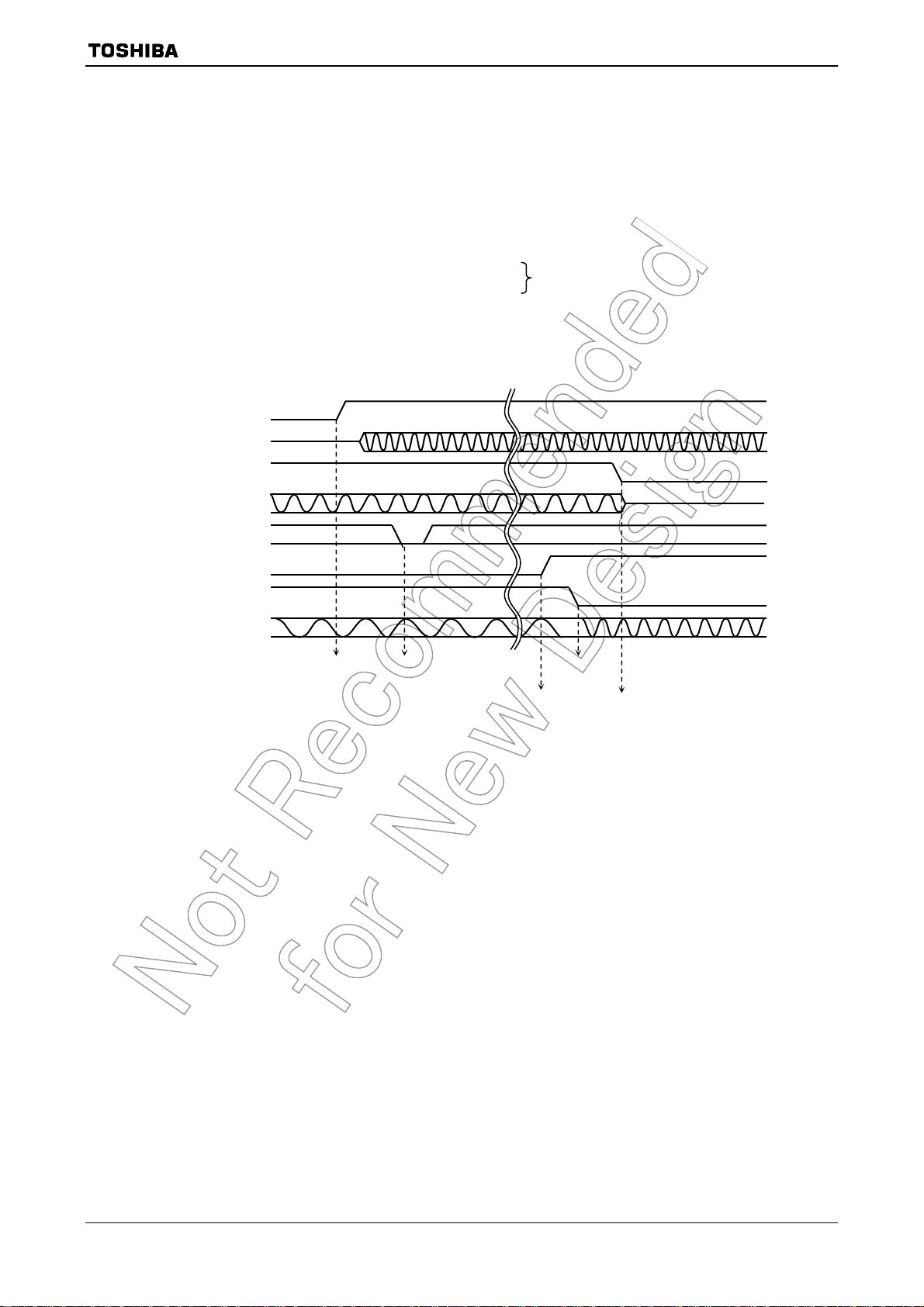
TMP92CH21
Read
Write
0FFFF00H
DATA-IN
((After reset released, starting 1
wait read cycle)
fsys×(13.5~14.5) clock
Pull up (Internal)
High-Z
Sampling
(Output mode)
(Output mode)
(Input mode)
(Input mode)
DATA-IN
DATA-OUT
32-bit external bus (AM1:0=10).
Note: This chart shows timing for a reset using a
sys
RESET
f
A23∼A0
CS2
CS0,1, 3
D0∼D31
RD
SRxxB
D0∼D31
WRxx
SRWR
PF7
SRxxB
PM1~PM2
PJ3~PJ4, PJ7
P40~P47,P50~P57
PL0~PL3
P74~P72, PK0~PK3,
PA0~PA7
P71~P72, P75~P76,
P90~P94, P96~P97,
PJ5~PJ6, PL4~PL7,
PF0~PF1, PG0~PG3,
PC0~PC3, PC6~PC7,
Figure 3.1.2 TMP92CH21 Reset Timing Chart
92CH21-14
2009-06-19
3.1.3 Setting of AM0 and AM1
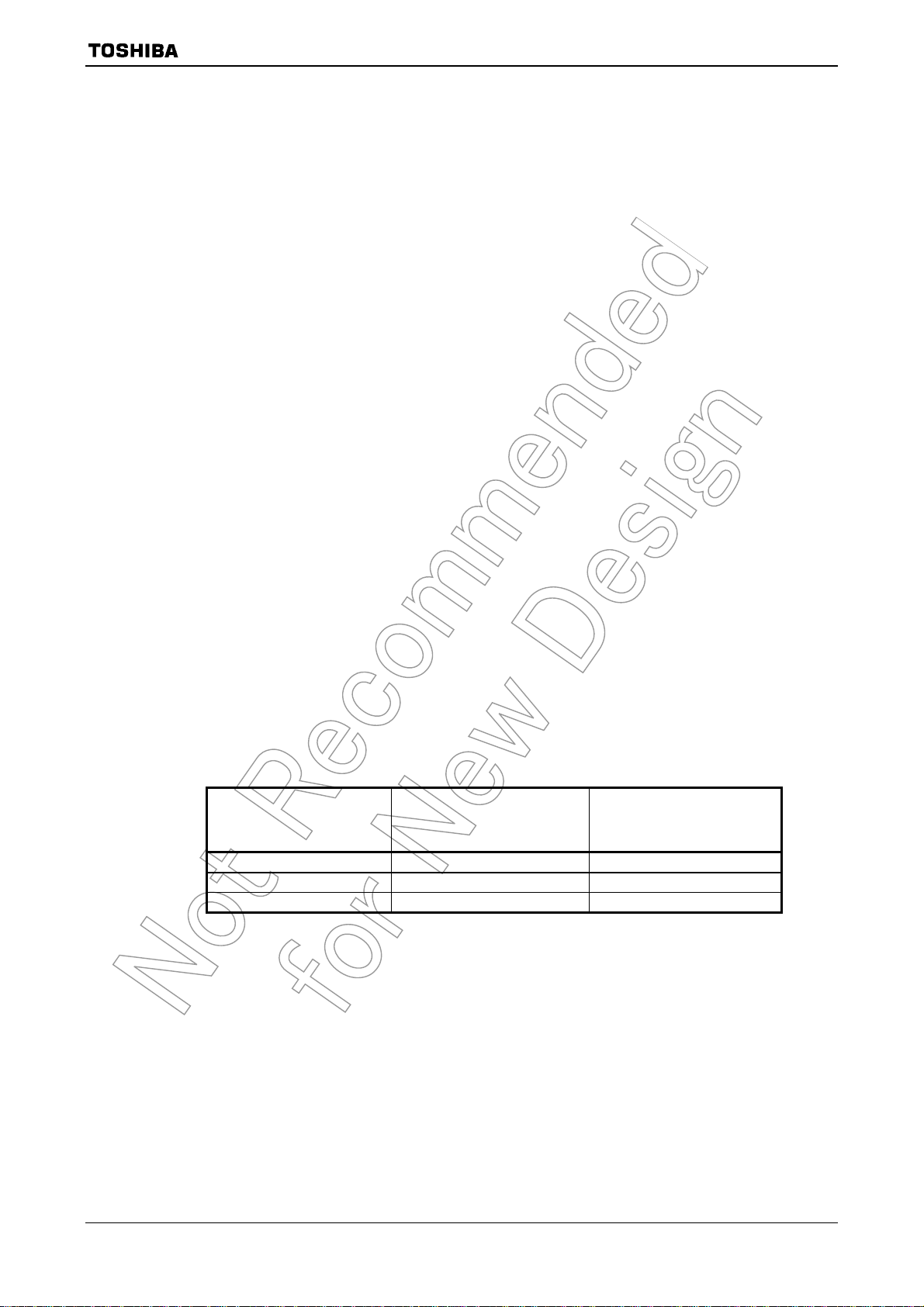
Set AM1 and AM0 pins as shown in Table 3.1.2 according to system usage.
TMP92CH21
Table 3.1.2 Operation Mode Setup Table
Operation Mode
16-bit external bus starting
(MULTI 16 mode)
32-bit external bus starting
(MULTI 32 mode)
Boot (32-bit internal MROM) starting
(BOOT mode)
Mode Setup Input Pin
RESET AM1 AM0
0 1
1 0
1 1
92CH21-15
2009-06-19
=
3.2 Memory Map
Figure 3.2.1 is a memory map of the TMP92CH21.
000000H
000100H
001D00H
002000H
006000H
Internal I/O
(8 Kbytes)
Internal RAM
(16 Kbytes)
Direct area (n)
64-Kbyte area
(nn)
TMP92CH21
010000H
3FE000H
400000H
F00000H
F10000H
FFFF00H
FFFFFFH
Boot (Internal MROM)
External memory
Provisional emulator control
External memory
Vector table (256 bytes)
(8 Kbytes)
(64 Kbytes)
(Note 1)
(Note 2)
(Note 3)
16-Mbyte area
(R)
(
−R)
+)
(R
+ R8/16)
(R
(R
+ d8/16)
(nnn)
(
Internal area)
Figure 3.2.1 Memory Map
Note 1: Boot program (Internal MROM) is mapped only for BOOT mode. For other starting modes, its area (3FE000H to 3FFFFFH)
is mapped to external-memory.
Note 2: The Provisional emulator control area, mapped F00000H to F0FFFFH after reset, is for emulator use and so is not available.
When emulator
Note 3: Do not use the last 16-byte area (FFFFF0H to FFFFFFH). This area is reserved for an emulator.
WR signal and RD signal are asserted, this area is accessed. Ensure external memory is used.
92CH21-16
2009-06-19
3.3 Clock Function and Stand-by Function
The TMP92CH21 contains (1) clock gear, (2) clock doubler (PLL), (3) stand-by controller and
(4) noise reduction circuits. They are used for low power, low noise systems.
This chapter is organized as follows:
3.3.1 Block diagram of system clock
3.3.2 SFR
3.3.3 System clock controller
3.3.4 Clock doubler (PLL)
3.3.5 Noise reduction circuits
3.3.6 Stand-by controller
TMP92CH21
92CH21-17
2009-06-19
TMP92CH21
The clock operating modes are as follows: (a) single clock mode (X1, X2 pins only), (b) dual
clock mode (X1, X2, XT1 and XT2 pins) and (c) triple clock mode (X1, X2, XT1 and XT2 pins and
PLL).
Figure 3.3.1 shows a transition figure.
Reset
(f
/32)
OSCH
IDLE2 mode
(I/O operate)
IDLE1 mode
(Operate only oscillator)
IDLE2 mode
(I/O operate)
IDLE1 mode
(Operate only oscillator)
IDLE2 mode
(I/O operate)
IDLE1 mode
(Operate only oscillator)
Instruction
Interrupt
Instruction
Interrupt
(f
OSCH
(a) Single clock mode transition figure
Instruction
Interrupt
Instruction
Interrupt
Instruction
Interrupt
NORMAL
(f
OSCH
Instruction
Instruction
Interrupt
(b) Dual clock mode transition figure
Release reset
NORMAL mode
/gear value/2)
Reset
(f
/32)
OSCH
Release reset
mode
/gear value/2)
Interrupt
SLOW mode
(fs/2)
Instruction
Interrupt
Instruction
Interrupt
Instruction
Interrupt
STOP mode
(Stops all circuits)
STOP mode
(Stops all circuits)
STOP mode
(Stops all circuits)
Reset
(f
/32)
NORMAL
(f
OSCH
OSCH
Release reset
mode
/gear value/2)
IDLE2 mode
(I/O operate)
IDLE1 mode
Instruction
Interrupt
Instruction
Interrupt
(Operate only oscillator)
Interrupt
Instruction
Instruction
Note
Instruction
Interrupt
SLOW mode
(fs/2)
Instruction
Interrupt
Instruction
Interrupt
IDLE2 mode
(I/O operate)
IDLE1 mode
(Operate only oscillator)
IDLE2 mode
(I/O operate)
IDLE1 mode
(Operate oscillator and PLL)
Instruction
Interrupt
Instruction
Interrupt
Instruction
Note
NORMAL mode
(4 × f
Using PLL
OSCH
value/2)
Instruction
STOP mode
(Stops all circuits)
/gear
(c) Triple clock mode transition figure
Note 1: It is not possible to control PLL in SLOW mode when shifting from SLOW mode to NORMAL mode with use of PLL.
(PLL start up/stop/change write to PLLCR0<PLLON>, PLLCR1<FCSEL> register)
Note 2: When shifting from NORMAL mode with use of PLL to NORMAL mode, execute the following setting in the same order.
1) Change CPU clock (PLLCR0<FCSEL>
2) Stop PLL circuit (PLLCR1<PLLON>
Note 3: It is not possible to shift from NORMAL mode with use of PLL to STOP mode directly.
NORMAL mode should be set once before shifting to STOP mode. (Sstop the high-frequency oscillator after stopping
PLL.)
← “0”)
← “0”)
Figure 3.3.1 System Clock Block Diagram
The clock frequency input from the X1 and X2 pins is called fc and the clock frequency input from the XT1 and XT2 pins is called
fs. The clock frequency selected by SYSCR1<SYSCK> is called the clock f
clock of f
, and one cycle of f
FPH
is defined as one state.
SYS
92CH21-18
. The system clock f
FPH
is defined as the divided
SYS
2009-06-19
÷2÷16÷
φ
φ
÷
3.3.1 Block Diagram of System Clock
TMP92CH21
SYSCR0<XTEN >
XT1
XT2
X1
X2
Low-frequency
oscillator
SYSCR0<XEN >
High-frequency
oscillator
f
(48 MHz) = f
USB
f
SYS
φT0
f
OSCH
f
IO
OSCH
SYSCR0<WUEF>
SYSCR2<WUPTM1:0>
Warm-up timer
(High/low-frequency oscillator)
Lock up timer
(PLL)
PLLCR1<PLLON>,
fs
Clock doubler
× 16/3
PLLCR0<LUPFG>
f
= f
PLL
OSCH
(PLL)
TMRA0 to 3,TMRB0
Prescaler
SIO0 to SIO1
Prescaler
× 4
Selector
PLLCR0<FCSEL>
USBCR1<USBCLKE>
fc
fc/2
fc/4
fc/8
4
8
Clock-gear
fc/16
SYSCR1<SYSCK>
SYSCR1<GEAR2:0>
USB
Controller
CPU
RAM, ROM
Interrupt
controller
I2S
I/O ports
f
FPH
÷2
LCDC
Memory
controller
NAND flash
controller
TSI
÷4 ÷8
÷2
fs
f
f
IO
T
T0
SYS
RTC
fs
MLD/ALM
ADC
WDT
SDRAMC
Figure 3.3.2 Block Diagram of System Clock
Table 3.3.1 Selection Example for f
High-frequency
Oscillation: f
OSCH
System Clock:
OSCH
f
SYS
(a) USB in use, with PLL 9.0 MHz 18 MHz 48 MHz
(b) USB not in use, with PLL 10.0 MHz (max) 20 MHz (max) −
(c) USB not in use, without PLL
40.0 MHz (max) 20 MHz (max) −
Note: When using USB, the high-frequency oscillator should be 9.0 MHz.
USB Clock: f
USB
92CH21-19
2009-06-19
3.3.2 SFR
SYSCR0
(10E0H)
SYSCR1
(10E1H)
SYSCR2
(10E2H)
TMP92CH21
7 6 5 4 3 2 1 0
Bit symbol XEN XTEN WUEF
Read/Write R/W R/W
Reset state 1 1 0
Function High-
frequency
oscillator
(fc)
0: Stop
1: Oscillation
Lowfrequency
oscillator
(fs)
0: Stop
1: Oscillation
Warm-up
timer
0: Write
don’t care
1: Write
start
timer
0: Read
end
warm-up
1: Read
do not end
warm-up
7 6 5 4 3 2 1 0
Bit symbol SYSCK GEAR2 GEAR1 GEAR0
Read/Write R/W R/W
Reset state 0 1 0 0
Function
Select
system clock
0: fc
1: fs
Select gear value of high-frequency (fc)
000: fc
001: fc/2
010: fc/4
011: fc/8
100: fc/16
101: (Reserved)
110: (Reserved)
111: (Reserved)
7 6 5 4 3 2 1 0
Bit symbol − WUPTM1 WUPTM0 HALTM1 HALTM0
Read/Write R/W R/W R/W R/W R/W
Reset state 0 1 0 1 1
Function Always
write “0”
Warm-up timer
00: Reserved
8
01: 2
/input frequency
14
10: 2
/input frequency
16
11: 2
/input frequency
HALT mode
00: Reserved
01: STOP mode
10: IDLE1 mode
11: IDLE2 mode
Note 1: The unassigned registers, SYSCR0<bit5:3>, SYSCR0<bit1:0>, SYSCR1<bit7:4>, and
SYSCR2<bit6, bit1:0> are read as undefined value.
Note 2: Low-frequency oscillator is enabled on reset.
Figure 3.3.3 SFR for System Clock
92CH21-20
2009-06-19
EMCCR0
(10E3H)
EMCCR1
(10E4H)
EMCCR2
(10E5H)
TMP92CH21
7 6 5 4 3 2 1 0
Bit symbol PROTECT EXTIN
Read/Write R R/W R/W R/W
Reset state 0 0 1 1
Function Protect flag
0: OFF
1: ON
Bit symbol
Read/Write
Reset state
Function
Bit symbol
Read/Write
Reset state
Function
Note: When restarting the oscillator from the stop oscillation state (e.g. restarting the oscillator in STOP mode), set
EMCCR0<DRVOSCH>, <DRVOSCL>=”1”.
Switch the protect ON/OFF by writing the following to 1st-KEY, 2nd-KEY
1st-KEY: write in sequence EMCCR1
2nd-KEY: write in sequence EMCCR1
1: External
clock
= 5AH, EMCCR2 = A5H
= A5H, EMCCR2 = 5AH
DRVOSCH DRVOSCL
fc oscillator
driver ability
1: Normal
0: Weak
fs oscillator
driver ability
1: Normal
0: Weak
Figure 3.3.4 SFR for System Clock
92CH21-21
2009-06-19
PLLCR0
(10E8H)
PLLCR1
(10E9H)
TMP92CH21
7 6 5 4 3 2 1 0
Bit symbol FCSEL LUPFG
Read/Write R/W R
Reset state 0 0
Lock up
timer
status flag
0: Not end
1: End
Function Select fc
clock
0: f
OSCH
1: f
PLL
Note: Ensure that the logic of PLLCR0<LUPFG> is different from 900/L1’s DFM.
7 6 5 4 3 2 1 0
Bit symbol PLLON
Read/Write R/W
Reset state 0
Function Control
on/off
0: OFF
1: ON
PxDR
(xxxxH)
Figure 3.3.5 SFR for PLL
7 6 5 4 3 2 1 0
Bit symbol Px7D Px6D Px5D Px4D Px3D Px2D
Read/Write R/W
Reset state 1 1 1 1 1 1 1 1
Function Output/input buffer drive-register for stand-by mode
(Purpose and use)
This register is used to set each pin status at stand-by mode.
All ports have registers of the format shown above. (“x” indicates the port name.)
For each register, refer to “3.5 Function of ports”.
Before “Halt” instruction is executed, set each register according to the expected pin-status. They will be effective
after the CPU has executed the “Halt” instruction.
This is the case regardless of stand-by mode (IDLE2, IDLE1 or STOP).
The output/input buffer control table is shown below.
OE PxnD Output Buffer Input Buffer
0 0 OFF OFF
0 1 OFF ON
1 0 OFF OFF
1 1 ON OFF
Note 1: OE denotes an output enable signal before stand-by mode.
Basically, PxCR is used as OE.
Note 2: “n” in PxnD denotes the bit number of PORTx.
Px0D
Px1D
Figure 3.3.6 SFR for Drive Register
92CH21-22
2009-06-19
3.3.3 System Clock Controller
TMP92CH21
The system clock controller generates the system clock signal (f
) for the CPU core and
SYS
internal I/O. It contains two oscillation circuits and a clock gear circuit for high-frequency
(fc) operation. The register SYSCR1<SYSCK> changes the system clock to either fc or fs,
SYSCR0<XEN> and SYSCR0<XTEN> control enabling and disabling of each oscillator,
and SYSCR1<GEAR2:0> sets the high-frequency clock gear to either 1, 2, 4, 8 or 16 (fc, fc/2,
fc/4, fc/8 or fc/16). These functions can reduce the power consumption of the equipment in
which the device is installed.
The combination of settings <XEN> = 1, <SYSCK> = 0 and <GEAR2:0> = 100 will cause
the system clock (f
For example, f
) to be set to fc/32 (fc/16 × 1/2) after reset.
SYS
is set to 1.25 MHz when the 40 MHz oscillator is connected to the X1
SYS
and X2 pins.
(1) Switching from normal mode to slow mode
When the resonator is connected to the X1 and X2 pins, or to the XT1 and XT2 pins,
the warm-up timer can be used to change the operation frequency after stable
oscillation has been attained.
The warm-up time can be selected using SYSCR2<WUPTM1:0>.
This warm-up timer can be programmed to start and stop as shown in the following
examples 1 and 2.
Table 3.3.2 shows the warm-up time.
Note 1: When
using an oscillator (other than
a resonator) with stable oscillation, a warm-up
timer is not needed.
Note 2: The warm-up timer is operated by an oscillation clock. Hence, there may be some
variation in warm-up time.
Table 3.3.2 Warm-up Times
at f
Warm-up Time
SYSCR2
<WUPTM1:0>
01 (28/frequency) 6.4 (μs) 7.8 (ms)
10 (214/frequency) 409.6 (μs) 500 (ms)
11 (216/frequency) 1.638 (ms) 2000 (ms)
Change to
Normal Mode
= 40 MHz, fs = 32.768 kHz
OSCH
Change to
Slow Mode
92CH21-23
2009-06-19

1 1 −
X
Example 1: Setting the clock
SYSCR0 EQU 10E0H
SYSCR1 EQU 10E1H
SYSCR2 EQU 10E2H
LD (SYSCR2), 0 X
SET 6, (SYSCR0) ; Enables low-frequency oscillation.
SET 2, (SYSCR0) ; Clears and starts warm-up timer.
WUP: BIT 2, (SYSCR0) ;
JR NZ, WUP ;
SET 3, (SYSCR1) ; Changes f
RES 7, (SYSCR0) ; Disables high-frequency oscillation.
X: Don’t care,
<XEN>
X1, X2 pins
<XTEN>
XT1, XT2 pins
Changing from high-frequency (fc) to low-frequency (fs).
− X
B ; Sets warm-up time to 216/fs.
Detects stopping of warm-up timer.
from fc to fs.
SYS
−: No change
TMP92CH21
Warm-up timer
End of warm-up timer
<SYSCK>
System clock f
SYS
Counts up by f
Enables
low-frequency
Counts up by fs
SYS
fc
Clears and starts
warm-up timer
Chages f
from fc to fs
End of warm-up timer
fs
Disabiles
SYS
high-frequency
92CH21-24
2009-06-19
1 0 −
X
r
r
Example 2: Setting the clock
Changing from low-frequency (fs) to high-frequency (fc).
SYSCR0 EQU 10E0H
SYSCR1 EQU 10E1H
SYSCR2 EQU 10E2H
LD (SYSCR2), 0 X
SET 7, (SYSCR0) ; Enables high-frequency oscillation.
SET 2, (SYSCR0) ; Clears and starts warm-up timer.
WUP: BIT 2, (SYSCR0) ;
JR NZ, WUP ;
RES 3, (SYSCR1) ; Changes f
RES 6, (SYSCR0) ; Disables low-frequency oscillation.
X: Don’t care,
<XEN>
X1, X2 pins
<XTEN>
XT1, XT2 pins
−: No change
− X
B ; Sets warm-up time to 214/fc.
Detects stopping of warm-up timer.
SYS
TMP92CH21
from fs to fc.
Warm-up timer
End of warm-up timer
<SYSCK>
System Clock f
SYS
Counts up by f
Enables
high-frequency
SYS
Clears and starts
warm-up time
Counts up by fc
Changes f
from fs to fc
End of warm-up
time
fcfs
SYS
Disables
low-frequency
92CH21-25
2009-06-19
TMP92CH21
(2) Clock gear controller
f
is set according to the contents of the clock gear select register
FPH
SYSCR1<GEAR2:0> to either fc, fc/2, fc/4, fc/8 or fc/16. Using the clock gear to select a
lower value of f
reduces power consumption.
FPH
Example 3: Changing to a high-frequency gear
SYSCR1 EQU 10E1H
LD (SYSCR1), XXXX0000B ; Changes f
LD (DUMMY), 00H ; Dummy instruction
X: Don’t care
SYS
to fc/2.
(High-speed clock gear changing)
To change the clock gear, write the register value to the SYSCR1<GEAR2:0>
register.It is necessary for the warm-up time to elapse before the change occurs after
writing the register value.
There is the possibility that the instruction following the clock gear changing
instruction is executed by the clock gear before changing.To execute the instruction
following the clock gear switching instruction by the clock gear after changing, input
the dummy instruction as follows (instruction to execute the write cycle).
Example:
SYSCR1 EQU 10E1H
LD (SYSCR1), XXXX0001B ; Changes f
LD (DUMMY), 00H ; Dummy instruction
Instruction to be executed after clock gear has changed
SYS
to fc/4.
92CH21-26
2009-06-19
X X X XX X
X X XX X
A
3.3.4 Clock Doubler (PLL)
TMP92CH21
PLL outputs the f
clock signal, which is four times as fast as f
PLL
OSCH
. A
low-speed-frequency oscillator can be used, even though the internal clock is
high-frequency.
A reset initializes PLL to stop status, so setting to PLLCR0, PLLCR1 register is needed
before use.
As with an oscillator, this circuit requires time to stabilize. This is called the lock up time
and it is measured by a 16-stage binary counter. Lock up time is about 1.6 ms at f
OSCH
= 10
MHz.
Note 1: Input frequency range for PLL
The input frequency range (High-frequency oscillation) for PLL is as follows:
f
= 6 to 10 MHz (VCC = 3.0 to 3.6 V)
OSCH
Note 2: PLLCR0<LUPFG>
The logic of PLLCR0<LUPFG> is different from 900/L1’s DFM.
Exercise care in determining the end of lock up time.
The following is an example of settings for PLL starting and PLL stopping.
Example 1: PLL starting
PLLCR0 EQU 10E8H
PLLCR1 EQU 10E9H
LD (PLLCR1), 1 X
LUP: BIT 5, (PLLCR0) ;
JR Z, LUP ;
LD (PLLCR0), X 1 X
X: Don’t care
B ; Enables PLL operation and starts lock up.
Detects end of lock up.
B ; Changes fc from 10 MHz to 40 MHz.
<PLLON>
<FCSEL>
PLL output: f
Lock up timer
<LUPFG>
System clock f
PLL
SYS
Counts up by f
During lock up
Starts PLL operation and
starts lock up
OSCH
fter lock up
Changes from 10 MHz to 40 MHz
Lock up ends
92CH21-27
2009-06-19
X: Don’t care
Example 2: PLL stopping
PLLCR0 EQU 10E8H
PLLCR1 EQU 10E9H
LD (PLLCR0), X0XXXXXXB ; Changes fc from 40 MHz to10 MHz.
LD (PLLCR1), 0XXXXXXXB ; Stop PLL.
<FCSEL>
<PLLON>
TMP92CH21
PLL output: f
System clock f
PLL
SYS
Changes from 40 MHz to 10 MHz
Stops PLL operation
92CH21-28
2009-06-19
 Loading...