


NETWORK EXPANSION KIT
GA-1170
File No. SME04003700
R04122173800-TTEC
Ver00_2005-02

© 2005 TOSHIBA TEC CORPORATION
All rights reserved
Parts marked with “ ” are important for maintaining the safely of the machine. Be sure to replace these
parts with the replacement parts specified to maintain the safety and performance of the machine.

General Precautions for Installation/Servicing/Maintenance for the GA-1170
The installation and service should be done by a qualified service technician.
1. When installing the GA-1170 to the Equipment, be sure to follow the instructions
described in the "Unpacking/Set-Up Procedure for the GA-1170" booklet which comes
with each unit of the GA-1170.
2. The GA-1170 should be installed by an authorized/qualified person.
3. Before starting installation, servicing or maintenance work, be sure to turn OFF and
unplug the equipment first.
4. When servicing or maintaining the GA-1170, be careful about the rotating or operation
sections such as gears, pulleys, sprockets, cams, belts, etc.
5. When parts are disassembled, reassembly is basically the reverse of disassembly
unless otherwise noted in this manual or other related materials. Be careful not to
reassemble small parts such as screws, washers, pins, E-rings, toothed washers to the
wrong places.
6. Basically, the machine should not be operated with any parts removed or disassembled.
7. Delicate parts for preventing safety hazard problems (such as switches, sensors, etc. if
any) should be handled/installed/adjusted correctly.
8. Use suitable measuring instruments and tools.
9. During servicing or maintenance work, be sure to check the serial No. plate and other
cautionary labels (if any) to see if they are clean and firmly fixed. If not, take appropriate
actions.
10. The PC board must be stored in an anti-electrostatic bag and handled carefully using a
wristband, because the ICs on it may be damaged due to static electricity. Before using
the wrist band, pull out the power cord plug of the equipment and make sure that there
is no uninsulated charged objects in the vicinity.
11. For the recovery and disposal of used GA-1170, consumable parts and packing
materials, it is recommended that the relevant local regulations/rules should be
followed.
12. After completing installation, servicing and maintenance of the GA-1170, return the
GA-1170 to its original state, and check operation.

CONTENTS
[ 1 ] CONFIGURATION ................................................................................ 1 - 1
[ 2 ] SPECIFICATIONS................................................................................. 1 - 1
[ 3 ] UNPACKING AND INSTALLATION ....................................................... 3 - 1
[ 4 ] SETUP IN A WINDOWS ENVIRONMENT ............................................ 4 - 1
[ 5 ] UPDATING NETWORK BOX FIRMWARE............................................ 5 - 1
[ 6 ] TROUBLE CODE .................................................................................. 6 - 1
[ 7 ] CIRCUIT DIAGRAM .............................................................................. 7 - 1
[ 8 ] PWB PARTS LAYOUT .......................................................................... 8 - 1
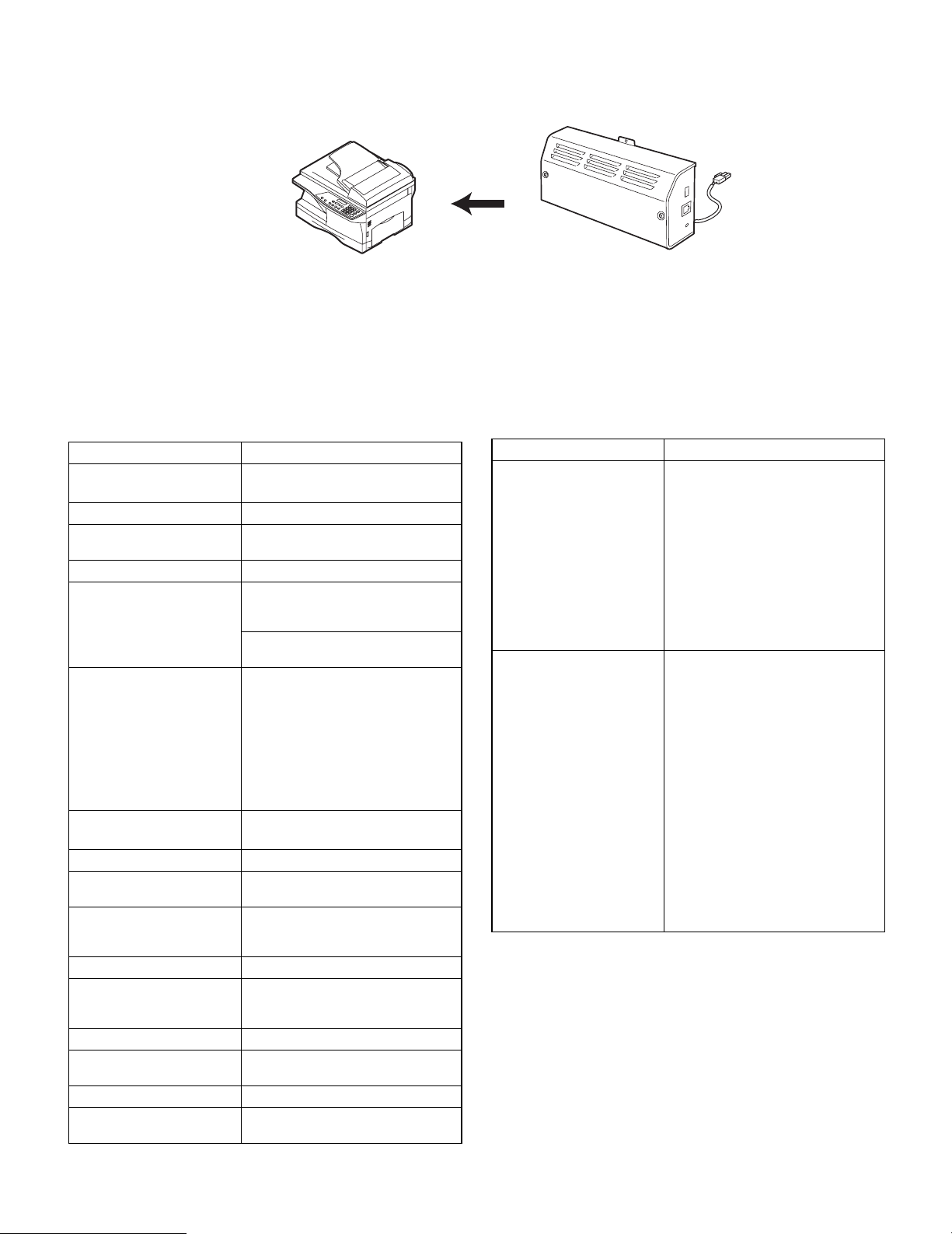
[ 1 ] CONFIGURATION
e-STUDIO162/162D
e-STUDIO151/151D
[ 2 ] SPECIFICATIONS
1. BASIC SPECIFICATIONS
ITEMS SPEC
Extensible model e-STUDIO162/162D
e-STUDIO151/151D
Standard memory 64MB
Expansion memory DIMM 1slot
Platform of Client PC IBM PC/AT compatible, Macintosh
Useable OS W i n dows98/Me /N T 4 . 0 / 2 0 0 0
Required hardware(PC)
Required software Internet Explorer 5.5 or later
Extensible option PS extensible kit (GA-1180)
Network Protocol TCP/IP, IPX/SPX, NetBEUI, Ether
Emulation (The functions
which can be used differ by
The MFP connected)
Network Print PCL/PS
Network Scan (The functions
which can be used differ by
The MFP connected)
E-mail alert status Yes (Cancels by the soft key)
Power supply Supplies via copier
Power consumption 5.5W
Outside dimension
(W x D x H)
144pin 128/256MB SO-DIMM
professional/Windows XP Home
Edition/Professional Edition
Mac OS 8.6-9.x,10.1.5,10.2-10.2.8(w/
o 10.2.2)(PS option)
(System)
The conditions of each OS which can
be used are required.
(HDD)
Exceeding 100M is recommended.
(Monitor)
800 x 600 dots
(Interface)
10BASE-T/100BASE-TX Ethernet
Netscape Navigator 6 or later
Talk
PCL/PS (PS:Cancels by the soft key)
Scan to E-mail, Scan to FTP,
Scan to Desktop
(AC power supply built-in) AC120mA
248mm x 127mm x 59mm
GA-1170
ITEMS SPEC
Accessories USB cord x 1
(for connection to Copier)
Software CD-ROM x 3
Screw for installation x1
Clamp x 1
(for harness fixation)
Installation manual
Installation guide
*An installation manual exists in
driver CD-ROM by the pdf file format.
Bundle software Disk1:Driver CD-ROM
for e-STUDIO162/162D,
e-STUDIO151/151D
• PCL driver (Win)
• PS driver (Win/Mac)
• SMON (Win)
• PAU (Win)
• NIC Manager (Win)
• Online manual (Win/Mac)
Disk2:Network setting CD-ROM
• NIC Manager (Win)
• Quick Setup (Win)
• SC-Print2000 (Win)
• Online manual (Win/Mac)
• Setup Utility (Mac)
Disk3:Application CD-ROM
• Desktop Document Manager
(3 license)
GA-1170 CONFIGURATION
1 – 1
2. FUNCTION DESCRIPTION
A. PRINT EMULATION
A difference exists in the function which can be used by execution of the basic performance and composition of the MFP to connect (print size/configuration).
(1) comparison table of main print function classified by driver
Function
General Document
Style
Booklet Yes No
Binding Edge No
N-up
N-up Order Z Z, Reverse Z, N, Reverse N Z
Custom
Paper Size
Different 1st
(Cover)
Graphic Resolution
Setting
Half tone
Setting
Graphics
Mode
Negative
Image
Mirror Image No Yes
Fit to Page Yes
Font Resident
Font 80 fonts
Download font
Others Configura-
tion Setting
Job
Compression
Bitmap
Compression
PCL5e
Custom Driver
1-Sided, 2-Sided(Book) 2-Sided(Tablet), Pamphlet Style(Tiled Pam-
phlet), Pamphlet Style(2-up Pamphlet)
600/300 dpi 600dpi
Raster/HP-GL2 Raster/Vector No
PCL6 (XL)/
SPDL2
Custom Driver
2/4/6/8/16
1size 3 sizes
Yes No
No Yes No
No Yes
Yes No Yes
Yes (Automatic) No
No Yes No
No Yes No
PS
Custom Driver
1-Sided, 2-Sided(Book), 2-Sided(Tablet)
136 fonts,
5 Kanji fonts
(Japan only)
Macintosh
PPD file
35 fonts,
5 Kanji fonts
(Japan only)
Windows
PPD file
Win 9x : 2/4
Win2K/XP: 2/4/6/8/16
X
136 fonts,
5 Kanji fonts
(Japan only)
(2) comparison table of printing function for each driver
The model to connect e-STUDIO162/162D, e-STUDIO151/151D
Function PCL5e PCL6 PS Mac PPD Win PPD
General Copies 1-999
Orientation Portrait/Landscape
Collate Collate/Group
Document Style 1-Sided, 2-Sided(Book), 2-Sided(Tablet),
Pamphlet Style(Tiled Pamphlet), Pamphlet Style(2-up Pamphlet)
Booklet (e-STUDIO162/162D, e-STUDIO151/151D)
Invoice on Letter, A5 on A4, Letter on Letter, A4 on A4
Binding Edge No
Margin Shift No
N-up 2/4/6/8/16
N-up order Z Z, Reverse Z, N, Reverse N Z
GA-1170 SPECIFI CATIONS
1 – 2
1-Sided, 2-Sided(Book), 2-Sided(Tablet)
No
Win9x: 2/4
Win2k/XP: 2/4/6/8/16
*2

The model to connect e-STUDIO162/162D, e-STUDIO151/151D
Function PCL5e PCL6 PS Mac PPD Win PPD
General N-up Border On/Off Yes
On/Off
*2
(Single hairline/Single thin line/Double
hairline/Double thin
line)
Paper Paper Size (e-STUDIO162/162D, e-STUDIO151/151D)
A3/B4/A4/B5/A5/B6/A6/11x17/8.5x14/8.5x13/8.5x11/5.5x8.5/Folio/Executive/COM-10/Monarch/DL/C5/8K/16K
Fit to Page size (e-STUDIO162/162D, e-STUDIO151/151D)
A4/B5/A5/B6/A6/8.5x14/8.5x13/8.5x11/5.5x8.5/Folio/Executive/COM-10/Monarch/DL/C5/8K/16K
Paper Type No
Custom Paper
1 size 1size
*1
3 sizes
Size
Source Selection Auto/Bypass (Auto)
e-STUDIO162/162D, e-STUDIO151/151D: Tray 1/2
Different 1st
On/Off No
(cover)
Transparency
No
Inserts
Carbon Copy No
Paper
Output
Output Tray
Selection
No
Staple No
Graphic Resolution Setting 600/300 dpi 600 dpi
Half tone Setting No
Graphics Mode Raster
HP-GL2
Raster
Vector
Screen Frequency 8 to
360.0 in 0.1 steps
Screen angle 0.0 to
360.0 in 0.1 steps
No
No
Smoothing No
Toner save No
Half tone Enhance No
Graphic
Brightness No
Negative Image No On/Off
Mirror Image No Horizontal/Vertical
Zoom No 25-400%
Fit to Page On/Off No
Font Resident Font 80 fonts 136 fonts 35 fonts 136 fonts
Download Font
Others Configuration Set-
Bitmap, TrueType, Graphics
No
Yes (Automatic) No
Type1
True Type
ting
ROPM On/Off
Overlay On/Off No
Print Auditor No
Job Retention No
Watermark On/Off On/Off(With functional restriction)
Page Protection No
Job Compression No
Job Compression No
None, Fastest, Fast,
Medium, Best
None, Very High, High,
Medium, Draft
No
No
*1:Mac OS 10.1 is not supported.
*2:Windows NT is not supported.
*2
GA-1170 SPECIFI CATIONS
1 – 3
(3) PDF/TIFF direct printing function
PDF and TIFF files can be specified from a web page and directly
printed out.
(4) Limitations (printing function)
If a print request for GDI/SPLC data is made, an error message is
printed out.
(5) Printer condition setup
The following setup can be made from the web page.
Default Setting Items
Item
Function
e-STUDIO162/162D,
e-STUDIO151/151D
Default
Copies 1-999 1
Orientation Portrait / Landscape Portrait
Default Paper Size (Overseas)
Invoice
•
Letter
•
Foolscap
•
Legal
•
Letter or A4
(Domestic)
A5 •B5
•
A4
•
(China - size of AB system)
A5 •B5 •A4
•
16K
•
Default Paper Source drop down box select
AUTO
values:
AUTO •Tray1
•
Tray2
•
BYPASS
•
Disable Blank Page Print
Enable/Disable Disable
*When destination lan-
guage is Japanese.
2-Sided Print dr o p do wn b o x sl ect
1-SIDED
values:
1-SIDED
•
2-SIDED (BOOK)
•
2-SIDED (TABLET)
•
ROPM Enable / Disable Disable
(6) Network status page
The network status pages shows a list of settings about the network.
Data are printed out in the A4 or letter size in US English regardless of
the destination and OS language selected.
The status page can be printed out by pressing the status switch on the
network expansion kit.
Note:
1. The name of the printer is printed under the item "printer name."
2. When WINS is disabled, "WINS server 1-5" is not displayed. It is
displayed when a value is set or information is acquired from the
DHCP server.
Any server which responds normally to the registration of WINS is
marked with an asterisk "
"WINS server" shows up to 5 values: 2 settings, 2 DHCP values,
and broadcast. However, the broadcast operates only when no normal response is returned from any server.
3. The "WINS Scope ID" is displayed only when a value is set or when
information is acquired from the DHCP server and more than one
piece of information is valid as a WINS server.
".
∗
B. NETWORK SCANNING FUNCTION
It is possible to use the MFP scanning function as a network scanner
with a network scanner expansion kit. Setups can be made using a
Web browser. Supported functions vary with the type of the MFP connected.
(1) Basic scanning function
Function Item
Network
scanner
Scan to E-mail Yes
Scan to Desktop
Scan to FTP
server
Destination
Specify e-mail
address with
LDAP
AdHoc
(Enter e-mail
address from
MFP.)
File
format
JPEG
PDF
(non-compression, G3, G4)
TIFF
(non-compression,G4, G4)
(2) Scanner settings
Item Default
Setting
Scanning size
File
format
Color
mode
Resolution
B/W
threshold
e-STUDIO162/162D,
e-STUDIO151/151D
JPEG color/JPEG
gray scale/PDF
color/PDF gray
scale/PDF monochrome,
binary non-compression/PDF
monochrome,
binary G3 compression/PDF
monochrome,
binary G4 compression/TIFF
color/TIFF gray
scale/TIFF monochrome,
binary non-compression/TIFF
monochrome,
binary G3 compression/TIFF
monochrome,
binary G4 compression
Monochrome,
2 gradations/Gray
scale/Full color
75/100/150/200/
300/400/600
1-254
(default: 128)
e-STUDIO162/162D,
e-STUDIO151/151D
Remarks
Yes
Yes
Yes
Yes
Yes
e-STUDIO162/162D,
e-STUDIO151/151D
TIFF/PDF multiple page support
Remarks
A4 (AB region)
Letter (Inch-sys-
tem region)
TIFF monochrome,
binary G4 compression
Monochrome,
2 gradations
Available only at
the “monochrome”.
75 Selectable reso-
lutions vary with
different memory capacities.
128
GA-1170 SPECIFI CATIONS
1 – 4

Item Default
Setting
Light
source
e-STUDIO162/162D,
e-STUDIO151/151D
Red/
Green/
Blue
White/
Red/
Green/
Blue
e-STUDIO162/162D,
e-STUDIO151/151D
Green White Light source can
Remarks
be selected only
when the color
mode is in
"Monochrome".
Void On/Off On When On is
selected, the
edges of images
are cut.
(3) Send file (message and filename)
• Information contained in filename
Sender name : Use MFP product name.
Date & Time : Date and time at which file is sent
Session page
counter
Unique identifier : Automatically created based on the information
Example:
e-STUDIO162D_20000620_155114_0057_06a3f3393948.pdf
• Mail subject
Can be freely set.
Default: Scanned image. device name: e-STUDIOXXX (MFP product
name)
Example: Scanned image. device name: e-STUDIO162D
• Mail message
The following messages are added to the image send mail.
: Image send counter
of the date and time and image send counter.
(4) Recipient registration
[e-STUDIO162/162D, e-STUDIO151/151D]
• Up to 200 destinations can be registered on the network expansion
kit to which the scan can be sent from the network scanner.
• The mail address registered for each destination can be selected
from the mail address which is searched using LDAP.
• The information for each recipient includes the recipient name, IP
address or mail address, scanning size, format type, and scan
parameter.
• Either of LDAP-selected or directly-entered mail address scan setting
is available. If the destination is a mail address entered through the
main system or selected by LDAP, this scan setting is used.
• The destination name is displayed on the LCD.
(5) Scanning size
[e-STUDIO162/162D, e-STUDIO151/151D]
• Scanning size is the size set up in main unit(Copier).
(Apply to the main scan, a subscan, ADF, and OC)
(6) Scanner limitations
[e-STUDIO162/162D, e-STUDIO151/151D]
• The scanning function is allocated to the network expansion kit. The b
Button Manager settings are disabled.
• When the network expansion kit is connected, the scanner function
through TWAIN (pull scan) and push scan which used button manager on pc are not available.
Device name: Freely set
Model: MFP product name
Location: Freely set
File type: File type of send image
Resolution: Resolution of send image
Example;
Device name :e-STUDIO162D
Model name :e-STUDIO162D
Location :D2) Planning dept.
File type :PDF MMR (G4)
Resolution :200 dpi x 200 dpi
GA-1170 SPECIFI CATIONS
1 – 5

C. FUNCTIONS BY INTERFACE
When the network expansion kit is connected, the following functions
are available by system interface.
System I/F
(main unit)
USB2.0 RJ45 (LAN) No No Yes Yes Yes
USB1.1
IEEE1284
USB2.0
USB1.1 RJ45 (LAN) No No Yes (*2) Yes (*2) No
IEEE1284
USB1.1 RJ45 (LAN) No No Yes (*2) Yes (*2) No
IEEE1284
(*1): PS requires soft keys of the GA-1180.
(*2): Some functions are not available.
GA-1170 I/F
➝
➝
➝
➝
➝
SPLC GDI PCL5e/6 PS (*1) Net
Yes No No No No
Yes No No No No
Yes No No No No
Yes No No No No
No Yes No No No
Function
Scan
D. NETWORK SETUP
Network setups should be performed by the system administrator. Use
a setup tool such as TCP/IP, Netware, Ether Talk or Web interface.
E. SOFTWARE SETUP
The network expansion kit can be installed by setting up NIC, installing
a printer driver with the total installer, and installing Desktop Document
Manager.
(1) Installing driver
The network expansion kit printer is connected only through the network. The port setup required for installing a printer driver is the network
only. The following items should be set up.
• TCP/IP peer-to-peer port
1) Search for the network expansion kit on the network and select the
network expansion kit you want or enter the IP address of the applicable network expansion kit to create a TCP/IP port.
2) Install the driver to the created port.
• Windows printer shared port
When the setup of the above client PC is completed and the printer is
set to "Windows shared printer," other client PCs can select this
printer shared port and then proceed to installation of the driver.
F. HARDWARE SETUP
Supplied by the main unit
[e-STUDIO162/162D, e-STUDIO151/151D]
1) Connection to the system unit
• Connect to the USB2.0 port
2) Power supply
Supplied by the main unit.
GA-1170 SPECIFI CATIONS
1 – 6
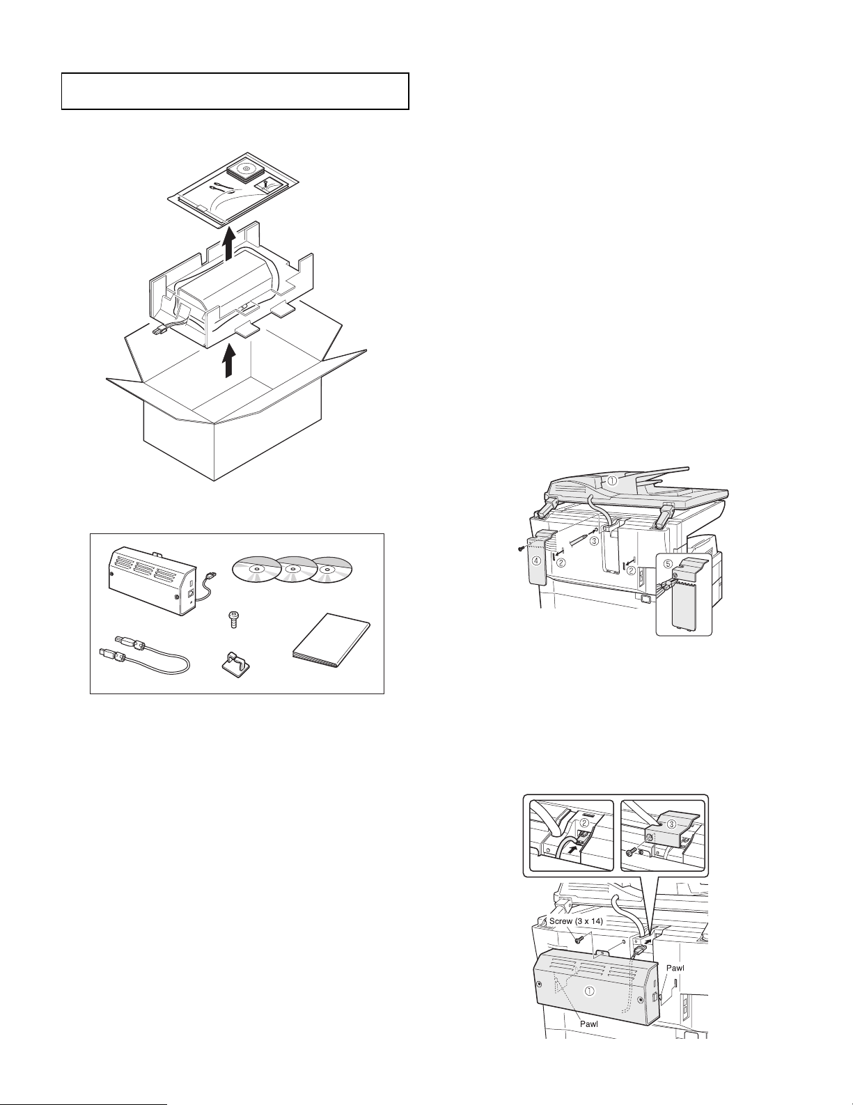
[ 3 ] UNPACKING AND INSTALLATION
The unpacking and set-up procedure shall be done by a qualified
service technician.
1. UNPACKING
2. PACKAGED GOODS
Parts included
3. INSTALLATION PROCEDURE
This installation procedure is provided for e-STUDIO162/162D,
e-STUDIO151/151D.
For Installation to other models, see the operation manual of the main
unit or the service manual.
Turn off the main switch of the main unit and remove the power
plug of the copier from the outlet.
1. Cut the rear cabinet.
1) Remove the ADF/ RADF from the main unit and gently place it on
the document glass as shown in the illustration.
2) Cut out two cut-out portions from the rear cabinet using a cutter or
the like.
3) Use a Phillips screwdriver or the like to open a hole.
4) Remove the screw and then remove the rear cabinet cover.
5) Cut out a part of the rear cabinet cover with nippers or the like as
shown in illustration.
(Be careful about the orientation of the nippers so that the cross
section is flat.)
Network
expansion kit
USB cable ... 1 pc.
CD-ROM ... 3 pcs.
Screw (3 x 14) ... 1 pc.
Clamp ... 1 pc.
Important
information ... 1 sheet
2. Attach the network expansion kit.
1) Engage the two pawls on the rear of the network expansion kit with
the cutout portions of the main unit and secure the kit with the supplied screw (3 x 14).
2) Connect the connector of the network expansion kit to the connector of the main unit.
3) Secure the rear cabinet cover to the main unit with the screw.
4) Attach the ADF/ RADF to the main unit.
GA-1170 UNPACKING AND INSTALLATION
3 – 1
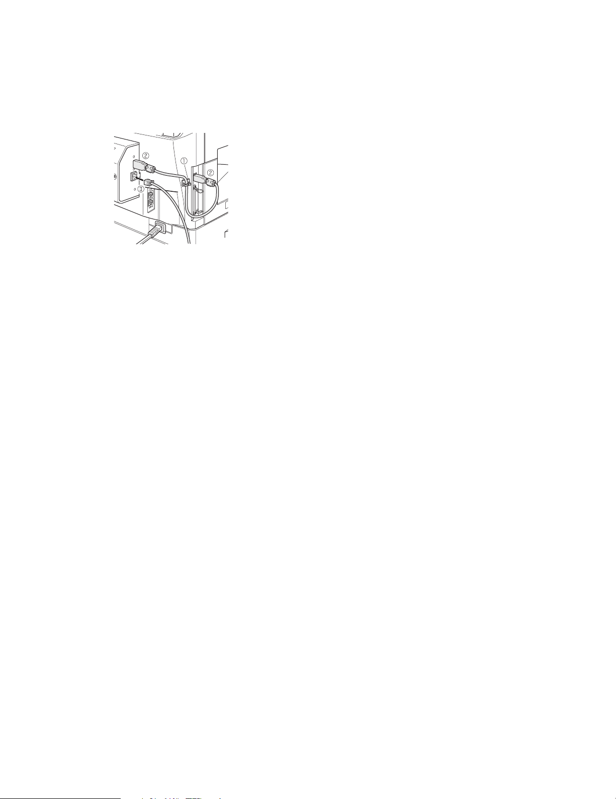
3. Connect the USB cable and the network cable.
1) Attach the supplied cable clamp to the position shown in the illustration.
2) Connect the USB cable to the network expansion kit and the main
unit.
At this time, reduce slack of the cable with the cable clamp as
shown in the illustration.
3) Connect the network cable.
Insert the power plug of the copier to the outlet, turn the main
switch of the copier to the “ON” position, and then perform network setting and installation of the software.
GA-1170 UN PACKING AND INSTALLATION
3 – 2

[ 4 ] SETUP IN A WINDOWS ENVIRONMENT
1. SETTING THE IP ADDRESS OF THE
MACHINE
Before installing the printer driver, be sure to set the IP address of the
machine. Consult your network administrator for the correct IP address,
subnet mask, and default gateway to be entered. If a DHCP server will
automatically assign an IP address to the machine, the following procedure is not necessary. (To check the IP address assigned to the
machine by DHCP, see "2. CHECKING THE IP ADDRESS" .)
Note: If the machine is used in a DHCP environment, the machine's IP
address may change automatically. If this happens, printing will
no longer be possible. In this event, use a WINS server or do not
use the machine in a DHCP environment.
1) Make sure that the LAN cable is connected to the machine and then
turn on the machine.
2) Insert the network expansion kit GA-1170 "Software" CD-ROM into
your computer's CD-ROM drive.
3) Click the "start" button, click "My Computer" ( ), and then doubleclick the CD-ROM icon ( ).
In Windows 95/98/Me/NT 4.0/2000, double-click "My Computer"
and then double-click the CD-ROM icon.
4) Double-click the "setup" icon ( ).
Note: If the language selection screen appears after you double click
the "setup" icon, select the language that you wish to use and
click the "Next" button. (Normally the correct language is
selected automatically.)
5) The "SOFTWARE LICENSE" window will appear. Make sure that
you understand the contents of the license agreement, and then
click the "Yes" button.
6) Read the message in the "Welcome" window and then click the
"Next" button.
7) Click the "Administrator Tools" button.
8) Click the "NICManager" button.
9) The printer or printers connected to the network will be detected.
Click the printer to be configured (the machine).
Select the "GA-1170".
10) Click the "Print Server Card Setup" button.
Enter your password in the password entry screen and click "OK".
The Print Server Card Setup window will appear.
The password for this product has been initially set to "TOSHIBA".
If the "Guest user" checkbox is selected, the settings can be
viewed but not configured.
11) Click the "TCP/IP" tab.
GA-1170 SETUP IN A WINDOWS ENVIRONMENT
4 – 1

12) Configure the settings and then click the "Update" button.
Be sure to ask your network administrator for the correct IP
address, subnet mask, and default gateway to be entered.
13) Your changes to the settings appear.
Make sure that the changes are correct and then click the "OK"
button.
14) Restart the machine.
Power off the machine and then power it back on.
15) Select "Search" from the "File" menu.
The IP address that you entered will appear. Make sure that it is
correct.
The completes the IP address settings.
3. PRODUCT KEY SETTING
To enable the PS3 function and the e-mail status & alerts function,
follow the procedures below. In addition, to enable the PS3 function,
you need GA-1180 (option).
1) Make sure that the LAN cable is connected to the machine and then
turn on the machine.
2) Enter the IP address in web browser to open the web page.
3) Select "Product Key Setting" in "Device Setup" from MENU.
4) Set "User name" to "admin" and "Password" to "TOSHIBA" in the
screen displayed.
5) Click the "OK" button to obtain the "Product Number".
2. CHECKING THE IP ADDRESS
To check the IP address of the machine, press the status button on the
network expansion kit to print out a network status page.
6) Fill in the product number in the following column of the product
sheet (MACHINE SERIAL NUMBER).
APPLICATION NUMBER
MACHINE SERIAL NUMBER
PRODUCT KEY
XXXXXXXXX
7) Obtain the product key with APPLICATION NUMBER and
MACHINE SERIAL NUMBER in the product sheet.
For specific procedure to obtain the product key, contact the
TOSHIBA authorized dealer.
In addition, keep the product sheet after filling in since the product
key is important information.
8) Enter the product key in the web page displayed in 5), and click the
"Submit" button.
This completes the PS3 setting.
9) Select "E-mail status & alerts" from the "Option Name" list in the
"Product Key Setting" screen.
10) Click the "Submit" button.
This completes the e-mail status & alerts function setting.
GA-1170 SETUP IN A WINDOWS ENVIRONMENT
4 – 2

[ 5 ] Updating Network Box Firmware
Update the Network Box firmware in the following procedure using a
Web browser.
1. Display the web page for updating Network Box firmware
Start the browser on your PC and specify the following URL. A web
page, as shown in Fig. 1, appears on screen.
http://<IP Address of Network Box>/firmware_upload.html
[Fig.1: Web page for updating Network Box firmware]
2. Switch to firmware upload mode
Click the button on the screen, the message shown in Fig. 2
appears.
The page changes to the Network Box firmware upload mode.
The browser is automatically reloaded and then the screen looks
like this.
*When the screen shown in fig.3 is not displayed, refresh a browser
manually.
[Fig. 3: Upload mode]
3. Specifying the file
Click the Browse button. Selects the firmware of the Network Box
version you want to update, from the file selection menu indicated in
Fig.4.
[Fig.2: Switch to firmware upload mode]
[Fig. 4: Specifying the file]
Note: If you want to set the IP address of the Network Box at first, use
the NIC Manager. Select and set your model name and an
appropriate Ethernet address from the list.
Both the Boot and Main files can be updated in the same procedure as mentioned above. However, when you want to update
both at the same time, you need to update them separately by
repeating the same procedure twice.
When updating both files, it is required to first update Boot and
then Main.
GA-1170 Updating Network Box F irmware
5 – 1

4. Updating the firmware
After you select the file, click the Submit button. The firmware is
transmitted to Network Box, and it is updated. The message indicated in Fig.5 blinks repeatedly until the updating process is completed. Do not turn off the power supply.
[Fig.5: Updating in progress]
5. Restarting your MFP
When updating is completed, the message shown in Fig.6 appears
on screen. Turn off the power and then turn it on again to restart
Network Box.
Caution: If a DHCP is used, the browser may not be able to reload auto-
matically in some cases when transferring to the upload mode
because different IP addresses are read. Therefore, we recommend that you use a fixed IP address when updating firmware.
If the upload mode is operating with different IP addresses,
check the IP address obtained by the Ethernet address of Network Box from the DHCP server and display the updating
mode URL again using the browser.
When a proxy server is used, the screen may not be updated
by reloading. In that case, you need to update manually.
[Fig.6: Updating completed]
GA-1170 Updating Network Box F irmware
5 – 2

[ 6 ] TROUBLE CODE
1. TROUBLE CODE (CE CODE)
If "CE" blinks in the display, press the [START] key. An error code will
appear.(Only e-STUDIO162/162D, e-STUDIO151/151D displays an error
code automatically.) Solve the problem as explained below.
Error Code Solution
CE-00 Error which cannot be specified occurred.
Turn off the power and turn it back on. Consult with
your network administrator to make sure that no problems exist on the network or in the server.
CE-01 Network Server card error.
Turn off the power and turn it back on. Consult with
your network administrator to make sure that no problems exist on the network or in the server.
CE-02 Server access denied. The scanned image was not
CE-03 The scanned image was not sent because the server
CE-04 It has not logged in to the FTP server and the mail
CE-05 The scanned image was not sent because the directory
CE-09 The size of the scanned image file exceeds the upper
CE-10 A transmission method assigned to a [SCAN MENU]
CE-11 The memory filled with scanner data.
CE-12 The quantity of the result for which LDAP searched
sent because a connection to the server could not be
established. Make sure that the SMTP server settings
or FTP server settings in the Web page are correct.
was busy or there was too much traffic. Wait briefly and
then try again.
server. Please reconfirm the login name and a password.
of the destination FTP server was not correct. Make
sure that the correct FTP server information is configured in the Web page.
limit set in "Maximum Size of File" in the Web page.
Reduce the number of original pages scanned into the
file, or change the upper limit set in "Maximum Size of
File".
key cannot be used. Check the transmission methods
assigned to the [SCAN MENU] keys in "Enable Scanner Delivery to:" in the Web page whether or not the
method can be used.
It was not able to process by the size of a scanner data
being too large.
Please drop resolution of data by setup of scaner and
retry scan.
exceeded the maximum quantity which can be
searched.
There are too many addresses which were in agreement with reference conditions.
Please increase the number of reference characters
and perform re-reference.
GA-1170 TROUBLE CODE
6 – 1

B
D
D
C
C
B
A
1/16
12345678
1
1
SPD
MEMD[63:0]
2
345678
On Board 64MB
256MB(Max)
SDRAM1 SO_DIMM
256Mbit
SDRAM0(H)
256Mbit
SDRAM0(L)
100MHz/64bit
System BUS
MEMA[14:5]
ADDR[19:0]
MEMD[31:16]
MEMD[15:0]
DATA[63:0]
32.768KHz
256Kbit
Serial EEPROM
HC125
RTC
LCX125
MEMD[31:0]
BUSSPRT
LCX245
LCX244
ACE
slot2 32MB
ROM)
Flash SO-DIMM (Mask
slot1 8MB
SO-DIMM
Flash
slot0 12MB or 16MB
SO-DIMM
Flash
3.3V
LCH
LCX373
LD[31:0]
LD[31:0]
LA[20:0]
LD[31:0]
2
3
3
Tx49Core
CPUCLK = 200MHz
TMPR4927TB
OSC
25MHz
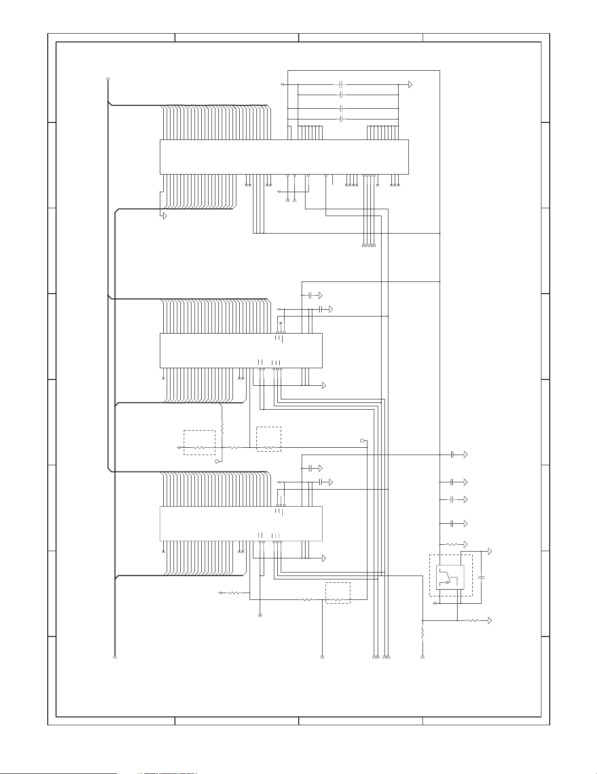
[ 7 ] CIRCUIT DIAGRAM
1. BLOCK DIAGRAM
D
D
SDRAMC
PCI BUS
33MHz/32bit
EBIF
Connector
PCI
G-Bus
PCIC
EBUSC
C
C
Bridge
PIO
IM-Bus
12MHz
(MAC/PHY)
DP83816
Connector
Ethernet
ISP1561
USB2.0
Connector
USB
IRCUART
B
B
UART Ch1
LCX14
4Pin Connector
(RS-232C Connector)
A A
A
87654
87654
GA-1170 CIRCUIT DIAGRAM
7 – 1

B
D
D
C
C
B
A
2/16
12345678
1
113355779
2244668810
CN11
<JTAG CONNECTOR>
2
345678
VCCIO
NOASM
R250 1K
R249 1K
R248 1K
R247 1K
TP714
TP712 TP713
TP711
TP710
R289 33
9
RF-H102TD-1130
NOASM
10
R291 33
R292 33
R293 33
R290 33
RTCDATA 8,16
DIMM_SCK 5,16
EEP_SCK 8,16
RTCR/W 8,16
DIMM_SDA 5,16
RTCCS 8,16
PIO_SW 13,16
VCCWCTL 7,16
RTCCLK 8,16
EEP_SDA 8,16
HDD_POWER 9
DBG_LED1 13,16
DBG_LED3 13,16
DBG_LED0 13,16
DBG_LED2 13,16
1
2
3
3
TP738
TP736
TP737
TP639
B13
TPCO/TDO
TX4927/TX4837 1/5
TDI/DINT
IC1A
C11
B11
B12
TCK
TP742
DCLK
TMS
C12
E16
TP743
TP744
A17
C16
B16
PCST0
PCST1
TRST
RESET
K1
PONRST7,9,10,11,13,15
TP745
TP746
A16
PCST2
PCST3
R2871K
C15
TP747
PCST4
JP1
WDRST 13,16
R300 1K
R298 1K
R297 1K
R19 8.2K
R18 8.2K
R20 8.2K
NMI
F4
NMI13,16
INT0F3INT1F2INT2F1INT3G3INT4G2INT5
R33 10K
R34 10K
PCIINTA9,10,11
PCIINTB9
INT213,16
R296 1K
R27 1K
R24 1K
R22 1K
B1
AD3
AF3
B2
AC20
AB21
AE3
D1
PIO5C1PIO6D3PIO7
CB0/PIO8
CB1/PIO9
CB2/PIO10
CB3/PIO11
AE4
CB4/PIO12
CB5/PIO13
A1
C2
PIO0A2PIO1
SDIN0/PIO3
SDOUT/PIO4
BITCLK/PIO2
G1
C2
0.1uF
TP396
TP395
R35 10K
TP427
VCCIO
R17 10K
VCCIO
HALTDOZE
TP754
TP748
TP749
TP750
TP751
TP752
TP753
TPAD35
1
E13
D13
C13
PCST5
E14
PCST6
T2B-SQ
C14
PCST7
NOASM
B14
PCST8
1 2
K3
TPC1
TPC2
TPC3
HALTDOZE
TEST0K2TEST1L5TEST2L4TEST3L3TEST4
BYPASSPLLD5CGRESET
MASTERCLK
L2
P23
R26
TP656
TP658
TP659
TP660
1
TPAD33
R15 10K
VCCIO
VCCIO
TP381
R14 1K
TP394
CGRESET13,16
33
R16
B15
M2
SDIN1E6TCLK
E1
TP650
R218
VCCIO
WDRST
10
TP651
TP652
E3
TIMER0E2TIMER1
VCCIO
TPAD6
1
AE20
AD21
CB6/PIO14
CB7/PIO15
R299 10K
PIO15
TP655
TPAD10
VCCIO
TXD1 6,16
1
VCCIO
R37 10K
R36 10K
R288 33
TPAD28
TPAD8
11
J3
RTS0H2RTS1
CTS0H3CTS1
SCLK
J4
J1
1 1
TPAD7
TPAD27
TXD0H1TXD1
RXD0G4RXD1
1
TPAD9
TP741
J2
TMPR4927/4937
J5
RXD16,16
NO ASM
R294 1K
R295 1K
TMPR4927TB_1
2. MAIN PWB
D
D
VCCIO
8
OUT5VDD
CONT1GND
X1
CLK10,16
C
C
4
VCCIO
GA-1170 CIRCUIT DIAGRAM
C1
SCO-10 25MHz
7 – 2
0.1uF
87654
87654
B
B
A A
A

B
D
D
C
C
B
A
3/16
12345678
1
Default
ASM
NOASM/ASM
ASM/NOASM/NOASM
2
4.7K
4.7K
4.7K
4.7K
4.7K
R38 4.7K
R40
R43
R39
R42
NO ASM
NO ASM
CE[6:0] 16
345678
CE0
DQM[7:0] 16
DQM1
DQM0
CE1
DQM2
CE2
DQM3
SDCS0 16
SDCS0
CE3
DQM4
SDCS1 16
SDCS1
DATA[63:0] 16
CE4
DQM5
SDCS2 16
SDCS2
CE5
DQM6
CE6
DQM7
DATA7
ADDR14
ADDR13
ADDR2
ADDR1
R44
NO ASM
ADDR0
FUNCTION
ASM : Internal Timer Interrupt Disable
NOASM : Internal Timer Interrupt Enable
ASM/ASM : SYSCLK = G-BUSCLK/4
ASM/NOASM : SYSCLK = G-BUSCLK/3
NOASM/ASM : SYSCLK = G-BUSCLK/2
R*-*
R38
R39-40
DATA[7]
ADDR[14:13]
ADDR*/DATA*
Setting Table
SDCLK0A 16
SDCLK1A 16
SDCLK1A
SDCLK0A
C246
10pF
C245
10pF
TP1
1
NOASM/NOASM : SYSCLK = G-BUSCLK
NOASM/NOASM/ASM : MASTERCLK : CPUCLK = 1 : 2.5
NOASM/ASM/NOASM : MASTERCLK : CPUCLK = 1 : 3
NOASM/ASM/ASM : MASTERCLK : CPUCLK = 1 : 4
ASM/NOASM/NOASM : MASTERCLK : CPUCLK = 1 : 8
ASM/NOASM/ASM : MASTERCLK : CPUCLK = 1 : 10
ASM/ASM/NOASM : MASTERCLK : CPUCLK = 1 : 12
ASM/ASM/ASM : MASTERCLK : CPUCLK = 1 : 16
R57 4.7K
R56 4.7K
R58 4.7K
ADDR[2:0] R42-44 NOASM/NOASM/NOASM : MASTERCLK : CPUCLK = 1 : 2
SDCLK0 5,16
SDCLK2A 16
SDCLK3A 16
SDCLK2A
SDCLK3A
R46 33
SDCLK0A
SDCLK1A
R45 10
ICT32
SDCLK1 5,16
R47 33
SDCLK2A
SDCLK2 5,16
R48 82
SDRAS 5,15
R49 33
SDCLK3A
IC1B
ADDR6
ADDR18
ADDR9
SDDQM[7:0] 5,15
SDCAS 5,15
CAS 16
RAS 16
R50 33
AF14
AF19
AF13
AF17
SDCLK0
SDCLK1
SDCLK2
SDCLK3
TX4927/TX4937 2/5
DATA0N3DATA1N1DATA2P1DATA3R2DATA4T5DATA5T2DATA6U2DATA7V5DATA8W1DATA9Y4DATA10Y1DATA11
DATA1
DATA2
DATA3
DATA0
DATA4
SDDQM2
BR6
123
DQM7 SDDQM7
DQM2
RAS
CAS
AE7
AF4
RAS
CAS
DATA5
DATA6
SDDQM6
SDDQM3
678
4 5
DQM3
DQM6
DQM0
AB6
DATA7
DATA8
DQM0
33
DQM1
AE6
DATA9
SDDQM4
BR9
123
DQM4
DQM2
AC18
DQM1
DATA10
DQM5 SDDQM5
DQM3
AE19
DQM2
AA2
DATA11
SDDQM0
678
DQM0
DQM4
AD6
DQM3
AB4
DATA12
SDDQM1
4 5
DQM1
DQM5
AF6
DQM4
DATA12
AB2
DATA13
33
DQM6
AD18
DQM5
DATA13
AC1
DATA14
DQM7
AB20
DQM6
DATA14
AE1
DATA15
DQM7
DATA15
AF21
DATA16
R51 47
WE 16
SDCS0
AC7
DATA16
AD22
DATA17
SDRCS1 5,15
SDRCS0 5,15
R52 47
SDCS1
AD7
SDCS0
DATA17
AF22
DATA18
R53 33
SDCS2
AE17
SDCS1
DATA18
AF24
DATA19
SDRCS2 5,15
SDCS2
DATA19
SDWE 5,15
R54 33
TP662
AB18
SDCS3
DATA20
AE25
DATA20
SDCKE 5,15
ADDR[19:0]
R55 33
WE
AE5
DATA21
AD26
AC26
DATA21
DATA22
CKE
AD17
WE
DATA22
AA22
DATA23
CKE 16
CKE
DATA23
AA25
DATA24
DATA24
ADDR0
AF7
Y23
DATA25
ADDR1
AE8
ADDR0
DATA25
Y25
DATA26
R275 4.7K NOASM
ADDR16
ADDR2
AF8
ADDR1
DATA26
W25
DATA27
R264 4.7K NOASM
ADDR11
ADDR3
AB9
ADDR2
DATA27
V23
DATA28
R265 4.7K NOASM
ADDR10
ADDR4
AE9
ADDR3
DATA28
V26
DATA29
R276 4.7K NOASM
ADDR8
ADDR5
AD10
ADDR4
DATA29
T22
DATA30
R277 4.7K NOASM
ADDR7
ADDR6
AE10
ADDR5
DATA30
T25
DATA31
ADDR6
DATA31
ADDR[19:0] 16
R266 4.7K NOASM
R268 4.7K NOASM
R267 4.7K NOASM
ADDR4
ADDR5
ADDR3
ADDR9
ADDR7
ADDR13
ADDR15
ADDR16
ADDR11
ADDR10
ADDR8
ADDR14
ADDR12
AD12
AF12
AD13
AE13
AD14
AD15
AB11
AE15
AC11
AE11
ADDR7
ADDR8
ADDR9
ADDR10
ADDR11
ADDR12
ADDR13
ADDR14
ADDR15
ADDR16
DATA32N2DATA33P3DATA34R3DATA35R1DATA36T3DATA37U3DATA38U1DATA39W2DATA40Y5DATA41Y2DATA42
DATA32
DATA33
DATA36
DATA34
DATA41
DATA39
DATA38
DATA40
DATA37
DATA35
SYSCLKA 16
ADDR18
ADDR17
AB16
AD16
ADDR17
AA5
AA1
DATA42
MEMA[19:0] 5,6,16
SWE 16
ADDR18
DATA43
DATA43
OE 16
ADDR19
AE16
ADDR19
DATA44
AB3
DATA44
TPAD11
1
ACK_READY
C4
ACK/REDY
DATA45
DATA46
AB1
AD2
DATA45
DATA46
MEMA3
BR16
4 5
ADDR3
SYSCLK 15
R59 33
SYSCLKAOESWE
L1
SYSCLK
DATA47
AF2
AC22
DATA47
DATA48
MEMA0
6781
ADDR0
R60 33
A3
DATA48
AE22
DATA49
MEMA1
ADDR1
ROMWE 6,15
R61 33
M1
SWE
DATA49
AD24
DATA50
ROMOE 6,15
OE
DATA50
MEMA4
MEMA2
MEMA7
678
33
BR18
4 5
123
ADDR4
ADDR7
ADDR2
ROMCS0 7,15
ROMCS1 7,15
ROMCS2 7,15
R63 33
R62 33
R64 33
R65 33
CE1
CE2
CE3
CE0
CE0D7CE1C7CE2C6CE3B6CE4A6CE5A5CE6B4CE7
DATA51
DATA52
DATA53
DATA54
AF25
AD25
AC25
AB25
AA24
DATA54
DATA51
DATA53
DATA55
DATA52
ROMCS3 7,15
DATA55
MEMA5
ADDR5
ROMCS4 7,15
R66 33
CE4
AA26
DATA56
MEMA6
123
ADDR6
R208 33
CE5
DATA56
Y24
DATA57
33
LACE 16
ROMCS5 7
R209 33
DATA57
Y26
IC3A
ROMCS6 7
1
CE6
CE7
A4
DATA58
W26
DATA58
TPAD14
DATA59
DATA59
MEMA11
MEMA10
BR21
123
ADDR11
ADDR10
1 2
LACE
R67 33
ACE
C5
DATA60
V25
U25
DATA61
DATA60
ALE 6,15
ACE
DATA61
MEMA9
MEMA8
678
4 5
ADDR9
ADDR8
ACE 16
1
BWE_BEA0
DATA62
T23
N25
DATA63
DATA62
MEMA13
33
BR23
4 5
ADDR13
TC74LCX14FT
TPAD31
TPAD30
TPAD29
1
1
1
BWE_BEA3
BWE_BEA2
BWE_BEA1
A10
B10
C10
BWE0/BE0A9BWE1/BE1
BWE2/BE2
SDCLKIN
DATA63
AF15
MEMA15
MEMA12
678
ADDR15
ADDR12
TPAD32
R69 33
BUSSPRT
B3
BWE3/BE3
DMADONE
E9
R68 33
MEMA14
123
ADDR14
MEMDIR 6,15
BUSSPRT 16
BUSSPRT
DMAREQ0
E11
NOASM
DMAREQ0
MEMA19
MEMA16
MEMA17
MEMA18
678
33
33
BR26
123
4 5
ADDR18
ADDR17
ADDR16
ADDR19
TPAD18
TPAD17
TPAD16
TPAD15
1
1
1
1
DMAACK3
DMAACK0
DMAACK1
DMAACK2
D11
A8
B7
A7
DMAACK0
DMAACK1
DMAACK3
SYNC/DMAACK2
DMAREQ1B9DMAREQ2/ACRESET
DMAREQ3
TMPR4927/4937
B8
C8
TP366
DMAREQ3
DMAREQ2
DMAREQ1
1
2
3
3
C3
68pF
DMAREQ[3:0] 16
DATA1
R41 4.7K
TMPR4927TB_2
D
D
DATA[63:0]
DMAREQ1
DMAREQ2
DMAREQ3
DMAREQ0
DATA31
33
4 5
MEMD31
DATA34
DATA35
123
BR14
MEMD34
MEMD35
DATA33
45
678
MEMD33
DATA32
33
MEMD32
DATA39
123
BR15
MEMD39
DATA38
678
MEMD38
DATA37
DATA36
45
MEMD36
MEMD37
33
DATA43
DATA42
123
BR17
MEMD42
MEMD43
DATA41
678
MEMD41
DATA40
45
33
MEMD40
DATA47
123
BR19
MEMD47
DATA46
DATA45
678
MEMD46
MEMD45
DATA44
45
33
MEMD44
DATA48
45
BR20
678
MEMD48
DATA49
DATA50
MEMD50
MEMD49
B
B
DATA51
123
MEMD51
33
DATA52
45
BR22
MEMD52
DATA53
DATA54
678
MEMD54
MEMD53
DATA55
123
33
MEMD55
DATA59
BR25
MEMD59
DATA58
678
33
234 5
MEMD58
DATA57
DATA56
MEMD56
MEMD57
DATA63
DATA62
678
BR28
4 5
MEMD62
MEMD63
DATA61
DATA60
123
MEMD60
MEMD61
678
BR27
4.7K
NOASM
123
VCCIO
4 5
87654
87654
A A
A
33
DATA2
DATA5
DATA9
DATA0
DATA4
DATA7
MEMD0
DATA10
DATA11
DATA6
123
45
123
33
33
BR5
BR7
678
678
MEMD4
MEMD6
MEMD5
MEMD7
MEMD9
MEMD10
MEMD11
DATA3
DATA1
123
45
BR4
678
MEMD2
MEMD1
MEMD3
MEMD[63:0]5,6,16
DATA8
45
MEMD8
DATA18
DATA16
DATA15
DATA13
DATA12
DATA14
123
45
33
33
BR8
678
MEMD15
MEMD13
MEMD14
MEMD12
DATA19
123
BR10
MEMD19
678
MEMD18
DATA17
45
MEMD16
MEMD17
33
C
C
DATA22
123
BR11
MEMD22
DATA21
DATA20
678
MEMD21
MEMD20
DATA23
45
MEMD23
DATA30
DATA29
DATA25
DATA24
DATA27
DATA26
DATA28
678
678
33
33
BR13
BR12
123
4 5
123
MEMD27
MEMD25
MEMD26
MEMD24
MEMD28
MEMD30
MEMD29
GA-1170 CIRCUIT DIAGRAM
7 – 3

B
VDDIO
U26
AB23
VSS
VDDIO
AC5
V24
VSSV1VSSV2VSS
VDDIO
VDDIO
AC8
AC9
VSSW3VSSW5VSS
VDDIO
VDDIO
AC13
B
W22
W24
AA4
AA23
AB5
AB8
AB10
AB12
AB13
AB14
AB15
AB17
AB19
AB22
AB24
AB26
AC2
AC3
AC6
AC21
AC24
AD4
AD5
AD8
AD9
AD11
AD19
AD20
VSS
VSSY3VSS
VSS
VSS
VSS
VSS
VSS
VSS
VSS
VSS
VSS
VSS
VSS
VSS
VSS
VSS
VSS
VSS
VDDIO
VDDIO
VDDIO
VDDIO
VDDIO
VDDIO
VDDIO
VDDIO
VDDIO
VDDIO
VDDIO
VDDIO
AD1
AE2
AF9
AC14
AC15
AC16
AE21
AE24
AE26
AF11
AF20
P10
P11
P12
P13
P14
VSS
VSS
VSS
VSS
VDDIND4VDDIND8VDDIN
D10
AF23
P15
P16
VSS
VSS
D15
P17
R10
R11
R12
R13
R14
R15
R16
R17
VSS
VSS
VSS
VSS
VSS
VSS
VSS
VSS
VSS
VSS
VDDIN
VSS
AD23
VSS
VSS
VSS
VSS
VSS
VSS
VSS
VSS
VSS
VDDIN
VDDIN
VDDINF5VDDING5VDDIN
VDDINK4VDDIN
VDDINM4VDDIN
D17
D23
H23
K23
P22
T10
T11
T12
T13
T14
T15
T16
T17
U10
VSS
VSS
VSS
VSS
VSS
VSS
VSS
VSS
VSS
R25
P25
PLL1VSS_A
PLL2VSS_A
PLL1VDD_A
PLL2VDD_A
R24
P24
A13
A23
B26
VSS
VSS
VDDIO
VDDIOB5VDDIOC3VDDIOC9VDDIO
A24
C
C
PVSS1PVSS2
VSS
VSSD2VSSD6VSSD9VSSE5VSSE8VSS
VDDIO
C18
D12
E10
E12
E15
E17
E18
E19
E22
H22
J23
K22
L23
M22
N24
R22
T26
VSS
VSS
VSS
VSS
VSS
VSS
VSSH5VSS
VSS
VSSK5VSS
VSS
VSSM5VSS
VDDIO
VDDIO
VDDIO
VDDIO
VDDIO
VDDIOE4VDDIOE7VDDIO
VDDIO
VDDIOH4VDDIO
VDDIOM3VDDIO
VDDION5VDDIO
D14
D16
D19
D21
D25
VDDIOP5VDDIOR4VDDIOT4VDDIO
F22
F25
H25
M23
N23
VSSN4VSS
T24
VSSP2VSSP4VSSR5VSS
VDDIO
VDDIOV3VDDIOV4VDDIO
U24
U22
VSST1VSS
VSSU5VSS
VDDIO
VDDIO
VDDIO
V22
W23
Y22
AA3
AB7
D
D
1 2
C9 10uF
4/16
12345678
1
PVDD1
PVDD2
VCCIO
2
VCCINT
R73 10
R72 10
R71 10
R70 10
1 2
L1
BLM41P600S
L2 BLM41P600S
C8 0.1uF
1000pF
C7
1000pF
C6
0.1uF
C5
10uF
C4
1 2
L4 BLM41P600S
R77 10
R76 10
R75 10
R74 10
1 2
L3
BLM41P600S
TX4927/TX4937 4/5
IC1D
A
1
AE12
AE14
AE18
AE23
AF1
AF5
AF10
AF16
AF18
AF26
VSS
VSS
VSS
VSS
VSS
VSS
VSS
VSS
VSS
VSS
VDDIN
VDDINU4VDDIN
VDDINW4VDDIN
R23
U23
TMPR4927/4937
VDDIN
VDDIN
VDDIN
VDDIN
VDDIN
AC4
AC10
AC12
AC17
AC19
AC23
2
U11
U12
U13
U14
U15
U16
U17
VSS
VSS
VSS
VSS
VSS
VSS
VSS
345678
TMPR4927TB_3
TX4927/TX4937 5/5
VSS
VSS
VSS
VSS
VSS
VSS
VSS
VSS
VSS
VSS
VSS
VSS
VSS
VSS
VSS
VSS
VSS
VSS
VSS
VSS
VSS
VSS
VSS
VSS
VSS
IC1E
K10
K11
K12
K13
K14
K15
K16
K17
L10
L11
L12
L13
L14
L15
L16
L17
TP407
ICT31
M10
TP3
1
R96 120
C11
6pF
NO ASM
PCIAD[31:0] 9,10,11
PCIADA[31:0] 16
PCIAD0
PCIAD2
PCIAD1
PCIAD3
PCIAD7
PCIAD5
PCIAD4
PCIAD6
PCIAD11
PCIAD10
PCIAD9
PCIAD8
PCIAD15
PCIAD13
PCIAD14
PCIAD12
PCIAD19
PCIAD16
PCIAD18
PCIAD17
PCIAD23
PCIAD22
PCIAD20
PCIAD21
PCIAD26
PCIAD24
PCIAD27
PCIAD25
PCIAD30
PCIAD31
PCIAD29
PCIAD28
123
678
PCIADA14
PCIADA13
TP364
TP406
10K
BR29
45
33
PCIADA12
TP365
TP416
7
8
TP408
R85 8.2K
R84 8.2K
R83 8.2K
R82 8.2K
R81 8.2K
R80 8.2K
R79 8.2K
R78 8.2K
IC1C
BR37
PCIADA18
PCIADA19
TP409
PCIBE[3:0]9,10,11
45
123
33
BR39
678
PCIADA17
PCIADA16
PCIADA20
PCIADA23
PCIADA4
PCIADA3
PCIADA0
PCIADA2
PCIADA1
B17
C17
A18
B18
D18
PCIAD0
PCIAD1
PCIAD2
PCIAD3
TX4927/TX4937 3/5
C_BE0
C_BE1
C_BE2
C_BE3
A20
B22
A26
F23
PCIBEA3
PCIBEA1
PCIBEA0
PCIBEA2
678
33
BR32
123
4 5
PCIBE0
PCIBE1
PCIBE2
PCIBE3
C
C
678
PCIADA22
PCIADA5
A19
PCIAD4
PCIAD5
PAR
C22
R230 33
PPAR9,10,11
45
33
PCIADA21
PCIADA7
PCIADA6
B19
C19
PCIAD6
PCIAD7
FRAME
IRDY
B25
A25
R232 33
R231 33
PTRDY9,10,11
PIRDY9,10,11
123
BR41
PCIADA26
PCIADA9
PCIADA8
B20
C20
PCIAD8
TRDY
D24
B24
R233 33
PFRAME9,10,11
PCIADA27
PCIADA10
E20
PCIAD9
STOP
F24
R234 33
678
PCIADA24
PCIADA11
A21
PCIAD10
PCIAD11
ID_SEL
DEVSEL
C24
R235 33
PCIREQ110,15
PSTOP9,10,11
45
33
PCIADA25
PCIADA12
PCIADA13
B21
C21
PCIAD12
PCIAD13
REQ0
K25
R237 33
R236 33
PDEVSEL9,10,11
PCIREQ011,15
123
BR42
678
PCIADA29
PCIADA31
PCIADA30
PCIADA16
PCIADA15
PCIADA17
PCIADA14
E21
A22
C26
C25
PCIAD14
PCIAD15
PCIAD16
REQ1/INTOUT
REQ2
REQ3
L22
L24
M24
TP415
TP410
TP418
TP417
45
PCIADA28
PCIADA18
D26
PCIAD17
PCIAD18
GNT0
J25
R238 33
PCIGNT011,15
33
PCIADA20
PCIADA19
E26
E25
PCIAD19
PCIAD20
GNT1
GNT2
K24
L25
R239 33
R240 33
PCIREQ29,15
PCIGNT110,15
PCIADA21
PCIADA22
E24
E23
PCIAD21
GNT3
M25
R241 33
1
TPAD19
PCIADA23
F26
PCIAD22
PCIAD23
PERR
B23
R242 33
PPERR9,10,11
PCIADA25
PCIADA26
PCIADA24
G26
G25
PCIAD24
PCIAD25
SERR
D22
R245 33
R243 33
R244 33
1
PSERR9,10,11
PCIGNT29,15
PCIADA27
G24
G23
PCIAD26
M66EN
D20
TPAD20
PCIADA28
G22
PCIAD27
PCIAD28
LOCK
C23
R86 33
PLOCK9
PCIADA30
PCIADA29
H24
J24
PCIAD29
PCIAD30
PCICLKIN
P26
TP631
TP412
TP413
TP411
TP414
TP363
VCCIO
R87 10K
PCIADA31
J22
PCIAD31
PME 10,11,16
TP632
N22
A12
PME
EEPROM_DO
EEPROM_DI
A11
TP371
TP370
TP369
TP397
TP634
TP633
A15
A14
EEPROM_SK
EEPROM_CS
B
B
PCICLK0 11,16
R91 56
R90 56
H26
J26
PCICLK0
0
0
PCICLK2 9
PCICLK1 10,16
R94 56
K26
PCICLK1
PCICLK2
TPAD21
1
R95 56
L26
PCICLK3
M26
PCICLK4
TP661
N26
PCICLK5
R89
R88
TMPR4927/4937
123
45
123
45
123
45
123
33
678
PCIADA6
PCIADA5
VCCIO
BR33
PCIADA9
PCIADA11
VCCIO
678
PCIADA8
PCIADA10
TP361
TP362
33
BR35
PCIADA15
TP390
TP393
3456
2
1
33
BR31
BR30
678
PCIADA3
PCIADA1
PCIADA2
PCIADA0
PCIADA4
PCIADA7
PCIBEA[3:0] 16
PCIBEA1
PCIBEA2
PCIBEA0
PCIBEA3
D
D
VSS
M11
M12
M13
M14
M15
M16
M17
N10
N11
N12
VCCIO
TMPR4927/4937
VSS
VSS
VSS
VSS
VSS
VSS
N13
N14
N15
N16
N17
C36
0.1uF
C35
0.1uF
C34
0.1uF
C33
0.1uF
C32
0.1uF
C31
0.1uF
C30
0.1uF
C29
0.1uF
C28
0.1uF
C27
0.1uF
C26
0.1uF
C25
0.1uF
C24
0.1uF
C23
0.1uF
C22
0.1uF
C21
0.1uF
C20
0.1uF
C19
0.1uF
C18
0.1uF
C17
0.1uF
C16
0.1uF
C15
0.1uF
C14
0.1uF
C13
0.1uF
C12
0.1uF
VCCINT VCCINT
A A
A
3
3
10uF
C215
10uF
C214
C48
0.1uF
C47
0.1uF
C46
0.1uF
C45
0.1uF
C44
0.1uF
C43
0.1uF
C42
0.1uF
C41
0.1uF
C40
0.1uF
C39
0.1uF
C38
0.1uF
C37
0.1uF
87654
87654
GA-1170 CIRCUIT DIAGRAM
7 – 4

B
D
D
C
C
B
A
5/16
12345678
1
2
MEMD[63:0] 3,6,16
MEMD14
MEMD6
MEMD5
MEMD3
MEMD4
MEMD0
MEMD2
MEMD1
345678
DQ03DQ15DQ27DQ39DQ413DQ515DQ617DQ7
A029A330A131A432A233A5
MEMA5
MEMA6
MEMA7
MEMA8
MEMA9
34
103A7104A8105A9109
MEMA11
A6
CN2
MEMD7
19
MEMA12
MEMD8
DQ837DQ9
MEMA13
MEMD9
39
MEMA14
MEMD11
MEMD10
DQ1041DQ1143DQ12
A10/AP
A11
111
112
MEMA15
MEMA16
MEMD12
MEMD13
47
49
A1270A13
72
MEMA17
MEMD15
51
53
DQ13
DQ14
MEMD16
DQ15
DQ1683DQ1785DQ1887DQ1989DQ2093DQ2195DQ2297DQ2399DQ24
BA0
106
MEMA19
MEMD19
MEMD17
MEMD21
MEMD20
MEMD18
RAS65CAS66WE67CKE1
BA1
110
MEMA18
MEMD25
MEMD24
MEMD26
MEMD23
MEMD22
121
123
125
DQ25
DQ26
CS069CS171CLK1
MEMD27
127
DQ27
62
MEMD28
MEMD29
131
133
DQ28
68
DQ29
CLK061CKE0
MEMD31
MEMD30
135
137
DQ30
74
MEMD32
DQ31
MEMD33
MEMD38
MEMD37
MEMD35
MEMD34
MEMD40
MEMD42
MEMD39
MEMD41
MEMD36
MEMD43
44
DQ324DQ336DQ348DQ3510DQ3614DQ3716DQ3818DQ3920DQ4038DQ4140DQ4242DQ43
DQM023DQM424DQM125DQM5
DQM2
DQM6
DQM3
DQM7
26
115
116
117
118
141
SDDQM7
SDDQM3
SDDQM0
SDDQM2
SDDQM1
SDDQM6
SDDQM5
SDDQM4
MEMD44
48
SDA
142
MEMD45
50
DQ44
SCL
MEMD46
MEMD48
MEMD49
MEMD47
52
54
DQ45
DQ46
DQ47
DQ4884DQ4986DQ5088DQ51
DU73NC57NC58NC59NC60NC77NC78NC79NC
MEMD50
MEMD51
MEMD52
90
MEMD54
MEMD55
MEMD53
100
DQ5294DQ5396DQ5498DQ55
MEMD56
MEMD57
122
124
DQ56
MEMD58
126
DQ57
80
MEMD59
128
DQ58
MEMD60
132
DQ59
MEMD61
134
DQ60
MEMD62
136
DQ61
VCCIO
MEMD63
138
DQ62
DQ63
2
22
36
56
VSS1VSS
VSS21VSS
VSS35VSS
VSS55VSS
VDD11VDD12VDD27VDD28VDD45VDD46VDD63VDD64VDD81VDD82VDD
VSS75VSS
C62
0.1uF
C61
0.1uF
C60
0.1uF
C59
0.1uF
C58
0.1uF
C57
0.1uF
C56
0.1uF
C55
0.1uF
C54
0.1uF
C53
0.1uF
VCCIO
76
92
107
108
119
120
139
140
VSS91VSS
VSS
VSS
VSS
VSS
VSS
VSS
VDD
101
102
DM-3B1-N1210
VDD
VDD
VDD
VDD
VDD
VDD
113
114
129
130
143
144
C210
C209
C208
VCCIO
1
10uF
2
10uF
10uF
3
3
<On Board : 256Mbit x 2> <SDRAM_SODIMM Slot[0]>
MEMA[19:0]3,6,16
SDDQM[7:0]3,15
SDWE3,15
SDRCS23,15
SDCAS3,15
SDRAS3,15
SDCLK23,16
SDCLK13,16
SDRCS03,15
SDCLK03,16
SDRCS13,15
SDRAM
D
D
VCCIO
C50
0.1uF
MEMD1
MEMD2
MEMD6
MEMD5
MEMD3
MEMD4
MEMD0
QD02QD14QD25QD37QD48QD510QD611QD713QD842QD9
A023A124A225A326A429A530A631A732A833A934A10/AP22A11
IC5
MEMA9
MEMA7
MEMA6
MEMA10
MEMA5
MEMA11
MEMA8 MEMA10
SDCKE3,15
DIMM_SCK2,16
DIMM_SDA2,16
MEMD15
MEMD11
MEMD10
MEMD12
MEMD14
MEMD9
MEMD7
MEMD8
MEMD13
44
QD1045QD1147QD1248QD1350QD1451QD1553VCCQ3VCCQ9VCCQ43VCCQ49VSSQ6VSSQ12VSSQ46VSSQ52CAS#17RAS#
VCC1VCC14VCC27VSS28VSS41VSS
A1236NC
35
40
MEMA17
MEMA12
MEMA13
MEMA16
MEMA15
MEMA14
VCCIO
C49
TP552
C
C
18
16
CS#19WE#
CLK38CKE
UDQM39LDQM15BS020BS1
K4S561632D-TC75
37
21
54
0.1uF
SDDQM0
SDDQM1
MEMA19
MEMA18
MEMD18
MEMD16
MEMD20
MEMD17
MEMD22
MEMD23
MEMD19
MEMD21
QD02QD14QD25QD37QD48QD510QD611QD713QD842QD9
A023A124A225A326A429A530A631A732A833A934A10/AP22A11
IC6
MEMA10
MEMA9
MEMA5
MEMA8
MEMA11
MEMA12
MEMA6
MEMA7
B
B
MEMD24
MEMA13
VCCIO
C52
0.1uF
MEMD27
MEMD29
MEMD31
MEMD30
MEMD28
MEMD26
MEMD25
44
QD1045QD1147QD1248QD1350QD1451QD1553VCCQ3VCCQ9VCCQ43VCCQ49VSSQ6VSSQ12VSSQ46VSSQ52CAS#17RAS#
VCC1VCC14VCC27VSS28VSS41VSS
A1236NC
MEMA14
MEMA15
TP553
35
MEMA17
MEMA16
54
40
VCCIO
C51
0.1uF
SDDQM3
18
UDQM39LDQM15BS020BS1
21
SDDQM2
MEMA19
MEMA18
16
CS#19WE#
CLK38CKE
37
K4S561632D-TC75
87654
87654
A A
A
GA-1170 CIRCUIT DIAGRAM
7 – 5

B
D
D
C
C
B
A
6/16
12345678
1
LD[31:0] 7
LDD[31:0] 16
VCCIO
678
BR51
123
4 5
LD31
LD29
LD30
LD28
LD30
LD31
BR5033BR52
123
LDD31
LDD30
678
678
10K
10K
BR55
BR53
123
123
4 5
LD27
LD25
LD26
LD24
LD23
LD28
LD29
678
4 5
LDD28
LDD29
LD27
123
LDD27
LD26
LDD26
LD22
LD24
LD25
LD23
678
33
BR54
4 5
123
LDD25
LDD24
LDD22
LDD23
678
678
4 5
LD16
LD15
BR58
123
LDD15
10K
LD14
LDD14
LD13
678
LDD13
LD12
4 5
LDD12
10K
BR61
BR59
123
4 5
123
LD15
LD13
LD14
LD12
LD11
LD10
LD6
LD10
LD11
LD7
LD9
LD5
LD8
678
678
33
33
BR62
BR60
123
123
4 5
LDD11
LDD9
LDD10
LDD8
LDD7
LDD5
LDD6
10K
BR57
4 5
123
LD21
LD22
LD20
LD19
LD17
LD18
LD21
LD17
LD16
LD18
LD20
LD19
678
678
33
33
BR56
4 5
123
4 5
LDD20
LDD21
LDD19
LDD17
LDD18
LDD16
678
678
4 5
LD9
LD8
LD4
33
4 5
LDD4
10K
10K
BR63
123
4 5
LD7
LD5
LD6
LD4
LD0
LD2
LD1
LD3
678
33
BR64
123
4 5
LDD3
LDD1
LDD2
LDD0
TP561
TP560
2
LAA[19:0] 16
LA[20:0] 7
LA7
LA9
LA4
LA3
LA0
LA2
LA6
LA5
LA1
123
45
123
45
345678
33
BR43
BR44
678
678
LAA0
LAA5
LAA1
LAA4
LAA6
LAA3
LAA2
LAA7
LA14
LA8
LA10
LA12
LA16
LA13
LA19
LA18
LA17
LA15
LA11
678
33
33
BR45
123
4 5
LAA10
LAA9LAA7
LAA8
LAA11
678
678
33
LAA14
LAA13
4 5
LAA12
33
BR47
123
4 5
LAA16
LAA17
LAA18
LAA19
BR46
123
LAA15
LAB20 16
TP559
TP558
TP557
LA20
R210 33
LAB20
TP556
TP555
LAB20
Q02Q15Q26Q39Q412Q515Q616Q7
D03D14D27D38D413D514D617D718OE1LE
IC10
LAA12
0.1uF
C66
VCCIO
10
19
VCC20GND
TC74LCX373FT
11
ALE3,15
BR65
123
1
678
10K
4 5
2
LD3
LD1
LD2
LD0
3
3
LAA[19:0]
TP446
TP401
TP400
TP447
LAA17
LAA18
LAA19
LAA16
VCCIO
1Y1181Y2161Y3141Y4122Y192Y272Y352Y43VCC20GND
1A121A241A361A482A1112A2132A3152A4171G12G
IC8
MEMA16
MEMA17
MEMA18
MEMA19
LAA2
LAA0
LAA1
LAA3
VCCIO
1Y1181Y2161Y3141Y4122Y192Y272Y352Y43VCC20GND
1A121A241A361A482A1112A2132A3152A4171G12G
IC7
MEMA0
MEMA1
MEMA2
MEMA3
R97 33
ROMOE3,15 FOE 7,15
LAA4
MEMA4
FONT_OE 7,15
R98 33
LAA5
MEMA5
R99 33
ROMWE3,15 FWE 7,15
LAA6
MEMA6
R100 33
FONT_WE 7,15
MEMA7
T4B-SQ
TXD1RXD25V3GND
CN6
4
<RS232C CONNECTOR>
VCC
<TMPR4927TB SIO_Ch1>
VCC
10K
R201 33
3 41 2
TXD12,16
TC74LCX14FT
TC74LCX14FT
R246
IC29D
TP471
56 98
IC29C
TP466
R202 33
RXD12,16
LDD[31:0]
TC74LCX14FT
TC74LCX14FT
10
19
10
19
0.1uF
C63
VCCIO
TC74LCX244FT
LAA9
LAA14
LAA10
LAA8
LAA13
LAA11
LAA12
1Y1181Y2161Y3141Y4122Y192Y272Y352Y43VCC20GND
1A121A241A361A482A1112A2132A3152A4171G12G
IC9
TC74LCX244FT
MEMA8
MEMA9
MEMA10
MEMA11
MEMA12
MEMA13
MEMA14
LAA15
MEMA15
TP465
IC29B
TP470
IC29A
10
TC74LCX244FT
19
0.1uF
C65
0.1uF
C64
VCCIO
IC12
VCCIO VCCIO
IC11
LDD11
LDD12
LDD8
LDD10
LDD14LDD30
LDD9
LDD13
LDD15
11
B118B217B316B415B514B613B712B8
A12A23A34A45DIR
6
MEMD14
MEMD11
MEMD9
MEMD12
MEMD8
MEMD10
MEMD13
MEMD15
LDD24
LDD29
LDD31
LDD26
LDD27
LDD28
LDD25
11
B118B217B316B415B514B613B712B8
A12A23A34A45DIR
6
MEMD25
MEMD26
MEMD30
MEMD24
MEMD29
MEMD28
MEMD31
MEMD27
VCC20GND
A89A78A67A5
1
19
VCC20GND
A89A78A67A5
OE
1
19
10
10
TC74LCX245FT
TC74LCX245FT
LDD7
LDD2
LDD5
LDD6
LDD4
LDD3
B118B217B316B415B514B613B712B8
A12A23A34A45DIR
IC14
6
MEMD6
MEMD3
MEMD5
MEMD7
MEMD4
MEMD2
LDD22
LDD21
LDD18
LDD20
LDD23
LDD19
B118B217B316B415B514B613B712B8
A12A23A34A45DIR
IC13
6
MEMD23
MEMD18
MEMD20
MEMD22
MEMD19
MEMD21
LDD1
LDD0
11
MEMD0
MEMD1
LDD16
LDD17
11
MEMD17
MEMD16
10
VCC20GND
TC74LCX245FT
A89A78A67A5
OE
1
19
C70
0.1uF
C69
0.1uF
10
VCC20GND
TC74LCX245FT
A89A78A67A5
OE
1
19
C68
0.1uF
C67
0.1uF
VCCIO VCCIO
MEMA[19:0]3,5,16
ADDRESS_BUFFER/DATA_BUFFER
D
D
C
C
GA-1170 CIRCUIT DIAGRAM
7 – 6
MEMD[31:0]3,5,16
B
B
MEMDIR3,15
87654
87654
A A
A
B
D
D
C
C
B
A
7/16
12345678
1
2
345678
LD[31:0] 6
VCCIO
LD21
LD17
LD19
LD23
LD22
LD18
LD20
LD16
LD24
LD26
LD27
LD31
LD29
LD30
LD25
LD28
D028D178D229D379D430D580D631D781D832D9
A07A157A28A358A49A559A610A760A811A961A1012A1162A1213A1363A1414A1564A1615A1765A1816A1966A20
CN5
LD24
D02D13D24D35D46D57D68D79D821D9
82
D1033D1183D1234D1384D1435D1585D1636D1786D1837D1987D2038D2188D2239D2389D2440D2590D2641D2791D2842D2992D3043D31
LA8
LA4
LA9
LA7
LA1LA1
LA2
LA0
LD26
LD27
LD25
LA11
LA12
LA5
LA6
LA3
LA10
LD21
LD17
LD19
LD18
LD20
LD16
LD31
LD29
LD30
LD28
22
D1023D1124D1225D1326D1427D1535D1637D1738D1849D1950D2051D2152D2253D2354D2456D2557D2658D2760D2859D2962D3063D31
LD14
LD15
LD13
LD8
LD9
LD10
LD12
LD11
LD1
LD7
LD6
LD3
LD5
LD4
LD0
LD2
93
Vpp4Vpp54Vcc5Vcc6Vcc45Vcc46Vcc55Vcc56Vcc95Vcc
NC18NC68Vpp19Vpp69Vpp20Vpp70NC21NC71OE_22WE_23RP72BYTE_
A21
17
67
LA14
LA20
LA16
LA17
LA15
LA18
LA13
LA19
LD23
LD22
LD14
LD15
LD13
LD8
LD9
LD10
LD12
LD11
LD0
VCCIOVCCIO VCCIO
LD1
LD7
LD6
LD3
LD5
LD4
LD2
64
19
73
FONT_OE6,15
FONT_WE6,15
C72
10
45
55
48
RP
BYTE
RY/BY
VCCW
+
C75 22uF/16V
C78 0.1uF
C77 0.1uF
C76 0.1uF
96
WP_24RY/BY_
25
0.1uF
C74
0.1uF
61
VCC
VCC
NC3NC27NC
NC
53
47
GND1GND2GND49GND50GND51GND52GND99GND
CE0_74CE1_75CE2_76CE3_
ROMCS33,15
ROMCS43,15
100
98
48
GND
GND
NC
NC
NC44NC
DMM-100G-432FNK31
26
97
77
94
ROMCS53
ROMCS63
1
2
3
3
A012A113A214A315A416A517A618A728A831A9
CN4
LA1
LA0
LD26
LD24
LD25
D02D13D24D35D46D57D68D79D821D9
A012A113A214A315A416A517A618A728A831A9
CN3
<FLASH_DIMM Slot[0]> <FLASH_DIMM Slot[1]> <FLASH_DIMM Slot[2]>
LA0
A1029A1133A1234A1336A1465A1566A1667A1768A1869A1970A2071NC
32
LA10
LA11
LA4
LA5
LA2
LA3
VCCIO
LD30
LD28
LD27
LD29
LA3
LA2
LA4
LA5
LA14
LA13
LA9
LA8
LA6
LA7
LA12
NOASM
R105 10K
TP690
LD19
LD17
LD20
LD21
LD23
LD18
LD16
LD22
LD31
22
D1023D1124D1225D1326D1427D1535D1637D1738D1849D1950D2051D2152D2253D2354D2456D2557D2658D2760D2859D2962D3063D31
A1029A1133A1234A1336A1465A1566A1667A1768A1869A1970A2071NC
32
LA6
LA11
LA8
LA7
LA13
LA9
LA12
LA10
LA14
VCCIO
1CE40NC412CE42NC
NC
NC
11
30
LA18
LA20
LA16
LA19
LA17
LA15
LA20
0
R279
R107 0
LD14
LD8
LD11
LD13
LD9
LD10
LD15
LD12
LD0
NC
NC
11
30
LA17
LA15
LA20
LA18
LA16
LA19
OE44WP46WE
GND1GND20GND
55
VCCW
GND1GND20GND
DMM2-SD72A-1131
39
TP705
C71
0.1uF
C73
0.1uF
10
61
VCC
VCC
DMM2-SD72A-1131
39
0
R281
0
R282
NOASM
VCCWA
C79
10uF
C235
0.47uF
C221
0.47uF
C220
0.1uF
R220
10k
21
3
IC34
FWP
VCCIO
33
R219
C222
0.1uF
NOASM
TC7SB66FU
5
4
R109
<FLASH_WP Control>
10k
43
LD1
43
R106 10K
47
72
0
NOASM
R280
LD2
LD5
LD3
LD7
LD6
LD4
48
64
45
19
RP
BYTE
RY/BY
1CE40NC412CE42NC
OE44WP46WE
47
72
ROMCS03,15
FLASH
FOE6,15
FWE6,15
PONRST2,9,10,11,13,15
LA[20:0]6
D
D
C
C
ROMCS13,15
ROMCS23,15
B
B
VCCWCTL2,16
A A
A
87654
87654
GA-1170 CIRCUIT DIAGRAM
7 – 7

B
D
D
C
C
B
A
8/16
12345678
1
TP422
VCCVCC VCCVCC
1
EN
121113
2SA1586
TP419
1K
R229
1K
R228
1K
R227
1K
R226
TP665
TP664
1
EN
IC35B
MM74HC125MTC
564
R121 10
E
Q1
C
R221
D1
8
VDD
I/O-1DATA7CLK6CE5XT2XT-
IC18
1
EN
MM74HC125MTC
IC35A
TP420
B
10K
TP424
C86
Y1
MM74HC125MTC
231
TP421
3.3K
RB751V-40 TE-17
R122
C87
C88
0.1uF
4
VSS
3
DT-38
32.768KHz
R123 10K
10uF
0.1uF
NJU6356EM
C244
C243
R124 10K
10pF
10pF
TP423
CBE
Q2
2SC4116
BT1
VCCIO
HL32-V1
TP562
IC32C
10
8
1
EN
9
0
R283
TP563
IC32D
74LCX125MTC
R125 2.2K
OFF
ON <->
BATTERY
EN
VCC
VCCIO
1
121113
C224
C223
TP666
IC32B
74LCX125MTC
0.1uF
0.1uF
1
EN
564
74LCX125MTC
VCC
2
345678
3
1
2
4
A2
A0
A1
GND
IC32A
<RTC>
TP663
23
1
EN
1
74LCX125MTC
IC35D
IC17
SDA
SCL
WP
5
6
7
<Serial EEPROM>
VCCIO
EEP_SDA2,16
EEP_SCK2,16
VCC
8
C85 0.1uF
CAT24C256KI-TE13
TP551
TP550
IC35C
8
1
EN
10
MM74HC125MTC
9
1
2
3
3
Serial_EEPROM/RTC
D
D
IC25F
TC74LCX14FT
13 12
C
C
GA-1170 CIRCUIT DIAGRAM
7 – 8
RTCDATA2,16
RTCR/W2,16
RTCCS2,16
RTCCLK2,16
87654
87654
B
B
A A
A

B
D
D
C
C
B
A
9/16
12345678
1
1
2
345678
PCIAD24
PCIAD30
PCIAD20PCIAD21
PCIAD28
PCIAD16
PCIAD18
PCIAD26
PCIAD22PCIAD23
9
8
11223355779
44668
CN7
5151525253535454555556565757585859596060616162626363646465656666676768686969707071717272737374747575767677777878797980808181828283838484858586868787888889899090919192929393949495959696979798989999100
19
111113131515171719
101012121414161618182020212122222323292930
24242525262627272828313132323333343435353636373738383939404041414242434344444545464647474848494950
30
PCIAD14
PCIAD12
PCIAD10
PCIAD8
PCIAD6
PCIAD4
PCIAD2
PCIAD0
50
TX25-100P-12ST-H1
100
10uF
C217
10uF
C216
VCC
2
3
3
<PCI_Slot [A]>
VCCIO VCCIOVCCVCC
R126 10
PCIAD19
PCIAD27
PCIAD25
PCIAD31
PCIAD29
PCIBE3
PCIAD17
PCIBE2
PCIBE1
PCIAD15
PCIAD13
PCIAD11
PCIAD9
PCIBE0
PCIAD7
PCIAD5
PCIAD3
PCIAD1
PCI CONNECTOR
D
D
PSERR4,10,11
PLOCK4
PDEVSEL4,10,11
PIRDY4,10,11
PCIAD[31:0]4,10,11
PONRST2,7,10,11,13,15
PCIINTA2,10,11
PCIGNT24,15
PCICLK24
PCIINTB2
PTRDY4,10,11
PSTOP4,10,11
PPERR4,10,11
PPAR4,10,11
PCIBE[3:0]4,10,11
PCIREQ24,15
PFRAME4,10,11
C
C
HDD_POWER2
87654
87654
B
B
A A
A
GA-1170 CIRCUIT DIAGRAM
7 – 9

B
D
D
C
C
B
A
12345678
1
2
345678
10/16
<ETHER>
TP385
VCCIO
VCCIO
NO ASM
L10
52
55
37
TXIOVSS1/VSS_52
TXIOVSS2/VSS_55
C108 1000pF
1 2
BLM18BB121SN1D
PCIGNT1 4,15
PCIINTA 2,9,11
PCIAD12 4,9,11
PFRAME 4,9,11
R134 10
76
61
63
92
GNTN
IDSEL
INTAN
FRAMEN
49
126
SUBGND1/NC
SUBGND3/NC
SUBGND2/VSS_49
C110 0.01uF
TP388
L9
PCIREQ1 4,15
PIRDY 4,9,11
PPERR 4,9,11
PPAR 4,9,11
99
64
PAR
REQN
IRDYN
PERRN97SERRN
1 2
BLM18BB121SN1D
DP83816AVNG
C111 0.01uF
NO ASM
1 2
BLM18BB121SN1D
PSERR 4,9,11
PONRST 2,7,9,11,13,15
PTRDY 4,9,11
PSTOP 4,9,11
93
98
96
62
RSTN
TRDYN
STOPN
C112 1000pF
R136 0
PME 4,11,16
R138 0
TP399
TP398
123
59
122
3VAUX
PWRGOOD
PMEN/CLKRUNN
VCCIO
C113 0.01uF
R140 0
VCCIO
C114 0.01uF
LEDACTN
LED100N
LED10N 16
143
142
144
MA1/LED10N
MA2/LED100N
MA0/LEDACTN
TP380
C115 0.01uF
128
EESEL
1
2
MA3/EEDI
MA4/EECLK
C116 0.01uF
TP376
138
133
MD4/EEDO
MD1/CFGDISN
TP378
C117 0.01uF
TP377
TP379
C118 0.01uF
NOASM
C119 0.01uF
1
2
3
3
C120
0.1uF
VCCIO
TP451
TP564
R145 10K
VCCIO
7
5
8
NC6NC
GND
VCC
4
CAT93C46SI-TE13
CS1SK2DI3DO
IC20
R144 10K
VCCIO
R143 1K
R131 0
TP389
124
38
44
16
103
PCIVSS165PCIVSS277PCIVSS390PCIVSS4
VSSIO2/VSS_16
PCIVDD169PCIVDD280PCIVDD394PCIVDD4
VDDIO2/C1
IC19B
R127
0
NOASM
C91
10uF
C89
0.1uF
C204 10uF
C90 10uF
C93 0.1uF
C92 0.1uF
PCIAD[31:0] 4,9,11
PCIAD2
PCIAD1
PCIAD0
119
120
121
AD1
AD0
19
107
C96 0.01uF
PCIAD5
PCIAD4
PCIAD3
PCIAD6
PCIAD7
112
113
115
116
118
AD6
AD5
AD4
AD3
AD2
C99 0.1uF
C98 0.01uF
C97 0.1uF
PCIAD11
PCIAD17
PCIAD16
PCIAD8
PCIAD9
PCIAD10
108
109
110
AD9
AD8
AD7
AD10
PCIAD19
PCIAD18
PCIAD13
PCIAD14
PCIAD15
PCIAD12
88
101
102
104
105
106
AD15
AD14
AD13
AD12
AD11
114
PCIVSS5
RXAVSS1/VSS_38
RXAVSS2/VSS_44
RXAVDD1/AUXVDD_39
RXAVDD2/AUXVDD_4747TXDVDD/AUXVDD_56
PCIVDD5
39
117
TP368
TP386
L6
1 2
BLM18BB121SN1D
VCCIO
PCIAD26
PCIAD21
PCIAD22
PCIAD23
PCIAD24
PCIAD20
PCIAD25
74
AD2378AD2279AD2181AD2082AD1983AD1886AD1787AD16
57
MACVSS2/NC
MACVSS1/VSS_57
MACVDD1/AUXVDD_58
MACVDD2/NC
58
125
C101 0.01uF
PCIAD29
PCIAD28
PCIAD27
C102 1000pF
PCIAD30
35
36
L7
PCIAD31
51
84
FSVSS/VSS_35
TXDVSS/VSS_51
FSVDD/NC
56
C103 0.01uF
1 2
BLM18BB121SN1D
PCIBE[3:0] 4,9,11
AD3166AD3067AD2968AD2870AD2771AD2672AD2573AD24
136
32
26
8
VSSIO4/NC
VSSIO1/VSS_8
VSSIO3/VSS_26
VSSIO5/VSS_136
PHYVSS1/VSS_2020PHYVSS2/VSS_32
VDDIO4/NC85VDDIO1/AUXVDD_9
VDDIO3/AUXVDD_27
VDDIO5/AUXVDD_137
PHYVDD1/AUXVDD_21
9
27
21
33
137
C104 1000pF
C107 0.01uF
TP387
NOASM
R133 0
PCICLK1 4,16
PDEVSEL 4,9,11
TP375
PCIBE0
PCIBE1
PCIBE2
PCIBE3
60
75
89
100
111
95
CBEN3
CBEN2
CBEN1
CBEN0
PCICLK
PHYVDD2/AUXVDD_33
L8
91
DEVSELN
X117X2
IC19A
TP740
TP473
R213 0
TPTDM53TPTDP
18
CLK2,16
VCCIO
54
L5
46
1 2
BLM18BB121SN1D
ETHERNET CONTROLLER
D
D
RESERVED
41NC42NC43
50
TP598
RESERVED
127
TP603
TP601
VCCIO
C203
DP83816AVNG
0.47uF
C236
0.47uF
87654
87654
A A
A
NC
TPRDM45TPRDP
MDIO4MDC5RXCLK6RXD0/MA67RXD1/MA710RXD2/MA811RXD3/MA912RXOE13RXER/MA1014RXDV/MA1115TXD0/MA1222TXD1/MA1323TXD2/MA1424TXD3/MA15
COL28CRS
29
TP580
TP594
TP593
R286 10K
R285 10K
TP581
TP582
TP583
TP579
C100
10pF
TP384
R128 49.9
0
R129
<ETHERNET CONNECTOR>
TP584
TXCLK
25
31
TP591
TP587
TP592
TP588
TP589
TP586
TP596
TP590
TP585
R130 49.9
5
3
6
7
1
2
CT
CT
NC4NC
TX-
TX+
RX+
CN8
C
C
MCSN
MRDN
MWRN
MD0
MD2
MD3
MD5
MD6
129
132
TP604
TP607
C109
J0026D21G
MD7
130
131
134
135
139
140
141
TP605
TP606
TP608
TP609
TP612
TP611
TP610
R135 54.9
0.1uF
TXEN
30
TP595
TP382
R132 54.9
C106
0.1uF
C105
0.1uF
8
12
10
RX-
LeftLED_A9LeftLED_K
RightLED_A11RightLED_K
VREF
MA5
3
40
TP578
TP383
LED10N 16
LED100N
VCCIO
470
R139
R141
NC/RESERVED48RESERVED
34
TP597
TP600
TP599
TP474
R142 10K_1%
LEDACTN
470
B
B
GA-1170 CIRCUIT DIAGRAM
7 – 10

12345678
1
2
345678
11/16
VCCIO
PLL_AUX
B
D
D
C
C
B
A
1
TP440
TP439
TP441
TP437
TP438
TP442
R163
10k
NOASM
VCCIO
R162
10k
NOASM
R161
10k
12MHz
NOASM
R160
10k
NOASM
0
R159
10k
NOASM
R158
10k
NOASM
C135
22pF
C134
22pF
TP448
88
XOUT
12
7
15
13
8
11
IRQI
SMI#
IRQI2
KBIRQ1
A20OUT
MUIRQI2
R168
0
R167
VCCIO
NOASM
Port3.4 inactive
1:Port1,2 active
0:4ports active
R164 10k
R165 1k
TP452
R169
9
12k_1%
SEL2PORTS
GND_RREF
94
AGND
124
AGND
118
AGND
111
AGND
104
DGND
128
DGND
86
DGND
83
DGND
76
DGND
69
DGND
61
DGND
53
DGND
45
DGND
37
DGND
29
DGND
21
DGND
14
DGND
6
4
L13
12
BLM18PG121SN1D
AVAUX
PLL_AUX
C150
0.1uF
C149
0.1uF
C148
0.1uF
C147
1000pF
C146
1000pF
C145
0.1uF
VCCIO
VCCIO
12
L12
BLM18PG121SN1D
C123
10uF
0.1uF
C206
0.1uF
C122
470pF
C205
470pF
C121
AVAUX
100pF
C127
0.01uF
C126
VCCIO
0.1uF
C125
LINK1 12
R148 10k
R149 0
C131
10uF
0.1uF
C207
0.1uF
C130
0.01uF
C129
100pF
C128
121
115
108
93
85
5
101
80
73
65
57
49
41
33
25
17
10
IC21
TP443
TP756
TP613
TP629
TP617
TP621
TP622
113
126
112
125
AMB192AMB299AMB3
GLNK191GLNK298GLNK3
VAUX
VAUX
VDD
VDD
VDD
VDD
VDD
VDD
VDD
VDD
VDD
VDD
AMB4
GLNK4
AVAUX
AVAUX
AVAUX
AVAUX
AVAUX_PLL
AD084AD182AD281AD379AD478AD577AD675AD774AD871AD970AD1068AD1167AD1266AD1364AD1463AD1562AD1646AD1744AD1843AD1942AD2040AD2139AD2238AD2336AD2432AD2531AD2630AD2728AD2827AD2926AD3024AD3123C/BE0#72C/BE1#60C/BE2#47C/BE3#34INTA#16REQ#22GNT#20IDSEL35FRAME#48IRDY#50TRDY#51DEVSEL#52STOP#54CLKRUN#55PERR#56SERR#58PAR59RST#18PCICLK19PME#
48Msel/TEST01SCL/TEST12SDA/TEST2
3
NOASM
TP614
100
GRN195GRN2
TP618
OC1 12,16
OC2 12,16
VCCIO
VCCIO
R154 10k
R153 10k
TP445
TP444
TP630
TP623
114
127
105
119
OC1#89OC2#96OC3#
OC4#
GRN3
GRN4
PWE1 12,16
PWE2 12,16
TP667
106
PWE1#90PWE2#97PWE3#
120
TP626
PWE4#
DM1 12,15
DP1 12,15
DM2 12,15
DP2 12,15
Y3
HC-49/U-S
TP627
TP628
TP624
102
109
116
122
DM1
DM2
DM3
DM4
ISP1561BM
TP435
TP625
87
103
110
117
123
107
XIN
DP1
DP2
DP3
DP4
RREF
2
3
3
C124
VCCIO
L11
1 2
BLM18PG121SN1D
10uF
VCCIO
TP430
TP431
TP429
R146
10k
NOASM
1:48MHz oscillator is used
0:12MHz crystal is used
USB CONTROLLER
D
D
C144
0.1uF
PCIAD9
PCIAD15
PCIAD14
PCIAD2
PCIAD3
PCIAD4
R152
R151
PCIAD5
PCIAD6
4.7k
4.7k
PCIAD7
PCIAD8
PCIAD10
PCIAD11
PCIAD13
PCIAD12
PCIAD16
PCIAD1
PCIAD0
R147
0
VCCIO VCCIO
PCIAD17
PCIAD18
C
C
PCIAD19
PCIAD20
PCIAD21
PCIAD22
PCIAD23
PCIAD24
PCIAD25
PCIAD26
PCIAD28
PCIAD27
PCIAD29
PCIAD30
PCIAD31
PCIAD[31:0]4,9,10
PCIBE0
PCIBE1
TP428
PCIBE2
PCIBE3
PCIBE[3:0]4,9,10
PCIINTA2,9,10
C143
0.1uF
C142
0.1uF
C141
0.1uF
C140
1000pF
C139
VCCIO
1000pF
C138
1000pF
C137
1000pF
C136
1000pF
87654
87654
A A
A
R157 10
PCIGNT04,15
PFRAME4,9,10
PIRDY4,9,10
PTRDY4,9,10
PDEVSEL4,9,10
PCIAD114,9,10
PSTOP4,9,10
PPERR4,9,10
PSERR4,9,10
PPAR4,9,10
PONRST2,7,9,10,13,15
PCICLK04,16
PCIREQ04,15
PME4,10,16
B
B
GA-1170 CIRCUIT DIAGRAM
7 – 11

B
D
D
C
C
B
A
12345678
1
2
345678
12/16
TP434
DM1 11,15
DP1 11,15
3
2
L14
4
1
3
2
D+
D-
CN9
1
C153
1000pF
C152
220uF/16V
+
C151
0.1uF
VBUS1
560
R174
TP697
D2
LT1P67A
R178
15k
R177
15k
DLW21SN900SQ2
SHIELD6SHIELD5GND4VBUS
560
R274
NOASM
D18
LT1P67A
DM2 11,15
3
L25
4
D-2AD+
VBUS1AGND4ASHIELD5ASHIELD
C232
C231
C230
VCC5Volt
VBUS2
NOASM
DP2 11,15
2
1
DLW21SN900SQ2
3A
1000pF
NOASM
220uF/16V
NOASM
+
0.1uF
NOASM
C157
12
L15
BLM18PG121SN1D
6A
C158
C156
C155
R272
15k
NOASM
R271
15k
NOASM
NOASM
UAR20-4K2100
10uF
1000pF
10uF
0.01uF
1
2
3
3
C166
100pF
0.1uF
C165
C164
10uF
5Volt
5Volt
USB CONNECTOR
D
D
C154
0.1uF
7
6
8
5
IN
GND
OUTA
OUTB
MIC2026-2BM
ENA1FLGA
FLGB3ENB
IC23
2
4
R173
10k
R172
10k
R269
10k
R211
10k
TP432
TP463
IC3E
TP464
IC3F
0.1uF
C159
11101312
TC74LCX14FT
TC74LCX14FT
OC111,16
R175 10k
PWE111,16
TP565
5Volt
R270 10k
0.1uF
TP696
11101312
IC29E
TC74LCX14FT C233
TP567
IC29F
TC74LCX14FT
PWE211,16
OC211,16
C
C
560
R184
D4
LTL-155GHA
C201
0.1uF
VCCIO
LINK111
87654
87654
B
B
A A
A
GA-1170 CIRCUIT DIAGRAM
7 – 12

12345678
1
2
345678
13/16
TP392
D6
1
B
D
D
C
C
B
A
1
PONRST 2,7,9,10,11,15
CGRESET 2,16
IC25D
TC74LCX14FT
9 8
TC74LCX14FT
TC74LCX14FT
C237
0.47uF
C171
0.47uF
PST598CN
VCC
R188 36K
NO ASM
NO ASM
TP453
VCCIO
VCCIO
TP374
220
LT1P67A
NOASM
TP373
220
R192
D9
LT1P67A
R191
D8
TP454
IC25C
5 6
TC74LCX14FT
C173
0.1uF
<DEBUG LED>
DBG_LED12,16
DBG_LED02,16
C170
0.1uF
VCCIO
NOASM
TP403
VCCIO
220
R193
D10
220
R195
TP402
C226
D11
LT1P67A
NOASM
LT1P67A
NOASM
TP760
TP755
3
IC36A
TC74LCX08FT
IC36C
9
1
TP757
IC38D
2
9 8
TP758
IC38E
TC74LCX14FT
DBG_LED32,16
DBG_LED22,16
VCCIO
TP761
TC74LCX08FT
IC36D
10812
TC74LCX14FT
11 10
IC38F
0.1uF
11
13
13 12
IC25B
3 4
NOASM
TP404
R186 0
IC25A
1 2
TP391
10K
R187
VCCIO
VCC
5
4
VCC
VOUT
M/R1SUB2GND
IC24
3
2
RB451F
3
TC74LCX08FT
TC74LCX14FT
2
3
3
IC25E
TC74LCX14FT
11 10
TP703
6
NOASM
IC36B
TC74LCX08FT
4
5
R284 0
WDRST2,16
VCCIO
TP702
IC38B
TC74LCX14FT
3 4
TP701
IC38A
TC74LCX14FT
1 2
R260
10K
C225
0.47uF
C238
0.47uF
TP700
3
4
SKHUPBE010
SW3
<Manual RESET>
NOASM
1
2
VCCIO
<Manual Initialization>
PIO_SW 2,16
IC3D
9 8
R189 10K
2
112
SW1
TC74LCX14FT
C239
0.47uF
C174
0.47uF
SKHHLUA010
IC38C
5 6
INT2 2,16
TC74LCX14FT
VCCIO
<NMI>
C234
0.1uF
NMI 2,16
IC3C
TC74LCX14FT
5 6
TP472
IC3B
TC74LCX14FT
3 4
C240
0.47uF
C175
0.47uF
R194 10K
TP372
3
4
SKHUPBE010
SW2
NOASM
1
2
VCCIO
VCCIOVCCIO
VCCIO
C176
0.1uF
C202
0.1uF TP759
C177
0.1uF
87654
87654
RESET/LED
B
D
D
C
C
B
A A
A
GA-1170 CIRCUIT DIAGRAM
7 – 13

12345678
1
2
345678
14/16
VCC = 5V
VCC
2
FS4
1
C180
+
12
C200
+
12
2
1
TR/0603FA 2.5A -T
47uF/16V
47uF/16V
TP455
TP456
B
D
D
C
C
B
A
1
C213
22uF/16V
+
C212
VCCIO
VCCINT
FS3
L21
1
8
IC31
0.1uF
220uF/16V
1
1
1
CS
CD
1
1
2
TR/0603FA 1A -T
2
RCH-108-680
4 2
2
ES
S1
7
22uF/16V
+
C211
22uF/16V
+
TP6
TP5
TP4
R198
3K_1%
12
5
NJM2360M
6
1
TP9
1
TP8
1
TP7
C191
0.1uF
12
C190
220uF/16V
+
R199
12K_1%
12
D14
D1FM3-4103
INVIN
CT
3
GND
4
V+
TP549
2
3
3
470pF
C219
VCCIO = 3.3V
VCCIO
1
1
2
FS2
2
TR/0603FA 2.5A -T
VCCINT = 1.5V
VCC = 5V
VCCIO = 3.3V
+
TP460
C186
470uF/16V
C196
1000pF
TP461
L20
C182
0.1uF
1 2
VB
24
D13
1SS355
7
IC27
12
C183
0.1uF
RCH-108-680
4 2
VOUT11VOUT12VOUT13VOUT
Vboot
VDD18VDD19VDD20VDD
TP570
TP572
TP571
TP573
TP457
R200
100K/0.1W
1 2
TP458
TP575
TP569
30
14
21
+
C184
470uF/16V
9
31
27
25
28
29
VGL
amp-
OCL-
OCL+
ampIN
ampOUT
2.5V/3.3V
MD3221N
R/C
VCC
S/S
N/C10N/C15N/C17N/C
1
6
32
12
C188
0.01uF
C197
0.47uF
C241
0.47uF
+
12
C187
10uF/16V
D1FM3-4103
D15
TP574
23
P.GND2
VGH
P.GND1
GND
GND
OSC
Vref
LC
22
TP467
16
8
R203
0
26
4
3
2
5
NOASM
TP459
R204
0
C189
0.47uF
C242
0.47uF
TP698
R261
1 2
MCR50JZHFLR330
NOASM
+
C228
470uF/16V
NOASM
TP699
R262
2K_1%
NOASM
R263
1.2K_1%
12
L24
RCH-108-680
NOASM
4 2
2
ES
CS
1
NJM2360M
NOASM
CD
8
S1
IC37
7
+
C227
470uF/16V
NOASM
NOASM
12
D1FM3-4103
NOASM
D16
5
TP704
C229
470pF
INVIN
CT
3
GND
4
V+
6
NOASM
<TX4927 Internal POWER 1.5V>
VCC VCCIO VCCINT
TP425
VCCINT = 1.5V
TP548
R217
1 2
MCR50JZHFLR330
C193
12
C192
+
12
VCC
4
22334
PJ1
POWER
LTL-155GHA
D7
HEC3610-010010
D
D
560
R206
87654
87654
B
C
C
B
A A
A
GA-1170 CIRCUIT DIAGRAM
7 – 14

12345678
1
15/16
B
D
D
C
C
B
A
1
2
ICT9
ICT10
ICT11
ICT12
ICT15
ICT13
ICT16
ICT1
ICT2
ICT3
ICT4
ICT5
ICT6
ICT7
ICT8
ICT14
ICT17
ICT18
ICT19
ICT20
ICT21
ICT22
ICT23
ICT24
345678
ALE3,6
DM111,12
DP111,12
MEMDIR3,6
PCIGNT04,11
PCIGNT14,10
PCIREQ14,10
PCIREQ04,11
ROMCS13,7
ROMOE3,6
SDCAS3,5
ROMWE3,6
SDDQM23,5
SDDQM03,5
SDCKE3,5
SDDQM13,5
SDDQM33,5
SDRAS3,5
SDDQM73,5
SDDQM43,5
SDDQM53,5
SDRCS13,5
SDRCS03,5
SDDQM63,5
ICT29
ICT25
ICT26
ICT27
ICT28
SDRCS23,5
SDWE3,5
SYSCLK3
DM211,12
DP211,12
ICT30
VCCINT
2
3
3
TESTPOINT
<FLASH>
TP32
TP34
TP35
TP38
TP33
TP36
TP37
TP31
TP30
TP29
1
1
1
111
11111
FWE6,7
FONT_WE6,7
FOE6,7
ROMCS23,7
ROMCS33,7
ROMCS03,7
ROMCS13,7
ROMCS43,7
FONT_OE6,7
1
PONRST2,7,9,10,11,13
<PCI>
TP39
TP40
TP41
TP42
TP43
TP45
TP44
1
1
1
1
1
1
PCIREQ04,11
PCIREQ14,10
PCIREQ24,9
PCIGNT04,11
PCIGNT14,10
PCIGNT24,9
SYSCLK3
87654
87654
B
B
A A
A
TP12
TP10
TP13
TP11
1
111
1
SDDQM0
SDDQM1
SDDQM3
SDDQM2
<SDRAM>
SDDQM[7:0]3,5
D
D
TP14
1
SDDQM4
TP15
1
1
SDDQM5
SDDQM6
TP16
TP17
1
SDDQM7
TP21
TP22
TP23
TP24
TP25
TP27
TP28
C
C
TP26
1
1
1
1
<ADDRESS/DATA>
ROMWE3,6
ROMOE3,6
MEMDIR3,6
ALE3,6
TP18
TP19
TP20
1
1
1
1
1
SDWE3,5
SDRCS23,5
SDCAS3,5
SDRAS3,5
SDCKE3,5
SDRCS03,5
SDRCS13,5
GA-1170 CIRCUIT DIAGRAM
7 – 15

12345678
1
16/16
TP516
PVDD1
TP521
A
TP519
PVDD2
TP522
PLL_AUX
1
B
B
TP405
AVAUX
TP123
TP101
5Volt
TP478
TP479
P1_GND
VCCWCTL2,7
OE3
P2_GND
TP542
C
C
TP134
TP133
TP125
TP135
TP276
TP426
TP242
TP243
CAS3
CKE3
CGRESET2,13
CLK2,10
LAB206
LACE3
LED10N10
INT22,13
TP102
TP543
TP544
TP124
BUSSPRT3
WDRST2,13
WE3
TXD12,6
ACE3
TP468
TP477
TP476
TP469
TP475
PWE211,12
NMI2,13
OC111,12
OC211,12
D
D
TP517
TP520
TP524
TP523
TP518
TP525
TP526
PCICLK04,11
PCICLK14,10
PIO_SW2,13
PME4,10,11
RAS3
PWE111,12
RTCCLK2,8
RTCCS2,8
TP527
TP205
TP204
TP220
TP540
TP529
TP528
DIMM_SCK2,5
DIMM_SDA2,5
RXD12,6
RTCR/W2,8
RTCDATA2,8
TP541
TP221
EEP_SCK2,8
EEP_SDA2,8
SWE3
SYSCLKA3
2
TP277
MEMA0
TP278
MEMA1
TP279
MEMA2
TP280
MEMA3
TP281
MEMA4
TP282
MEMA5
TP283
MEMA6
TP284
MEMA7
TP285
MEMA8
TP286
MEMA9
TP287
MEMA10
TP288
MEMA11
TP289
MEMA12
TP290
MEMA13
345678
TP299
TP298
TP300
TP297
MEMD3
MEMD2
MEMD0
MEMD1
MEMD[63:0]3,5,6 MEMA[19:0]3,5,6
TP225
TP224
TP222
TP223
LAA2
LAA3
LAA0
LAA1
TP301
MEMD4
TP226
LAA4
TP302
TP227
MEMD5
LAA5
TP303
MEMD6
TP228
LAA6
TP304
MEMD7
TP229
LAA7
TP305
MEMD8
TP230
LAA8
TP306
MEMD9
TP231
LAA9
TP307
MEMD10
TP232
LAA10
TP308
MEMD11
TP233
LAA11
TP309
MEMD12
TP234
LAA12
TP310
MEMD13
TP235
LAA13
TP291
MEMA14
TP311
MEMD14
TP236
LAA14
TP292
MEMA15
TP312
MEMD15
TP237
LAA15
TP293
MEMA16
TP313
MEMD16
TP238
LAA16
TP294
MEMA17
TP314
MEMD17
TP239
LAA17
TP295
MEMA18
TP315
MEMD18
TP240
LAA18
TP296
MEMA19
TP316
MEMD19
TP241
LAA19
DMAREQ[3:0]3
TP317
MEMD20
TP207
TP208
DMAREQ1
DMAREQ0
TP319
TP318
MEMD21
MEMD22
TP209
DMAREQ2
TP320
MEMD23
TP210
DMAREQ3
TP321
MEMD24
DQM[7:0]3
TP322
MEMD25
TP244
LDD0
TP212
DQM0
TP323
MEMD26
TP245
LDD1
TP213
DQM1
TP324
MEMD27
TP246
LDD2
TP214
DQM2
TP325
MEMD28
TP247
LDD3
TP215
DQM3
TP326
MEMD29
TP248
LDD4
TP216
DQM4
TP327
MEMD30
TP249
LDD5
TP217
DQM5
TP328
MEMD31
TP250
LDD6
TP218
DQM6
TP329
MEMD32
TP251
LDD7
TP219
DQM7
TP330
MEMD33
TP252
LDD8
TP331
MEMD34
TP253
LDD9
TP530
SDCLK03,5
TP332
MEMD35
TP254
LDD10
TP531
SDCLK13,5
TP333
MEMD36
TP255
LDD11
TP532
SDCLK23,5
TP334
MEMD37
TP256
LDD12
TP335
MEMD38
TP257
LDD13
TP533
TP336
MEMD39
TP258
LDD14
SDCLK0A3
TP337
MEMD40
TP534
TP259
SDCLK1A3
LDD15
TP338
MEMD41
TP535
TP260
LDD16
SDCLK2A3
TP339
MEMD42
TP536
TP261
LDD17
SDCLK3A3
TP340
MEMD43
TP262
LDD18
TP341
MEMD44
TP263
LDD19
TP537
SDCS03
TP342
MEMD45
TP264
LDD20
TP538
SDCS13
TP343
MEMD46
TP265
LDD21
TP539
SDCS23
TP344
MEMD47
TP266
LDD22
TP345
MEMD48
TP267
LDD23
CE[6:0]3
TP346
MEMD49
TP268
LDD24
TP126
CE0
TP347
MEMD50
TP269
LDD25
TP127
CE1
TP348
MEMD51
TP270
LDD26
TP128
TP349
MEMD52
TP271
CE2
LDD27
TP129
CE3
TP350
MEMD53
TP272
LDD28
TP130
CE4
TP351
MEMD54
TP273
LDD29
TP131
CE5
TP352
MEMD55
TP274
LDD30
TP132
CE6
TP353
MEMD56
TP275
LDD31
TP354
MEMD57
PCIBEA[3:0]4
TP355
MEMD58
TP512
PCIBEA0
TP356
MEMD59
TP357
MEMD60
TP513
PCIBEA1
TP514
TP358
MEMD61
PCIBEA2
TP359
MEMD62
TP515
PCIBEA3
TP360
MEMD63
TP200
TP201
TP202
DBG_LED12,13
DBG_LED22,13
DBG_LED02,13
TP203
2
DBG_LED32,13
3
3
LAA[19:0]6
TP137
TP136
TP138
DATA1
DATA0
DATA2
DATA[63:0]3
TP107
TP106
TP105
TP104
TP103
ADDR1
ADDR2
ADDR3
ADDR0
ADDR[19:0]3
TESTPOINT
ADDR4
D
D
TP139
DATA3
TP108
TP140
ADDR5
DATA4
TP109
ADDR6
TP141
DATA5
TP110
ADDR7
TP142
DATA6
TP111
ADDR8
TP143
DATA7
TP112
ADDR9
TP144
DATA8
TP113
ADDR10
TP145
DATA9
TP146
DATA10
TP114
ADDR11
TP147
DATA11
TP115
ADDR12
TP148
DATA12
TP116
ADDR13
TP149
DATA13
TP117
ADDR14
TP118
ADDR15
TP150
DATA14
TP119
ADDR16
TP151
DATA15
TP152
TP120
ADDR17
DATA16
TP121
ADDR18
TP153
DATA17
TP122
TP154
DATA18
ADDR19
TP155
DATA19
TP156
DATA20
PCIADA[31:0]4
LDD[31:0]6
TP161
TP163
TP160
TP159
TP158
TP157
DATA21
DATA22
TP480
PCIADA0
C
C
TP481
PCIADA1
DATA23
TP482
PCIADA2
DATA24
TP483
PCIADA3
DATA25
TP484
PCIADA4
TP162
DATA26
TP485
DATA27
PCIADA5
TP486
PCIADA6
GA-1170 CIRCUIT DIAGRAM
TP164
DATA28
TP487
PCIADA7
TP165
TP166
DATA29
DATA30
TP488
TP489
PCIADA8
PCIADA9
7 – 16
TP167
DATA31
TP168
DATA32
TP490
PCIADA10
TP169
DATA33
TP491
PCIADA11
TP170
DATA34
TP492
TP493
PCIADA12
TP171
DATA35
TP494
PCIADA13
PCIADA14
TP172
DATA36
TP495
PCIADA15
TP173
DATA37
TP174
DATA38
TP496
TP497
PCIADA17
PCIADA16
TP175
DATA39
TP176
DATA40
TP498
PCIADA18
TP177
DATA41
TP499
PCIADA19
TP178
DATA42
TP501
TP500
PCIADA20
B
B
TP179
DATA43
PCIADA21
TP180
DATA44
TP502
PCIADA22
TP181
DATA45
TP503
TP504
PCIADA23
TP182
DATA46
TP505
PCIADA24
PCIADA25
TP183
DATA47
TP506
TP184
DATA48
TP507
PCIADA27
PCIADA26
TP185
DATA49
TP186
DATA50
TP508
PCIADA28
TP187
DATA51
TP509
PCIADA29
TP188
DATA52
TP511
TP510
PCIADA30
TP189
DATA53
PCIADA31
TP190
DATA54
TP191
DATA55
TP192
DATA56
TP193
DATA57
TP194
DATA58
TP195
DATA59
TP196
DATA60
TP197
DATA61
A A
A
TP198
DATA62
TP199
DATA63
87654
87654

[ 8 ] PARTS LAYOUT
1. PARTS SIDE
GA-1170 PARTS LAYOUT
8 – 1

2. SOLDER SIDE
GA-1170 PARTS LAYOUT
8 – 2

CAUTION FOR BATTERY REPLACEMENT
(Danish) ADVARSEL !
Lithiumbatteri - Eksplosionsfare ved fejlagtig håndtering.
(English) Caution !
Dispose of used batteries according to manufacturer's instructions.
(Finnish) VAROITUS
Vaihda paristo ainoastaan laitevalmistajan suosittelemaan
(French) ATTENTION
ll y a danger d'explosion s'il y a remplacement incorrect
de la batterie. Remplacer uniquement avec une batterie du
Mettre au rébut les batteries usagées conformément aux
Udskiftning må kun ske med batteri
Levér det brugte batteri tilbage til leverandoren.
Danger of explosion if battery is incorrectly replaced.
Replace only with the same or equivalent type
af samme fabrikat og type.
recommended by the manufacturer.
Paristo voi räjähtää,jos se on virheellisesti asennettu.
tyyppiin. Hävitä käytetty paristo valmistajan ohjeiden
même type on d'un type équivalent recommandé par
mukaisesti.
le constructeur.
instructions du fabricant.
(Swedish) VARNING
(German) Achtung
Als Ersatzbatterien dürfen nur Batterien vom gleichen Typ oder
Explosionsfara vid felaktigt batteribyte.
Använd samma batterityp eller en ekvivalent
typ som rekornmenderas av apparattillverkaren.
Kassera använt batteri enligt fabrikantens
Instruktion.
Explosionsgefahr bei Verwendung inkorrekter Batterien.
vom Hersteller empfohlene Batterien verwendet werden.
Entsorgung der gebrauchten Batterien nur nach den vom
Hersteller angegebenen Anwerisugen.
CAUTION FOR BATTERY DISPOSAL
(For USA,CANADA)
THIS PRODUCT CONTAINS A LITHIUM PRIMARY
(MANGANESS DIOXIDE) MEMORY BACK-UP BATTERY
THAT MUST BE DISPOSED OF PROPERLY. REMOVE THE
BATTERY FROM THE PRODUCT AND CONTACT YOUR
LOCAL ENVIRONMENTAL AGENCIES FOR INFORMATION
ON RECYCLING AND DISPOSAL OPTIONS.
CE PRODUIT CONTIENT UNE PILE DE SAUVEGARDE DE
MÉMOIRE LITHIUM PRIMAIRE (DIOXYDE DE MANGANESE)
QUI DOIT ÊTRE TRAITÉE CORRECTEMENT. ENLEVEZ LA
PILE DU PRODUIT ET PRENEZ CONTACT AVEC VOTRE
AGENCE ENVIRONNEMENTALE LOCALE POUR DES
INFORMATIONS SUR LES MÉTHODES DE RECYCLAGE ET
"BATTERY DISPOSAL"
"TRAITEMENT DES PILES USAGÉES"
DE TRAITEMENT.
GA-1170
– 1 –

2-17-2, HIGASHIGOTANDA, SHINAGAWA-KU, TOKYO, 141-8664, JAPAN
 Loading...