


DIGITAL PLAIN PAPER COPIER
DP1200/1500
File No. 31100024

Copyright 2001
TOSHIB A TEC CORPORATION

DP1200/1500
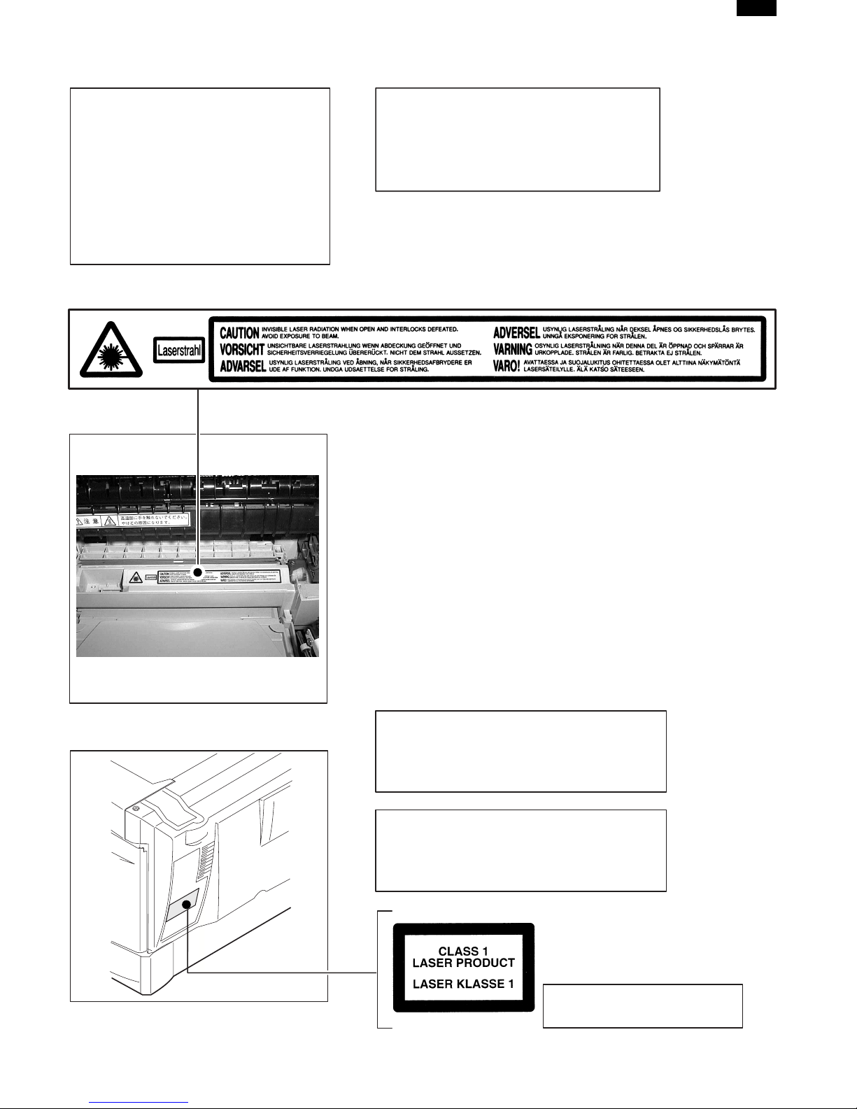
CAUTION
This product is a class 1 laser product that complies with 21CFR 1040.10 and 1040.11 of the CDRH standard and IEC825. This means that this machine does not produce hazardous laser radiation. The use of
controls, adjustments or performance of procedures other than those specified herein may result in hazardous radiation exposure.
This laser radiation is not a danger to the skin, but when an exact focusing of the laser beam is achieved
on the eye’s retina, there is the danger of spot damage to the retina.
The following cautions must be observed to avoid exposure of the laser beam to your eyes at the time
of servicing.
1) When a problem in the laser optical unit has occurred, the whole optical unit must be exchanged as
a unit, not as individual parts.
2) Do not look into the machine with the main switch turned on after removing the developer unit, toner
cartridge, and drum cartridge.
3) Do not look into the laser beam exposure slit of the laser optical unit with the connector connected
when removing and installing the optical system.
4) The middle frame contains the safety interlock switch.
Do not defeat the safety interlock by inserting wedges or other items into the switch slot.
LASER WAVE – LENGTH : 780 ∼ 795
Pulse times : 0.481 ms/6 mm
Out put power : 0.20 ± 0.03 mW
CAUTION
INVISIBLE LASER RADIATION,
WHEN OPEN AND INTERLOCKS DEFEATED.
AVOID EXPOSURE TO BEAM.
VORSICHT
UNSICHTBARE LASERSTRAHLUNG,
WENN ABDECKUNG GEÖFFNET UND
SICHERHEITSVERRIEGELUNG ÜBERBRÜCKT.
NICHT DEM STRAHL AUSSETZEN.
VARO !
AVATTAESSA JA SUOJALUKITUS
OHITETTAESSA OLET ALTTIINA
NÄKYMÄTTÖMÄLLE LASERSÄTEILYLLE ÄLÄ
KATSO SÄTEESEEN.
ADVARSEL
USYNLIG LASERSTRÅLNING VED ÅBNING, NÅR
SIKKERHEDSBRYDERE ER UDE AF
FUNKTION. UNDGÅ UDSAETTELSE FOR
STRÅLNING.
VARNING !
OSYNLIG LASERSTRÅLNING NÄR DENNA DEL
ÄR ÖPPNAD OCH SPÄRREN ÄR URKOPPLAD.
BETRAKTA EJ STRÅLEN. – STRÅLEN ÄR FARLIG.
,
DP1200/1500
At the production line, the output power
of the scanner unit is adjusted to 0.57
MILLI-WATT PLUS 20 PCTS and is
maintained constant by the operation of
the Automatic Power Control (APC).
Even if the APC circuit fails in operation
for some reason, the maximum output
power will only be 15 MILLI-WATT 0.1
MICRO-SEC. Giving an accessible
emission level of 42 MICRO-WATT
which is still-less than the limit of
CLASS-1 laser product.
Caution
This product contains a low power laser
device. To ensure continued safety do not
remove any cover or attempt to gain access
to the inside of the product. Refer all
servicing to qualified personnel.
The foregoing is applicable only to the 220V
230V model and 240V model.
model
VAROITUS! LAITTEEN KÄYTTÄMINEN MUULLA
KUIN TÄSSÄ KÄYTTÖOHJEESSA MAINITULLA
TAVALLA SAATTAA ALTISTAA KÄYTTÄJÄN
TURVALLISUUSLUOKAN 1 YLITTÄVÄLLE
NÄKYMÄTTÖMÄLLE LASERSÄTEILYLLE.
VARNING - OM APPARATEN ANVÄNDS PÅ ANNAT
SÄTT ÄN I DENNA BRUKSANVISNING
SPECIFICERATS, KAN ANVÄNDAREN UTSÄTTAS
FÖR OSYNLIG LASERSTRÅLNING, SOM
ÖVERSKRIDER GRÄNSEN FÖR LASERKLASS 1.
LUOKAN 1 LASERLAITE
KLASS 1 LASER APPARAT

CONTENTS
1. GENERAL ................................................................................................................... 1-1
1. DP1200/1500 major functions .......................................................................................... 1-1
2. System Configuration ....................................................................................................... 1-1
2. SPECIFICATIONS ....................................................................................................... 2-1
1. Basic specifications of copier ........................................................................................... 2-1
3. CONSUMABLE PARTS .............................................................................................. 3-1
1. Supply system table ......................................................................................................... 3-1
2. Environmental .................................................................................................................. 3-1
3. Production control number (lot No.) identification ............................................................. 3-1
4. TD cartridge replacement ................................................................................................. 3-2
4. EXTERNAL VIEWS AND INTERNAL STRUCTURES................................................ 4-1
1. Appearance ...................................................................................................................... 4-1
2. Internal ............................................................................................................................. 4-1
3. Operational panel ............................................................................................................. 4-2
4. Motors and solenoids ....................................................................................................... 4-3
5. Sensors and switches....................................................................................................... 4-4
6. PWB unit .......................................................................................................................... 4-5
7. Cross sectional view......................................................................................................... 4-6
5. UNPACKING AND INSTALLATION
1. A WORD ON COPIER INSTALLATION ............................................................................ 5-1
2. CHECKING PACKED COMPONENTS AND ACCESSORIES .......................................... 5-1
3. UNPACKING .................................................................................................................... 5-1
4. REMOVING PROTECTIVE PACKING MATERIALS ......................................................... 5-1
5. DEVELOPER UNIT INSTALLATION ................................................................................. 5-2
6. TONER CARTRIDGE INSTALLATION.............................................................................. 5-3
7. LOADING COPY PAPER ................................................................................................. 5-3
8. POWER TO COPIER ....................................................................................................... 5-4
9. CONNECTING THE INTERFACE CABLE (DP1200 Only) ............................................... 5-4
6. INSTALLING THE PRINTER DRIVER SOFTWARE (DP1200 Only) ......................... 6-1
1. Description of the printer driver ........................................................................................ 6-1
2. Checking the hardware and software requirements.......................................................... 6-1
3. Installing the printer driver ................................................................................................ 6-1
4. Printer driver group........................................................................................................... 6-3
5. Parallel interface ............................................................................................................... 6-3

7. OPERATIONAL DESCRIPTIONS ............................................................................... 7-1
1. Outline of operation .......................................................................................................... 7-1
2. Scanner section................................................................................................................ 7-2
3. Laser unit ......................................................................................................................... 7-2
4. Fuser section.................................................................................................................... 7-3
5. Paper feed section and paper transport section ............................................................... 7-4
6. Printing process ............................................................................................................... 7-7
8. DISASSEMBLY AND ASSEMBLY .............................................................................. 8-1
1. High voltage section ......................................................................................................... 8-1
2. Operation panel section.................................................................................................... 8-4
3. Optical section .................................................................................................................. 8-5
4. Fusing section .................................................................................................................. 8-6
5. Tray paper feed/Transport section ..................................................................................... 8-9
6. Manual paper feed section ............................................................................................... 8-13
7. Rear frame section ........................................................................................................... 8-17
8. Power section ................................................................................................................... 8-18
9. ADJUSTMENTS .......................................................................................................... 9-1
1. Optical section .................................................................................................................. 9-1
2. Copy density adjustment .................................................................................................. 9-8
3. High voltage adjustment ................................................................................................... 9-9
10. SIMULATION, TROUBLE CODES .............................................................................. 10-1
1. Entering the simulation mode ........................................................................................... 10-1
2. List of simulations ............................................................................................................. 10-2
3. Contents of simulations .................................................................................................... 10-3
4. TROUBLE CODES........................................................................................................... 10-13
11. USER PROGRAM ....................................................................................................... 11-1
12. MAINTENANCE .......................................................................................................... 12-1
1. Maintenance table ............................................................................................................ 12-1
2. Maintenance display system ............................................................................................ 12-1
13. ELECTRICAL SECTION ............................................................................................. 13-1
1. Block diagram................................................................................................................... 13-1
2. Circuit descriptions ........................................................................................................... 13-3
14. CIRCUIT DIAGRAM .................................................................................................... 14-1
DP1200/1500
[1]GENERAL
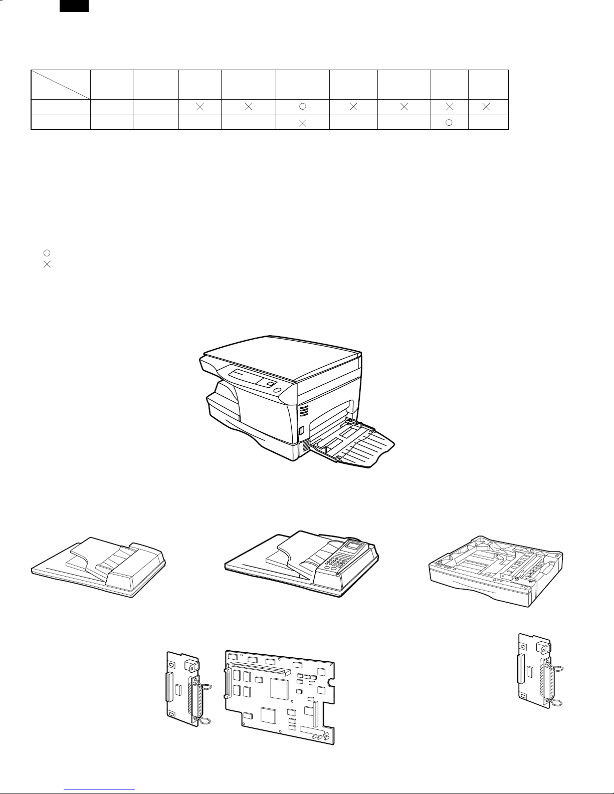
1.DP1200/1500 major functions
Item
Model
DP1200 12CPM MB
DP1500 15CPM MB Opt Opt Opt
Descriptions of items
CPM: Copy speed (Copies Per Minute)
SB/MB: SB = Manual feed single bypass, MB = Manual feed multi bypass
2 tray:Second cassette unit. The 1 tray unit (MY-1019) is optionally available.
SPF (ADF): Original feed unit (Automatic document feeder)
GDI with USB:GDI printer function with USB. The GA-1090 (GDI + USB kit) is optionally available.
SOPM:Scan One Print Many function (Many copies are made by one scan.)
PCL6 with USB:PCL printer function with USB. The GA-1100 (PCL6 + USB kit) is optionally available.
FAX: FAX unit. The GD-1100 (FAX unit) is optionally available.
Descriptions of table
Standard provision
:
No function or no option available
:
Opt: Option
* PCL6 with USB (GA-1100) + FAX (GD-1100) is not available.
CPM SB/MB 2 tray SPF (ADF)
GDI without
USB
GDI with
USB
PCL6 with
USB
Opt
2. System Configuration
SOPM
FAX
Opt
(Options)
MR-2013
(DP-1200/1500)
GD-1100
GA-1100
MY-1019
GA-1090
1 – 1
[2]SPECIFICATIONS
1.Basic specifications of copier
A.Basic specifications
Item Spec.
Type Desktop
Copy system Dry, electrostatic
Segment (class) Digital personal copier
External dimensions (W x D x H) (mm)
Weight
B.Operation specification
SectionItem Details Spec.
Paper feed
system
Paper size A4, B5, A5 (Landscape)
Paper weight 56 – 80g/m
Paper feed capacity 250 sheets
Kinds Standard paper, specified paper, recycled paper
Remark User adjustment of paper guide available
Paper size A4, B5, A5, B6, A6 (Landscape)
Paper weight 52 – 128g/m
Paper feed capacity 50 sheets
Kinds 1
Remark User adjustment of paper guide available
Paper size 8-1/2" x 14", 8-1/2 x 11", 8-1/2" x 5-1/2" (Landscape)
Paper weight 15 – 21 lbs.
Paper feed capacity 250 sheets
Kinds Standard paper, specified paper, recycled paper
Remark User adjustment of paper guide available
Paper size
Paper weight 14 – 34.5 lbs.
Paper feed capacity 50 sheets
Kinds 1
Remark User adjustment of paper guide available
Paper
feed
section
Tray paper feed
section
AB system
Multi bypass paper
feed section
Tray paper feed
section
Inch system
Multi bypass paper
feed section
DP1200: 293mm x 518mm x 445mm (TBD)
DP1500: 293mm x 518mm x 483mm (TBD)
DP1200: Approx. 17.4kg (TBD)
DP1500: Approx. 19kg (TBD)
DP1200, DP1500: 1 tray (250 sheets) + multi bypass (50 sheets)
Standard paper, specified paper, recycled paper, OHP, Label,
8-1/2" x 14", 8-1/2 x 11", 8-1/2" x 5-1/2", 3-1/2" x 5-1/2"
(Landscape)
Standard paper, specified paper, recycled paper, OHP, Label,
DP1200/1500
2
2
Postal card
Postal card
1:OHP, Label, Postal card: each 1 pc.
As special media have wide variety of forms by country or region, they may not be used in some cases.
2 – 1

DP1200/1500
Section Item Details Spec.
Exit way Face down
Paper exit section
Capacity of output
tray
Original set Center Registration (left edge)
Max. original size B4 (10″ × 14″)
Originals
Original kinds Sheet and book
Original size
detection
Scanning system CCD sensor scanning by lighting lamp scanner
CCD sensor Resolution 400 dpi
Optical
section
Scanning
section
Lighting lamp
Type Xenon lamp
Voltage 1.5kV
Power consumption 11 ± 3W
Gradation 256 gradations/8bit
Writing
section
Writing system Writing to OPC drum by the semiconductor laser
Laser unit Resolution 600 dpi
Photoconductor
Type OPC (30φ)
Life25k
Image forming
Charger
Charging system Saw -tooth charging with a grid, / (–) scorotron discharge
Transfer system (+) DC corotron system
Separation system (–) DC corotron system
Developing Developing system Dry, 2-component magnetic brush development system
Cleaning Cleaning system Counter blade system (Counter to rotation)
Fusing system Heat roller system
Upper heat roller Type Teflon roller
Fusing section
Lower heat roller Type Silicon rubber roller
Type Halogen lamp
Heater lamp
Voltage100V/240V
Power consumption 800W
Power source
Voltage Local AC voltage
Frequency Common use for 50 and 60Hz
Max.DP1200/DP1500: 1000W
Electrical section
Power consumption
Average (operating) *
Stand-by mode
(initial condition) *
Pre-heat mode *
1)
Auto power shut-off mode *
*1) May fluctuate due to environmental conditions and the input voltage.
1)
1)
1)
DP1500: 310Wh/H, DP1200: 270Wh/H
100 sheets
None
DP1200/DP1500: 70Wh/H
DP1200/DP1500: 40Wh/H
DP1200/DP1500: 18Wh/H
2 – 2
C.Copy performance
Section Item Details Spec.
Copy magnification
Manual steps (manual,
photo)
Copy speedFirst copy time
AB system: A4
(Landscape)
B5 (Landscape)Copy speed (CPM)
Inch system 8-1/2”
× 14” (Landscape)
8-1/2” × 11”
(Landscape)
Max. continuous copy
quantity
Fixed magnification ratios
Zooming magnification ratios 50 ~ 200% (151 steps in 1% increments)
Copy speed (CPM)
Copy speed (CPM)
Copy speed (CPM)
Void area
DP1200/1500
3R + 2E (AB system: 50, 70, 81, 100, 141, 200%)
(Inch system: 50, 64, 78, 100, 129, 200%)
5 steps
9.6 sec. or below (A4), 9.4 sec. or below (8-1/2"
Tray paper feed
Manual paper feed
Same size DP1200: 12DP1500: 15
EnlargementDP1200: 12DP1500: 15
Reduction DP1200: 11DP1500: 15
Same size DP1200: 12DP1500: 15
EnlargementDP1200: 12DP1500: 15
Reduction DP1200: 12DP1500: 15
Same size DP1200: 10DP1500: 12
EnlargementDP1200: 10DP1500: 12
Reduction DP1200: 10DP1500: 12
Same size DP1200: 12DP1500: 15
EnlargementDP1200: 12DP1500: 15
Reduction DP1200: 12DP1500: 15
Leading edge 1 4 mm
Trailing edge
14") (Pre-heat mode: 16 sec. or below / Auto power-
shut-off mode: 23 sec. or below)
10.0 sec (Pre-heat mode: 16 sec. or below / Auto
power-shut-off mode: 23 sec. or below)
99
4 mm or less
Void
Image loss
Side edge void area
OC mode Leading edge
SPF mode
Leading edge
4 mm or less
(per side)
Same size: 3.0mm or less / Enlarge (200%): 2.0mm
or less / Reduction (50%): 6.0mm or less
Same size: 4.0mm or less / Enlarge (200%): 3.0mm
or less / Reduction (50%): 8.0mm or less
2 – 3
DP1200/1500
[3]CONSUMABLE PARTS
1.Supply system table
No. Name Model name Life Package unit Remark
1 Toner Cartridge PS-ZT1200
2 Developer D-1200 10
3 Drum Kit OD-1200 10
6.5K
25K
(6%)
25K
10 Life based on 6% coverage of A4 original.
2.Environmental
The environmental conditions for assuring the copy quality and the
machine operations are as follows:
(1) Normal operating condition
Temperature: 20°C~25
Humidity: 65 5%RH
(2) Acceptable operating condition
Humidity (RH)
85%
60%
20%
10°C 30°C 35°C
(3) Transportation condition
Humidity (RH)
90%
60%
3.Production control number (lot No.)
identification
áDeveloping cartridgeñ
Production month
Production day
Destination code
(Dealer, distributor, OEM, etc.)
Production place
(SOCC: Fixed to B.)
End digit of year
Version No.
*:Destination
Division No.
EX Destination
Option Destination
áDrum cartridgeñ
The label on the drum cartridge shows the date of production.
(SOCC production)
A same pack G
B same pack H
AP
BQ
15%
–25°C 30°C 40°C
(4) Supply storage condition
Humidity (RH)
90%
20%
–5°C 45°C
Production month
Production day
Destination code
(Dealer, distributor, OEM, etc.)
Production place
(SOCC: Fixed to B.)
End digit of year
Version No.
áJAPAN productionñ
Ver. A 9 1 1 0001 X
Production month
(1-9=Jan. -Sep. 0=Oct. X=Nov. Y=Dec)
Serial number of month
Fixed to 1.
Pack division
(See table below)
End digit of year
Version No.
3 – 1
DP1200/1500
Division No.
Ex production 1
Option 2
Same pack 3
Production control
label attachment position
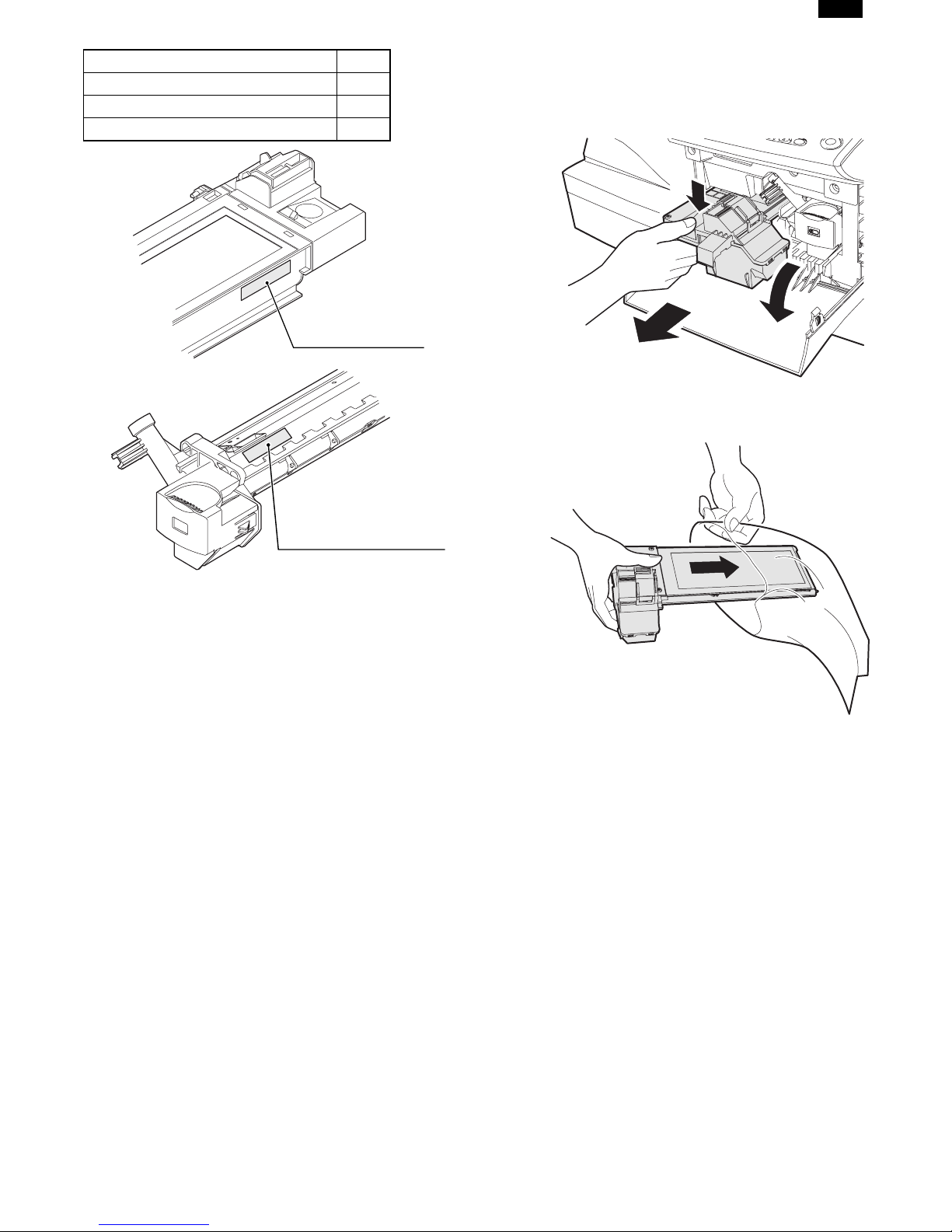
4. TD cartridge replacement
1) Open the front and side cabinets of the copier.
2) Keep holding Toner lover, and
3) Carefully pull out Toner unit from the copier.
2
3
1
4) Put Toner unit in a collection bag immediately after removing it from
the copier
Production control
label attachment position(*1)
∗1 The production control label is not attached to the cartridge of a
China product.
Note: Never carry exposed Toner unit. Be sure to put it in the col-
lection bag.
3 – 2
DP1200/1500
[4] EXTERNAL VIEWS AND INTERNAL STRUCTURES
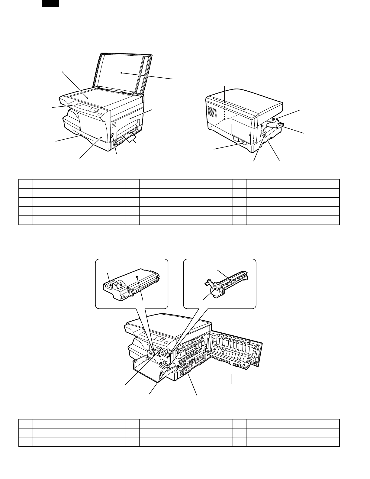
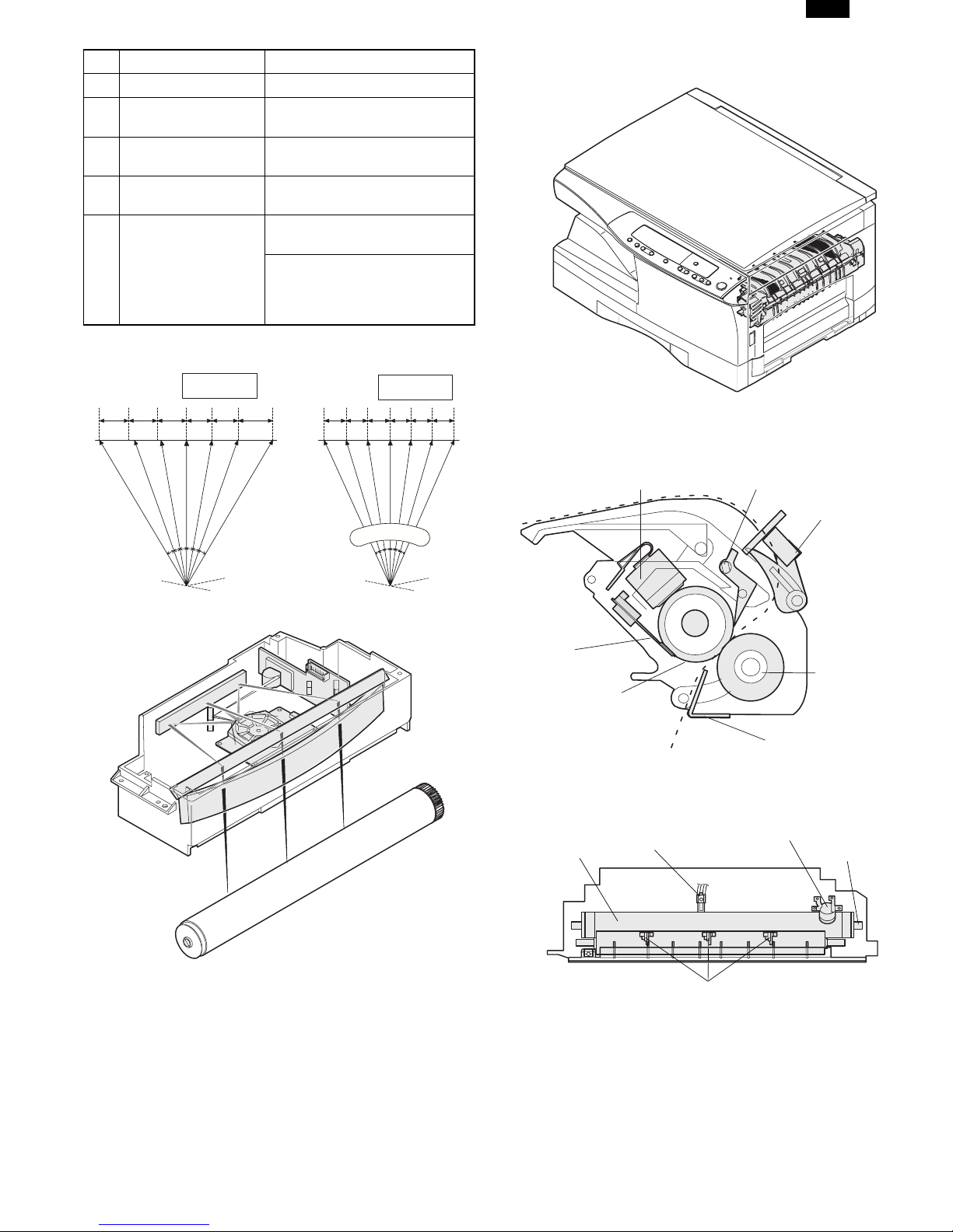
1. Appearance
(1)
(2)
(4)
(6)
(5)
(1) Original table (2) Original cover (3) Side cover
(4) Operation panel (5) Front cover (6) Paper tray
(7) Side cover open button (8) Paper guides (9) Handle
(10) Paper output tray (11) Paper output tray extension (12) Power cord socket
(13) Power switch
(7)
(3)
(8)
(12)
(9)
(13)
(9)
2. Internal
(10)
(11)
(1)
(2)
(5)
(6)
(1) TC cartridge lock release button (2) TD cartridge (3) Drum cartridge
(4) Drum cartridge handle (5) Paper feed roller (6) Fusing unit release lever
(7) Charger cleaner (8) Transfer charger
(3)
(4)
(8)
(7)
4 – 1
3. Operational panel
DP1200/1500
(1) (2) (3)
(14)
(4)
(15)
(5)
(6)
(7) (8)
(16) (17) (18) (19)
(6)
(9)
(10)
(11)
(12)
(13)
Inch system
Exposure mode selector key
(1)
and indicators
(4) SPF indicator (5) SPF misfeed indicator (6)
(7) Zoom indicator (8) Copy ratio display (%) key (9) Display
(10) ON LINE indicator (11) ON LINE key (12) DATA indicator
(13) Power save indicator (14) Tray select key (15) Paper feed location indicators
(16) Zoom keys (17) Copy quantity keys (18) Clear key
(19) Print key and ready indicator
Light and dark keys and
(2)
exposure indicators
(3) Alarm indicators
Copy ratio selector key and
copy ratio indicators
∗1
∗1
Developer replacement required indicator
Misfeed indicator
Toner cartridge replacement required indicator
Maintenance indicator
∗2 ON: Indicates that the machine is in the energy saving (pre-heat) mode.
Blink: Indicates that the machine is in the process of resetting from the energy saving mode or just after supplying the power.
OFF: Indicates that resetting from the energy saving mode is completed and that the fusing temperature is in ready state.
The combinations of the above display lamps are as follows: (● = ON, ✕ = OFF)
Lamp Immediately after power ON Ready Copying
Pre-heat lamp Blink ✕✕
Ready lamp ●●✕
Other lamps ●●●
Copy is started during
resetting from energy
saving mode
Lamp
Energy saving mode (Pre-
heating)
Energy saving mode
(Auto power shut off)
Resetting from energy
saving mode
Pre-heat lamp ●●Blink Blink
Ready lamp ●✕●✕
Other lamps ●✕●●
4 – 2
DP1200/1500
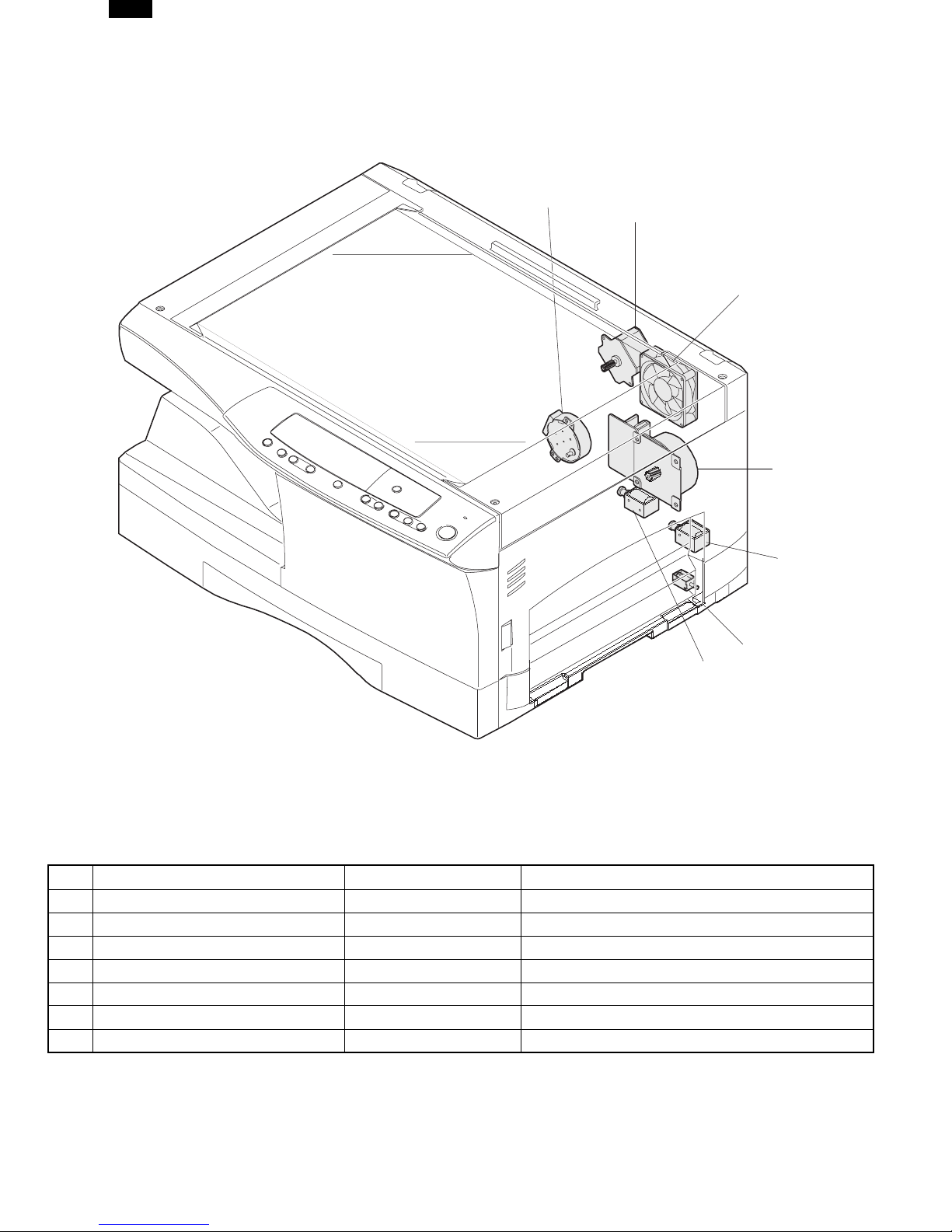
4. Motors and solenoids
(3)
(2)
(4)
(1)
(5)
(7)
(6)
No. Part name Control signal Function,operation
(1) Main motor MM Drives the copier.
(2) Mirror motor MRMT Drives the optical mirror base (scanner unit).
(3) Toner motor TM Supplies toner.
(4) Cooling fan motor VFM Cools the optical section.
(5) Resist roller solenoid RRS Resist roller rotation control solenoid
(6) Paper feed solenoid CPFS1 Cassette Paper feed solenoid
(7) Multi paper feed solenoid MPFS Multi manual pages feed solenoid
4 – 3
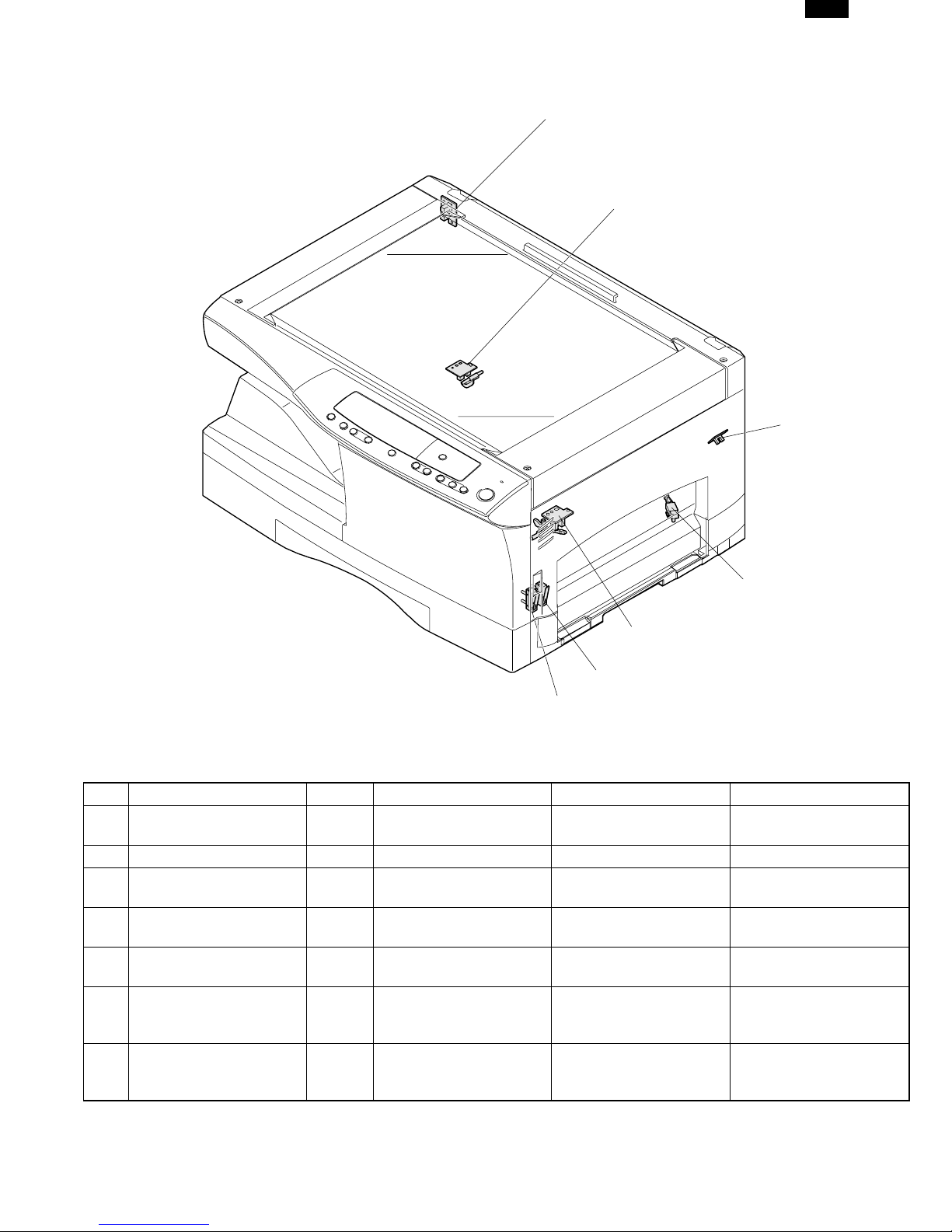
5. Sensors and switches
DP1200/1500
(1)
(2)
(3)
(4)
(5)
(6)
(7)
No. Name Signal Type Function Output
Mirror home position
(1)
sensor
(2) POD sensor POD Transmissions sensor Paper exitdetection “H” at paper pass
(3) PPD2 sensor PPD2 Transmission sensor
Cassette detection
(4)
switch
(5) PPD1 sensor PPD1 Transmission sensor
(6) Door switch DSW Micro switch
(7) Door switch DSW Micro switch
MHPS Transmission sensor
CED1 Microswitch
Mirror (scanner unit)
home position detection
Paper transport
detection 2
Cassette installation
detection
Paper transport
detection 1
Door open/close
detection (safety switch
for 5V)
Door open/close
detection (safety switch
for 24V)
“H” at home position
“L” at paper pass
“H” at cassette insertion
“L” at paper pass
1 or 0V of 5V at door
open
1 or 0V of 24V at door
open
4 – 4
DP1200/1500
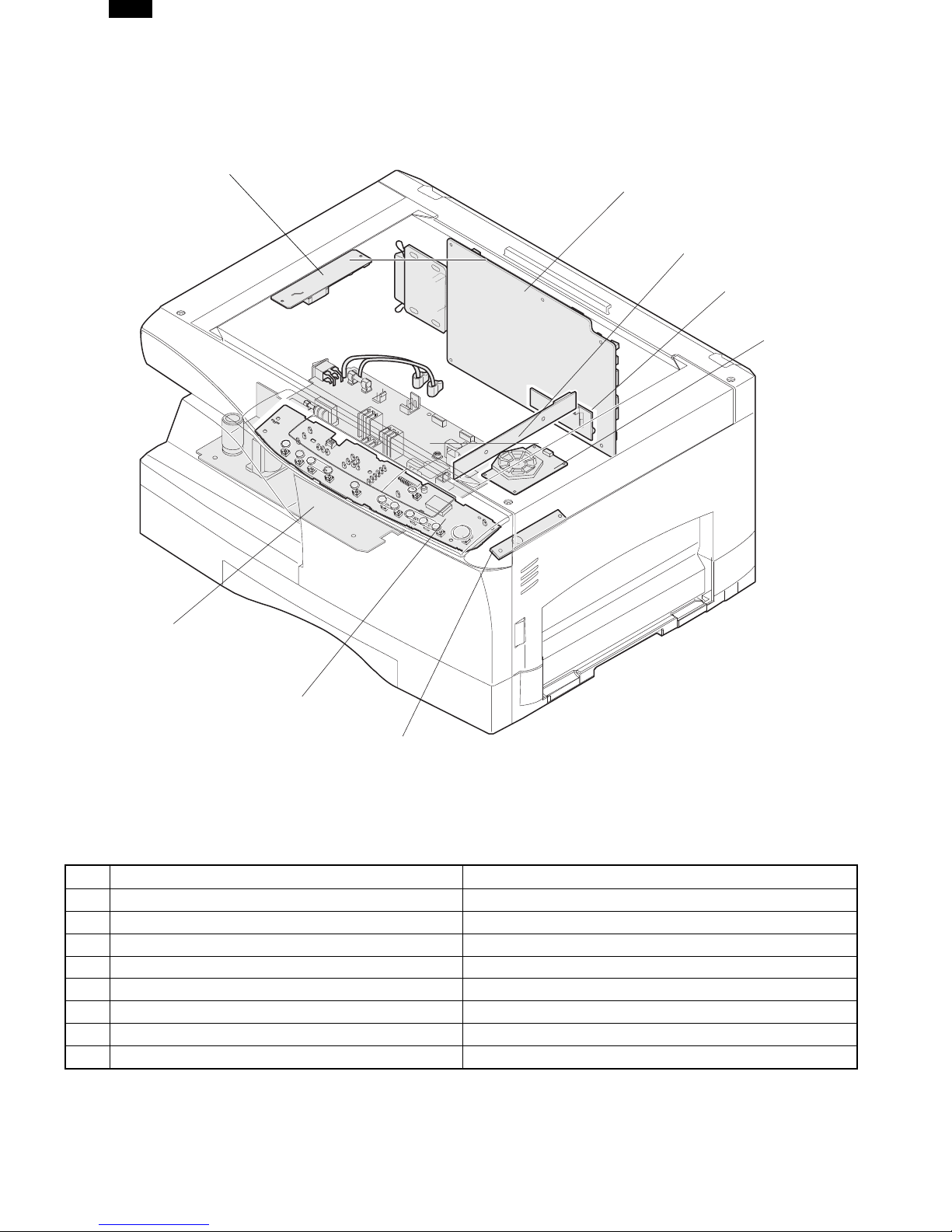
6. PWB unit
(1)
(2)
(5)
(8)
(6)
(4)
(3)
(7)
No. Name Function
(1) Exposure lamp invertor PWB Exposure lamp (Xenon lamp) control
(2) Main PWB (MCU) Copier control
(3) Operation PWB Operation input/display
(4) Power PWB AC power input, DC voltage control, High voltage control
(5) CCD sensor PWB For image scanning
(6) LSU motor PWB For polygon motor drive
(7) TCS PWB For toner sensor control
(8) LSU PWB For laser control
4 – 5
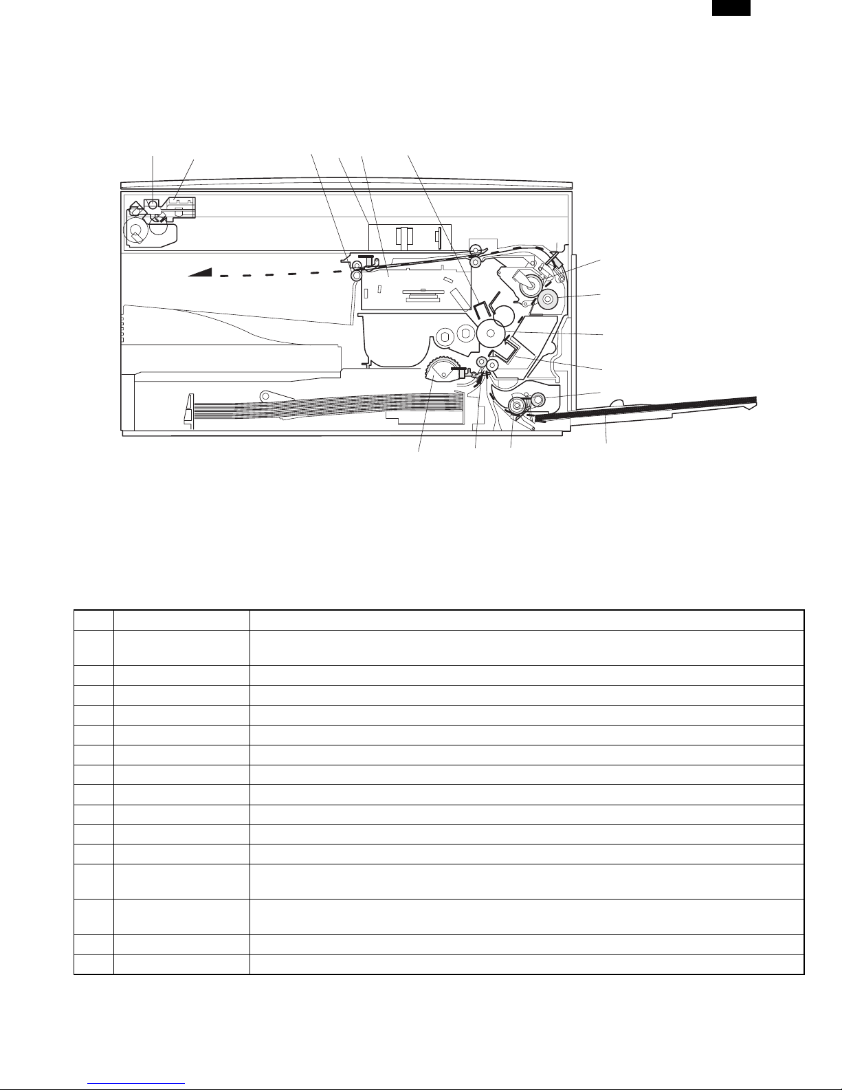
7. Cross sectional view
DP1200/1500
(2)
(1)
(5)
(3)
(4)
(6)
(15)
(14)
(13)
(7)
(8)
(9)
(10)
(11)
(12)
No. Part name Function and operation
(1) Scanner unit
(2) Exposure lamp Exposure lamp (Xenon lamp) Illuminates original
(3) Lens unit Scans the original image with the lens and the CCD.
(4) LSU (Laser unit) Converts the original image signal into laser beams and writes onto the drum.
(5) Paper exit roller Roller for paper exit
(6) Main charger Provides negative charges evenly to the drum surface.
(7) Heat roller Fuses toner on the paper. (Teflon roller)
(8) Pressure roller Fuses toner on the paper. (Silicon rubber roller)
(9) Drum Forms images.
(10) Transfer unit Transfers images onto the drum.
(11) Pickup roller Picks up the manual feed paper. (In multi feed only)
(12)
(13)
(14) PS roller unit Takes synchronization between the lead edge and the rear edge of the paper.
(15) Paper feed roller Picks up a sheet of paper from the cassette.
Manual paper feed
tray
Manual paper feed
roller
Illuminates the original with the copy lamp and passes the reflected light to the lens unit
(CCD).
Tray for manual feed paper
Transport the paper from the manual paper feed port.
4 – 6
DP1200/1500
[5] UNPACKING AND INSTALLATION
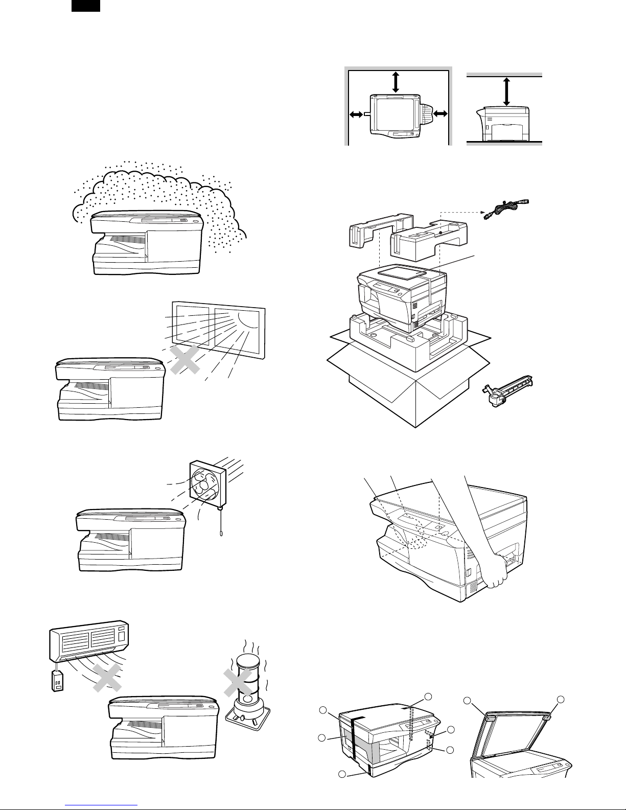
1. A WORD ON COPIER INSTALLATION
Improper installation may damage the copier. Please note the
following during initial installation and whenever the copier is
moved.
Do not install your copier in areas that are:
● damp, humid, or very dusty
● exposed to direct sunlight
Be sure to allow the required space around the machine for
servicing and proper ventilation.
8"(20cm)
8"(20cm)
4"
(10cm)
4"
(10cm)
2. CHECKING PACKED COMPONENTS AND
ACCESSORIES
Open the carton and check if the following components and accessories are included.
Power cord
Operation manual
(CD-ROM : DP1200 Only)
Copier
● poorly ventilated
● subject to extreme temperature or humidity changes, e.g.,
near an air conditioner or heater.
Drum cartridge
(installed in copier)
3. UNPACKING
Unpack the copier and carry it to the installation location by
holding the handles on both sides of the copier.
4. REMOVING PROTECTIVE PACKING
MATERIALS
1) Remove pieces of tape (a), (b), (c), (d) and (e) and protec-
tive cover (f). Then open the original cover and remove
protective materials (g) and (h).
c
a
g
h
f
e
d
b
5 – 1
DP1200/1500
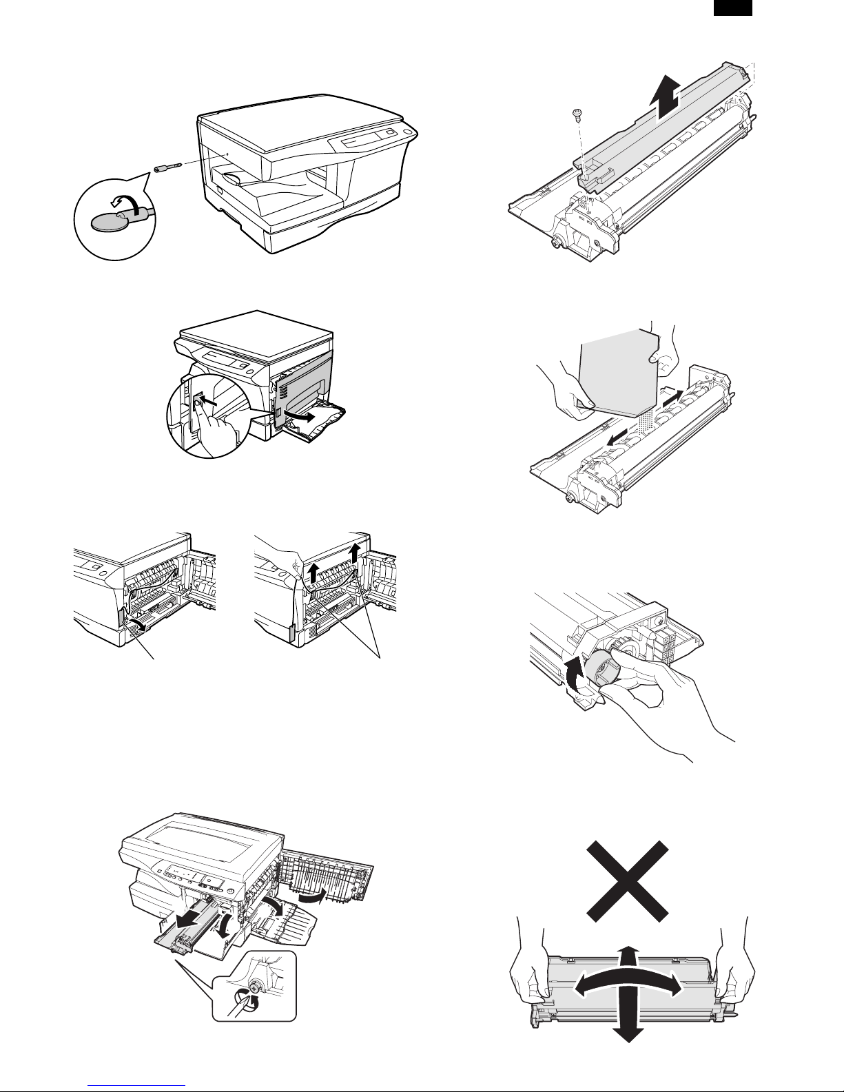
2) Use a coin (or suitable object) to remove the screw.
Store the screw in the paper tray because it will be used if
the copier has to be moved.
3) Open the bypass tray and then open the side cover whilst
pressing the side cover open button.
8) Remove Upper developer unit.
9) Shake the aluminum bag to stir developer
10) Supply developer from the aluminum bag to the top of the
MX roller evenly.
4) Remove the CAUTION tape from the front cover and
remove the two protective pins from the fusing unit by pulling the strings upward one at a time.
CAUTION tape
Protective pins
5. DEVELOPER UNIT INSTALLATION
1) 2) 3) Open the side and front cabinets of the copier.
4) Remove the locking tape of the developer unit.
5) Remove the screw which is fixing the copier and
Developer unit.
6) Remove Developer unit slowly from the copier.
Note: Be careful not to splash developer outside Developer
unit.
11) Attach Upper developer unit and fix it with a screw.
12) Rotate the MG roller gear to distribute developer evenly.
Note: Never rotate the gear in the reverse direction.
Note: When carrying Developer unit, do not tilt it extremely
as shown with the arrow in the figure below.
(Prevention of splash of developer)
5
1
3
4
7) Remove the screw (1 pc).
2
5 – 2
DP1200/1500
13) Insert Developer unit carefully into the copier.
Note: Quick insertion may result in splash of developer. Be
sure to insert carefully.
14) Confirm that Developer unit is completely inserted to the
bottom of the machine, fix Developer unit and the machine
with a screw.
15) Completion of Developer unit installation
6. TONER CARTRIDGE INSTALLATION
1) To prevent against uneven distribution of toner, hold Toner
unit with both hands and shake it several times horizontally.
2) Hold the section of Toner unit shown in the figure below,
remove the packing tape, and remove the cushion.
3) Remove the tape securing the shutter, and pull out the
cushion in the arrow direction.
Note: Do not hold and carry the shutter. Otherwise the shut-
ter may drop and Toner unit may drop.
7) Completion of Toner unit installation
Close the front and side cabinets.
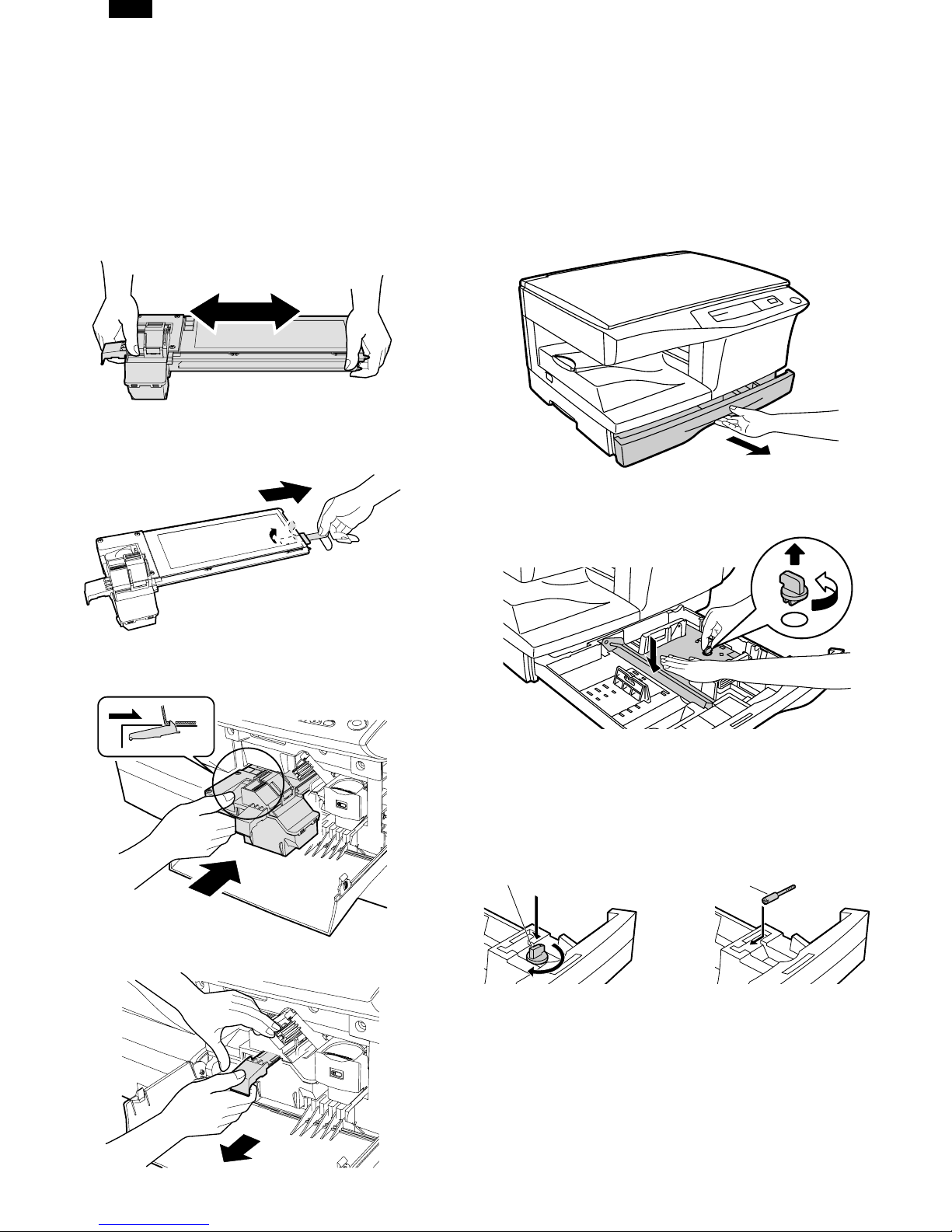
7. LOADING COPY PAPER
Note: This copier is equipped with two paper trays. Load copy
paper into the two paper trays.
1) Raise the handle of the paper tray and pull the paper tray
out until it stops.
2) Remove the pressure plate lock. Rotate the pressure plate
lock in the direction of the arrow to remove it while pressing
down the pressure plate of the paper tray.
4) Insert Toner unit carefully into the copier.
5) Insert until the hook is engaged with the copier as shown in
the figure below.
6) Pull out the shutter in the arrow direction.
3) Store the pressure plate lock which has been removed in
step 2 and the screw which has been removed when unpacking (see page 5-2, step 2 of REMOVING PROTECTIVE PACKING MATERIALS) in the front of the paper tray.
To store the pressure plate lock, rotate the lock to fix it on
the relevant location.
Pressure plate lock
Screw
4) Adjust the paper guides on the paper tray to the copy paper
width and length.
Squeeze the lever of paper guide (A) and slide the guide to
match with the width of the paper.
Move paper guide (B) to the appropriate slot as marked on
the tray.
5 – 3
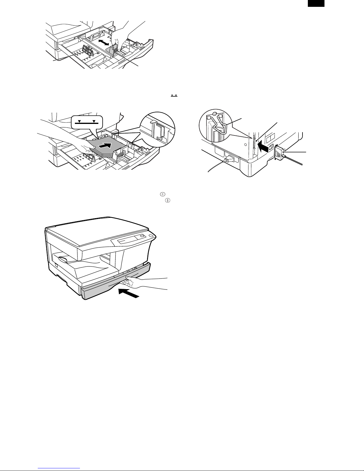
Paper guide (B)
Paper guide (A)
5) Fan the copy paper and insert it into the tray. Make sure the
edges go under the corner hooks.
Note: Do not load paper above the maximum height line ( ).
Exceeding the line will cause a paper misfeed.
DP1200/1500
9. CONNECTING THE INTERFACE CABLE
(DP1200 Only)
● For specifications of the parallel interface, see page 6-3.
1) Check that the power switches of both the printer and the
computer are in the OFF position.
2) Plug the parallel interface cable into the printer interface
connector. Fasten the two bail clips at the side of the printer
connector to hold the interface connector in place.
3) Plug the other end of the cable into the parallel interface
connector on your computer. (Refer to your computer
manual for details.)
6) Gently push the paper tray back into the copier.
Note: After loading copy paper, to cancel the blinking “P”
without restarting copying, press the clear ( ) key.
The “P ” in the disp lay wil l go out and t he rea dy ( ) indicator will light up.
Bail clip
Parallel interface connector
Interface connector
Cable
● The printer sends and receives data bi-directionally and
at high speed. Some switch boxes and pass-through
devices cannot support high-speed, bi-directional transfer of data, and using them may cause printing errors.
8. POWER TO COPIER
1) Ensure that the power switch of the copier is in the OFF
position. Insert the attached power cord into the power cord
socket at the rear of the copier.
2) Plug the other end of the power cord into the nearest outlet.
5 – 4
DP1200/1500
[6] INSTALLING THE PRINTER DRIVER
SOFTWARE (DP1200 Only)
1. Description of the printer driver
The printer driver is the software program which runs the
printer. It converts the data in your file into information that the
printer can understand. It also controls communication between
the printer and computer as the data is printed.
2. Checking the hardware and software requirements
You will need the following hardware and software in order to
install the printer driver.
Computer type IBM PC/AT or compatible
computer equipped with a
bi-directional parallel
interface and CD-ROM
drive
Windows type Windows 3.1x, Windows
95, Windows 98, Windows
NT 4.0
CPU 486DX 66 MHz or better
Physical RAM Windows 95, Windows
3.1x: 8 MB (16 MB or
more is recommended.)
Windows 98, Windows NT
4.0: 16MB (32MB or more
is recommended.)
Virtual storage (swap file) 8 MB or moreDisplay 640
´ 480 dots (VGA) or better
Hard disk free space 10 MB or more
The printer driver included in this product cannot be used
under Windows NT3.5x, OS/2, pure MS-DOS and other
operating systems which are not described above.
If you are using some of your computers memory as a RAM
drive, the printer driver may not be allocated the correct
amount of memory. In such a case, reduce the size of your
RAM disk, or do not use the RAM disk. Please refer to your
MS Windows documentation for further information.
3. Installing the printer driver
The software for your printer is provided on CD-ROM.
Before installing the printer driver, be sure to check the following items.
Is the printer connected properly to the computer?
Does the printer have paper?
Is there another GDI printer driver or Windows Printing
System printer driver already installed? If installed,
change the printer port setting.
In this description, the following drive configuration is supposed. Specify proper drives depending on the configuration of
your computer.
Drive R: CD-ROM drive (installation source)
Drive C: Hard disk drive (installation destination)
A. Windows 95/Windows NT 4.0:
1) Load paper into the paper tray of the printer.
2) Turn on the printer.
3) Turn on your computer and start Windows.
Before installing the printer driver, be sure to close all
other applications which may be open.
4) When using Windows 95 on a personal computer with
plug & play
will appear. Insert the installation CD-ROM into the CDROM drive. Click the Next button and follow the on-screen
instructions. Proceed to step 7. If the "Copying Files" window appears during this operation, enter R:\ (if the CDROM is designated as drive R) and click the OK button.
If you use Windows 95 and the "New Hardware Found"
window will appear, click the Driver from Disk Provided
by Hardware Manufacturer button and then click OK.
Proceed to step 6.
If you use Windows 95 and the screen shown above or
the "New Hardware Found" window does not appear,
proceed to step 5.
If you use Windows NT 4.0, proceed to step 5.
Plug & play
This feature is effective if both the computer and
peripheral equipment are equipped with IEEE 1284 compliant parallel interface.
The screen displayed depends on the version of Windows.
5) Insert the installation CD-ROM into the CD-ROM drive.
Click the Start button and select Run. When the screen
shown below appears, type R:\SETUP (if the CD-ROM is
designated as drive R) and click the OK button. Proceed
to step 7.
*
, the "Update Device Driver Wizard" window
6 – 1
DP1200/1500
6) "Installation from CD-ROM" window will appear. Insert the
installation CD-ROM into the CD-ROM drive. Type R:\ (if
the CD-ROM is designated as drive R) and click the OK
button. Proceed to step 7.
7) The installation program will start. To install the printer
driver to the default folder, click the Next button. To select
a different folder, select Browse and type in the new path
and folder name. Click OK and say YES to create the
folder, select the Next button to continue.
8) On the display, you will see "printer port to be used". Normally, this is LPT1 and it is selected automatically.
Ensure that Yes is checked to use the printer as the
default printer.
Finally click the Next button.
9) A "Confirm installation" window will be displayed. To continue installation, click the Yes button.
5) Select Search for the best driver for your device and
click the Next button.
6) Insert the installation CD-ROM into the CD-ROM drive.
Select the CD-ROM drive and click the Next button.
7)Windows driver file search will find the device TOSHIBA
e-STUDIO Series. Click the Next button. Proceed to step 9.
8) Insert the installation CD-ROM into the CD-ROM drive.
Click the Start button and select Run. When the window
shown below appears, type R:\SETUP (if the CD-ROM is
designated as drive R) and click the OK button. Proceed
to step 9.
10) When the installation is complete, you will be asked
whether or not to print a test page. If you wish to do so,
click the Yes button. At this time, ensure that paper is
loaded in the paper tray.
11) If the test print completes successfully, click the Finish
button. "The installation of the
TOSHIBA e-STUDIO
Series
Software is complete." window will be displayed. Click the
OK button.
B. Windows 98:
1) Load paper into the paper tray of the printer.
2) Turn on the printer.
3) Turn on your computer and start Windows.
Before installing the printer driver, be sure to close all
other applications which may be open.
4) When using Windows 98 on a personal computer with
*
plug & play
, the "Add New Hardware Wizard" window will
appear. Click the Next button and follow the on-screen
instructions.
If the "Add New Hardware Wizard" window does not appear, proceed to step 8.
Plug & play: For plug & play information, see page 4-1.
9) The installation program will start. To select a different
folder, select Browse and type in the path and folder
name where the printer driver will be installed. Click OK
and say YES to create the folder, select the Next button
to continue. To install the printer driver to the default
folder, click the Next button.
10) On the display, you will see "printer port to be used". Normally, this is LPT1 and it is selected automatically. Ensure
that Yes is checked to use the printer as the default
printer. Finally click the Next button.
11) A "Confirm installation" window will be displayed. To continue installation, click the Yes button.
12) When the installation is complete, you will be asked
whether or not to print a test page. If you wish to do so,
click the Yes button. At this time, ensure that paper is
loaded in the paper tray.
13) If the test print completes successfully, click the Finish
button. "The installation of the TOSHIBA e-STUDIO Series
Software is complete." window will be displayed. Click the
OK button.
C. Windows 3.1x:
1) Load paper into the paper tray of the printer.
2) Turn on the printer and then start Windows on your computer.
Before installing the printer driver, be sure to close all
other applications which may be open.
6 – 2
DP1200/1500
3)Insert the installation CD-ROM into a CD-ROM drive.
4)Choose File from the Menu bar in Program Manager, and
then choose the Run... command.
5)Type R:\SETUP (if the CD-ROM is designated as drive R)
in the command line box and then click the OK button.
6)Select a directory to which the printer driver will be installed and click the Next button. To install it to the default
directory, click the Next button.
7)A “printer port to be used” window will be displayed. Normally, LPT1 is automatically set.
Then ensure that Yes is checked to use this printer as the
default printer.
8)A “Confirm installation” window will be displayed. To continue installation, click Yes.
9)When the installation is complete, restart Windows.
4.Printer driver group
When the printer driver is installed, the TOSHIBA e-STUDIO Series
printer driver group will be created. This group allows the following functions to be executed.
Uninstall
The printer driver can be uninstalled. If the driver is
uninstalled, printing cannot be performed on the printer.
For proper uninstallation, be sure to use uninstallation program of the printer driver group.
Readme
The latest information on the printer driver is included in
this note. Read the Readme first.
Advanced Settings
See help for application support and application problems
that may occur when printing. See help for the applicable
method of usage.
Status Monitor
The printer state and information on current printing are
displayed on the status monitor window.
DOS Emulation Setup
Status Monitor HELP
DOS Emulation HELP
Advanced Settings HELP
5.Parallel interface
This printer uses a bi-directional parallel interface. Use the supplied interface cable.
Connector
36-pin DDK 57LE-40360-730B (D29) female connector or
equivalent connector
Cable
Shielded type bi-directional parallel interface
For best results,, use a printer interface cable which is
IEEE1284 compliant.
Pin configuration
The pin numbers and signal names are listed in the following table.
18
36 19
Pin No.Signal namePin No.Signal name
1 STB19GND (STB RET)
2DATA120GND (DATA1 RET)
3DATA221GND (DATA2 RET)
4DATA322GND (DATA3 RET)
5DATA423GND (DATA4 RET)
6DATA524GND (DATA5 RET)
7DATA625GND (DATA6 RET)
8DATA726GND (DATA7 RET)
9DATA827GND (DATA8 RET)
ACKNLG28
10
11BUSY29GND (BUSY RET)
12PE (Paper End)30GND (PE RET)
13SLTC31INPRM
AUTO LF32 FAULT
14
15(NC)33(NC)
16GND (0 V)34(NC)
17FG35+5 V
18+5 V36
1
GND
ACKNLG RET)
(
SLTC IN
●Be sure to read “Readme” found in the printer driver group
before starting to print from application programs.
6 – 3
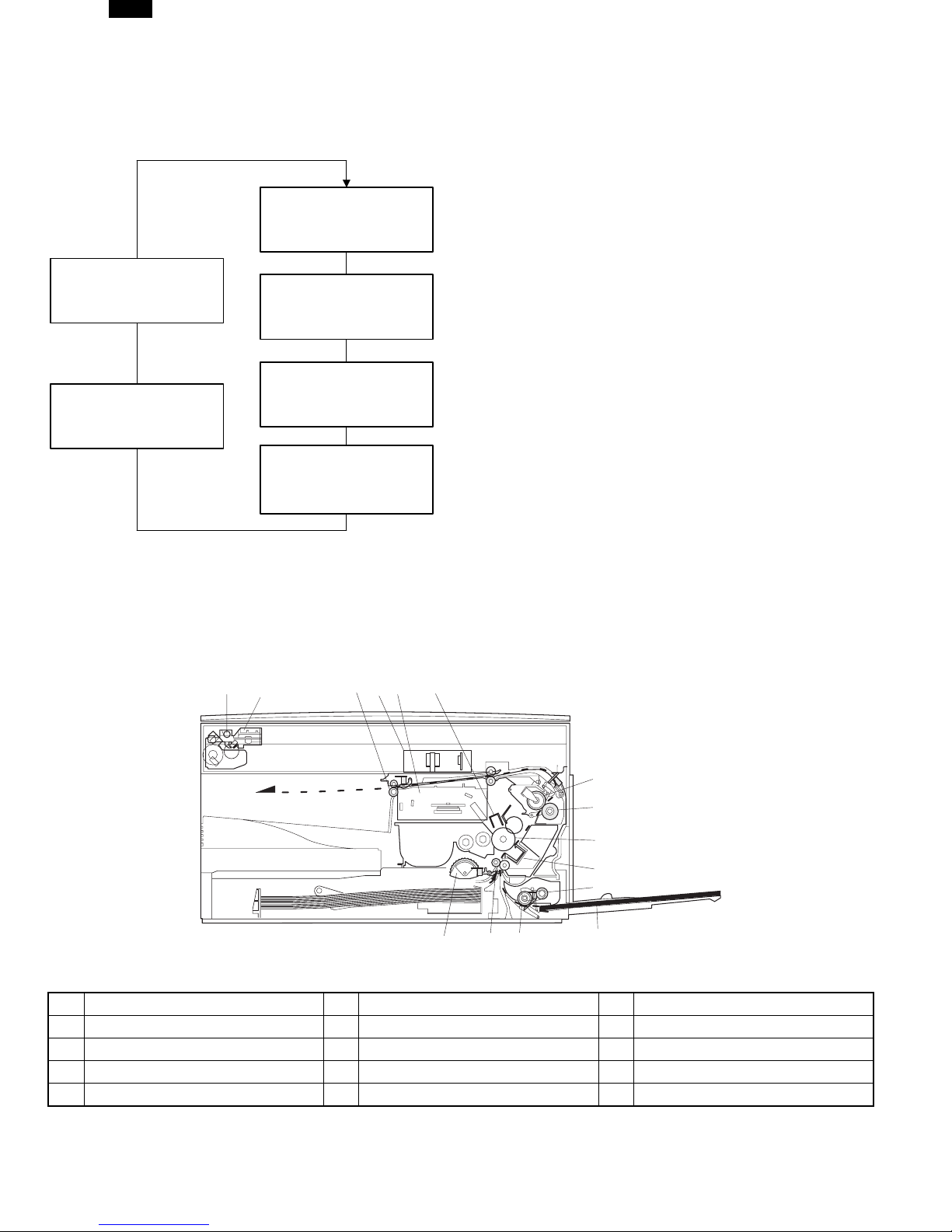
[7]OPERATIONAL DESCRIPTIONS
1.Outline of operation
The outline of operation is described referring to the basic configuration.
(Basic configuration)
DP1200/1500
Operation
section
Printer section
Scanner section
MCU (Main control/image process section)
LSU (Laser unit)
Laser diode, Polygon mirror lens
Laser beam
Process section
Cassette paper
feed section
CCD
Paper exit
Fusing section
Paper transport section
Manual paper
feed section
(Outline of copy operation)
Setting conditions
1)Set copy conditions such as the copy quantity and the copy density with the operation section, and press the COPY button. The information
on copy conditions is sent to the MCU.
Image scanning
2)When the COPY button is pressed, the scanner section starts scanning of images.
The light from the copy lamp is reflected by the document and passed through the lens to the CCD.
Photo signal/Electric signal conversion
3)The image is converted into electrical signals by the CCD circuit and passed to the MCU.
Image process
4)The document image signal sent from the CCD circuit is processed under the revised conditions and sent to the LSU (laser unit) as print data.
Electric signal/Photo signal (laser beam) conversion
5)The LSU emits laser beams according to the print data.
(Electrical signals are converted into photo signals.)
6)The laser beams are radiated through the polygon mirror and various lenses to the OPC drum.
Printing
7)Electrostatic latent images are formed on the OPC drum according to the laser beams, and the latent images are developed to be visible images (toner images).
8)Meanwhile the paper is fed to the image transfer section in synchronization with the image lead edge.
9)After the transfer of toner images onto the paper, the toner images are fused to the paper by the fusing section. The copied paper is discharged
onto the exit tray.
7 – 1
DP1200/1500
2.Scanner section
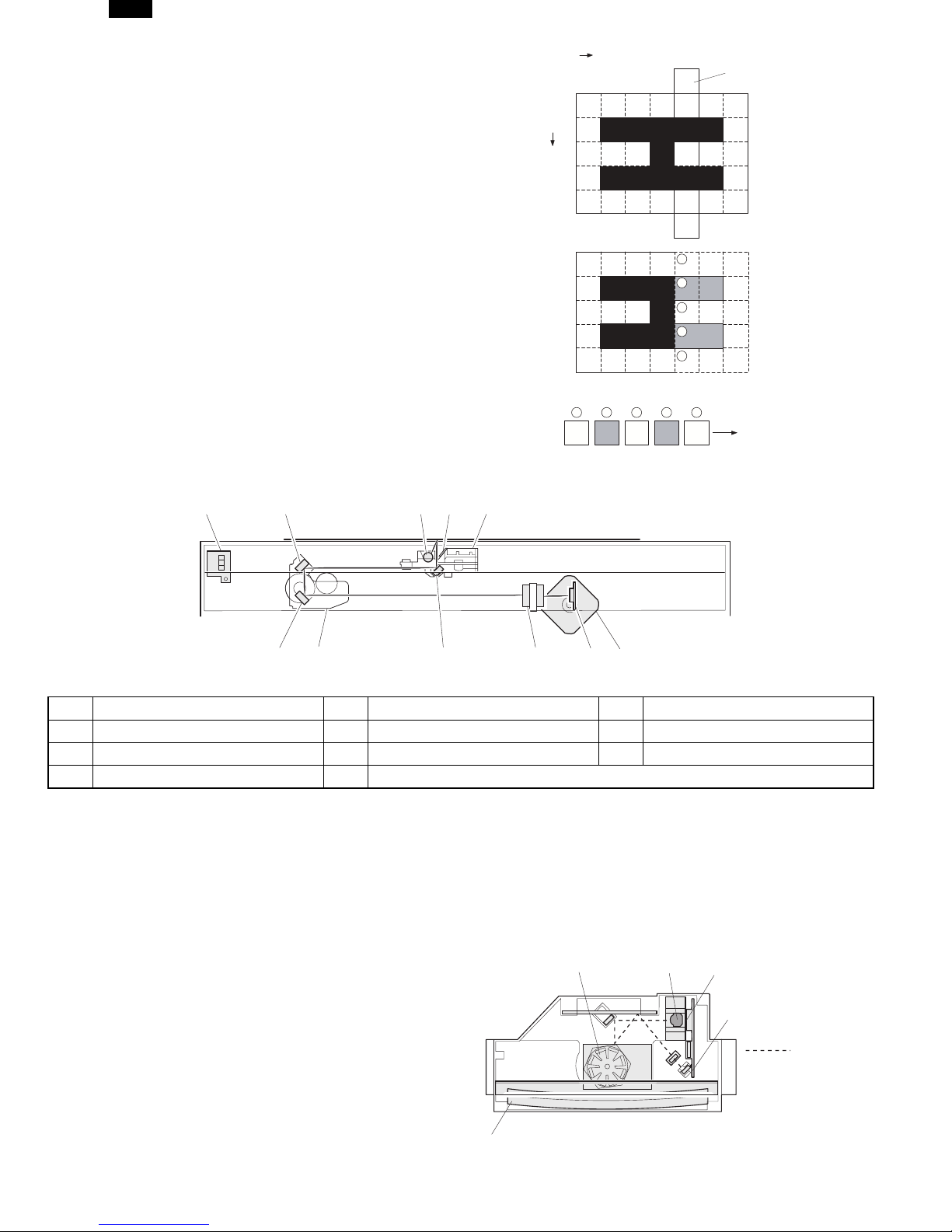
A.How to scan documents
The scanner has sensors that are arranged in a line. These sensors scan a
certain area of a document at a time and deliver outputs sequentially. When
the line is finished, the next line is scanned, and this procedure is repeated.
The figure below shows the case where the latter two sections of an image
which are scanned are shown with solid lines and the former two sections
which are being transmitted are shown with dotted lines.
The direction of this line is called “main scanning direction,” and the scanning
direction “sub scanning direction.”
In the figure above, one line is divided into 4 sections. Actually, however, one
line is divided into thousands of sections. For scanning, the light receiving element called CCD is used.
The basic resolution indicates the scanner capacity. The basic resolution is expressed in dpi (dot/inch) which shows the number of light emitting elements per
inch on the document.
The basic resolution of this machine is 400dpi.
In the sub scanning direction, at the same time, the motor that drives the optical system is controlled to scan the image at the basic resolution.
Sub scanning direction
Sensor scanning area
Main
scanning
direction
Original
1
2
3
4
5
Image data sent to the ICU PWB
5 4 3 2
1
To MCU PWB
B.Basic structure of scanner section
(1)
(11)
(4)
(7)
1Copy lamp (Xenon lamp)2Reflector (light conversion plate)3No. 1 mirror
4No. 2 mirror5No. 3 mirror6Lens
7No. 2/3 mirror unit8Copy lamp unit9CCD
10Mirror motor11MHPS (Mirror home position sensor)
The scanner unit performs scanning in the digital optical system.
The light from the light source (Xenon lamp) is reflected by a document and passed through three mirrors and reduction lenses to the CCD element
(image sensor) where images are formed. This system is known as the reduction image sensor system. Photo energy on the CCD element is converted into electrical signals (analog signals). (Photo-electric conversion). The output signals (analog signals) are converted into digital signals (A/D
conversion) and passed to the MCU (main control/image process section). The resolution at that time is 400dpi.
The mirror unit in the scanner section is driven by the mirror motor.
The MHPS is provided to detect the home position of the copy lamp unit.
(2)
(3)
(8)
(6)(5)
(9)
(10)
3.Laser unit
The image data sent from the MCU (image process circuit) is sent to
the LSU (laser unit), where it is converted into laser beams.
A.Basic structure
The LSU unit is the writing section of the digital optical system.
The semiconductor laser is used as the light source, and images are
formed on the OPC drum by the polygon mirror and fθ lens, etc.
The laser beams are passed through the collimator lens, the cylindrical
lens, the polygon mirror, the fθ lens, and the mirror to form images on
the OPC drum in the main scanning direction. The laser emitting PWB
is provided with the APC (auto power control) in order to eliminate fluctuations in the laser power. The BF PWB works for measurement of the
laser writing start point.
7 – 2
(3)
(5)
(1)(2)
(4)
: Laser beam
path for BF PWB
DP1200/1500
No.ComponentFunction
(1)Semiconductor laserGenerates laser beams.
(2)Collimator lens
Polygon mirror,
(3)
polygon motor
BD (Mirror, lens,
(4)
PWB)
(5)fθ lens
Makes the laser scanning speeds at both ends of the drum same as
each other.
a ≠ b ≠ c
abc
Converges laser beams in
parallel.
Reflects laser beams at a
constant rpm.
Detects start timing of laser
scanning.
Converges laser beams at a
spot on the drum.
Makes the laser scanning
speeds at both ends of the
drum same as each other.
(Refer to the figure below.)
d = e = f
def
4.Fuser section
A.General description
General block diagram (cross section)
Thermal fuse
Separator pawl
PPD2
f
θ
LENS
B.Laser beam path
C.Composition
Effective scanning width:216mm (max.)
Resolution:600dpi
Beam diameter:75um in the main scanning
direction, 80um in the sub scanning
direction
Image surface power:
Polygon motor section:
0.20 ±0.03mW (Laser wavelength
780 – 795nm)
Brushless motor 20.787rpm
No. of mirror surfaces: 6 surfaces
Thermistor
Pressure roller
Heat roller
Paper guide
Top view
Heat roller
(1)Heat roller
A Teflon roller is used for the heat roller and a silicone rubber roller is
used for the lower heat roller for better toner fusing performance and
paper separation.
(2)Separator pawl
Three separator pawls are used on the upper heat roller. The separator
pawls are teflon coated to reduce friction with the roller and prevent a
smear on the paper caused by the separator pawl.
Thermistor
Separator pawl
Thermal fuse
Heater lamp
7 – 3
DP1200/1500
(3)Thermal control
1.The heater lamp, thermistor, main PWB, DC power supply PWB,
and triac within the power supply unit are used to control the
temperature in the fuser unit.
To prevent against abnormally high temperature in the fuser unit, a
thermal breaker and thermal fuse are used for safety purposes.
Heated by the heater
lamp.(950W)
Saftey device
(Thermal breaker, thermal
fuse)
Triac (in the
power supply unit)
The surface temperature
of the upper heat roller is
sensed by the thermistor.
Level of the thermistor is
controlled by the main PWB.
With the signal from the
main PWB, the triac is
controlled on and off.
(power supply PWB)
2.The surface temperature of the upper heat roller is set to 165˚C ∼
190˚C. The surface temperature during the power save mode is set
to 100˚C.
3.The self-check function comes active when one of the following
malfunctions occurs, and an "H" is displayed on the multicopy window.
a.When the heat roller surface temperature rises above 240˚C.
b.When the heat roller surface temperature drops below 100˚C
during the copy cycle.
c.Open thermistor
d.Open thermal fuse
e.When the heat roller temperature does not reach 190˚C within
27 second after supplying the power.
(4)Fusing resistor
Fusing resistor
This model is provided with a fusing resistor in the fusing section to improve transfer efficiency.
General descriptions are made in the following.
General descriptions
Since the upper heat roller is conductive when copy paper is highly
moist and the distance between the transfer unit and the fusing unit is
short, the transfer current leaks through the copy paper, the upper heat
roller and the discharging brush.
5.Paper feed section and paper transport section
A.Paper transport path and general operations
(2)
(1)
(1)Scanner unit(6)Main charger(11)Pickup roller
(2)Copy lamp(7)Heat roller(12)Manual paper feed tray
(3)Lens unit(8)Pressure roller(13)Manual paper feed roller
(4)LSU (Laser unit)(9)Drum(14)PS roller unit
(5)Paper exit roller(10)Transfer unit(15)Paper feed roller
Paper feed is made in two ways; the tray paper feed and the manual paper feed. The tray is of universal-type, and has the capacity of 250 sheets.
The front loading system allow you to install or remove the tray from the front cabinet.
The general descriptions on the tray paper feed and the manual paper feed are given below.
(5)
(3)
(4)
(6)
(15)
(13)
(14)
(7)
(8)
(9)
(10)
(11)
(12)
7 – 4
DP1200/1500
(1)Cassette paper feed operation
1)The figure below shows the positions of the pick-up roller, the paper
feed clutch sleeve, and the paper feed latch in the initial state
without pressing the COPY button after lighting the ready lamp.
The paper feed latch is in contact with the projection of the clutch
sleeve.
2)When the COPY button is pressed, the main drive motor starts
rotating to drive each drive gear.
The pick-up drive gear also is driven at that time. Since, however,
the paper feed latch is in contact with the projection of the clutch
sleeve, rotation of the drive gear is not transmitted to the pick-up
roller, which does not rotate.
PFS
RRS
OFF
OFF
5)At this time, the paper is fed past the paper entry detection switch
(PPD1), and detected by it. After about 0.15 sec from detection of
paper by PPD1, the tray paper feed solenoid (PFS) turns on so that
the clutch sleeve projection comes into contact with the paper feed
latch to stop the pick-up roller. Then the pick-up roller rotates for
about 0.15 sec so that the lead edge of the paper is evenly pressed
on the resist roller, preventing against skew feeding.
PFS
RRS
ON
OFF
3)After about 0.1 sec from when the main motor start rotating, the
tray paper feed solenoid (PFS) turns on momentarily.
This disengages the paper feed latch from the projection of the
clutch sleeve, transmitting rotation of the pick-up drive gear to the
paper feed roller shaft, rotating the pick-up roller to feed the paper.
PFS
RRS
OFF
OFF
6)To release the resist roller, the tray paper feed solenoid and the
resist solenoid are turned on by the paper start signal to disengage
the resist start latch from the clutch sleeve projection, transmitting
rotation of the resist drive gear to the resist roller shaft. Thus the
paper is transported by the resist roller.
7)After the resist roller starts rotating, the paper is passed through the
pre-transfer guide to the transfer section. Images are transferred on
the paper, which is separated from the OPC drum by the drum
curve and the separation section.
PFS
RRS
OFF
ON
4)After more than half rotation of the pick-up roller, the paper feed
latch is brought in contact with the projection of the clutch sleeve,
stopping rotation of the pick-up roller.
8)The paper separated from the drum is passed through the fusing
paper guide, the heat roller (fusing section), POD (paper out detector) to the copy tray.
7 – 5

DP1200/1500
(2)Manual multi paper feed operation
1)Before paper feed operation, the manual paper feed solenoid
(MPFS) is turned OFF as shown in the figure below.
A
C
OF
F
MPFS
2)When the PRINT button is pressed, the manual paper feed
solenoid (MPFS) turns on to disengage the manual paper feed latch
A from the manual paper feed clutch sleeve A, rotating the manual
paper feed roller and the manual take-up roller. At the same time,
the manual paper feed stopper opens and the manual take-up roller
is pressed to the surface of the paper to start paper feeding.
3)When pawl C of the manual paper feed clutch sleeve is hung on the
manual feed latch, the manual feed stopper falls and the manual
take-up roller rises. At that time, the manual paper feed roller is
rotating.
A
C
ON
MPFS
4)The lead edge of the transported paper is pressed on the resist
roller by the transport roller. Then the paper is stopped temporarily
to make synchronization with the lead edge of the image on the
OPC drum.
The operations hereinafter are the same as the paper feed operations from the tray. (Refer to A-5 ∼ 8.)
ON
MPFS
5)The solenoid turns off to close the gate and return to the initial
state.
C
A
A
C
OF
F
MPFS
7 – 6

(3)Conditions of occurrence of paper misfeed
a.When the power is turned on:
PPD or POD is ON when the power is turned on.
b.Copy operation
a.PPD1 jam1)PPD1 does not turn off within 4 sec
after turning on the resist roller.
b.PPD2 jam1)PPD2 is off immediately after turning on
the resist roller.
2)PPD2 does not turn off within 1.2 sec
after turning off the resist roller.
c.POD jam1)POD does not turn on within 2.9 sec
after turning on the resist roller.
2)POD does not turn off within 1.5 sec
2.7 sec after turning off PPD2.
DP1200/1500
6. Printing process
(1) Functional diagram
(Basic operation cycle)
An OPC drum is used for the photoconductor.
(Structure of the OPC drum layers)
Main charger
Laser beam
MG roller
Cleaning blade
Semiconductor laser
OPC layer
(20microns thick)
Pigment layer
(0.2 to 0.3 microns thick)
Aluminium drum
Drum
Transfer unit
Resist roller
Focus correction lens
Main high voltage unit
Saw tooth
Cleaning blade
Waste toner box
To face
down tray
Paper release Fusing
Heat roller
Heater lamp
Cleaning
Separation
Electrode
Charge
7 – 7
Exposure
Drum
Transfer
Transfer charger
Transfer high
voltage unit
Developing
Cassette
paper feed
Synchronization
with drum
Toner
Developer
PS roller
Manual feed
Print process
Paper transport route

DP1200/1500
(2)Outline of print process
This printer is a non-impact printer that uses a semiconductor
laser and electrostatic print process. This printer uses an OPC
(Organic Photo Conductor) for its photoconductive material.
First, voltage from the main corona unit charges the drum surface and a latent image is formed on the drum surface using a
laser beam. This latent image forms a visible image on the
drum surface when toner is applied. The toner image is then
transferred onto the print paper by the transfer corona and
fused on the print paper in the fusing section with a combination of heat and pressure.
Step-1: Charge
Step-2:Exposure
∗ Latent image is formed on the drum.
Step-3: Developing
Latent image formed on the drum is then changed
into visible image with toner.
Step-4: Transfer
The visible image (toner image) on the drum is transfered onto the print paper.
Step-5: Cleaning
Residual toner on the drum surface is removed and
collected by the cleaning blade.
Step-6: Optical discharge
Residual charge on the drum surface is removed, by
semiconductor laser beam.
Semiconductor laser
Exposure
(semiconductor laser)
Drum surface charge
sfter the exposure
Non-image area Image area
OPC layer
Pigment
layer
Aluminum
drum
OPC layer
Pigment
layer
Aluminum
layer
(3)Actual print process
Step-1: DC charge
A uniform negative charge is applied over the OPC drum surface by the main charging unit. Stable potential is maintained
by means of the Scorotron charger.
Positive charges are generated in the aluminum layer.
About
DC5.5KV
(–580V/–400V)
Step-3: Developing (DC bias)
A bias potential is applied to the MG roller in the two component magnetic brush developing method, and the toner is
charged negative through friction with the carrier.
Non-image area of the drum surface charged with negative
potential repel the toner, whereas the laser exposed portions
where no negative charges exist, attract the toner. As a result,
a visible image appears on the drum surface.
: Carrier (Magnetized particle)
: Toner (Charge negative by friction)
(N) (S) :Permanent magnet
(provided in three locations)
N
S
N
Step-2: Exposure (laser beam, lens)
A Laser beam is generated from the semiconductor laser and
controlled by the print pattern signal. The laser writes onto the
OPC drum surface through the polygon mirrors and lens. The
resistance of the OPC layer decreases for an area exposed by
the laser beam (corresponding to the print pattern signal). The
beam neutralizes the negative charge. An electrostatic latent
image is formed on the drum surface.
7 – 8
DC
–400V ± 8V
MG roller

DP1200/1500
Non-image area
-600
Drum surface potential
-400
Developing bias
Image area
Residual potential (-50 to -100V)
0
Charge Exposure Developing Transfer
Toner at tract
potential
Time
Charge
Discharge
Toner is attracted over the shadowed area because of the
developing bias.
Step-4: Transfer
The visible image on the drum surface is transferred onto the
print paper by applying a positive charge from the transfer
corona to the backside of the print paper.
Step-7: Optical discharge (Semiconductor laser)
Before the drum rotation is stopped, the semiconductor laser is
radiated onto the drum to reduce the electrical resistance in the
OPC layer and elimate residual charge, providing a uniform
state to the drum surface for the next page to be printed.
When the electrical resistance is reduced, positive charges on
the aluminum layer are moved and neutralized with negative
charges on the OPC layer.
Semiconductor l aser
Charge by the Scorotron charger
Function
The Scorotron charger functions to maintain the surface potential of the drum even at all times which. It is used to control the
surface potential regardless of the charge characteristics of the
photoconductor.
Basic function
A screen grid is placed between the saw tooth and the
photoconductor. A stable voltage is added to the screen grid to
maintain the corona current on the photoconductor.
As the photoconductor is charged by the saw tooth from the
main corona unit, the surface potential increases. This increases the current flowing through the screen grid. When the
photoconductor potential nears the grid potential, the current
turns to flow to the grid so that the photoconductor potential can
be maintained at a stable level.
About DC 5.2kV
Step-5: Separation
Since the print paper is charged positively by the transfer
corona, it is discharged by the separation corona. The separation corona is connected to ground.
Step-6: Cleaning
Toner remaining on the drum is removed and collected by the
cleaning blade. It is transported to the waste toner collecting
section in the cleaning unit by the waste toner transport roller.
Process controlling
Function
The print pattern signal is converted into an invisible image by
the semiconductor laser using negative to positive (reversible)
developing method. Therefore, if the developing bias is added
before the drum is charged, toner is attracted onto the drum. If
the developing bias is not added when the drum is charged, the
carrier is attracted to the drum because of the strong electrostatic force of the drum.
To avoid this, the process is controlled by adjusting the drum
potential and the grid potential of the Scorotron charger.
Basic function
Voltage added to the screen grid can be selected, high and low.
To make it easily understood, the figure below shows voltage
transition at the developer unit.
START STOP
0
Toner attract
potenti al
2)
3)
1)
Low
4)
High
Print potentioal
Developing bias
Drum potential
Time
7 – 9

DP1200/1500
Start
1) Because the grid potential is at a low level, the drum potential is at about –400V. (Carrier may not be attracted though
the carrier is pulled towards the drum by the electrostatic
force of –400V.
2) Developing bias ( –400V) is applied when the photoconductor potential is switched from LOW to HIGH.
3) Once developing bias (–400V) is applied and the photo conductor potential rises to HIGH, toner will not be attracted to
the drum.
Stop
The reverse sequence takes place.
Retaining developing bias at an abnormal occurrence
Function
The developing bias will be lost if the power supply was
removed during print process. In this event, the drum potential
slightly abates and the carrier makes deposits on the drum because of strong static power. To prevent this, the machine incorporates a function to retain the developing bias for a certain
period and decrease the voltage gradually against possible
power loss.
Basic function
Normally, the developing bias voltage is retained for a certain
time before the drum comes to a complete stop if the machine
should stop before completing the normal print cycle. The
developing bias can be added before resuming the operation
after an abnormal interruption. Therfore, carrier will not make a
deposit on the drum surface.
7 – 10

DP1200/1500
[8]DISASSEMBLY AND ASSEMBLY
Before disassembly, be sure to disconnect the power cord for safety.
The disassembly and assembly procedures are described for the following sections:
1.High voltage section
2.Operation panel section
3.Optical section
4.Fusing section
5.Tray paper feed/transport section
6.Manual paper feed section
7.Rear frame section
8.Power section
9.SPF section
10.2nd cassette section
11.DUP motor section
12.Reverse roller section
13.FAX MCU PWB section
14.FAX-SPF section
1.High voltage section
A.List
No.Part name Ref.
1Drum
2Transfer charger unit
3Charger wire
B.Drum replacement
1)Remove the drum cover. (4 Lock Tabs)
2)Remove the drum fixing plate and the photoconductor drum.
(Note)Dispose the drum fixing plate which was removed.
L
O
C
K
(2)
(3)
3)Check the cleaning blade and the red felt for no damage.
•If there is any damage, execute all procedures from item 5) and
later.
•If there is no damage, execute the procedure of item 12).
4)Remove the main charger.
(Cleaning the screen grid and the sawteeth.)
8 – 1

DP1200/1500
5)Remove the cleaning blade.
Note:Dispose the cleaning blade which was removed.
6)Clean the cleaning section and the waste toner pipe to remove
waste toner completely with a vacuum cleaner.
7)Remove the felt and duplex tape completely.
Note:Be careful not to scratch or bend the sub blade.
8)Attach the cleaning blade.
Securely insert the plate section of the cleaning blade into the unit
and fix it with a screw.
Do not touch the cleaning blade rubber with your hand.
When attaching the cleaning blade, press the cleaning blade in the
arrow direction and attach.
Attach the mocket with slightly pressing section A of the cleaning blade.
Do not touch the tip of the cleaning blade.
Do not put the mocket under the cleaning blade.
Do not put the mocket on the sub blade.
Do not press the sub blade with the mocket.
10)Attach the main charger.
Securely set the MC holder on the projection of the process frame.
Securely insert two projections of the MC holder into the groove
in the process frame.
When attaching the MC holder ass’y, be careful not to make contact with the cleaning blade.
11)Attach the drum fixing plate and the photoconductor drum.
Apply grease to the inside of the photoconductor drum. (Dia. 2)
9)Attach the felt.
Attach the drum from (b). (Prevention against the sub blade edge
breakage)
Attach the drum so that its position with the sub blade is as shown.
8 – 2

DP1200/1500
12)Attach the detection gear.
Note:
•The detection gear is not installed to the drum cartridge packed
with the main body. Add a new one.
13)Attach the drum cover.
Note:After attaching the drum cover, do not make a copy.
When attaching the drum cover, engage the detection gear
20T rib with the 30T gear rib, and attach the drum cover to
the process frame.
C.Disassembly procedure
(1)Press the side cover open/close button and open the side cover.
(2)Push up the lock pawls (2 positions) of the side cover, and remove
the transfer charger.
Lock pawl rear
1)
2)
Transfer
charger
1)
Lock pawl front
D.Assembly procedure
1)
2)
For assembly, reverse the disassembly procedure.
E.Charger wire cleaning
(1)Remove the charger cleaner from the manual paper feed unit.
1)
8 – 3

DP1200/1500
(2)Set the charger cleaner to the transfer unit, and move it reciprocal-
ly a few times in the arrow direction shown in the figure below.
3)
4)
2)
1)
F.Charger wire replacement
(1)Remove the TC cover and remove the screw.
(2)Remove the spring and remove the charger wire.
(3)Install a new charger wire by reversing the procedures (1) and (2).
At that time, be careful of the following items.
●
The rest of the charger wire must be within 1.5mm.
●
The spring hook section (charger wire winding section) must be
in the range of the projection section.
●
Be careful not to twist the charger wire.
2.Operation panel section
A.List
No.Part name Ref.
1Operation panel unit
2Operation PWB
B.Disassembly procedure
(1)Remove the screws (4 pcs.), the harness, and the operation panel
unit.
1)
1)
2)
3)
1)
(2)Remove the screws (3 pcs.) and the PWB holder.
(3)Remove the screws (3 pcs.) and the operation PWB.
1)
Charger wire
Protrusion
1mm
1)
3)
1)
3)
2)
2)
3)
3)
4)
1.5mm
Note that there are 13 pawls
8 – 4

DP1200/1500
C.Assembly procedure
For assembly, reverse the disassembly procedure
3.Optical section
A.List
NO.Part name Ref.
1Copy lamp unit
2Copy lamp
3Lens unit
B.Disassembly procedure
(1)Remove the parts as shown below.
1)
(2)Remove the screws (2pcs.), and remove the copy lamp unit from
the mirror base drive wire.
2)
3)
1)
2)
3)
1)
2)
Hook
9)
7)
(3)Pull the copy lamp unit toward you to remove the harness.
4)
4)
10)
6)
3)
4)
5)
8)
2)
3)
1)
1)
3)
2)
(4)Remove the screw (4 pc) and remove the cover.
8 – 5

DP1200/1500
(5)Remove the screws (2 pcs.), the harness, and the optical unit.
1)
4)
3)
2)
5)
4.Fusing section
A.List
No.Part name Ref.
1Thermistor
2PPD2 sensor
3Heater lamp
4Pressure roller
5Heat roller
B.Disassembly procedure
(1)Remove the connectors (3 pcs.) of the rear cabinet.
(2)Open the side cover, remove two screws, and remove the fusing
unit.
When installing the lens unit, refer to “8-6. Lens unit installation reference.”
C.Assembly procedure
Basically reverse the disassembly procedure.
The mirror base drive wire and the lens drive wire stretching methods
are described below.
a.Mirror base drive wire stretching
1.Hook the metal fixture of the mirror base drive wire on the
projection of the optical base plate.
2.Pass the wire through the external groove of the double pulley.
(At that time, check that No. 2/3 mirror unit is in contact with the
mirror base positioning plate.)
3.Hold so that the winding pulley groove is up, and wind the mirror
base drive wire 9 turns.
4.Put the 8th turn of the mirror base drive wire in the winding pulley groove and fix with a screw.
5.Pass the wire under No. 2/3 mirror unit plate and wind it around
pulley A.
6.Pass the wire through the internal groove of the double pulley,
and pass through pulley B.
7.Hook the spring hook on the optical base plate.
6
6
5
5
7
7
7
7
6
6
5
5
2
2
6
6
6
6
6
6
2
2
6
6
1
1
1
1
3
3
Wind closely
Wind closely
2
2
Wind closely
Wind closely
3
3
1)
3)
2)
2)
(3)Cut the binding band, remove the screw, and remove the thermis-
tor.
1)
2)
2
2
After installing the mirror base drive wire, be sure to perform main
scanning direction image distortion adjustment.
4
4
Thermistor
3)
8 – 6

DP1200/1500
(4) Remove the screw and remove the U-turn guide.
1)
2)
Pressure roller section disassembly
(5) Remove the three screws, remove the fusing cover lower on the
right side, and open the heat roller section.
2)
3)
4)
6)
(7)Remove the plate spring on the right and remove the heater lamp.
1)
2)
Hearter lamp
(8)Remove the spring and remove the separation pawls (3 pcs.).
3)
5)
6)
5)
(6)Remove the screw and remove the PPD2 sensor.
1)
2)
PPD2 sensor
1)
2)
1)
(9)Remove the E-ring and remove the reverse gate.
3)
1)
2)
8 – 7

DP1200/1500
(10)Remove the pressure release levers on the right and the left
sides.
1)
1)
(11)Remove the pressure roller, the pressure bearing, and the spring.
Note:Apply grease to the sections specified with ✽.
✽
Pressure roller
(6)Remove the C-ring and the fusing bearing, and remove the heat
roller.
1)
2)
3)
(7)Remove the parts from the heat roller.
Note:Apply grease to the sections specified with ✽.
✽
Heat roller
1)
3)
2)
✽
1)
2)
3)
Heat roller disassembly
(Continued from procedure (4).)
(5)Remove screws, remove the fusing cover, and open the heat roller
section.
3)
✽
3)
(8)Remove two screws and remove the thermostat.
1)
2)
1)
2)
2)
2)
1)
3)
3)
C.Assembly procedure
For assembly, reverse the disassembly procedure.
8 – 8

DP1200/1500
5.Tray paper feed/transport section
A.List
No.Part name Ref.
1PPD1 sensor PWB
2LSU unit
3Intermediate frame unit
4Paper feed roller
B.Disassembly procedure
(1)Remove six connectors and screws of the main PWB, and lift the
optical unit and the main PWB to remove.
2)
2)
2)
2)
(3)Remove two screws and remove the toner motor.
2)
1)
(4)Remove two springs and open the intermediate frame unit.
3)
1)
1)
(2)Remove the PWB insulation mylar and remove the paper transport
detection sensor (PPD2).
2)
1)
2)
1)
3)
8 – 9

DP1200/1500
(5)Remove the pulleys on the both sides and remove the paper exit
roller.
3)
1)
4)
2)
(7)Release the belt pulley lock and remove the belt pulley bearing.
3)
2)
1)
(6)Pull out the paper exit roller knob and remove the belt.
2)
(8)Remove the paper exit roller.
1)
8 – 10

DP1200/1500
(9)Remove the harness guide.
(10)Remove five screws and remove the main drive plate and the
belt.
2)
(11)Remove the parts as shown below, and remove the pressure
release solenoid and the paper feed solenoid.
3)
4)
2)
1)
1)
4)
2)
3)
1)
(12)Remove six screws and remove the LSU unit.
2)
1)
3)
1)
1)
CAUTION:Attach
the gears
securely
8 – 11

DP1200/1500
(13)Remove two screws and remove the fusing connector.
(14)Remove five screws and the connector, and lift the intermediate
frame unit to remove.
3)
4)
2)
2)
(17)Remove three screws and remove the TC front paper guide.
1)
2)
(18)Remove the screw and the connector, and remove the PPD1
sensor PWB.
1)
(15)Remove the screw and the E-ring, and remove the PS semi-cir-
cular earth plate and the PS roller unit.
(16)Remove the E-ring and remove the spring clutch from the PS
roller unit.
5)
5)
4)
4)
PS roller unit
PS roller unit
4)
4)
PS semi-circuler
PS semi-circuler
earth plate
earth plate
1)
1)
1)
2)
2)
2)
3)
3)
8 – 12

DP1200/1500
(19)Remove two E-rings and remove the paper feed roller.
(20)Remove three E-rings and remove the clutch unit.
5)
Clutch unit
Paper feed
roller
4)
3)
1)
Back
4)
Front
6. Manual paper feed section
A.List
No.Part name Ref.
1Manual transport roller
2Cassette detection switch
3PPD1 sensor PWB
4Side door detection unit
B.Disassembly procedure
Single unit
(1)Remove the screw and remove the single upper cover.
1)
2)
C.Assembly procedure
For assembly, reverse the disassembly procedure.
2)
8 – 13

DP1200/1500
(2)Remove the screw and remove the side door detection unit.
2)
1)
Back
(3)Remove three screws and remove the single manual feed upper
frame.
Wire treatment
(4)Remove the PPD1 sensor PWB.
1)
3)
2)
1)
Wire treatment
1)
(5)Remove the E-ring and remove the manual paper feed transport
roller.
2)
3)
4)
3)
1)
2)
8 – 14

DP1200/1500
(6)Remove the cassette detection switch.
1)
3)
2)
Multi unit
(1)Remove the screw and remove the multi upper cover.
1)
3)
2)
Wire treatment
(7)Remove the multi cover.
Multi cover
(2)Remove the screw and remove the side door detection unit.
Orange
Red
1)
2)
1)
Back
Wire treatment
8 – 15

DP1200/1500
(3)Remove three screws and remove the multi paper feed upper
frame.
1)
1)
2)
(5)Remove three E-rings and remove the manual paper feed roller.
1)
1)
1)
2)
3)
O
C
L
K
T
O
K
(4)Remove two screws and remove the multi feed bracket unit from
the multi paper feed upper frame.
2)
1)
1)
2)
(6)Remove the pick-up roller.
1)
2)
8 – 16

DP1200/1500
(7)Cut the binding band and remove the multi paper feed solenoid.
1)
Multi paper feed
solnoid
3)
2)
7.Rear frame section
A.List
No.Part name Ref.
1Mirror motor
2Main motor
3Exhaust fan motor
B.Disassembly procedure
(1)Remove three screws and remove the rear cabinet.
1)
1)
2)
C.Assembly procedure
For assembly, reverse the disassembly procedure.
D.Pressure plate holder attachment
(1)Attach the pressure plate holder so that the resin section is not
covered with the seal M1-N.
Seal M1-N
Pressure plate
holder
Attachment
reference
Attachment
reference
1)
(2)Remove two screws, the harness, and the mirror motor.
3)
1)
2)
2)
8 – 17

DP1200/1500
(3)Remove two screws and one harness, and remove the main
motor.
3)
1)
2)
8.Power section
A.List
No.Part name Ref.
1Power PWB
B.Disassembly procedure
(1)Remove two screws and one connector, and remove the power
PWB.
2)
3)
2)
1)
(4)Remove two screws and one connector, and remove the exhaust
fan motor.
1)
3)
C.Assembly procedure
For assembly, reverse the disassembly procedure.
C.Assembly procedure
For assembly, reverse the disassembly procedure.
8 – 18

DP1200/1500
[9]ADJUSTMENTS
1.Optical section
A.Image distortion adjustment
There are following two types of image distortion.
●
Horizontal image distortion
●
Vertical image distortion
In this machine, the image distortion is adjusted by changing the parallelism of mirrors (copy lamp unit, No. 2/3 mirror unit).
(1)Horizontal image distortion adjustment
a.Summary
Parallelism of mirrors can be made by installing the copy lamp unit
and No. 2/3 mirror unit to the reference position. However, it must
be checked by making a copy, and must be adjusted if necessary.
b.Cases when the adjustment is required
1)When the copy lamp unit and No.2/3 mirror unit are disassembled or their part is replaced.
2)When the copy lamp unit and No.2/3 mirror unit drive section is
disassembled or its part is replaced.
3)When the copy image is distorted as shown below:
Document
Copy A
Copy B
d.Adjustment procedure
1)Remove the right cabinet (manual paper feed unit), the document reference plate.
2)Remove the document glass.
1)
2)
3)
3)Loosen the fixing screw of the copy lamp unit wire.
c.Necessary tools
●
Screwdriver (+)
●
Hex wrench
●
Scale
●
Test chart for distortion adjustment (Make a chart shown below
by yourself.)
Draw a rectangle on a paper (B4 or 8 1/2″ × 14″) as shown
below.
Be sure to make four right angles.
L
L
L
L
L = 10mm
Fixing Screws
4)Manually turn the copy lamp unit/No.2/3 mirror unit drive gear to
bring No.2/3 mirror unit into contact with No.2/3 mirror unit
positioning plate. When No.2/3 mirror unit makes contact with
No.2/3 mirror unit positioning plate in the Freat and rear frame
side simultaneously, the mechanical parallelism of No.2/3 mirror
unit is proper.
If one side of No.2/3 mirror unit makes contact with No.2/3 mirror
unit positioning plate and the other side does not, the parallelism
is improper.
If the parallelism is improper, perform the procedure of step 5).
9 – 1

5)Loosen the copy lamp unit/No.2/3 mirror unit drive pulley
setscrew in the side where No.2/3 mirror unit does not make
contact with No.2/3 mirror unit positioning plate.
DP1200/1500
7)Manually turn the copy lamp unit/No.2/3 mirror unit drive gear to
bring No.2/3 mirror unit into contact with the positioning plate,
and perform the procedure of step 4).
Repeat procedures of steps 4) to 7) until the parallelism of
No.2/3 mirror unit is properly set.
8)With No.2/3 mirror unit positioning plate in contact with No.2/3
mirror unit, bring the copy lamp unit into contact with the right
frame and fix the copy lamp unit to the drive wire.
Procedures 1) to 8) are for adjustment of mechanical horizontal
parallelism. The copy lamp unit and No.2/3 mirror are fixed to the
specified positions and the mechanical horizontal parallelism of
No.2/3 mirror is adjusted.
Then the optical horizontal parallelism must be adjusted in the
following procedures.
Copy lamp unit projection
Set screw
Scanner unit drive pulley
6)Without moving the copy lamp unit/No.2/3 mirror unit drive pulley
shaft, manually turn the copy lamp unit/No.2/3 mirror unit drive
pulley in the same direction of the loosened setscrew. When it
makes contact with No.2/3 mirror unit positioning plate, tighten
and fix the setscrew.
9)Set the image distortion check chart on the document table, and
make a reduction copy (75%) on an A4 or 11″ × 8 1/2″ paper
with the document cover open.
50mm
Image distortion check chart
9 – 2

DP1200/1500
10)Check the horizontal image distortion.
If LL = LR, there is no horizontal distortion
LL and LR: Distance between the copy
image horizontal line and
LL
the edge of the black
LR
background.
Black background
11)If LL is not equal to LR, perform the following procedure.
Loosen the setscrew of the copy lamp unit/No.2/3 mirror unit
drive pulley in the front or the rear frame.
Set screw
(2)Vertical image distortion adjustment
a.Summary
In this adjustment, the left and right balance is adjusted by changing
the left and right balance of the No. 2 scanner unit frame on the
front frame side.
b.Note
●
Horizontal image distortion adjustment
c.Cases when the adjustment is required
1)When the copy lamp unit/No.2/3 mirror unit drive section is disassembled or its part is replaced.
2)When the copy image is distorted as follows:
Document
Copy C
Copy D
d.Necessary tools
●
Screwdriver (+)
●
Screwdriver (–)
●
Scale
●
Test chart for distortion adjustment (Make by yourself.)
Draw a rectangle on A4 or 8 1/2″ × 11″ paper as shown below:
Be sure to make four right angles.
Scanner unit drive pulley
12)Without moving the copy lamp unit/No.2/3 mirror unit drive pulley shaft, manually turn the copy lamp unit/No.2/3 mirror unit
drive pulley whose setscrew was loosened, and adjust the
parallelism of copy lamp unit/No.2/3 mirror unit.
L
L
L
L = 10mm
L
e.Adjustment procedure
1)Set the test chart for image distortion adjustment on the document glass, and make a normal copy on a paper of A4 or 8 1/2″
× 11″.
2)Check image distortion in the right and the left sides.
If the both vertical lines are in parallel with each other, the rightleft distortion balance is proper. (However, there may be some
distortion.)
2)If all the four angles are right angles, there in no distortion and
the following procedures are not required.
Greater distortion
Smaller distortion
13)Tighten the set screw of the copy lamp unit/No.2/3 mirror unit
drive pulley.
14)Check the image distortion in the same manner as step 10).
Repeat procedures 11) to 14) until horizontal image distortion
is eliminated.
9 – 3

DP1200/1500
3)If the right-left distortion balance is improper, loosen the fixing
screw of No.2/3 mirror unit rail to change and adjust the right-left
balance of No.2/3 mirror unit rail.
(Note)
If the distortion in the lead edge side (when viewed in the paper
transport direction) is greater, change the height of the left rail of
No.2/3 mirror unit.
If the distortion in the rear edge side (when viewed in the paper
transport direction) is greater, change the height of the right rail
of No.2/3 mirror unit.
(1)Outline
The main scanning (front/rear) direction magnification ratio adjustment is made automatically or manually.
Automatic adjustment: The width of the reference line marked on
the shading correction plate is scanned to perform the main scanning (front/rear) direction magnification ratio adjustment automatically.
Manual adjustment: The adjustment is made by manual key operations. (In either of the automatic and manual adjustments, the zoom
data register set value is changed for adjustment.)
The magnification ratio in the sub scanning direction is adjusted by
changing the mirror base (scanner) scanning speed.
(2)Main scanning direction magnification ratio adjustment
a.Note
Before performing this adjustment, the following adjustments must
have been completed. If not, this adjustment cannot be performed
properly.
●
Image distortion adjustment
●
The lens unit must be installed in the reference position.
b.Cases when the adjustment is required
1)When the lens and the mirror unit are disassembled or the part
is replaced.
2)When the copy lamp unit/No.2/3 mirror unit drive section is disassembled or the part is replaced.
3)When the main PWB is replaced.
4)When the EEPROM in the main PWB is replaced.
5)When “U2” trouble occurs.
6)When the copy image distortion adjustment is performed.
Change the height of the right side of the rail.
Change the height of the left side of the rail.
4)Make a copy to check the vertical image distortion.
If the four angles are right angles, the adjustment is completed.
B.Copy magnification ratio adjustment
The copy magnification ratio must be adjusted in the main scanning
direction and in the sub scanning direction. To adjust, use SIM 48-1.
c.Necessary tools
●
Screwdriver (+)
●
Scale
d.Adjustment procedure
1)Set the scale vertically on the document table. (Use a long scale
for precise adjustment.)
2)Set the copy magnification ratio to 100%.
3)Make a copy on A4 or 81⁄2″ × 11″ paper.
9 – 4

DP1200/1500
4)Measure the length of the copied scale image.5)Calculate the main scanning direction magnification ratio.
Main scanning direction magnification ratio
Copy image dimensions
=
Original dimension
× 100 (%)
(When a 100mm scale is used as the original.)
Paper feed
direction
mm
1/2mm
mm
1/2mm
Reference
10
1020
20
6)Check that the copy magnification ratio is within the specified
range. If it is not within the specified range, perform the following
procedures.
7)Execute SIM 48-1 to select the main scanning direction copy
magnification ratio adjustment mode.
To select the adjustment mode, use the copy mode select key.
In the case of the automatic adjustment, when the PRINT switch is
pressed, the mirror base unit moves to the white plate for shading
to scan the width of the reference line, calculating the correction
value and displaying and storing this value.
After execution of the automatic adjustment, go out from the simulation mode and make a copy to check the magnification ratio.
If the magnification ratio is not in the specified range (100 ±1.0%),
manually adjust as follows.
Adjustment modeLighting lamp
Main scanning direction auto
copy magnification ratio
adjustment
Main scanning direction manual
copy magnification ratio
adjustment
Sub scanning direction copy
magnification ratio adjustment
Auto exposure lamp
ON
Manual exposure lamp
ON
Photo exposure lamp
ON
Original (Scale)
HARDDENCD
100110120 130
110
100
Comparison point
JAPAN
JAPAN
120 130
140
140
150
150
STAINLESS
Shizuoka
HARDDENCD
STAINLESS
Shizuoka
Copy
110
b.Cases when the adjustment is required
1)When the lens and the mirror unit are disassembled or the part
is replaced.
2)When the scanner unit drive section is disassembled or the part
is replaced.
3)When the main PWB is replaced.
4)When the EEPROM in the main PWB is replaced.
5)When “U2” trouble occurs.
6)When the copy image distortion adjustment is performed.
c.Necessary tools
●
Screwdriver (+)
●
Scale
d.Adjustment procedure
1)Set the scale on the document table as shown below. (Use a
long scale for precise adjustment.)
8)Set the adjustment mode to Manual with the copy mode select
key.
9)Enter the new set value of main scanning direction copy magnification ratio with the copy quantity set key, and press the
COPY button.
10)Change the set value and repeat the adjustment until the ratio
is within the speoified range.
When the set value is changed by 1, the magnification ratio is
changed by 0.1%.
(3)Sub scanning direction copy magnification ratio
a.Note
Before performing this adjustment, the following adjustments must
have been completed. If not, this adjustment cannot be performed
properly.
●
Image distortion adjustment
●
Must be installed to the lens unit reference position.
9 – 5
2)Set the copy magnification ratio to 100%.
3)Make a copy on A4 or 81⁄2″ × 11″ paper.
4)Measure the length of the copied scale image.
5)Calculate the sub scanning direction copy magnification ratio.
Sub scanning direction copy magnification ratio
Copy image dimension
=
Original dimension
× 100 (%)

mm
1/2mm
1020
100
110120 130
JAPAN
110
140
Original (Scale)
HARDDENCD
STAINLESS
150
Shizuoka
DP1200/1500
mm
1/2mm
Reference
10
20
100
Comparison point
6)Check that the actual copy magnification ratio is within the
specified range. (100 ± 1.0%).
If it is not within the specified range, perform the following procedures.
7)Execute SIM 48-1 to select the sub scanning direction copy
magnification ratio adjustment mode.
To select the adjustment mode, use the copy mode select key.
(Photo exposure lamp ON)
8)Enter the new set value of sub scanning direction copy magnification ratio with the copy quantity set key, and press the
COPY button.
Repeat procedures 1) — 8) until the sub scanning direction actual
copy magnification ratio in 100% copying is within the specified
range.
When the set value is changed by 1, the magnification ratio is
changed by 0.1%.
C.Lens unit attachment reference
Attach the lens unit so that the lens unit number on the lens adjustment
plate is aligned with the scribe line on the base plate.
Lens unit number
110120
Paper feed
direction
JAPAN
130
140
150
Copy
HARDDENCD
STAINLESS
Shizuoka
D.Image position adjustment
There are following five kinds of image position adjustments, which are
made by laser control except for the image scan start position adjustment. For the adjustments, SIM 50 – 01 and SIM 50 – 10 are used.
No.Adjustment itemSimulation
1Print start position50 – 01
2Image lead edge void amount50 – 01
3Image scan start position50 – 01
4Image rear edge void amount50 – 01
5Center offset50 – 10
To select the adjustment mode with SIM 50 – 01, use the copy density
select key.
The relationship between the adjustment modes and the lighting lamps
are as shown in the table below.
Adjustment modeLighting lamp
Print start positionAuto (AE) lamp
Image lead edge void amountManual (TEXT) lamp
Image scan start positionPhoto lamp
Image rear edge void amount
Auto, Manual, Photo
lamps
Example:Lens unit number –2.8
Attach the lens unit at 2 scales in the paper exit direction
from the reference line.
Note:Never touch the other screws than the unit attachment screw.
The lens unit is supplied only in a whole unit.
(–) direction
Reference line (0)
(+) direction
To select the adjustment mode with SIM 50 – 10, use the copy mode
select key.
The relationship between the adjustment modes and the lighting
lamps are as shown in the table below.
Machine with the multi manual paper feed unit
Adjustment modeLighting lamp
Print center offset (cassette)Auto, Cassette
Print center offset (manual feed)Auto, Manual
Document center offsetAuto, Manual
Machine with the single manual paper feed unit
Print center offset (cassette)Auto, Cassette
Print center offset (manual feed)Auto
Document center offsetAuto, Manual
9 – 6

DP1200/1500
(1)Lead edge adjustment
1)Set a scale to the center of the paper lead edge guide as shown
below, and cover it with B4 or 8 1/2″ × 14″ paper.
2)Execute SIM 50 – 01
3)Set the print start position (AE lamp ON) (A), the lead edge void
amount (TEXT lamp ON) (B), and the scan start position (PHOTO
lamp ON) (C) to 0, and make a copy of a scale at 100%.
4)Measure the image loss amount (R mm) of the scale image.
Set C = 10 × R (mm). (Example: Set the value of C to 30.)
When the value of C is increased by 10, the image loss is
decreased by 1mm. (Default: 50)
5)Measure the distance (H mm) between the paper lead edge and the
image print start position.
Set A = 10 × H (mm). (Example: Set the value of A to 50.)
When the value of A is increased by 10, the image lead edge is
shifted to the paper lead edge by 1mm. (Default: 50)
6)Set the lead edge void amount to B = 50 (2.5mm).
When the value of B is increased by 10, the void amount is increased by about 1mm. For 25 or less, however, the void amount
becomes zero. (Default: 50)
3)Make a copy and measure the void amount of image rear edge.
Void amount (Standard value: 2 – 3mm)
Scale image
Paper rear edge
4)If the measurement value is out of the specified range, change the
set value and repeat the adjustment procedure.
The default value is 50.
Note:The rear edge void cannot be checked with the first sheet
after entering the simulation mode, the first sheet after turning off/on the power, or the first sheet after inserting the cassette. Use the second or later sheet to check the rear edge
void.
(3)Center offset adjustment
1)Set the self-made test chart for the center position adjustment so
that its center line is aligned with the center mark of the document
guide.
●
Test chart for the center position adjustment
Draw a line at the center of A4 or 8 1/2″ × 11″ paper in the
paper transport direction.
(Example)
Distance between paper lead
edge and image: H = 5mm
Image loss:
R = 3mm
5mm
10mm
(2)Image rear edge void amount adjustment
1)Set a scale to the rear edge section of A4 or 11″ × 8 1/2″ paper size
as shown in the figure below, and cover it with B4 or 8 1/2″ × 14″
paper.
B4 or 8 1/2″ × 14″ paper
A4 size rear edge
Document guide
Center
Copy paper
(A4 or 8 1/2″ × 11″)
2)Execute SIM 50 – 10 to select the print center offset (cassette paper
feed) adjustment mode.
The set adjustment value is displayed on the copy quantity display.
3)Make a copy and check that the copied center line is properly positioned.
The standard value is 0 ± 2mm from the paper center.
(Copy A)
(Copy B)
2.0mm or less
Shift
2.0mm or less
Copy image
Copy paper
folding line
Copy image
2)Execute SIM 50 – 01 to select the image rear edge void amount adjustment mode.
The set adjustment value is displayed on the copy quantity display.
9 – 7
(Paper feed direction)
Shift
Copy paper
folding line

DP1200/1500
4)If the measured value is out of the specified range, change the set
value and repeat the adjustment procedure.
When the set value is increased by 1, the copy image is shifted by
0.1mm toward the rear frame.
l
For the manual paper feed, change the manual paper feed adjustment mode and perform the similar procedures.
l
Since the document center offset is automatically adjusted by
the CCD which scan the reference lines (F/R) on the back of
document guide, there is no need to adjust manually.
2.Copy density adjustment
A.Copy density adjustment timing
The copy density adjustment must be performed in the following cases:
l
When maintenance is performed.
l
When the developing bias/grid bias voltage is adjusted.
l
When the optical section is cleaned.
l
When a part in the optical section is replaced.
l
When the optical section is disassembled.
l
When the OPC drum is replaced.
l
When the main control PWB is replaced.
l
When the EEPROM on the main control PWB is replaced.
l
When the memory trouble (U2) occurs.
B.Note for copy density adjustment
1)Arrangement before execution of the copy density adjustment
l
Clean the optical section.
l
Clean or replace the charger wire.
l
Check that the voltage at the high voltage section and the developing bias voltage are in the specified range.
E.Copy density adjustment procedure
Use SIM 46-01 to set the copy density for each copy mode.
For selection of modes, use the copy mode select key.
(1)Test chart setting
1)Place the test chart so that its edge is aligned with the A4 (Letter)
reference line on the document table. Then place a B4 (14 8
1/2 ) white paper on the test chart and close the document cover.
White paper
Test chart
C.Necessary tool for copy density adjustment
l
TOSHIBA TEST CHART No.15-1.
l
B4 (14 8 1/2 ) white paper
l
The user program AE setting should be "3."
D.Features of copy density adjustment
For the copy density adjustment, the image data shift function provided
in the image process LSI is used.
List of the adjustment modes
Auto ModeBrightness 1 step only
Manual Mode
Photo Mode
Manual T/S
mode
T/S Auto modeBrightness 1 step only
Brightness 5 steps. Adjustment of only the
center brightness is made.
Brightness 5 steps. Adjustment of only the
center brightness is made.
Brightness 5 steps. Adjustment of only the
center brightness is made.
(2)Perform the adjustment in each mode.
1)Execute SIM 46-1.
2)Select the mode to be adjusted with the exposure mode select key.
(1)
(1)Mode select key/display
lamp
Adjustment
mode
Auto modeAuto lamp ON
Manual modeManual lamp ON
Photo modePhoto lamp ON
Manual T/S
mode
Auto T/S
mode
Exposure mode
display lamp
Manual lamp/Photo
lamp ON
Auto lamp/Photo
lamp ON
Gray chart
adjustment level
"S3" is slightly
copied.
"S3" is slightly
copied.
"S3" is slightly
copied.
"S4" is slightly
copied.
"S4" is slightly
copied.
9 — 8

DP1200/1500
3)Make a copy.
Check the adjustment level (shown in the above table) of the exposure test chart (Gray Scale).
(When too bright):Decrease the value displayed on the copy
quantity display.
(When too dark):Increase the value displayed on the copy quantity
display.
* The value can be set in the range of 1 – 99.
3.High voltage adjustment
A.Main charger (Grid bias)
Note:
Use a digital multi meter with internal resistance of 10M or
more measurement.
After adjusting the grid LOW output, adjust the HIGH output.
Do not reverse the sequence.
Procedures
1.Set the digital multi meter range to DC700V.
2.Set the positive side of the test rod to the connector CN11-3 (GRID)
of high voltage section of the power PWB and set the negative side
to the frame ground (radiating plate).
3.Execute SIM 8-3. (The main charger output is supplied for 30 sec
in the grid voltage LOW output mode.)
4.Adjust the control volume (VR-141) so that the output voltage is
400– ± 20V.
5.Execute SIM 8-2. (The main charger output is supplied for 30 sec
in the grid voltage HIGH output mode.)
6.Adjust the control volume (VR-142) so that the output voltage is 580
±10V.
B.DV bias adjustment
Note:
A digital multi meter with internal resistance of 1G must be
used for correct adjustment.
Procedures
1.Set the digital multi meter range to DC500V.
2.Set the positive side of the test rod to the connector CN-10-1 (DV
BIAS) and set the negative side to the connector CN10-2 (FG).
3.Execute SIM 8-1. (The developing bias is outputted for 30 sec.)
4.Adjust the control volume (VR-121) so that the output voltage is
–400 ± 5V.
9 — 9

[10] SIMULATION, TROUBLE CODES
1. Entering the simulation mode
To enter the serviceman simulation mode, press the keys as follows:
Clear Density select Clear Density select
To cancel the simulation mode, press the clear key.
Flow chart o entering the simulation mode
1
DP1200/1500
The current set adjustment
value and the counter
value are displayed on the
COPY QUANTITY
displayed Sensor check,
etc. are displayed by the
alarm lamps, etc.
To change the current set
values, enter with the COPY
QUANTITY key.
10th digit:
1st digit:
Count up of values:
COPY QUANTITY key
Count down of values:
Zoom key + COPY
QUANTITY key
The entered value
is displayed on the
COPY QUANTITY
display.
Press the COPY
key.
Is there a sub
code ?
NO
Press the COPY
key.
Is it the
simulation for
operation
check?
YES
Preform the operation
according to the
simulation number.
Is another
simulation to be
performed ?
NO
Press the clear key.
All displays on the
operation panel go off,
and the machine enters
the ready state for
entering the main code.
YES
YES
Press the COPY key.
The COPY QUANTITY
display blinks to indicate
"00" and the machine
enters the ready
state for sub code input.
Enter the sub code with
the COPY QUANTITY key.
10th digit:
1st digit:
Count up of values:
COPY QUANTITY key
Count down of values:
Zoom key + COPY
QUANTITY key
Press the COPY key.
Is the
main code the
same ?
NO
Is the
sub code
displayed ?
YES
Press the clear key.
The COPY QUANTITY
display blinks to indicate
the previously set sub
enters the ready7 state for
sub code input.
code, and the machine
YES
Press the clear key.
NO
Enter the new main
code.
The main code is
displayed on the
COPY QUANTITY
display.
Start
Press the clear key.
Within 1sec
Press the exposure
mode selector key.
Within 1sec
Press the clear key.
Within 1sec
Press the exposure
mode selector key.
All displays on the
operation panel go off,
and the machine enters
he ready state for entering
he main code.
Enter the main code with
the COPY QUANTITY key.
10th digit:
1st digit:
Count up of values:
COPY QUANTITY key
Count down of values:
Zoom key + COPY
QUANTITY key
The main code is
displayed on the
COPY QUANTITY
display.
The entered value
Press the clear key.
is registered.
End
1
10 – 1

2. List of simulations
Note: In the DP1200, simulations related to option units cannot be executed.
DP1200/1500
Sim
No.
01 Optical
02 SPF
05 Lamp ON
06 Machine
07 Aging 0106Warm up display and aging with
08 High
10 Other None Toner motor aging
14 Trouble
16 U2 trouble
20 Maintenance
21 Counter
22 Counter
24 Special
25 Main motor
Kind of
main code
system
Individual
load
operation
check
individual
load
operation
voltage
output check
reset
reset
counter
clear
setup
(When
maintenance)
display
counter
clear
ON
Sub
code
01 Mirror scan operation
02
SPF sensor status display
03
Motor ON
04
Paper feed solenoid ON
01
Operation panel display check
02
Fusing lamp ON + Cooling fan
HIGH/LOW speed
03
Copy lamp ON
0102Paper feed solenoid ON
Resist solenoid ON
jam
Intermittent aging
01
Developing bias (5V signal)
02
Main charger (Grid high)
03
Grid voltage (Low)
06
Transfer charger
None Cancel troubles other than U2
None Cancel of U2 trouble
01 Maintenance counter clear
01 Maintenance cycle setup
01
Maintenance counter display
02
Maintenance preset display
04
Jam total counter display
05
Total counter display
06
Developer counter display
08
SPF counter display
12
Drum counter display
14
P-ROM version display
17
Copy counter display
18
Printer counter display
21
Scanner counter display
22
SPF jam total counter display
01
Jam total counter clear
04
SPF counter clear
06
Developer counter clear
07
Drum counter clear
08
Copy counter clear
09
Printer counter clear
13
Scanner counter clear
14
SPF jam total counter clear
01
Developing bias
(High voltage output)
10
Polygon motor ON
Operation
Sim
No.
26 Various
30 Sensor
43 Fusing
46 Exposure
48 Magnification
50 Lead edge
51 Timing
61 Laser
63 Shading 01 Shading check
64 Self print 01 Self print only with the engine
67 Program
Kind of
main code
setup
operation
check
(Standard
provision)
temperature
setup
adjustment
ratio
correction
adjustment
adjustment
system
operation
Download
Sub
code
01
Manual feed setup
02
SPF setup
03
Second cassette setup
06
Destination setup
07
Machine conditions check
20
Rear edge void setup
30
CE mark conformity control
ON/OFF setup
37
Cancel of stop at developer over
39
Memory capacity setup
40
Polygon motor OFF time setup
42
Transfer ON timing control setup
43
Side void setup
44
SPF document rear edge read
setup
01 Paper sensor status display
01
Normal copy
04
Fusing temperature setup 2
09
Postcard size paper fusing control
setup
0119Copy density adjustment
Table adjustment (Copy mode)
01 Front/rear scan direction
0110Lead edge image position
adjustment
Paper lead edge/rear edge void
adjustment
Paper center offset +
OC/Document center offset +
SPF document center offset
0206Resist quantity adjustment
SPF exposure correction
03 Polygon motor check
(HSYNC output check)
(1 by 2 mode)
14 PCL PWB program download
Operation
10 – 2

DP1200/1500
3.Contents of simulations
Input method: Clear key Exposure Select key Clear key Exposure Select key
Main codeSub code Content
0101Mirror scan operation
(Operation/Procedure)
1. When this simulation is executed, the mirror home position is detected.
Sensor name Display lamp
Mirror home position sensorDeveloper replacement lamp
2.When the _START key is pressed, scanning is executed at the speed corresponding to the currently set copy
magnification ratio.
The copy magnification ratio can be arbitrarily set with the magnification ratio select key/zoom key.
0202SPF sensor status display
ON/OFF of the sensors in the SPF can be checked with the following lamps.
Display Sensor
Toner cartridge replacement lampDocument set detection (SPID)
Jam lamp SPF document transport detection (SPPD)
Developer replacement lampSPF cover open detection (SCOD)
SPF jam lamp SPF open/close detection (SDSW)
SPF lamp FAX/SPF B4 size detection (SB4D)
FAX document size detection
Paper size detection
03Motor ON
04Paper feed solenoid ON
0501Operation panel display check
02Fusing lamp ON + cooling fan HIGH/LOW speed
03Copy lamp ON
0601Paper feed solenoid ON
02Resist solenoid ON
0701Warm-up display and aging with jam
06Intermittent aging
(Operation/Procedure)
When the start key is pressed, the SPF motor rotates for 10 sec at the speed corresponding to the currently set
magnification ratio.
(Operation/Procedure)
When the start key is pressed, the SPF paper feed solenoid repeats ON (500 ms) and OFF (500 ms) 20 times.
When the PRINT switch is pressed, the LED on the operation panel is lighted for 5 sec. The LED on the FAX
panel and the LCD black background are displayed simultaneously.
(Operation/Procedure)
When the START key is pressed, the fusing lamp repeats ON (500ms) and OFF (500msec) 5 times.
During this period, the cooling fan rotates in the high speed mode. After completion of the operation, the cooling
fan rotates in the low speed mode.
(Operation/Procedure)
When the START key is pressed, the copy lamp is lighted for 5 sec.
(Operation/Procedure)
When the START key is pressed, the paper feed solenoid selected by the tray select key repeats ON (500ms)
and OFF (500ms) 20 times.
(Operation/Procedure)
When the START key is pressed, the resist solenoid (RRS) repeats ON (500ms) and OFF (500ms) 20 times.
(Operation/Procedure)
1. When the simulation is executed, warming up is started.
2. Warm-up time is counted and displayed every second on the copy quantity display.
3. After completion of warm-up, the time count is stopped and the ready lamp is lighted.
4. Press the clear key to clear the warm-up time display, set the copy quantity, and press the START key, and
the machine will copy the set quantity repeatedly.
(Operation/Procedure)
1. When the simulation is executed, warming up is started.
2. After completion of warm-up, the ready lamp is lighted.
3. Set the copy quantity and press the START key, and the machine will copy the set quantity repeatedly.
4. After 3 sec of the interval time from completion of copying the set quantity, the machine will resume copying.
5. The above operation 4 is repeated.
10 – 3

Main codeSub code Content
0801Developing bias (5V signal)
(Operation/Procedure)
When the START key is pressed, the developing bias is outputted for 30 sec.
02Main charger (Grid high)
(Operation/Procedure)
When the START key is pressed, the main charger output is supplied for 30 sec in the grid voltage HIGH mode.
03Grid voltage (Low)
(Operation/Procedure)
When the START key is pressed, the main charger output is supplied for 30 sec in the grid voltage LOW mode.
06Transfer charger
(Operation/Procedure)
When the START key is pressed, the transfer charger output is supplied for 30 sec.
10NoneToner motor aging
(Operation/Procedure)
When the START key is pressed, the toner motor output is supplied for 30 sec.
14NoneCancel of troubles code H2 - H4
(Operation/Procedure)
After canceling the trouble, the simulation is also automatically canceled.
16NoneCancel of U2 trouble
(Operation/Procedure)
1. When the START key is pressed, the EEPROM total counter check sum is rewritten and the trouble is
canceled.
2. After canceling the trouble, the simulation is also automatically canceled.
2001Maintenance counter clear
When the Print switch is pressed, the maintenance counter is cleared, and 000000 is displayed. When the
destination has been set to Japan AB series, the mini-maintenance counter is cleared.
2101Maintenance cycle setup
The currently set maintenance cycle code is displayed (initial display), and the set data is stored.
Code Setup
03,000 sheets
16,000 sheets
29,000 sheets
313,000 sheets
425,000 sheets
5Free (999,999 sheets) Default
DP1200/1500
2201Maintenance counter display
The display is the same as the total counter value display.
When the destination is set to other than Japan AB series, the maintenance counter is displayed.
When the destination is set to Japan AB series, the mini-maintenance counter is displayed. The display is the
same as the total counter value display.
02Maintenance preset display
The preset value corresponding to the code set in 21-01 and 21-02.
The display is the same as the total counter value display.
When the destination is set to other than Japan AB series, the maintenance preset value is displayed.
When the destination is set to Japan AB series, the mini-maintenance preset value is displayed.
04Jam total counter display
The display method is the same as the total count value display.
05Total counter display
The total count value is dispalyed in 3 digits × 2 times repeatedly.
<Display example: 12345>
012 Blank 345 Blank 012
0.7s 0.3s 0.7s 1.0s 0.7s
10 – 4

DP1200/1500
Main code Sub code Content
22 06 Developer counter display
The display method is the same as the total count value display.
08 SPF counter display
The display method is the same as the total count value display.
12 Drum counter display
The display method is the same as the total count value display.
14 P-ROM versiondisplay
The P-ROM version is displayed in 3 digits on the value display section.
(AR, DM, PCL models: 100% Zoom lamp display)
17 Copy counter display
The display method is the same as the total count value display.
18 Printer counter display
The display method is the same as the total count value display.
21 Scanner counter display
The display method is the same as the total count value display.
22 SPF jam total counter display
The display method is the same as the total count value display.
24 01 Jam total counter clear
When the PRINT switch is pressed, the jam total count value is reset to 0.
04 SPF counter clear
When the PRINT switch is pressed, the SPF count value is reset to 0.
06 Developer counter clear
07 Drum counter clear
08 Copy counter clear
09 Printer counter clear
13 Scanner counter clear
14 SPF jam total counter clear
25
26 01 Manual feed setup
01
10 Polygon motor ON
When the PRINT switch is pressed, the developer count value is reset to 0.
When the PRINT switch is pressed, the drum count value is reset to 0.
When the PRINT switch is pressed, the copy count value is reset to 0.
When the PRINT switch is pressed, the printer count value is reset to 0.
When the PRINT switch is pressed, the scanner count value is reset to 0.
When the PRINT switch is pressed, the SPF jam total count value is reset to 0.
Main motor system ON + Cooling fan low speed (For the duplex model, the duplex motor is simultaneously
turned on.)
(Operation/Procedure)
When the START key is pressed, the main motor is rotated for 30 sec.
To save toner consumption, the different operations are executed depending on installation of the developing unit.
When the developing unit is installed, the developing bias, the main charger, and the grid are also outputted.
When the developing unit is not installed, only the motor is rotated.
Do not turn on the door open/close switch forcibly to execute this simulation.
(Operation/Procedure)
When the START key is pressed, the polygon motor is operated for 30sec.
(Operation/Procedure)
1. When this simulation is executed, the currently set bypass code number is displayed.
2. Enter the code number corresponding to the bypass and press the START key, and the setting will be
changed.
Code number Bypass
0 Single bypass
1 Multi bypass
10 – 5

Main code Sub code Content
26
02 SPF setup
When this simulation is executed, the currently set SPF code number is displayed. Enter the code number of the
SPF to be set and press the PRINT switch. The setup is changed.
Code No. SPF
0 Without SPF
1 With SPF (In the case an SPF or FAX option is installed.)
DP1200/1500
of the
03 Second cassette setup
(Operation/Procedure)
1. When this simulation is executed, the currently set code number of the second cassette is displayed.
2. Enter the code number and press the start key. The setting is changed.
Code number Second cassette
0 Without second cassette
1 With second cassette
06 Destination setup
(Operation/Procedure)
1. When this simulation is executed, the currently set destination code number is displayed.
2. Enter the code number corresponding to the destination and press the START key, and the setting will be
changed.
Code number Destination
0 Inch series
1 EX AB series
2 Japan AB series
07 Machine conditions check
(Operation/Procedure)
When this simulation is executed, the current machine setting is displayed.
CPM Copy quantity display
10 cpm 10
12 cpm 12
15 cpm 15
The machine type is shown with the lamp display.
No setup: None
BTA-A: AE mode lamp ON
BTA-B: TEXT mode lamp ON
BTA-C: Photo mode lamp ON
20 Rear edge void setup
30 CE mark conformity control ON/OFF setup
(Operation/Procedure)
1. When this simulation is executed, the currently set code number of rear edge void setting is displayed.
2. Enter the code number of rear edge void setting and press the START key, and the setting will be changed.
Code number Rear edge void setting
0 Rear edge void allowed
1 Rear edge void not allowed
(Operation/Procedure)
1. When this simulation is executed, the currently set code number of CE mark application is displayed.
2. Enter the code number of CE mark application and press the START key, and the setting will be changed.
Code number CE mark application setting
0 CE mark application control OFF
1 CE mark application control ON
10 – 6

DP1200/1500
Main codeSub codeContent
2637Cancel of stop at developer life over
When this simulation is executed, the current set code is displayed. Enter a new code and press the PRINT
switch, and the entered code is registered.
Code numberSetting
0Stop at developer life over
1Stop cancel at developer life over
39Memory capacity setup
(Operation/Procedure)
1. When this simulation is executed, the currently set code number is displayed.
2. Enter the code number and press the START key, and the setting will be changed.
Code numberSetting
0No memory
14 Mbyte
26 Mbyte
40Polygon motor OFF time setup
(Operation/Procedure)
1. When this simulation is executed, the currently set code number is displayed.
2. Enter the code number and press the START key, and the setting will be changed.
Code numberSetting
00 sec
130 sec
260 sec
390 sec
42Transfer ON timing control setup
(Operation / Procedure)
1. When this simulation is executed, the currently set code number is displayed.
2. Enter the code number and press the START key, and the setting will be changed. (For any number different
from the following ones, the default time is automatically set.)
Code numberSetting
0Default (330 msec)
1–40 msec
2–30 msec
3–20 msec
4–10 msec
5Default (330 msec)
6+10 msec
7+20 msec
8+30 msec
9+40 msec
10 – 7

Main codeSub codeContent
2643Side void setup
(Operation/Procedure)
1. When this simulation is executed, the currently set code number of the side void amount is displayed.
2. Enter the code number and press the start key. The setting is changed.
Code numberSetting
00 mm
10.5 mm
21.0 mm
31.5 mm
42.0 mm *Default
52.5 mm
63.0 mm
73.5 mm
84.0 mm
94.5 mm
105.0 mm
44SPF document rear edge read setup + Fax document rear edge scan setup.
When this simulation is executed, the currently set code number is displayed. Enter the desired code number
and press the START key, and the display will be changed. The document rear edge scanning area in SPF
reduction (less than 100%) copy is changed.
DP1200/1500
The code number is changeable in the range of 0 – 8.
The default value is 4, and 2 mm of the document rear edge is cut.
When the value is changed by 1, the area is changed by 1 mm.
3001Paper sensor status display
4301Fusing temperature setup (Normal copy)
The paper sensor status is displayed with the lamps on the operation panel.
DisplaySensor
Toner cartridge replacement lampPaper detection before resist (PPD1)
JAM lampFusing section paper detection (PPD2)
Developer cartridge replacement lampPaper exit paper detection (POD)
2nd cassette lamp2nd CS paper detection (PPD3)
AE lampSingle manual feed paper detection (MFD)
Exposure level 1 (Light) lampMain cassette A4 width detection (PSW1)
Exposure level 5 (Dark) lamp2nd cassette A4 width detection (PSW2)
(Operation/Procedure)
1. When this simulation is executed, the currently set code number is displayed.
2. Enter the code number and press the START key, and the setting will be changed.
Code numberSet temperature (˚C)
0175
1180
2185
3190
4195 (∗ Default)
5200
04Fusing temperature setup 2
(Operation/Procedure)
1. When this simulation is executed, the currently set code number is displayed.
2. Enter the code number and press the START key, and the setting will be changed.
Code numberSet temperature (˚C)
0155
1160
2165
3170 (∗ Default)
4175
5180
10 – 8

DP1200/1500
Main codeSub codeContent
4309Postcard size paper fusing control setup
Code numberSetup
0Cancel (Default)
1Setup
4601Copy density adjustment
(Outline)
Used to adjust the copy density in each copy mode.(The copy density can be set by changing the set value of
ASIC GAMMA ADJUST register.)
Setting in each copy mode is performed at exposure level 3. When the copy density (exposure) is adjusted
arbitrarily, the max, and min. exposure levels are automatically calculated and set. (The change amounts
(gradient, change amount) at level 1 – 5 are predetermined.)
(Operation/Procedure)
1. When this simulation is executed, warming up and shading are performed and the current set value is
displayed in two digits.
2. Press the copy mode select key to select each setting mode and setting display.
∗ The copy mode setting is indicated with the following lamps as shown below.
3. Change the setting with the value up-down key and press the START key, and a copy will be made with the
entered set value.
4. Press the clear key to store the set value and exit the simulation.
Copy modeDisplay lamp
AE modeAE mode lamp
TEXT modeTEXT mode lamp
PHOTO modePHOTO mode lamp
TS mode (TEXT)TEXT mode lamp & PHOTO mode lamp
TS mode (AE)AE mode lamp & PHOTO mode lamp
Relationship between the displayed values and the GAMMA ADJUST register
AE–24–120+12+24
TEXT–24–120+12+24
PHOTO–24–120+12+24
T/S–24–120+12+24
The value displayed after execution of this simulation can be set in the range of 0 – 99 with 50 as the center
value.
When the text mode set value is Gat3, for example, the GAMMA ADJUST register value set at Exp1 is:
Text Exp1 = Gat3 – 50 – 24
When 40 is set to Gat3, Text Exp1 = 40 – 50 – 24 = –34
Then set the GAMMA ADJUST register set value to –34.
Perform the same procedure for each mode and each Exp.
∗ The above table may subject to change.
∗ For the gradient, there is a similar table, though not specified here. The value set with SIM 46, however, is
not reflected.
∗ The AE mode Exp selection is not specified, but corresponds to the grades for AE exposure selection in the
former models.
19γ table setup
When this simulation is executed, the currently set gamma table code number is displayed. Enter the code
number corresponding to your desired gamma table and press the PRINT switch, and the setup will be changed.
Code numberγ table
Exp1Exp2Exp3Exp4Exp5
1Japan
2EX Japan
10 – 9

Main codeSub codeContent
4801Front/rear scan direction
(Outline)
(1)Front/rear scanning direction magnification ratio auto correction: (Performed by changing the set value of
ZOOM DATA register for asic.) The width of the reference line marked on the shading correction plate is
scanned to perform the front/rear direction magnification ratio adjustment automatically. (Performed by
changing the set value of ZOOM DATA register for ASIC.)
(2)Front/rear scanning direction magnification ratio manual correction: Used to set the front/rear (main scanning)
direction magnification ratio by key operations. (Performed by changing the set value of ZOOM DATA
register for ASIC.)
(3)Scanning direction magnification ratio correction: The scanning direction magnification ratio in the OC mode is
set by key operations. (Performed by changing the scanning speed.)
(4)SPF mode scanning direction magnification ratio correction: The scanning direction magnification ratio in the
OC mode is set by key operations. (Performed by changing the scanning speed.)
(Operation/Procedure)
1. When this simulation is executed, the current set value is displayed in two digits. (Center value: 50)
2. When the copy mode select key is pressed, the setting mode and the setting display are changed
sequentially.
∗ The selected adjustment mode is indicated by the lamps as follows:
3. In the front/rear scanning direction adjustment, when the START key is pressed, the mirror base unit moves
to the white plate for shading and the width of the reference line is read and the correction value is
calculated and displayed and the value is stored.
In the case of the manual adjustment, enter the adjustment value with the 10-key and press the START key.
Then the entered value is stored and a copy is made. (An increase of 1 in the set value corresponds to an
increase of 0.1mm.)
4. Press the clear key to store the set value and exit the simulation.
DP1200/1500
Adjustment modeLamps ON
Front/rear direction magnification ratio auto correctionAE lamp
Front/rear direction magnification ratio manual correctionTEXT lamp
Scanning direction magnification ratio correctionPHOTO lamp
SPF mode scanning direction magnification ratio correctionAE, TEXT, PHOTO lamps
In the front-rear direction magnification ratio correction:
(1) The result of calculation of the scan correction value is ±5% or less, “- -” is displayed.
(Cause) The white plate reference position error or the lens unit installing error
(2) In case of a scanning error of the reference line, the JAM lamp is turned on.
(Cause) CCD error or no white plate
∗) If the automatic correction of magnification ratio does not work properly, adjust and correct manually.
5001Lead edge image position adjustment + Paper lead edge/rear edge void adjustment
(Outline)
This adjustment is used to adjust the copy image position and lead edge/rear edge void amount on the copy
paper by adjusting the image scan start position and the print start position (resist roller ON timing) at 100%.
(Operation/Procedure)
1.When this simulation is executed, the currently set value is displayed in two digits. (Center value: 50)
2.When the copy mode select key is pressed, each setting mode and the display are changed.
∗The selected adjustment mode is indicated by the lamps as shown in the table below.
3.Enter the adjustment value with the 10-key and press the start key. The set value is stored and a copy is
made. (When the set value is increased by 1, the void amount is shifted by 0.1 mm.)
4.When the clear key is pressed, the set value is stored and the simulation mode is terminated.
Adjustment modeLighting lamps
Print start position (Main cassette)AE, Main cassette lamps
Print start position (2nd cassette)AE, 2nd lamps
Print start position (Manual paper feed)AE, Manual feed lamps
Image lead edge void quantityTEXT lamp
Image scan start positionPHOTO lamp
Image rear edge void quantityAE, TEXT, PHOTO lamps
SPF image scan start positionAE, TEXT lamps
10 – 10

DP1200/1500
Main codeSub codeContent
5001(Adjustment method)
1.Set the print start position (A: AE ON), the lead edge void amount (B: TEXT ON), the scanning start position
(C: PHOTO ON) to zero and make a copy of a scale at 100%.
2.Measure the image loss R (mm) of the scale.
Set as C = 10 × R (mm). (Example: Set to 30.)
∗When C is increased by 10, the image loss is decreased
by 1 mm. (Default: 5)
3.Measure the distance H (mm) from the paper lead edge to
the image print start position.
Set as A = 10 × R (mm). (Example: Set to 50.)
∗When the value of A is increased by 10, the image lead
edge is shifted toward the paper lead edge by 1 mm.
(Default: 50)
4.Set the lead edge void amount as B = 50 (2.5 mm).
(Default: 50)
∗When the value of B is increased by 10, the void is
increased by about 1 mm.
(For 25 or less, however, the void amount becomes zero.)
✩The SPF adjustment is made by adjusting the SPF image scan start position immediately after turning on the
power.
10Paper center offset + OC/Document center offset + SPF document center offset
(Outline)
The center offset position of copy image on the copy paper and that of document scan are adjusted by
adjusting the scan left margin of ASIC and the print left margin register set value.
(Operation/Procedure)
1.When this simulation is executed, the currently set value is displayed.
2.For a machine with a multi manual paper feed unit installed, when the copy mode select key is pressed, each
set mode and display are changed.
For a machine with a single manual paper feed unit installed, when the copy mode select key is pressed,
each set mode and display are changed.
(Example)
Distance from the paper
lead edge to the image
H = 5mm
Image loss
R = 3mm
✩Machine with a multi manual paper feed unit
Adjustment modeDisplay lamp
Print center offset (Main cassette paper feed)AE, main cassette lamp
Print center offset (2nd cassette paper feed)AE, 2nd cassette lamp
Print center offset (Manual paper feed)AE, Manual paper feed lamp
OC/Document center offsetAE, TEXT lamp
SPF/Document center offsetAE, TEXT, PHOTO lamp
✩Machine with a single manual paper feed unit
Adjustment modeDisplay lamp
Print center offset (Main cassette paper feed)AE, Main cassette lamp
Print center offset (Manual paper feed)AE lamp (Blinking)
OC/Document center offsetAE, TEXT lamp
SPF/Document center offsetAE, TEXT, PHOTO lamp
5102Resist quantity adjustment
Used to adjust the contact pressure of paper onto the copier resist roller.
(Operation/Procedure)
1.When this simulation is executed, the currently set value is displayed.
2.In a machine with the multi paper feed unit installed, press the copy mode select key, and each setting mode
and display are changed sequentially.
In a machine with the single paper feed unit installed, press the copy mode select key, and each setting
mode and display are changed sequentially.
∗ The selected adjustment mode is indicated by the lamps as follows:
3.Enter the adjustment value with the 10-key and press the SORT key. Then the set value is stored and a copy
is made.
4.Press the clear key to store the set value and exit the simulation.
10 – 11

Main code Sub code Content
51 02 Machine with the multi manual paper feed
Adjustment mode Display lamp
Main cassette paper feed AE, Main cassette lamp
2nd cassette paper feed AE, 2nd cassette lamp
Manual paper feed AE, Manual paper feed lamp
Machine with the single manual paper feed
Adjustment mode Display lamp
Main cassette paper feed AE, Main cassette lamp
Manual paper feed AE blinking (Main cassette lamp ON)
06 SPF exposure correction
(Outline)
The SPF exposure correction amount is adjusted by adjusting the change in Vref voltage for the OC mode.
(Operation/Procedure)
1. When this simulation is executed, the currently set value is displayed.
2. Enter the adjustment value with the 10-key and press the start key. The entered value is stored and a copy is
made.
When the adjustment value is changed by 1, the D/A output is changed by +1 digit (dark) for OC
exposure. When it is changed by –1, the output is changed by –1 digit (light).
3. When the clear key is pressed, the entered value is stored and the simulation mode is terminated.
61 03 Polygon motor check (HSYNC output check)
(Operation/Procedure)
When the START key is pressed, HSYNC is performed and the polygon motor is rotated for 30 sec.
At that time, the Zoom lamp is lighted for 100msec every time when HSYNC is detected.
63 01 Shading check
(Outline)
Used to display the detection level of the white plate for shading. (Vref of AD conversion IC is fixed.)
(Operation/Procedure)
When the START key is pressed, the mirror base unit moves to the white plate for shading and Vref+ voltage of
AD conversion IC is set to 4.5V and Vref- voltage to 0.5V, and the copy lamp is lighted.
This state is kept for 10 sec, and the level of one pixel at the center is detected every second to display on the
value display section.
64 1 Self print only with the engine (1 by 2 mode)
(Outline)
Used to print in the 1 by 2 mode by ignoring the state of the optical system.
(Operation/Procedure)
1. When this simulation is executed, warming up is made and the ready lamp is lighted.
2. Select with the cassette select key and press the start key. Paper is fed from the selected cassette and
printing is performed.
In the 1 by 2 mode, one line is printed and two lines are not printed.
DP1200/1500
10 – 12

DP1200/1500
Main code Sub code Content
67 14 PCL PWB program download
Used to download the control program for PCL PWB.
(Operating procedure)
1. Download procedure
1) Enter the simulation code, and the Ready LED will light up and the On-line LED will go off.
2) Press the PRINT switch, and the Ready LED will go off and the Flash ROM data will be deleted.
3) After completion of deletion, the On-line LED lights up.
4) Get your PC into the DOS mode and execute "COPY /Bxxx.BIN LPT1", and downloading will be started and
the On-line LED will blink.
5) After completion of downloading, execute SUM check. If there is no problem, the On-line LED will go off and
the Ready LED will light up. If there is any problem, "F9-10:PCL PWB trouble" is displayed.
6) Turn OFF/ON the power.
2. In case of a fail in downloading, turn OFF/ON the power and perform procedure 1.
3. Items required for Flash downloading
1) PC
2) Parallel cable
3) Program data file
4. TROUBLE CODES
A. Trouble codes list
Main
Sub
code
code
E7 03
E7 04
E7 05 CCD black level trouble CCD drive circuit (CCD PWB, ASIC, harness) trouble
E7 12 Shading trouble (White correction) Dirt on white plate for scanning white level
E7 14
E7 15 Copy lamp disconnection trouble Copy lamp or copy lamp drive circuit (invertor PWB) trouble Copy lamp disconnection
E7 16
L1 00
L3 00
L4 01 Main motor lock When the main motor encoder pulse is not detected for 100msec.
L6 10
H2 00 Thermistor open detection The fusing thermistor is open.
H3 00
H4 00
U2 01 Counter sum check error When the counter check sum value stored in the EEPROM is abnormal.
U2 04
HSYNC not detected. LSU (laser diode, reception element, APC circuit) trouble
CCD white level trouble CCD drive circuit (CCD PWB, ASIC harness) trouble
ASIC connection trouble Improper connection between CPU and ASIC (pattern cut, improper connection of lead
Abnormal output of laser LSU (laser diode, reception element, APC circuit) trouble
Feeding is not completed within
the specified time after starting
feeding.
Return is not completed within the
specified time.
Polygon motor lock The lock signal (specified rpm signal) does not return within a certain time (about
Heat roller abnormally high
temperature
Heat roller abnormally low
temperature
EEPROM serial communication
error
Trouble content Detail of trouble
LSU drive circuit (ASIC) trouble
Copy lamp lighting trouble (Copy lamp, invertor PWB)
pin)
LSU drive circuit (ASIC) trouble
When the mirror base is returned for the specified time (6 sec) in mirror initializing
after turning on the power, the mirror home position sensor (MHPS) does not turn
OFF. Or when the mirror base is fed for the specified time (about 6 sec) after start of
copy return, the mirror home position sensor (MHPS) does not turn OFF.
When the mirror base is returned for the specified time (6 sec) in mirror initializing
after turning on the power, the mirror home position sensor (MHPS) does not turn
ON. Or when the mirror base is returned for the specified time (about 6 sec) after start
of copy return, the mirror home position sensor (MHPS) does not turn ON.
20sec) from starting the polygon motor rotation
The fusing temperature rises above 240°C.
The fusing temperature does not reach 185°C within 27sec of turning on the power,
or the fusing temperature keeps at 140°C.
When a communication trouble occurs with the EEPROM.
10 – 13

DP1200/1500
[11]USER PROGRAM
The conditions of factory setting can be changed according to the use conditions.
Functions which can be set with the user program
FunctionContentsFactory setting
●
Auto clear time
Preheat
Auto shut off timer
Stream feedingOnly models with SPF.Cancel
Auto shut off●Used to set or cancel this function.Set
When a certain time is passed after completion of copying, this function returns to the initial state
automatically. The time to reach the initial state can be set in the range of 30 sec to 120 sec by
the unit of 30 sec. This function can be disabled.
●
When the copier is left unused with the power ON, the power consumption is automatically reduced
to about 40Wh/H (∗ Note).
The time to start this function can be set in the range of 30 sec to 90 sec by the unit of 30 sec.
This function cannot be disabled.
●
When this function is operated, the pre-heat lamp on the operation panel lights up.
To return to the initial state, press any key on the operation panel. (When the COPY button is
pressed, a copy is made after returning to the initial state.)
●
When the copier is left unused with the power ON, the power consumption is automatically reduced
to about 18Wh/H (∗ Note). The time to start this function can be set in the range of 2 min to 120
min.
●
When this function is operated, all the lamps except for the pre-heat lamp on the operation panel
turn off.
To return to the initial state, press the COPY button.
60 sec
90 sec
5 min
∗Note:The power consumption values in preheat and auto shut off may be varied depending on the use conditions.
Setting the power save modes, auto clear time,
and stream feeding mode
1)Press and hold down the light ( ) and dark ( ) keys simultaneously for more than 5 seconds until all the alarm indicators
( , , and ) blink and "- -" appears in the display.
2)Use the left copy quantity ( ) key to select a user program number (1: auto clear time, 2: preheat mode, 3: auto power shut-off
timer, 4: stream feeding mode, 5: auto power shut-off mode). The
selected number will blink in the left side of the display.
3)Press the print ( ) key. The entered program number will be steadily lit and the currently selected parameter number for the program will blink
on the right side of the display.
4)Select the desired parameter using the right copy quantity ( ) key. The entered parameter number will blink on the right of the display.
Function
name
Auto clear
time
∗ : Factory setting
5)Press the print ( ) key. The right-hand number in the display will be steadily lit and the entered value will be stored.
Note:To change the setting or to set another mode, press the clear ( ) key. The copier will return to step 2).
6)Press the light ( ) or dark ( ) key to return to the normal copy mode.
Set code
0 (Cancel)
1 (30 sec)1 (60 sec)∗1 (5 min) 1 (Setting) ∗1 (Setting)
∗2 (60 sec) ∗2 (90 sec)2 (15 min)
3 (90 sec)3 (30 min)
4 (120 sec)4 (60 min)
5 (10 sec)5 (120 min)
Function
name
Preheat
Set code
0 (30 sec)
Function
name
Auto shut
off timer
Function nameFunction code
Auto clear time1
Preheat2
Auto shut off timer3
Stream feeding4
Auto shut off5
[Cancel]If a wrong code is entered, press the clear key and enter the
∗ SPF only
Set code
0 (2 min)
correct function code.
Function
name
Stream
feeding
Set code
∗0 (Cancel)
Function
name
Auto shut
off
✽
Set code
0 (Cancel)
11 – 1

DP1200/1500
[12] MAINTENANCE
1. Maintenance table
: Check (Clean, adjust, or replace when required.) : Clean : Replace : Adjust : Lubricate
Section Parts 25K 50K 75K 100K 125 Remark
Developer
Developing
Process peripheral Drum
2. Maintenance display system
Life 25K
LED ON at 25K of the developer count.
Developer
Machine
Maintenance
1: Installation of a new toner cartridge allows to display the remaining quantity.
LED
Machine Not stop.
DV blade
DV side seal (F/R)
Selection is available between Not Stop and Stop by Service Simulation (SIM 26-37) Setup.
(If Stop is selected, the LED will flash and stop at 25K.)
Default: Not Stop
Clear: SIM 24-06
Selection is available among 18K, 13K, 9K, 6K, 3K, and free (no lighting) with SIM 21-1.
Default: free
Clear: SIM 20-1
12 – 1

[13]ELECTRICAL SECTION
1.Block diagram
A.Overall block diagram
Toner Motor
Toner Motor
GDI MEMORY
Option
GDI MEMORY
Option
GDI/USB
GDI/USB
Option
Option
UNIT
UNIT
PSW1
PSW1
Other Inputs
Other Inputs
MHPS RTH TCS
MHPS RTH TCS
PSW2
PSW2
POD PPD1 PPD2
POD PPD1 PPD2
CED2
CED2
MMLD MHPS CED1
MMLD MHPS CED1
DVSEL SDOD
DVSEL SDOD
INTERLOCK SWITCH
INTERLOCK SWITCH
HL
HL
CN3
CN3
TC
TC
BIASHLOUT
BIASHLOUT
AC PWB
AC PWB
FM
FM
3.3V
3.3V
12V
12V
PR
PR
GRIDL
GRIDL
MC
MC
GND
GND
5V
5V
24V
24V
High Voltage
Control Unit
High Voltage
Control Unit
Power
UNIT
Power
UNIT
DP1200/1500
CN9
CN9
CN16
CN16
CN26
CN26
SPF
UNIT
UNIT
SPF(AR-F152),
R-SPF(AR-156)
CN15
CN15
JITTER
SYNC IC
JITTER
SYNC IC
SRAM
SRAM
CN30
CN30
CCD
CCD
Reference AND
Reference AND
CN5
CN5
CN23
CN23
AND
AND
AND
AND
ASIC
ASIC
AND
AND
LSU
LSU
UART
UART
MAIN
MAIN
AND
AND
MOTOR
MOTOR
CPU
CPU
RRS
RRS
MPFS
MPFS
CN3
CN3
COPY
LAMP
COPY
LAMP
RESET IC
RESET IC
CN20
CN20
5V
5V
EEPROM
EEPROM
SRAM
SRAM
EPROM
EPROM
OPE PANEL
OPE PANEL
MCU PWB
MCU PWB
AC INPUT
AC INPUT
MCU PWB Overall block diagram
LASER
LASER
Printed
Visual Data
Printed
Visual Data
Other Loads
Other Loads
MIRROR
MOTOR
MIRROR
MOTOR
13 – 1
VFM
VFM
CPFS1
CPFS1

DP1200/1500
B.MCU PWB unit
CCD PWB
SDOD
SPF UNIT
SPPD
GDI
MEMORY
UNIT
GDI/USB
HSYNC
(LSU)
LASER UNIT
POLYGON
MOTOR
etc..
CCDHI
CCDLO
etc..
/SPFS
/SPUS
/SRRC
SPID
SB4D
USB-IN
USB-EN
USB-ON
S/H
/LDEN
/VIDEO
/PMD
PMCLK-A
CN30CN31
CN26
/SGS
CN15CN16
CN23
etc..
CN5
/POFF
GDI-IN
/1284-EN
etc..
/FRTS
DV SENSOR
DVSEL
IC110
IC13IC12
IC104
IC105
/CED1
CN1
CN7
DEVELOPING BIAS
/BIAS
IC8
IC105
IC103
IC105
IC106
CN17
CN17
IC109
IC111
IC8
IC106
IC105
IC3
IC104
IC103
PSW1
/CPFS1
/CED2
CN10
MAIN CHARGER
GRID CONTROL
TRANSFER CHARGER
HIGH VOLTAGE
CONTROL UNIT
IC16
IC2
IC3
IC102
PSW2
/CPFS2
CN6
ELECTRIC
SOURCE
FW
IC113
IC113
IC10
ASIC
(HG73CO25FD)
IC9
POWER
RELAY
/PR
CN3
CPU
(H8S/2350)
HEATER
HLOUT
IC3
IC8
IC105
MFD
LAMP
FTH
IC3
CN12
/MPFS
THERMISTOR
INTERLOCK
5V(DSWS)
24V(DSWS)
CN4
IC103
IC3
IC105
CN11
POD
/RRS
INTERLOCK
RTH-IN
IC109
IC101
IC105
IC8
CN22
PAPER DETECTOR2
(In FUSER UNIT)
PPD2
CN13
IC103
CN14
IC2IC3IC105IC12
CN25CN21
IC1
CN9
CN17
CN28
CN18CN27
IC103IC108IC113
IC106
CN20
PPD1
/CL
COPY
VFMOUT
/VFMCNT
TMa-O
TMb-O
TCS
MHPS
/MM
MMLD
MAIN
OP-CLK
OP-DATA
OP-LATCH
KIN1
KIN2
PSW
MIRROR
PAPER DETECTOR1
(Near RESIST ROLLER)
LAMP
VENCH RATION
FAN MOTOR
TONER
MOTOR
TONER
CONTROL
SENSOR
MIRROR
MOTOR
HOME
POSITION
SENSOR
MAIN
MOTOR
MOTOR
LOCK
DETECTOR
KEY
OPE PWB
DRST
TRAY EMPTY
DETECTOR
PAPER WIDTH
DETECTION
PAPER FEED
DP1500 MCU PWB UNIT
SOLENOID
PAPER
CASSETTE1
TRAY EMPTY
DETECTOR
PAPER FEED
SOLENOID
PAPER
CASSETTE2
PAPER WIDTH
DETECTION
13 – 2
PAPER
DETECTOR
PAPER FEED
MANUAL
PAPER
SOLENOID
RESIST ROLLER
FEED
PAPER EXIT
SOLENOID
DETECTOR

2.Circuit descriptions
A.Man PWB (MCU)
(1)CPU signal table
DP1200/1500
PIN
No.
Signal
code
1/CS1OutputChip Select for SRAM
2/CS0OutputChip Select for EPROM
3D-GND
4D-GND
55V
6A0OutputAddress Bus (NC-pull up)
7A1OutputAddress Bus
8A2OutputAddress Bus
9A3OutputAddress Bus
10D-GND
11A4OutputAddress Bus
12A5OutputAddress Bus
13A6OutputAddress Bus
14A7OutputAddress Bus
15A8OutputAddress Bus
16A9OutputAddress Bus
17A10OutputAddress Bus
18A11OutputAddress Bus
19D-GND
20A12OutputAddress Bus
21A13OutputAddress Bus
22A14OutputAddress Bus
23A15OutputAddress Bus
24A16OutputAddress Bus
25A17OutputAddress Bus
26A18OutputAddress Bus
27A19OutputAddress Bus (NC-pull up)
28D-GND
29A20OutputAddress Bus (NC-pull up)
30NC-pull up
31(SPPD)
32USB-INInputUSB Connector-In Detect
33(MHPS)
/CPU
34
SYNC
35D-GND
36D-GND
37ZC
38/ASICINT
Input/outputOperating
Interruption
level input
Interruption
level input
Interruption
level input
Interruption
level input
Interruption
level input
SPF Paper Pass Detector
Mirror Home Position Sensor
Horizontal Synchronous (from
G/A)
Zero-cross signal
Intterupt from G/A
PIN
No.
Signal
code
395V
40D0
41D1
42D2
43D3
44D-GND
45D4
46D5
47D6
48D7
49D8
50D9
51D10
52D11
53D-GND
54D12
55D13
56D14
57D15
585V
(OP-
59
DATA)
60FTXDOutputTXD for Additional Board
61FRTSOutputRTS for Additional Board
62FRXDInputRXD for Additional Board
63(OP-CLK)OutputClock for Operation Panel
64TMONOutput
65D-GND
66FCTSInputCTS for Additional Board
67D-GND
68D-GND
Input/outputOperating
Data
input/output
Data
input/output
Data
input/output
Data
input/output
Data
input/output
Data
input/output
Data
input/output
Data
input/output
Data
input/output
Data
input/output
Data
input/output
Data
input/output
Data
input/output
Data
input/output
Data
input/output
Data
input/output
Output
Data Bus
Data Bus
Data Bus
Data Bus
Data Bus
Data Bus
Data Bus
Data Bus
Data Bus
Data Bus
Data Bus
Data Bus
Data Bus
Data Bus
Data Bus
Data Bus
Data Signal for Operation
Panel
Power Supply Signal for Toner
Motor Driver IC
13 – 3

DP1200/1500
PIN
No.
100 D-GND
101 SCLK Output Clock Line for EEPROM
102 SDA Output Data Line for EEPROM
103 A5V
104 Analog Reference Voltage-A5V
105 RTH Analog input Fusing Thermister
106
107 SIN1 Input Sensor input 1
108 SIN2 Input Sensor input 2
109 SIN3 Input Sensor input 3
Signal
code
69 PSW Input Print switch input
70 KIN1 Input Key input 1
71 KIN2 Input Key input 2
72 TMCLK Timer output Clock for Toner Motor
73 /TMEN Output On-Off Control for Toner Motor
74 /POFF Output
75 PMCLK Timer output Clock for Polygon Motor
/PRSTART
76
77 /SCANSP Output Scaning Stop Signal
78 /SCANST Output Scaning Start Signal
79 HL
WDTOVF-
80
81 RES- Input Reset
82 Input pull up
83 Input pull up
84 5V
85 XTAL Clock
86 EXTAL Clock
87 D-GND
88 CPUCLK Output System Clock for G/A
89 5V
90 /AS Output pull up
91 /RD Output Read Signal
92 /HWR Output Write Signal (High Address)
93 /LWR Output Write Signal (Low Address)
94 SELIN3 Output Input select 3
95 SELIN2 Output Input select 2
96 SELIN1 Output Input select 1
97 PR Output Power relay control PR
98 RRS Output Resist roller solenoid RPC
99 D-GND
Input/output Operating
Power Off Signal for
Additional Board
Output Printing Start Signal
Output
(Timer
output)
Output Watchdog Timer
On-Off Control for Heatrer
Lamp
PIN
No.
110 SIN4 Input Sensor input 4
111 DAH
112 DAL
113 AN-GND
114 D-GND
119 MRMT3 Motor output Mirror Motor Excitement
120 MRMT2 Motor output Mirror Motor Excitement
121 MRMT1 Motor output Mirror Motor Excitement
122 MRMT0 Motor output Mirror Motor Excitement
123 Input
124 Input
125 Input
126 NC-pull up
127 DRST Input Drum reset detection
128 /CS2 Output Chip Select for ASIC
Signal
code
The signals which are hatched are added or revised to or from the
e-STUDIO.
Input/output Operating
Analog
output
Analog
output
Reference Voltage (High) for
CCD
Reference Voltage (Low) for
CCD
CPU MODE SET <MODE 4> GND
CPU MODE SET <MODE 4> GND
CPU MODE SET <MODE 4> Vcc
13 – 4

(2) ASIC (Signal table)
PIN No. Signal name IN/OUT Connected to Description
1 /SCANSP IN CPU (I/O) Scanner process interrupt signal
2 /PRSTART IN CPU Print start trigger signal
3 /TMEN IN CPU Toner motor ON/OFF
4 TMCLK IN CPU Toner motor reference clock
5 3.3V Power
6 CPUAD7 IN CPU CPU address bus
7 CPUAD6 IN CPU CPU address bus
8 GND Power
9 CPUAD5 IN CPU CPU address bus
10 CPUAD4 IN CPU CPU address bus
11 CPUAD3 IN CPU CPU address bus
12 CPUAD2 IN CPU CPU address bus
13 CPUAD1 IN CPU CPU address bus
14 /CPUSYNC OUT CPU Horizontal synchronization signal
15 /ASICINT OUT CPU Interruption request signal
16 /CS2 IN CPU CPU chip select signal
17 /RESET IN RESET IC Reset signal
18 5V Power
19 GND Power
20 3.3V Power
21 GND Power
22 MDATA15 IN/OUT DRAM Data bus of DRAM (page memory)
23 MDATA14 IN/OUT DRAM Data bus of DRAM (page memory)
24 MDATA13 IN/OUT DRAM Data bus of DRAM (page memory)
25 MDATA12 IN/OUT DRAM Data bus of DRAM (page memory)
26 MDATA11 IN/OUT DRAM Data bus of DRAM (page memory)
27 MDATA10 IN/OUT DRAM Data bus of DRAM (page memory)
28 MDATA9 IN/OUT DRAM Data bus of DRAM (page memory)
29 MDATA8 IN/OUT DRAM Data bus of DRAM (page memory)
30 MDATA7 IN/OUT DRAM Data bus of DRAM (page memory)
31 3.3V Power
32 MDATA6 IN/OUT DRAM Data bus of DRAM (page memory)
33 MDATA5 IN/OUT DRAM Data bus of DRAM (page memory)
34 GND Power
35 MDATA4 IN/OUT DRAM Data bus of DRAM (page memory)
36 MDATA3 IN/OUT DRAM Data bus of DRAM (page memory)
37 MDATA2 IN/OUT DRAM Data bus of DRAM (page memory)
38 MDATA1 IN/OUT DRAM Data bus of DRAM (page memory)
39 MDATA0 IN/OUT DRAM Data bus of DRAM (page memory)
40 /RAS0 OUT DRAM RAS signal 0 of DRAM (page memory)
41 /RAS1 OUT DRAM RAS signal 1 of DRAM (page memory)
42 /RAS2 OUT DRAM RAS signal 2 of DRAM (page memory)
43 /RAS64 OUT
44 3.3V Power
45 /RAS16 OUT
46 MAD0 OUT DRAM Address bus of DRAM (page memory)
DRAM control (for
panther)
DRAM control (for
panther)
(Reserved)
(Reserved)
DP1200/1500
13 – 5

DP1200/1500
PIN No.Signal nameIN/OUTConnected toDescription
47GNDPower
48MAD1OUTDRAMAddress bus of DRAM (page memory)
49MAD2OUTDRAMAddress bus of DRAM (page memory)
50MAD3OUTDRAMAddress bus of DRAM (page memory)
51MAD4OUTDRAMAddress bus of DRAM (page memory)
52MAD5OUTDRAMAddress bus of DRAM (page memory)
53MAD6OUTDRAMAddress bus of DRAM (page memory)
54MAD7OUTDRAMAddress bus of DRAM (page memory)
55MAD8OUTDRAMAddress bus of DRAM (page memory)
56MAD9OUTDRAMAddress bus of DRAM (page memory)
573.3VPower
58MAD10OUTDRAMAddress bus of DRAM (page memory)
59MAD11OUTDRAMAddress bus of DRAM (page memory)
60GNDPower
61/CAS0OUTDRAMCAS signal of DRAM (page memory)
62/CAS1OUTDRAMCAS signal of DRAM (page memory)
63/OEOUTDRAMRead enable signal of DRAM (page memory)
64/WEOUTDRAMWrite enable signal of DRAM (page memory)
65OUTD0OUTFAX board data busTransmission data 0 to expanded board
66OUTD1OUTFAX board data busTransmission data 1 to expanded board
67OUTD2OUTFAX board data busTransmission data 2 to expanded board
68OUTD3OUTFAX board data busTransmission data 3 to expanded board
693.3VPower
70OUTD4OUTFAX board data busTransmission data 4 to expanded board
71OUTD5OUTFAX board data busTransmission data 5 to expanded board
72GNDPower
73OUTD6OUTFAX board data busTransmission data 6 to expanded board
74OUTD7OUTFAX board data busTransmission data 7 to expanded board
75OUTD8OUTFAX board data busTransmission data 8 to expanded board
76OUTD9OUTFAX board data busTransmission data 9 to expanded board
77OUTD10OUTFAX board data busTransmission data 10 to expanded board
78OUTD11OUTFAX board data busTransmission data 11 to expanded board
79OUTD12OUTFAX board data busTransmission data 12 to expanded board
80OUTD13OUTFAX board data busTransmission data 13 to expanded board
81OUTD14OUTFAX board data busTransmission data 14 to expanded board
82OUTD15OUTFAX board data busTransmission data 15 to expanded board
83/HSYNCOUTPCL, FAX boardHorizontal sync signal with print area output only
84/PCLPRDINPCL boardPrint video data (serial) from PCL board
85/PCLREQOUTPCL boardDREQ signal to PCL board
86/PCLACKINPCL boardACK signal from PCL board
87/PCLCSINPCL board
883.3VPower
89GNDPower
905VPower
91GNDPower
92/FAXPRDINFAX boardPrint video data (serial) from FAX board
93/FAXREQOUTFAX boardDREQ signal to FAX board
94/FAXACKINFAX boardACK signal from FAX board
953.3VPower
13 – 6

PIN No.Signal nameIN/OUTConnected toDescription
96/FAXCSINFAX boardOUTD bus enable signal H bus impedance HIGH state
97/ESPRDIN
Electric sort board
(Reserved)
∗
(Reserved)
98GNDPower
99/ESREQOUT
100/ESACKIN
101/ESCSIN
Electric sort board
(Reserved)
Electric sort board
(Reserved)
Electric sort board
(Reserved)
∗
(Reserved)
∗
(Reserved)
∗
(Reserved)
102PARAD0IN/OUT1284 board connectorDATA bus (IEEE1284 communication port)
103PARAD1IN/OUT1284 board connectorDATA bus (IEEE1284 communication port)
104PARAD2IN/OUT1284 board connectorDATA bus (IEEE1284 communication port)
105PARAD3IN/OUT1284 board connectorDATA bus (IEEE1284 communication port)
106PARAD4IN/OUT1284 board connectorDATA bus (IEEE1284 communication port)
107PARAD5IN/OUT1284 board connectorDATA bus (IEEE1284 communication port)
1085VPower
109PARAD6IN/OUT1284 board connectorDATA bus (IEEE1284 communication port)
110PARAD7IN/OUT1284 board connectorDATA bus (IEEE1284 communication port)
111GNDPower
112/REVOUT1284 board connectorECP mode I/O select (LOW:P → H)
113INITIN1284 board connectorINIT signal (IEEE1284 communication port)
114/SLCTININ1284 board connector/SLCTIN signal (IEEE1284 communication port)
115/AUTOFDIN1284 board connector/AUTOFD signal (IEEE1284 communication port)
116/STBIN1284 board connector/STB signal (IEEE1284 communication port)
117/ACKOUT1284 board connector/ACK signal (IEEE1284 communication port)
118BUSYOUT1284 board connectorBUSY signal (IEEE1284 communication port)
119PEOUT1284 board connectorPE signal (IEEE1284 communication port)
120/FAULTOUT1284 board connector/FAULT signal (IEEE1284 communication port)
1215VPower
122SLCTOUT1284 board connector/SLCTIN signal (IEEE1284 communication port)
123/TESTPIN0INTEST PINHigh: Normal Low: Test
124GNDPower
125PFCLKINTransmitterWrite clock
126/TESTPIN1INTEST PINHigh: Normal Low: Test
127/SYNCENOUT
JITTER
ADJUSTMENT IC
Jitter adjustment IC trigger signal
128SD10IN/OUTSRAM (separation)Data line to SRAM before are separation
129SD11IN/OUTSRAM (separation)Data line to SRAM before are separation
130SD12IN/OUTSRAM (separation)Data line to SRAM before are separation
131SD13IN/OUTSRAM (separation)Data line to SRAM before are separation
132SD14IN/OUTSRAM (separation)Data line to SRAM before are separation
1335VPower
134SD15IN/OUTSRAM (separation)Data line to SRAM before are separation
135SD16IN/OUTSRAM (separation)Data line to SRAM before are separation
136GNDPower
137SD17IN/OUTSRAM (separation)Data line to SRAM before are separation
138SOE1OUTSRAM (separation)Read enable line to SRAM before area separation
139SWE1OUTSRAM (separation)Write enable line to SRAM before area separation
140SCS1OUTSRAM (separation)Chip select line to SRAM before area separation
DP1200/1500
13 – 7

DP1200/1500
PIN No.Signal nameIN/OUTConnected toDescription
141SOE0OUTSRAM (separation)Read enable line to SRAM before area separation
142SWE0OUTSRAM (separation)Write enable line to SRAM before area separation
143SCS0OUTSRAM (separation)Chip select line to SRAM before area separation
144SD00IN/OUTSRAM (separation)Data line to SRAM before are separation
145SD01IN/OUTSRAM (separation)Data line to SRAM before are separation
1465VPower
147SD02IN/OUTSRAM (separation)Data line to SRAM before are separation
148SD03IN/OUTSRAM (separation)Data line to SRAM before are separation
149GNDPower
150SD04IN/OUTSRAM (separation)Data line to SRAM before are separation
151SD05IN/OUTSRAM (separation)Data line to SRAM before are separation
152SD06IN/OUTSRAM (separation)Data line to SRAM before are separation
153SD07IN/OUTSRAM (separation)Data line to SRAM before are separation
154SAD0OUTSRAM (separation)Address line to SRAM before area separation
155SAD1OUTSRAM (separation)Address line to SRAM before area separation
156SAD2OUTSRAM (separation)Address line to SRAM before area separation
157SAD3OUTSRAM (separation)Address line to SRAM before area separation
158SAD4OUTSRAM (separation)Address line to SRAM before area separation
159SAD5OUTSRAM (separation)Address line to SRAM before area separation
160SAD6OUTSRAM (separation)Address line to SRAM before area separation
161SAD7OUTSRAM (separation)Address line to SRAM before area separation
162GNDPower
163SAD8OUTSRAM (separation)Address line to SRAM before area separation
164SAD9OUTSRAM (separation)Address line to SRAM before area separation
165SAD10OUTSRAM (separation)Address line to SRAM before area separation
166SAD11OUTSRAM (separation)Address line to SRAM before area separation
167SAD12OUTSRAM (separation)Address line to SRAM before area separation
168SAD13OUTSRAM (separation)Address line to SRAM before area separation
169/f1OUTCCD PWBCCD drive signal transfer clock (First phase)
170/f2OUTCCD PWBCCD drive signal transfer clock (Second phase)
171/SHOUTCCD PWBCCD drive signal shift pulse
1725VPower
173RSOUTCCD PWBCCD drive signal reset pulse
174SPOUTCCD PWBCCD drive signal sampling hold pulse
175GNDPower
176CPOUTCCD PWBA/D conversion IC latch clock
177BCLKOUTCCD PWBCCD shield output latch signal
178IDIN0IN
179IDIN1IN
180IDIN2IN
181IDIN3IN
182IDIN4IN
183IDIN5IN
184IDIN6IN
CCD PWB (AD
conversion)
CCD PWB (AD
conversion)
CCD PWB (AD
conversion)
CCD PWB (AD
conversion)
CCD PWB (AD
conversion)
CCD PWB (AD
conversion)
CCD PWB (AD
conversion)
Image scan data (after 8bit A/D conversion)
Image scan data (after 8bit A/D conversion)
Image scan data (after 8bit A/D conversion)
Image scan data (after 8bit A/D conversion)
Image scan data (after 8bit A/D conversion)
Image scan data (after 8bit A/D conversion)
Image scan data (after 8bit A/D conversion)
13 – 8

PIN No.Signal nameIN/OUTConnected toDescription
1855VPower
186IDIN7IN
187/SDCLKOUTCHECKEffective image area signal
188GNDPower
189SFCLKINTransmitterCCD drive clock (48MHz), Also used as an internal clock.
190TEST port 0INAUTO SCAN TESTHigh: Normal Low: Test
191/SYNCINLSUHorizontal synchronization signal (HSYNC) from LSU
192/LDOUTLSULaser drive signal
193/LENDOUTLSULaser APC signal
194USB-ENOUTGDI/USB PWBUSB port enable signal
1951284-ENOUTGDI/USB PWB1284 port enable signal
196PORTOUT26OUT(Not used)
1973.3VPower
198PORTOUT25OUT(Not used)
199PORTOUT24OUT(Not used)
200GNDPower
201SGSOUTTr array ICSPF gate solenoid
202SRRCOUTTr array ICSPF resist roller solenoid
203SPUSOUTTr array ICSPF PU solenoid
204/READYOUTFAX PWBREADY signal (Expansion PWB)
205OP-LATCHOUTTr array ICLatch signal for operation circuit. Data latch at LOW.
206MRPS2OUTTr array ICMirror speed control signal. Mirror speed 2 at LOW.
207MRPS1OUTTr array ICMirror speed control signal. Mirror speed 1 at LOW.
208SPFSOUTTr array ICSPF paper feed solenoid
209SMSELOUTTr array ICSPF motor/Mirror motor select signal
2103.3VPower
211TCOUTTr array ICTransfer charger control signal. ON at HIGH.
212GRIDLOUTTr array ICMain charger grid control signal. ON at HIGH.
213GNDPower
214MCOUTTr array ICMain charger control signal. ON at HIGH.
215BIASLOUTTr array ICDV bias voltage control signal. ON at HIGH.
216BIASHOUTTr array ICDV bias voltage control signal. ON at HIGH.
217BIASOUTTr array ICDV bias output control signal. ON at HIGH.
218CLOUTTr array ICCopy lamp control signal. ON at HIGH.
219VFMCNTOUTTr array IC
220VFMOUTTr array ICVentilation fan control signal. Fan ON at HIGH.
221LDENOUTTr array ICLaser circuit control signal. Laser circuit ON at HIGH.
222PMDOUTTr array ICPolygon motor control signal. Polygon motor ON at HIGH.
2235VPower
224MMOUTTr array ICMain motor control signal. Main motor ON at HIGH.
225MPFSOUTTr array IC
226GNDPower
227CPFS2OUTTr array IC
228CPFS1OUTTr array IC
229TMOUTTr array ICToner motor drive output (+)
CCD PWB (AD
conversion)
Image scan data (after 8bit A/D conversion)
Ventilation fan rotating speed control signal. Low speed at HIGH, high
speed at LOW.
Manual paper feed solenoid control signal. Multi paper feed ON at
HIGH.
Second cassette paper feed solenoid control signal. Second cassette
paper feed at HIGH.
Cassette paper feed solenoid control signal. One-stage cassette paper
feed at HIGH.
DP1200/1500
13 – 9

DP1200/1500
PIN No.Signal nameIN/OUTConnected toDescription
230TM_OUTTr array ICToner motor drive output (–)
231CPUD15IN/OUTCPUCPU data bus
232CPUD14IN/OUTCPUCPU data bus
233CPUD13IN/OUTCPUCPU data bus
234CPUD12IN/OUTCPUCPU data bus
235CPUD11IN/OUTCPUCPU data bus
2365VPower
237CPUD10IN/OUTCPUCPU data bus
238CPUD9IN/OUTCPUCPU data bus
239GNDPower
240CPUD8IN/OUTCPUCPU data bus
241CPUD7IN/OUTCPUCPU data bus
242CPUD6IN/OUTCPUCPU data bus
243CPUD5IN/OUTCPUCPU data bus
244CPUD4IN/OUTCPUCPU data bus
245CPUD3IN/OUTCPUCPU data bus
246CPUD2IN/OUTCPUCPU data bus
247CPUD1IN/OUTCPUCPU data bus
248CPUD0IN/OUTCPUCPU data bus
2493.3VPower
250/CPUWRINCPUCPU write signal
251/CPURDINCPUCPU read signal
252GNDPower
253CPUCLKINCPUCPU system clock
254GNDPower
255TEST PORT1INAUTO SCAN TESTHigh: Normal Low: Test
256/SCANSTINCPU (I/O)Scanner process start signal
∗The signals which are hatched are added or revised to or from e-STUDIO.
(3)Expanded PWB interface section
The MCU PWB and the expanded PWB are connected by CN5 connector to make serial communication (UART).
The FAX PWB uses signals in Table A, and the PCL PWB uses signals in Table B.
Recognition of FAX PWB or PCL PWB:
If /FREADY is LOW, the FAX PWB expansion is recognized.
If /PREADY is LOW, the PCL PWB expansion is recognized.
PCL/FAXCN
CN5
/PREADY
FTXD
/HSYNC
OUTD1
OUTD3
OUTD5
OUTD7
OUTD9
OUTD11
OUTD13
OUTD15
/PCLREQ
/PCLCS
/FAXREQ
/FAXCS
1
2
3
4
5
6
7
8
9
10
11
12
13
14
15
16
17
18
19
20
21
22
23
24
25
26
27
28
29
30
TX25-60P-23ST-H1
10J
R128
(1-D4)
(7-E2)
/SCANST
/FRTS
C141
18p
(7-E1)(7-E2)
(7-E1)
(1-E1)
(5-E2)
(5-E1)
(5-E1)
(5-E2)
(5-E2)
(5-E2)
(5-E2)
(5-E2)
(5-E2)
(5-E2)
(5-E2)
(5-E2)
(5-E2)
/PREADY
FTXD
/F-RESET
/HSYNC
OUTD1
OUTD3
OUTD5
OUTD7
OUTD9
OUTD11
OUTD13
OUTD15
/PCLREQ
/PCLCS
/FAXREQ
/FAXCS
/SCLINE
/FRTS
F-RESET
31
32
/PRLINE
33
/FPAGE
34
/FREADY
35
/READY
36
FRXD
37
/FCTS
38
39
40
41
42
/POFF
43
OUTD0
44
OUTD2
45
OUTD4
46
OUTD6
47
OUTD8
48
OUTD10
49
OUTD12
50
OUTD14
51
/PCLPRD
52
/PCLACK
53
/FAXPRD
54
/FAXACK
55
56
57
58
59
60
/PAGE
/FREADY
FRXD
/FCTS
OUTD0
OUTD2
OUTD4
OUTD6
OUTD8
OUTD10
OUTD12
OUTD14
/PCLPRD
/PCLACK
/FAXPRD
/FAXACK
(7-E2)
(7-E1)
(7-D1)
(5-E1)
(5-E1)
(5-E2)
(5-E2)
(5-E2)
(5-E2)
(5-E2)
(5-E2)
(5-E2)
(5-E2)
(5-E2)
(5-E2)
C140
18p
C143
18p
C142
18p
R130
R131
R132
L2
10J
10J
10J
SBO-02SAN
/PRSTART
/READY
/POFF
SBO-02SAN
L3
C134
C135
0.1u
12V
L1
(1-D2)
(5-A3)
(1-C1)
SBO-02SAN
0.1u
5V
C137
0.1u
3.3V
13 – 10
0.1u
C118
C3
47u25V
C119
0.1u
47u16V
C117
0.1u
C2
47u16V
C5

Table A (Signals used in PCL PWB)
DP1200/1500
PIN No.
(CN5)
Signal
name
IN/OUTDescriptions
5/PREADYINPCL PWB recognition signal
6FTXDOUTSerial communication data
7/FRTSOUT
Serial reception READY
(Machine side)
12/F-RESETOUTReset signal
13/HSYNCOUTHorizontal sync signal
34/FPAGEINPage data READY
36/READYOUT
READY signal on the
machine side
37FRXDINSerial communication data
38/FCTSIN
Serial reception READY
(PCL side)
52/PCLPRDINVideo data from PCL PWB
(4)1284/USB circuit select control section
The GDI/USB PWB is connected to CN15 connector to control switching between IEEE1284 port and USB port.
If USB cable isn’t connected to the GDI/USB PWB, the /1284-EN signal
becomes LOW to allow the user of IEEE1284 port.
If USB cable is connected, the /USB-EN signal becomes LOW to allow
the use of USB port.
Since USB has priority, when USB cable is connected, it is selected.
That is, when USB cable is connected, IEEE1284 port (parallel port) is
disabled.
GDI/USBCN
5V
CN15
1
2
3
/REV
/ACK
BUSY
/FAULT
SLCT
4
5
6
7
8
9
10
11
12
13
INIT
14
15
16
/STB
17
18
19
PE
20
21
22
23
24
25
26
27
28
29
30
31
31FT-BT-VK-N
PARAAD0
(5-D2)
PARAAD1
(5-D2)
PARAAD2
(5-D2)
PARAAD3
(5-D2)
PARAAD4
(5-D2)
PARAAD5
(5-D2)
PARAAD6
(5-D2)
PARAAD7
(5-D2)
(5-D3)
(5-D3)
/SLCTIN
(5-D3)
/AUTOFD
(5-D3)
(5-D3)
(5-D3)
(5-D3)
(5-D3)
(5-D3)
(5-D3)
/GDI-IN
(2-D3)
(5-A3)
USB-IN
(1-B1)
(5-A3)
(5-A3)
/USB-EN
USB-ON
/1284-EN
3.3V
13 – 11

DP1200/1500
[14]CIRCUIT DIAGRAM
44
E
D
(2-D2)
RTH
(4-D4)
(2-E4)
(2-E3)
(2-E3)
(3-B4)
(3-B3)
(4-D4)
(2-E3)
SIN4
SIN2
DMT2
DAH
SIN3
DMT3MRMT3
SIN1
DAL
C
0.1u
C225
100p
C227
/CS2
DMT1
MRMT1
DMT0
MRMT0
MRMT2
(4-D4)
(5-C1)
(3-C1)
(3-C1)
(3-C1)
(3-C1)
(4-D4)
1KJ
R240
5V
B
A
1000p
C283
4.7KJ
R239
7.5KJ
R249
5V
3
5V
D29
DAN202U
18p
C103
47p
C102
1KJ
R247
1000p
C296
1
2
2
1
PSW
DRST
(6-C4)
D2
D0
D3
D1
D6
D5
D4
D8
D9A8D7
D8D1D14
(5-A2)
(5-A2)
(5-A2)
(5-A2)
(5-A2)
(5-A2)
(5-A2)
(5-A2)
(5-A2)(6-C4)
IC111D
R224
11
/RESET
(5-C1)
47p
C315
47J
R260
11
74VHC08
13
12
0.1u
C329
100p
C314
1KJ
R229
1KJ
2
1
KIN2
KIN1
(6-C4)
(6-C4)
(4-C1)
TMON
20KJR208
20KJR201
20KJBR40
D15
D14
D13
D12
20KJBR41
D11
D10
D9
D8
20KJBR42
D7
D6
D5
D4
D3
D2
D1
D0
20KJBR43
47p
C200
A12
A9
A10
A14
5V
25A824A926
A1327/WE28VDD
A121A14
IC7
A7
A15
A13
A8
1000P
0.1u
OUT4CD3GND2NC1VCC
M51953
IC4
5
22000p
0.82u
C10
R282
IC113F
IC113E
1SS133
D10
1SS133D51SS133
47p
D11
D12
D13
15
I/O416I/O517I/O618I/O719I/O8
GND13I/O312I/O211I/O110A0
14
D9
D10
C170
22000p
C177
(4-A3)
(4-A3)
(OP-CLK)
(OP-DATA)
47p
C371
1KJ
1213
74HC14
1011
74HC14
0.1u
C372
1KJ
R139
1000p
C139
9.1KJ
R129
33KJ
R125
D6
FW
(6-A4)
47p
C198
W24257AJ-12
E
D
C
B
A
5V
(6-E3)
/RST
1000p
C269
1000p
C265
3
D27
DAP202U
20KJ
R214
5V
24V
C199
A11
D15
D14
20
/CE21A1022/OE23A11
9A18A27A36A45A54A63A72
A1
A4
A2
D8
A3
18p
C268
AT-51 19.6608MHz
(5-B1,7-E4)
(3-A4)
(7-D4)
/POFF
/PRSTART
PMCLK
BR49
20KJ
BR48
75
71
P63/TEND1-
P24/PO4/TIOCA474P25/PO5/TIOCB473P26/PO6/TIOCA572P27/PO7/TIOCB5
PA7/A23/IRQ7-31PA6/A22/IRQ6-30PA5/A21/IRQ5-29PA4/A20/IRQ4-28Vss27PA3/A1926PA2/A18
32
20KJ
BR27
(SPPD)
(2-B1)
(1-D3)
/RD
47p
C178
C181
C9
10u 16V
(5-B1)
(5-B1)
/TMEN
TMCLK
20KJ
70
69
68
P62/DREQ1-
P61/TEND0-/CS5-
P67/CS7-/IRQ3-
33
20KJ
BR28
(MHPS)
/CPUSYNC
(2-B4)
(5-C1)
0.1u
22
66
Vss67Vss
IC111A
5V
(7-E1)
(/FCTS)
C279
47p
C254
47p
C255
65
Vss
P35/SCK1
P34/SCK0
P60/DREQ0-/CS4-
P33/RxD1
P32/RxD0
P31/TxD1
P30/TxD0
PD7/D15
PD6/D14
PD5/D13
PD4/D12
PD3/D11
PD2/D10
PD1/D9
PD0/D8
PE7/D7
PE6/D6
PE5/D5
PE4/D4
PE3/D3
PE2/D2
PE1/D1
PE0/D0
P64/IRQ0-37P65/IRQ1-36Vss35Vss34P66/CS6-/IRQ2-
38
5V
C208
/ASICINT
(5-C1)
/F-RESET
(7-D4)
47p
C389
47J
R300
3
74VHC08
2
1
100p
5V
100p
C234
100p
C256
0.1u
C393
64
63
62
61
60
59
58
Vcc
57
56
55
54
53
Vss
52
51
50
49
48
47
46
45
44
Vss
43
42
41
40
39
Vcc
0.1u
C394
SBO-02SAN
L4
0.1u
C224
1KJ
R137
R303
5V
100p
100p
C207
100p
C206
47p
C211
47p
C210
47p
C209
5V
1000p
C173
0.1u
C410
(1-B3)
47p
C172
/CS1
A10
A12D0D5
A9
A11
D6
D7
A14
20
25A824A926
/CE21A1022/OE23A11
A1327/WE28VDD
A121A14
IC5
9A18A27A36A45A54A63A72
D0
A7
A5
A15
A6A6A2
A3
A13
A4
A1
5V
10KJ
R258
5V
10KJ
R257
10KJ
R228
10KJ
R232
1
3
2
D26
DAN202U
(7-E1)
(7-D1)
(7-D2)
(FRXD)
(/FRTS)
(FTXD)
47J
R215
47J
R207
47J
R202
47JBR36
1
8
2
7
3
6
4
5
47JBR37
1
8
2
7
3
6
4
5
1
8
2
7
3
6
4
5
47JBR38
1
8
2
7
3
6
4
5
47JBR39
22u 16V
C11
C399
100p
20KJ
USB-IN
(8-B2)
(1-D3)
/HWR
47p
C171
D3
D4
15
I/O416I/O517I/O618I/O719I/O8
GND13I/O312I/O211I/O110A0
W24257AJ-12
14
D1
D2
C201
C409
33
5V
2A14
3
1
A2
A0
VSS
18p
(1-B2,5-A2)
/RD
BR52
NFM839
NF1
90
PF5/RD-
PC5/A5
13
A6
(5-B1)
A3
D154D145D136D127D118D10
A1536A1435A1334A1233A1132A1031A929A828A727A626A525A424A323A222A121A0
38
A17
20KJ
PF6/AS-
PC6/A6
(5-B1)
A3A4A2
A16
89
Vcc
PC7/A7
14
A7
A4
A1720OE
39
A18
NFM839
NF2
BR25
(5-B1)
(5-A1)
CPUCLK
88
PF7/
PB0/A8
15
47J
432
567
A8
(5-B1)
A5
A5
CE
2
C267
X1
(5-B1)
(5-A1,7-C4)
(4-D2)
HL
/SCANSP
/SCANST
330J
R223
20KJ
R200
20KJ
R213
87
86
85
84
83
82
81
80
79
77
Vss
Vcc
NMI
RES-
XTAL
STBY-
EXTAL
WDTOVF-
P20/PO0/TIOCA378P21/PO1/TIOCB3
P22/PO2/TIOCC376P23/PO3/TIOCD3
H8S/2350
PA1/A17
PA0/A16
PB7/A15
PB6/A14
PB5/A13
PB4/A12
Vss
PB3/A11
PB2/A10
PB1/A9
25
24
23
22
21
20
19
18
17
16
47J
432
1
R187
47J
567
8
432
1
R186
47J
BR26
47J
567
8
A12
A10
A9
A17
A15
A13A5A18
A14
A11
A16
(5-B1)
(5-B1)
A6
A7
A6
A7
(1-D3)
/LWR
0.1u
C183
MX27C4096
VPP
(1-B3)
1
/CS0
5V
L20
SBO-02SAN
VCC
/WC6SCL5SDA
M24C02WBN6
IC16
8
7
C356
22000p
C357
10KJ
10KJ
SDA
SCL
(8-C3)
(8-C3)
21
0.1u
C231
0.1u
C232
H8S/2350
AVcc
Vref
P40/AN0
P41/AN1
P42/AN2
P43/AN3
P44/AN4
P45/AN5
P46/AN6/DA0
P47/AN7/DA1
AVss
Vss
P17/PO15/TIOCB2/TCLKD
P16/PO14/TIOCA2
P15/PO13/TIOCB1/TCLKC
P14/PO12/TIOCA1
P13/PO11/TIOCD0/TCLKB
P12/PO10/TIOCC0/TCLKA
P11/PO9/TIOCB0/DACK1P10/PO8/TIOCA0/DACK0MD0
MD1
MD2
PG0/CASPG1/CS3PG2/CS2-
C233
100p
C205
D1
D2
D0
IC6
A2
A3
A1
0.1u
BR22
20KJ
D3
A4
102
101
P52
P53/ADTRG-
PG4/CS0-
PG3/CS1-
2
1
/CS1
/CS0
(1-A2)
(1-B2)
A6
A5
100
Vss99Vss
Vss
3
D6
A7
0.1u
(4-D3)
RRS
98
P5197P50
Vcc
Vss
6
5
4
BR23
D7
D9
D8D5D4
9D910D812D713D614D515D416D317D218D119
A9
A8
A10
(1-A2,5-A2)
(2-C4)
(2-C4)
(2-C4)
(4-D3)
SELIN3
SELIN2
SELIN1
/LWR
PR
20KJ
BR47
47JR217
96
95
94
93
PF3/LWR-
PF1/BACK-
PF0/BREQ-
PF2/LCAS-/WAIT-/BREQO-
PC3/A3
PC2/A2
PC1/A1
PC0/A0
Vss
9
8
7
10
432
1
47J
567
8
A2
A3
A1
A4
D11
D12
D13
D10
A13
A12
A14
A11
(1-B1)
/HWR
47JR218
92
PF4/HWR-
PC4/A4
11
BR24
(5-B1)
A1
A1
D14
A15
91
12
1
8
A5
A2
D15
3
37
A16
5V
R271
R272
AN-GND
DA204K
D106
68J
R206
IC9
A5V
103
104
0.1u
C242
20KJBR21
3
D28
DAP202U
D11
D10
D14
D13
D12
D13
D12
D11
D10D9D7D6D5D4D3D2D0
(5-A2)
(5-A2)
(5-A2)
(5-A2)
(5-A2)
(5-A2)
105
106
107
108
109
3.3KJ
R203
110
111
112
113
114
115
116
117
118
119
120
121
122
123
124
125
126
127
128
D15
D15
(5-A2)
MCU 1 (CPU SECTION)
14 – 1

DP1200/1500
11
E
D
(2-E3)
(PSH1)PSH1
1KJ
R140
1000p
C150
20KJ
R141
5V
DA204K
D104
5V
C
21
0.1u
DA204K
22
(2-E3)
DSWS
4.3KJ1/4W
R136
1SS133
D9
0J JUMPER
J.P13
10KJ
0J JUMPER
J.P12
AN-GNDAN-GND
21
0.1u
C317
(6-A2,6-A4)(6-A1)
24V1
24V1
1000p
C165
1KJ
R149
21
1KJ2W
R1
R2
R179
12V
0.22J2W
10KJ
R178
D4
24V1(DSWS)
IC101B
620F
1SS133
NJM2903
P-GNDP-GND
(2-E3)
THOPEN
22000p
C188
7
48
-
+
6
5
R177
10KF
D102
DA204K
5V
A5V
44
(1-C4)
SIN1
33p
C248
10J
R205
0.1u
C252
5V
5V
IC105
INPUT PORT SELECT CIRCUIT
1.5KJ*3
R193
R194
R195
MUX
7
(6-B4)
SELIN1O
IC108A
5V
6
5
7
0
G
}
0
EN
11
R242
21
SELIN1
(1-D3)
765432102
12349
121314
15
10
(POD)
(PPD1)
(CED1)
(TCS)MMLD
(MFD)
DVS1
(PMRDY)
(2-B4)
(2-B1)
(2-B3)
(2-B1)
(2-B4)
(2-B3)
(2-B4)
(6-B4)
SELIN2O
47J
R234
47J
43
100p
C288
100p
C278
74LS07
IC108B
74LS07
C303
0.1u
5V
C277
100p
C287
100p
SELIN2
(1-D3)
E
D
C
5V
74HC151
IC103
IC108C
5V
(1-C4)
SIN2
33p
C203
10J
R185
6
5
}
12349
15
(CED2)
(PPD3)
THOPEN
(PPD2)
(2-B3)
(2-B3)
(2-D2)
(2-B3)
(2-E2)
5V
5V
A5V
5V
74HC151
765432102
121314
DSWS
(MMLD)
(2-B4)
1KJ
R188
10KJ
R189
/MEMORY-IN
(6-D1)
R170
12V
R154
THERMISTER SENSE CIRCUIT
R155
R151
0.1u
C223
7
0
MUX
G
0
EN
7
10
11
(6-B4)
SELIN3O
47J
R233
65
100p
C276
74LS07
100p
C275
SELIN3
(1-D3)
33
SIN3
33p
C241
10J
R199
0.1u
C249
6
5
IC104
7
0
MUX
G
EN
0
7
10
11
1000p
C212
(4-D2)
FTH
D18
1.2KJ
1
NJM2903
IC101A
+
3
7.5KJ
1MF
D16
1KF
74HC151
}
765432102
12349
121314
15
(SPID)
(SDSW)
(SDOD)
(SB4D)
(PSW1)
(PSH1)
(2-B4)
(2-B2)
(2-B1)
(2-B1)(1-C4)
(2-C3)
(2-B2)
10KJ
R143
5V
1SS133
0.1u
C180
48
-
2
4.7KJ
R153
MA700
10KF
R152
(1-D4)
SIN4
33p
C197
10J
R184
5V
0.1u
C222
6
5
IC102
7
0
MUX
G
}
0
EN
12349
7
10
11
(/PREADY)(PSH2)
(/FREADY)
(POFD)
(7-E1)
(7-E2)
(7-C2)
1KJ
R142
1000p
C151
0.1u
C152
/GDI-IN
(6-E1)
A5V
12V
5V
74HC151
765432102
121314
15
(PSW2)
(PSH2)
(/PAGE)
(7-E3)
(2-B2)
(2-B3)
R302
5V
10KJ
R301
5V
(1-D3)
RTH
C253
100J
R216
D107
300J
R252
1
LM358
IC109A
48
-
+
2
3
C196
22000p
DA204K
D105
(1-B2)
(2-E4)
(2-E4)
(2-E4)
DVS1
(TCS)TCS
(MFD)
B
20KJ
R279
20KJ
R284
10KJ
R183
10KJ
R182
20KJ
R180
10KJ
R181
3
DAN202U
D33
3
DAN202U
D22
A
3
DAN202U
D21
5V
234
1KJ
BR20
765
1
2
1
2
1
2
MFD
DVSEL
(8-C3)
(8-C3)
(6-B2)
150J1/4W
R295
MCU 2 (INPUT SECTION)
(2-E3)
(2-E3)
(SDOD)
(MMLD)
(MHPS)
1KJ
R277
R283
21
IC113A
74HC14
8 1
1KJ
R278
MHPS
(6-D2)
(6-A2)
321
CN31
1KJ
2
1
2
1
2
1
B3B-PH-K-M
SPF DOOR OPEN
DETECTER CN
RTH-IN
(6-C1)
(2-E4)
(2-E4)
(2-E3)(6-C2)
(2-E3)
(PPD1)
(CED1)
(CED2)
(PPD2)
2
3
4
1KJ
1KJ
BR18
5
7.5KJ
R145
7.5KJ
R146
20KJ
R148
C362
20KJ
R147
1000p
C382
1000p
7.5KJ
R124
C202
1000p
7.5KJ
R123
C186
1000p
C187
20KJ
R171
1000p
20KJ
R172
C185
1000p
3
DAP202U
D32
3
DAP202U
D20
3
DAP202U
D19
1
3
DAN202U
D13
2
1
3
DAN202U
D14
2
1
3
DAN202U
D1
2
1
3
DAN202U
D17
2
5V
PPD1
(6-C1)
BR17
7
6
CED2
CED1
PPD2
(6-C1)
(6-D3)
(2-E3)
(2-E3)
(2-E3)
(PSW2)
(PPD3)
(PSW1)
234
8 1
765218 1
10KJ
C153
1000p
C154
1000p
C156
1000p
C155
1000p
C121
1000p
C120
1000p
C176
1000p
C182
1000p
2
3
DAP202U
D7
1
2
3
DAP202U
D8
1
2
3 1
DAP202U
D2
1
2
3
DAP202U
D15
1
PSW2
PSW1
PPD3
PSH2
(6-D2)(2-C1)
(7-C1)
(6-D2)
(6-D2)
R285
20KJ
R298
10KJ
R270
20KJ
R263
20KJ
R297
20KJ
R296
3
DAN202U
D38
3
DAN202U
D31
3
DAN202U
D35
5V
AN-GND
(2-E3)
(2-E4)(6-C1)
(2-E3)(7-B1)
(2-E4)(6-D4)
(1-B2)
(SPID)
(POD)
(PMRDY)
(SDSW)
234
1KJ
BR51
765
1
2
1
2
1
2
POD
SPID
SDSW
(7-A1)
(SPPD)
1KJ
BR71
8 1
SPPD
PMRDY
(7-B1)
(7-C1)
(2-E3)
(SB4D)
234
8 1
765
1000p
1000p
1000p
1000p
1000p
1000p
DAP202U
DAP202U
DAP202U
B
A
C385
C388
C340
C327
C384
C383
2
3
D37
1
2
3
D30
2
3
D36
1
SB4D
(7-A1)
14 – 2

DP1200/1500
1
16
C289
C316
SLA7027MU
C305
C355
C304
C322
11
(4-D3)
/SMSEL
E
D
1000pF*8
RSB-24
RY1
24V
(6-A1)
MRMT-2
8
6
4
L13
CP2
ICP-N38 (ROHM)
22
(7-B1)
(6-A1)
(7-A1)
SPMT-2
MRMT-0
SPMT-0
11
9
13
L14
HF50ACC201209
HF50ACC201209
C16
47u 35V
(6-A1)
(7-A1)
(7-B1)
(6-A1)
MRMT-3
SPMT-1
SPMT-3
MRMT-1
RSB-24
8
9
6
11
1
RY2
16
4
13
L7
L8
HF50ACC201209
HF50ACC201209
C290
C331
18
12
7
VSB
VSA
TDA
TDB
IC12
2
13
15
11
8
4
1
GB
GA
OUT B
OUT/B
OUT A
OUT/A
RSA
IN A5IN/A
REFA
IN B16IN/B
REFB
RSB
9
6
3
17
14
10
44
(6-C2)
(7-B1)
(6-B2)
(6-D1)
(6-D2)
E
D
(6-C1)
LEDMHPS
LEDSPPD
LEDMFD
LEDPPD2
LEDPPD1
LEDPOD
150J1/4W
150J1/4W
150J1/4W
220J1/4W
150J1/4W
150J1/4W
R275
R294
R150
R156
R169
R269
5V
C379
A5V
C15
(6-E3)
CCDHI
0.1u
10u 16V
C358
0.1u
(6-E3)
CCDLO
33
(6-A1,7-B1)
24V-mir
24V
L15
HF50ACC201209
2200p
C
AN-GND
7
LM358
IC109B
12V
+
5
AN-GND
0.1u
C235
C236
7
NJM3414A
IC110B
48
-
+
6
5
AN-GND
2MJ
R265
DAL
(1-C4)
(6-D4)(5-B4)
100p
8
74VHC08
IC111C
5V
9
10
100p
1
NJM3414A
IC110A
48
-
+
2
3
12V
C345
B
A
C344
0.1u
22000p
DAH
(1-C4)
2MJ
R266
(6-D4)
65
74LS07
IC106C
5V
C263
C343
10KF
R273
10KF
R274
48
-
6
AN-GND
2200p
C342
2200p
C341
MRMT2
MRMT0
MRMT1
MRMT3
2.4KJ
R236
R268
R235
1J 2W
2.4KJ
R5
(1-C4)
(1-C4)
(1-C4)
(1-C4)
620J
/MRPS2
(4-D2)
300J
/MRPS1
(4-D2)
1J 2W
R4
R267
100J
R248
750J
R256
47KJ
R255
5V
47KJ
R254
470p
C298
P-GND
470p
C297
C14
47u 25V
C
B
A
MCU 3 (OUTPUT SECTION 1)
PMCLKPMCLK-A
(1-D2)
/LD/VIDEO
14 – 3

DP1200/1500
11
E
D
(1-C1)(5-A2)
TMON
1
5V
(6-A4)
(6-B4)
(6-B4)
/BIASH
/TC
/GRIDL
BIASHTCGRIDL
(5-A2)
(5-A3)
(5-A2)
(6-B3)
/CL
9CM10O711O612O513O414O315O216
8
CL
(5-A2)
Q104
GND7I76I65I54I43I32I21I1
22
2
DTA143XKA
TD62003
(6-A4)
HLOUT
120J1/4W
R192
3
/HL
/FTH
(6-D4)
(6-D4)
(3-B1)
(3-B1)
(6-A2)
/LDEN
/PMD
/MRPS2
/MRPS1
/MM
9NC10O711O612O513O414O315O216
O1
I1
IC8
MRPS1
MM
(5-A3)
(5-A3)
(5-A2)
MRPS2
PMD
(5-A2)
(5-A2)
(1-D2)
8G7I76I65I54I43I32I21
FTHHLLDEN
(2-D3)
TD62503F
TD62003
33
(6-B4)
(6-A4)
TD62064AF
(6-A4)
/MC
/BIASL
/BIAS
O1
IC2
BIAS
BIASL
MC
(5-A2)
(5-A2)
(5-A2)
(3-E1)
/SPUS
/SMSEL
O1
NC
NC
I1
IC13
5NC4
6I23
2.2KJ
2.2KJ
2.2KJ
R262
R261
SPUS
SMSEL
(5-A3)
(5-A3)
R250
I3
/SGSSGS
(5-A3)
24V
/SRRCSRRC
8
16O49O37O22
COM1COM
NC
GND
GND
13NC15
12NC10
14I411
2.2KJ
R251
(5-A3)
(7-B1)
(7-B1)
(7-B1)
44
(6-B3)(6-B4)
VFMOUT
E
D
24Vdup
MTZJ22B
D23
(7-A2)
(7-A2)
(7-A2)
(7-A2)
/DMT2
/DMT3
/DMT1
/DMT0
O1
I1
IC11
2.2KJ
R227
DMT0
(1-C4)
16O49O37O22
NC
5NC4
2.2KJ
R230
NC
NC
I3
6I23
13NC15
12NC10
14I411
2.2KJ
2.2KJ
R225
R226
DMT3
DMT2
DMT1
(1-C4)
(1-C4)
(1-C4)
24V
8
COM1COM
GND
GND
TD62064F/AF
2SA1036K
Q103
C1E1
B1
47KJ
R134
4.7KJ1/4W
R135
/VFM
(6-B3)
(6-B3)
(6-B2)
(6-C3)
(6-B2)
/PR
/RRS
/VFMCNT
/MPFS
/CPFS2
/CPFS1
24V
9CM10O711O612O513O414O315O216
O1
CPFS1
(5-A2)
CPFS2
(5-A2)
MPFS
(5-A2)
RRS
(1-D3)
VFM
(5-A2)
VFMCNT
PR
(1-D3)
(5-A2)
GND7I76I65I54I43I32I21I1
8
IC3
C
6
74VHC08
IC111B
5
4
5V
B
(7-B1)
/SPFS
1SS133
D34
2 1
A
24V
R281
MCU 4 (OUTPUT SECTION 2)
Q1
3
SPFS
(5-A3)
2SD1853
1.5KJ
P-GND
C
1SS133
R104
5V
4.7KJ
D12
2
3
Q101
6
VCC18VCC27OUT13OUT2
IC1
C128
22000p
TM
DTC114EKA
(6-A3)(5-A2)
5
TM-TMa-O
VSS1IN29IN12VDD
(6-A3)
TMb-O
1
TA7291S
R133
R126
B
47KJ
47KJ
A
24V
89
43
74HC14
IC113D
74HC14
IC113B
5V
(6-C4)
(6-C4)
OP-CLK
89
74LS07
IC108D
5V
(OP-CLK)
(1-D1)
IC108E
OP-DATA
1011
74LS07
(OP-DATA)
(1-D1)
D3
1SS133
Q102
2SA1036K
C1 E1
R103
10u 35V
C7
+
47KJ
B1
4.7KJ1/4W
R122
2200p
C115
0.47u 50V
C4
+
14 – 4

DP1200/1500
44
18p
C326
E
IC14
0.1u
C339
0.1u
C407
D
IC15
0.1u
C336
0.1u
C406
(5-E4)
(5-E4)
(5-E4)
(5-D4)
(5-D4)
(5-D4)
SAD0
C
B
A
SAD1
SAD2
SAD3
SAD4
SAD5
SAD6
SAD7
SAD8
SAD9
SAD10
SAD11
SAD12
SAD13
CCDD0
(6-E4)
CCDD1
(6-E4)
CCDD2
(6-E4)
CCDD3
(6-E4)
CCDD4
(6-E4)
CCDD5
(6-E4)
CCDD6
(6-E4)
CCDD7
(6-E4)
(6-D4)
/SYNC
/LD
(3-A3)
47J
R253
5
OUT
Vcc
<1330> 22.000MHz
X3
8
5V
L12
SBO-02SAN
SAD12
SAD12
SOE[1]
SWE[1]
SCS[1]
SOE[0]
SWE[0]
SCS[0]
(5-C4)
SCS[1]
SOE[1]
SWE[1]
SAD9
SAD13
SAD8
25A824A926
A1327/WE28VDD
A121A14
SAD6
SAD5
SAD7
(5-C4)(5-C4)
SWE[0]
C334
SAD9
SAD8
SAD13
25A824A926
A1327/WE28VDD
A121A14
SAD6
SAD5
SAD7
432
10J
BR75
567
C299
GND
C320
C319
18p
C325
SD14
SAD10
SAD11SAD11
SD17
SD13
SD16
SD15
15
20
/CE21A1022/OE23A11
I/O416I/O517I/O618I/O719I/O8
GND13I/O312I/O211I/O110A0
W24257AJ-12
9A18A27A36A45A54A63A72
14
SD10
SAD1
SAD2
SAD0
SD12
SAD3
SD11
SAD4
(5-C4)
(5-C4)(5-C4)
SCS[0]
SOE[0]
18p
C332
18p
SD04
SD03
SD07
SAD10
SD06
SD05
15
20
/CE21A1022/OE23A11
I/O416I/O517I/O618I/O719I/O8
GND13I/O312I/O211I/O110A0
W24257AJ-12
9A18A27A36A45A54A63A72
14
SAD4
SAD1
SD01
SAD2
SD02
SD00
SAD0
SAD3
SD10
SD11
SD12
20KJ
BR63
SD13
SD14
SD15
SD16
20KJ
BR62
SD17
20KJ
BR68
20KJ
BR73
SD00
SD01
SD02
20KJ
BR72
SD03
SD04
SD05
SD06
20KJ
BR70
SD07
(8-C3)
/f1
(8-C3)
/f2
(8-C2)
/SH
(8-B2)
RS
(8-B2)
SP
(8-A2)
CP
BCLK
(8-A2)
2KJ
R243
5V
432
1
1
10J
BR74
567
8
8
33p
C346
33p
C348
33p
C367
33p
C369
12p
4
22000p
0.1u
MCU 5 (ASIC SECTION)
33
47J
C261
OUT
Vcc
74HC14
R222
SBO-02SAN
L6
4
11
9
CKO
CNTCK
PULSE
TEST22TEST11CLK IN
TEST3
IC107
3
10JR231
33p
C274
4
GND
22000p
C302
0.1u
C301
0.1u
C271
0.1u
C264
0.1u
C250
0.1u
C259
0.1u
C285
129
0.1u
C286
129
130
130
131
131
132
132
133
133
134
134
135
135
136
136
137
137
138
138
139
139
140
140
141
141
142
142
143
143
144
144
145
145
146
146
147
147
148
148
149
149
150
150
151
151
152
152
153
153
154
154
155
155
156
156
157
157
158
158
159
159
160
160
161
161
162
162
163
163
164
164
165
165
166
166
167
167
168
168
169
169
170
170
171
171
172
172
173
173
174
174
175
175
176
176
177
177
178
178
179
179
180
180
181
181
182
182
183
183
184
184
185
185
186
186
187
187
188
188
189
189
190
190
191
191
192
192
0.1u
C270
0.1u
C282
0.1u
C284
0.1u
C243
BR53
100p
C281
100p
C292
20KJ
BR53
5V
IC106A
/1284-EN
(8-B2)
18p
C324
0.1u
C337
18p
C333
0.1u
C335
20KJR241
47p
C280
33p
C347
33p
C349
33p
C368
33p
C370
/USB-EN
(8-B2)
5V
5
<1329> 13.9867MHz
X2
8
5V
L11
SBO-02SAN
0.1u
C408
47J
BR54
47J
BR61
47J
BR60
47J
BR67
47J
BR59
47J
BR66
47J
BR58
47J
BR65
47J
BR57
47JR246
47JR245
5
4
6
3
30J
7
2
BR69
8
1
7
2
30J
6
3
BR56
5
4
4
5
3
6
10J
2
7
BR64
1
8
4
5
3
6
2
7
10J
BR55
1
8
/SDCLK
10JR244
100p
C295
5V
IC113C
6 5
USB-ON
(8-B2)
47p
C272
12p
0.1u
C273
16
12
10
7
6
Vcc
Vcc
-CKO
CKO/2
-CKO/2
GND
GND
8
5
13TR15
128
127
126
125
124
128
127
126
125
124
197
196
195
194
193
197
196
195
194
193
20KJ
74LS07
2 1
S/H
(6-D4)
VCK
GND
M66236FP
14
(8-B2)
(8-B2)
(8-B2)
(8-B2)
(8-B2)
(8-B2)
(8-B2)
(8-B2)
(8-B2)
(8-B2)
(8-B2)
(8-B2)
(8-B2)
(8-B2)
(8-B2)
(8-B2)
PE
/SLCTIN
/FAULT
/STB
/AUTOFD
SLCT
INIT
BUSY
/ACK
10J
10J
BR34
10J
BR32
R221
20KJ
BR50
20KJ
BR46
20KJ
R220
123
122
121
120
119
118
117
116
115
114
113
123
198
198
112
122
121
120
119
118
117
116
115
114
113
208
207
206
205
204
203
202
201
200
199
209
208
207
206
205
204
203
202
201
200
199
20KJ
20KJ
R237
R238
SGS
SPFS
SPUS
SRRC
MRPS2
MRPS1
/READY
(4-D3)
(7-E4)
(4-D3)
(4-A4)
(4-D2)
(4-D2)
(4-D3)
100p
C291
10KJ
R219
5V
IC106B
4 3
74LS07
OP-LATCH
(6-C3)
(8-B2)
(8-B2)
PARAAD0
PARAAD1
PARAAD2
PARAAD3
PARAAD4
PARAAD5
PARAAD6
PARAAD7
/REV
10J
10J
BR16
10J
BR14
R210
20KJ
BR45
20KJ
BR35
20KJ
R209
111
110
109
108
107
106
105
104
103
102
100
101
111
110
112
211
210
209
211
210
TC
SMSEL
(4-D2)
(4-D3)
999998989797969695959494939392929191909089898888878786868585848483838282818180807979787877777676757574747373727271717070696968686767666665
101
109
108
107
106
105
104
103
102
100
VHIHG73C025FD
222
221
220
219
218
217
216
215
214
213
212
212
GRIDL
(4-D2)
223
222
221
220
219
218
217
216
215
214
213
CL
MC
PMD
VFM
BIAS
BIASL
LDEN
BIASH
VFMCNT
(4-D2)
(4-D2)
(4-D3)
(4-D3)
(4-D2)
(4-D2)
(4-D2)
(4-D2)
(4-D2)
22
(7-C3)
(7-D3)
(7-D3)
(7-D3)
(7-D3)
(7-D3)
(7-D3)
(7-D3)
/PCLACK
BR15
10J
R212
236
236
D11
(1-A3)
(7-D3)
(7-D3)
(7-D4)
(7-D3)
/HSYNC
OUTD11
OUTD12
OUTD10
OUTD9
OUTD15
OUTD8
/PCLPRD
OUTD14
OUTD13
10J
20KJ
BR19
20KJ
BR8
20KJ
BR3
10J
10J
10J
10J
10J
10J
10J
10J
10J
R204
R174
R166
R173
R176
R165
R167
R168
R175
246
245
244
243
242
241
240
239
238
237
246
245
244
243
242
241
240
239
238
237
D4
D2
D9
D3
D5
D7
D8
D6
D10
(1-A3)
(1-A3)
(1-A3)
(1-A4)
(1-A4)
(1-A4)
(1-A4)
(1-A3)
(1-A3)
(7-D4)
(7-D4)
(7-D4)
(7-C4)
(7-C4)
(7-C4)
(7-C4)
OUTD2
OUTD1
OUTD5
OUTD7
OUTD3
OUTD4
OUTD6
OUTD0
C189
18p
C190
C191
18p
C192
C218
18p
C219
C220
18p
C221
20KJ
BR2
20KJ
BR1
10J
10J
10J
10J
10J
10J
10J
10J
R157
R159
R161
R160
R158
R162
R163
R164
0.1u
C395
65
64
64
63
63
62
62
61
61
60
60
59
59
58
58
57
57
56
56
55
55
54
54
53
53
52
52
51
51
50
50
49
49
48
48
47
47
46
46
45
45
44
44
43
43
42
42
41
41
40
40
39
39
38
38
37
37
36
36
35
35
34
34
33
33
32
32
31
31
30
30
29
29
28
28
27
27
26
26
25
25
24
24
23
23
22
22
21
21
20
20
19
19
18
18
17
17
16
16
15
15
14
14
13
13
12
12
11
11
10
10
9
9
8
8
7
7
6
6
5
5
4
4
3
3
2
2
1
1
256
255
254
253
252
251
250
249
248
247
256
255
254
253
252
251
250
249
248
247
D1
D0
(1-A4)
(1-A4)
C228
C3980.1u
0.1u
C396
5V
3.3V
0.1u
C257
47p
C238
47p
C239
33p
C237
/RD
/LWR
CPUCLK
/SCANST
(1-D2)
(1-D3)
(1-D3)
(1-D3)
(7-D3)
/PCLREQ
/PCLCS
100p
C247
100p
C246
100p
C245
100p
C244
(7-D3)
(7-D3)
(7-C3)
(7-C3)
/FAXACK
/FAXCS
/FAXREQ
/FAXPRD
10J
BR31
20KJ
R190
20KJ
BR33
10J
20KJ
BR44
0.1u
R211
C260
235
234
233
232
231
230
229
228
227
226
225
224
223
224
MM
(4-D2)
235
234
233
232
231
230
229
228
227
226
225
TM
TM-
D15
D13
D14
D12
MPFS
CPFS2
CPFS1
(1-A3)
(1-A3)
(1-A3)
(1-A3)
(4-A1)
(4-A1)
(4-D3)
(4-D3)
(4-D3)
11
E
18p
18p
18p
18p
Other Section is 5V PULL UP
This Section is 3.3V PULL UP
D
0.1u
C229
(6-D1)
/WE
(6-D1)
/OE
/CAS1
(6-E1)
(6-E1)
47J
BR30
R191
47J
BR29
0.1u
C397
A1
A2
A3
A4
A5
A6
A7
TMCLK
/TMEN
/PRSTART
/SCANSP
0.1u
C2580.1u
L9
SBO-02SAN
L5
SBO-02SAN
/CAS0
20KJ
BR13
(6-E1)
MAD11
(6-E1)
MAD10
(6-E1)
MAD9
(6-E1)
MAD8
20KJ
BR12
MAD7
(6-E1)
MAD6
(6-E1)
(6-E1)
MAD5
MAD4
(6-E2)
20KJ
BR11
(6-E2)
MAD3
MAD2
(6-E2)
(6-E2)
MAD1
MAD0
20KJ
BR10
BR9
BR4
BR5
BR6
BR7
C179
20KJ
20KJ
20KJ
20KJ
20KJ
/CS2
/ASICINT
/CPUSYNC
(1-A3)
(1-A3)
(1-A3)
(1-A3)
(1-A3)
(1-A2)
(1-A2)
(1-D2)
(1-D2)
(1-D2)
(1-D2)
(6-E2)
100p
C217
100p
(6-E1)
/RAS2
(6-E1)
/RAS1
(6-E1)
/RAS0
(6-D2)
MDATA0
(6-D2)
MDATA1
C
(6-D2)
MDATA2
(6-D2)
MDATA3
(6-D2)
MDATA4
(6-D1)
MDATA5
(6-D1)
MDATA6
(6-D1)
MDATA7
(6-D1)
MDATA8
(6-D1)
MDATA9
(6-D1)
MDATA10
(6-D1)
MDATA11
(6-D1)
MDATA12
(6-D1)
MDATA13
(6-D1)
MDATA14
MDATA15
(6-D1)
/RESET
(1-E1)
(1-C4)
(1-B2)
(1-B2)
20KJ
100p
R198
C240
B
A
20KJ
1KJR197
1KJR196
10u 16V
C13
C12
10u 16V
14 – 5

DP1200/1500
E
CN23
D
C
B
A
LSU UNIT CN
CN20
C308
OPE PANEL CN
5V
24V1
24V
(2-E2)
1
PSW
DRST
(1-B4)
(1-B4)
3
1000p
L16
ELKT
MCU 6 (CONNECTOR SECTION/POWER SECTION)
(6-A1)
5V1(DSWS)
2
R276
KIN2
KIN1
(1-D1)
(1-D1)
D25
1SS133
D24
44
(4-D2)
(6-A3)
/LDEN
S/H
864
100J
(3-A3)
/VIDEO
OP-CLK
OP-LATCH
(4-A3)
(6-A3)
DAN202U
CN3
C1
(5-B4)
/SYNC
D-GND
OP-DATA
(4-A3)
1
2
SELIN1O
(2-D4)
2
22u 35V
C116
(3-A4)
/PMD
PMCLK-A
PMRDY
SELIN2O
(2-D4)
0.1u 50V
(4-D2)
(2-A1)
24V
1816141210
1715131197531
(4-D2)(4-D2)
864
10
/BIAS/BIASL
(4-D2)
P-GND
D-GND
B18B-PHDSS-B
P-GND
18171615141312111098765432
(2-D4)
SELIN3O
3.3V
(4-D2)
(4-D3)
(4-D2)
/BIASH
/TC
SBO-02SAN
FW/PR
/MC
HLOUT
/GRIDL
(4-D2)
(4-E2)
(1-B1)
12V
18FE-BT-VK-N
5V
D11
1N4005
L19ELKT
ELKT
L17
252321191715131197531
L18
C107
D-GND
28272624222018161412
0.1u
CHECKER CN
1
CN29
/RST
(1-E1)
CN1
CED1 CN
CED1
(2-A3)
C8
100u 16V
0.1u
C149
C6
22u 16V
0.1u
C133
B28B-PHDSS-B
POWER PWB CN
D-GND
SDA
(1-E3)
SCL
321
33
65432
(1-E3)
B3B-PH-K-K
CN25
CL UNIT CN
B6B-PH-K-R
D-GND
1
VFM UNIT CN
TM CN
/CL
(4-D2)
CN21
L10
CN9
(4-B1)
5V
24V
CSS2 CN
CN6
432
04FE-BT-VK-N
24V
P-GND
HF50ACC201209
VFMOUT
/VFMCNT
(4-E3)
(4-D3)
2
1
B2P-VH
TMb-O
TMa-O
(4-B1)
2
/CPFS2
(4-D3)
54321
864
PSH2
PPD3
(2-A3)
(2-A3)
B5B-PH-K-S
P-GND
C129
PSW2
(2-A3)
1000p
141210
131197531
B14B-PHDSS-B
CED2
(2-A3)
0.1u
C130
1000p
C148
1000p
C147
1000p
C138
P-GND
CPFS1 CN
CN18
MAIN MOTOR CN
D-GND
CN7
24V
1
24V1
(2-E2)
22
CN27
MHPS
LEDMHPS
MHPS UNIT CN
(2-A4)
(3-E3)
321
/CPFS1
(4-D4)
/MM
(4-D2)
321
B3B-PH-K-S
B3B-PH-K-S
1000p
C145
8765432
MMLD
(2-A4)
1000p
C363
1000p
C374
D-GND
CN12
MANUAL FEED CN
/MPFS
24V
(4-D3)
CN11
RRS CN
24V
08FE-BT-VK-N
1000p
C193
P-GND
MFD
LEDMFD
(2-A4)
(3-E3)
1
D-GND
CN14
PPD1 CN
54321
/RRS
321
PPD1
LEDPPD1
(2-A3)
(3-E4)
B5B-PH-K-R
D-GND
432
B4B-PH-K-S
1000p
C162
(4-D3)
MIRROR MOTOR CN
B3B-PH-K-R
D-GND
CN28
24V-mir
(3-E2)
MRMT-2
MRMT-3
(3-E1)
MRMT-1
(3-E2)
DSW UNIT CN
54321
MRMT-0
(3-E1)
(3-E2)
CN13
PPD2 CN
CN4
24V
52147-0510
11
LEDPPD2
(3-E4)
1
24V1(DSWS)
(2-D1)
5V
PPD2
RTH-IN
(2-A3)
(2-C2)
CN22
POD UNIT CN
432
5V1(DSWS)
(6-D4)
54321
B4P-VH
R101
B5B-PH-K-M
AN-GND
POD
LEDPOD
(2-A1)
(3-E4)
240J1/4W
R102
C101
C127
C166
C164
321
240J1/4W
0.1u
0.1u
E
D
22000p
D-GND
0.1u
C
B3B-PH-K-S
D-GND
B
D-GND
A
14 – 6

DP1200/1500
C110
C112
(2-E2)
(7-C4)
(7-E4)
11
(7-C4)
FTXD
18p
18p
5V
18p
5V
321
B3B-PH-K-M
PSW1
(2-A2)
R116
R118
20KJ
R109
20KJ
R111
C111
10J
(FTXD)
(/FCTS)
C113
10J
/FCTS
(7-D4)
E
(1-D1)
(1-D2)
18p
D
C
R264
20KJ
R259
22
(2-E3)
(/FREADY)
18p
C109
20KJ
R114
5V
10J
R107
(7-E4)(7-C4)
/FREADY
/FRTS
18p
C114
20KJ
R119
5V
10J
R112
(/FRTS)
(1-D1)
1KJ
(/PREADY)
20KJ
R115
5V
10J
R108
/PREADY
FRXD
20KJ
R117
5V
10J
R110
(FRXD)
(1-D1)
CN10
SBO-02SAN
L1
SBO-02SAN
L3
33
6059585756555453525150494847464544434241403938373635343332
30292827262524232221201918161517141312111098765432
TX25-60P-23ST-H1
(2-E2)
C2
47u 16V
0.1u
C117
C5
47u 16V
0.1u
C119
47u 25V
C3
0.1u
C118
(/PAGE)
18p
C108
20KJ
R113
5V
10J
R106
/PAGE
(7-C4,7-D4)
5V
44
3.3V
0.1u
C137
5V
0.1u
(1-D2)
(5-A3)
/READY
/PRSTART
E
D
C
CN5
PCL/FAX CN
10J
10J
R130
R131
18p
C142
18p
C140
(7-D1)
(7-E2)
(7-E1)
/PAGE
/FREADY
/FCTS
FRXD
/READY
/FREADY
FRXD
/PRLINE
/FCTS
/FPAGE
31
1
/PREADY
FTXD
/FRTS
/SCLINE
FTXD
/PREADY
(7-E1)
(7-E1)(7-E2)
18p
C141
10J
R128
(1-C1)
/POFF
10J
R132
/POFF
/HSYNC
F-RESET
/HSYNC
/F-RESET
(1-E1)
(5-E2)
(5-E1)
OUTD0
OUTD0
OUTD1
OUTD1
(5-E1)
(5-E1)
OUTD2
OUTD2
OUTD3
OUTD3
(5-E1)
C143
(5-E2)
OUTD4
OUTD4
OUTD5
OUTD5
(5-E2)
(5-E2)
OUTD6
OUTD6
OUTD7
OUTD7
(5-E2)
18p
(5-E2)
OUTD8
OUTD8
OUTD9
OUTD9
(5-E2)
C135
C134
(5-E2)
OUTD10
OUTD12
OUTD10
OUTD11
OUTD13
OUTD11
(5-E2)
0.1u
(5-E2)
(5-E2)
OUTD12
OUTD14
OUTD14
OUTD15
OUTD13
OUTD15
(5-E2)
(5-E2)
12V
(5-E2)
(5-E2)
/PCLPRD
/PCLACK
/PCLACK
/PCLPRD
/PCLCS
/PCLREQ
/PCLREQ
/PCLCS
(5-E2)
(5-E2)
SBO-02SAN
(5-E2)
(5-E2)
/FAXPRD
/FAXACK
/FAXPRD
/FAXACK
/FAXREQ
/FAXCS
/FAXCS
/FAXREQ
(5-E2)
(5-E2)
L2
B
A
MCU 7 (CONNECTOR SECTION 2)
/SCANST
(1-D4)
/FRTS
(7-E2)
24Vdup
(POFD)
(2-E2)
CN19
/DMT0
CP1
ICP-N38 (ROHM)
(4-D4)
24V1
/DMT1
(4-D4)
/DMT2
(4-D4)
54321
/DMT3
(4-D4)
B05B-XASK-1
CN26
SPF UNIT CN
5V
(2-A1)
(3-E3)
LEDSPPD
SPPD
2
1
(2-A2)
SDSW
SPID
(2-A1)
B
(3-E2)
24V-mir
(4-D3)
(4-D3)
(4-D3)
(3-E2)
(3-E1)
(4-A4)
SPMT-0
SPMT-3
/SGS
/SRRC
/SPUS
/SPFS
864
10
SB4D
(2-A1)
D-GND
24V
SPMT-1
(3-E1)
SPMT-2
(3-E2)
24222018161412
232119171513119753
B24B-PHDSS-B
A
14 – 7

DP1200/1500
44
E
D
33
22
11
E
D
(1-E3)
(1-E3)
SCL
SDA
300JR305
C
5V
DV UNIT CN
B
10
1
CN30
99887766554433221
CCDD2
CCDD5
CCDD1
CCDD4
CCDD6
CCDD0
CCDD3
CCDD7
(5-C4)
(5-C4)
(5-B4)
(5-B4)
(5-B4)
(5-B4)
(5-C4)
(5-B4)
CPSPRS
BCLK
(5-C4)
(5-C4)
CCD PWB CN
A
(5-C4)
300J
R304
DA204K
D110DA204K
D109
/SH
/f2
(5-C4)
(5-C4)
(5-C4)
21
21
5V
864
2
10
97531
B10-PHDSS-B
CN17
D-GND
24V24V
TCS
DVSELDVSEL
(2-A4)
(2-A4)
432
1
CN17
B4B-PH-K-R
TCS
D-GND
(2-A4)
(2-A4)
FF4-32-S15D3
323231313030292928282727262625252424232322222121202019191818171716161515141413131212111110
0.1u
C378
CCDHI
CCDLO
(3-C3)
(3-C4)
0.1u
C377
0.1u
/f1
(5-C4)
12V
5V
A5V
C364
C17
47u 16V
5.1KJ
R286
0.1u
C386
10u 25V
C19
0.1u
C366
10u 25V
C18
0.1u
C365
0.1u
C376
AN-GND
GDI/USB CN
3.3V
GDI MEMORY CN
CN15
5V
(5-D2)
CN16
PARAAD1
PARAAD0
(5-D2)
21
1
PARAAD2
(5-D2)
(5-C1)
(5-C1)
MAD0
MAD1
MDATA0
MDATA1
(5-C1)
(5-C1)
PARAAD3
PARAAD4
(5-D2)
(5-D2)
(5-C1)
(5-C1)
MAD2
MAD3
MDATA2
MDATA3
(5-C1)
(5-C1)
PARAAD5
PARAAD6
(5-D2)
(5-D2)
(5-C1)
MAD4
MDATA4
(5-C1)
PARAAD7
(5-D2)
(5-C1)
MAD5
MDATA5
(5-C1)
/REV
(5-D3)
(5-C1)
MAD6
MDATA6
(5-C1)
INIT
(5-D3)
(5-C1)
MAD7
MDATA7
(5-C1)
/SLCTIN
(5-D3)
(5-C1)
MAD8
MDATA8
(5-C1)
/AUTOFD
(5-D3)
(5-C1)
MAD9
MDATA9
(5-C1)
/STB
(5-D3)
(5-C1)
(5-C1)
MAD10
MDATA10
MDATA11MAD11
(5-C1)
(5-C1)
/ACK
BUSY
(5-D3)
(5-D3)
(5-C1)
(5-C1)
/CAS0
MDATA12
(5-C1)
(5-C1)
PE
(5-D3)
(5-D3)
(5-C1)
/RAS0
/CAS1
MDATA14
MDATA13
(5-C1)
SLCT
/FAULT
(5-D3)
(5-C1)
(5-C1)
/RAS1
/OE/RAS2
MDATA15
(5-C1)
(5-D1)
/GDI-IN
(2-D3)
(2-D3)
/MEMORY-IN
40393837363534333231302928272625242322
201918171615141312111098765432
/WE
(5-D1)
52340-0401
USB-IN
(5-A3)
(1-B1)
/USB-EN
(5-A3)
3.3V
USB-ON
(5-A3)
/1284-EN
31302928272625242322212019181716151413121110987654321
C
B
31FT-BT-VK-N
A
MCU 8 (CONNECTOR SECTION 3)
14 – 8

DP1200/1500
E
D
C
5V
B
A
MCU CPU SECTION (DP1200)
(5-C1)
R312
10KJ
R313
10KJ
R287
10KJ
R294
10KJ
DAN202U
20KJ
20KJ
R251
R250
47J
8
7
6
5
47J
8
7
6
5
8
7
6
5
8
7
6
5
47J
C229
100p
W24257AJ-12
5V
20KJ
R252
IC208D
R284
1
2
R263
R258
BR143
BR142
BR141
BR140
(1-D3)
/HWR
C261
C108
R314
11
12
1KJ
KIN1
(6-C4)
C262
5V
IC106
1000P
0.1u
/RESET
47p
C384
IC103
47J
5V
(6-E3)
/RST
74VHC08
13
C417
0.1u
C385
100p
1KJ
R286
C339
1000p
C333
1000p
2
3
1
D120
DAP202U
KIN2
(6-C4)
(4-C1)
/PWOFF
R271
20KJ
20KJ
20KJ
20KJ
D15
D14
D13
D12
20KJ
D11
D10
D9
D8
20KJ
D7
D6
D5
D4
D3
D2
D1
D0
20KJ
5V
24V
C263
47p
A12
A9
A11
A14
A10
D14
D15
26A924A825
20
VDD28/WE27A13
A1123/OE22A1021/CE
I/O819I/O718I/O617I/O516I/O4
A141A122A73A64A55A46A37A28A19A010I/O111I/O212I/O313GND
A4
A7
A1
A2
A6
A8
A13
A5A3D9
A15
D8
VCC1NC2GND3CD4OUT
M51953
5
22000p
C240
0.1uM
C107
C241
22000p
(4-A3)
(4-A3)
(OP-CLK)
(OP-DATA)
47p
1KJ
C431
R331
IC209F
74HC14
IC209E
74HC14
11101312
0.1u
C438
1KJ
R214
1000p
C225
R210
9.1KJ
D107
1SS133
R207
33KJ
D104
D105
1SS133
1SS133
FW
(6-A4)
47p
C264
47p
D11
D12
D13
15
W24257AJ-12
14
D10
11
E
D
C
B
A
5V
3
4A12
1
A2
A0
4.3kF
2.4kF
1.3kF
10CPM
CPWBX0038
QSEC/QSEE/QS5C/
QS5E/QS5G
QSED/QSEF/QSEH/
QS5D/QS5F/QS5H/
R261
Rx1/4W
C314
(2-D2)
RTH
C296
1KJ
R304
C368
1000p
2
1
PSW
DRST
(6-C4)
(6-C4)
D0D2D7D9D8D3D4D5D10
D6D1D14
D0D2D3D4D5D6D7D9D10
D1
(5-A2)
(5-A2)
(5-A2)
(5-A2)
(5-A2)
(5-A2)
(5-A2)
(5-A2)
3.3KJ
AN-GND
0.1u
68J
R265
A5V
0.1u
20KJ
BR123
100p
C297
3
D119
DAP202U
D11
D15
D12
D13
D11
D12
D13
D14
D8
D15
(5-A2)
(5-A2)
(5-A2)
(5-A2)
(5-A2)
(5-A2)
(5-A2)
(5-A2)
R102
A5V
R269
20KJ
5V
(4-D4)
(4-D4)
(2-E3)
(2-E4)
DAH
DAL
SIN1
SIN2
R26220KJ
BR13620KJ
/CS2
MRMT3
MRMT1
MRMT2
MRMT0
(3-C1)
(3-C1)
(3-C1)
(3-C1)
(5-C1)
R296
1KJ
R297
4.7KJ
C353
1000p
R308
7.5KJ
5V
1
3
5V
2
D121
DAN202U
C201
18p
47p
C202
F
44
IC113
5V
R325
10KJ
R324
10KJ
AN-GND
D205
DA204K
1
C321
C320
IC108
H8S/2350
103
104
105
106
107
108
109
110
111
112
113
114
115
116
117
118
119
120
121
122
123
124
125
126
127
128
C278
100p
IC105
VSS
VCC
SDA5SCL6/WC
M24C02WBN6
8
7
C421
22000p
0.1u
C420
SDA
SCL
(8-C3)
(8-C3)
(4-D3)
(2-C4)
(2-C4)
(2-C4)
(1-A2,5-A2)
(1-B1)
(1-B2,5-A2)
(4-D3)
SELIN1
SELIN2
SELIN3
/RD
/LWR
RRS
/HWR
PR
BR148
BR145
20KJ
47J
47J
R279
R278
2
0.1u
0.1u
91
93
94
96
100
101
102
P5097P5198Vss99Vss
P52
AVcc
Vref
P40/AN0
P41/AN1
P42/AN2
P43/AN3
P44/AN4
P45/AN5
AVss
Vss
MD0
MD1
MD2
PG0/CAS-
PG1/CS3-
PG2/CS2-
1
0.1u
C288
BR122
20KJ
(1-B2)
D3D4D5
D0
D2
D1A2
D019D118D217D316D415D514D613D712D810D9
A021A122A223A324A425A526A627A728A829A931A1032A1133A1234A1335A1436A1537CE2OE
A5A3A7
A4
A1
P53/ADTRG-
P46/AN6/DA0
P47/AN7/DA1
PG3/CS1-
PG4/CS0-
Vss
Vss
2
3
4
/CS1
/CS0
(1-A2)
D6
A8
A6
P16/PO14/TIOCA2
P14/PO12/TIOCA1
Vcc
5
BR121
D8
A9
PF4/HWR-92PF3/LWR-
PF1/BACK-95PF0/BREQ-
PF2/LCAS-/WAIT-/BREQO-
P17/PO15/TIOCB2/TCLKD
P15/PO13/TIOCB1/TCLKC
P13/PO11/TIOCD0/TCLKB
P12/PO10/TIOCC0/TCLKA
P11/PO9/TIOCB0/DACK1-
P10/PO8/TIOCA0/DACK0-
PC0/A0
PC1/A1
PC2/A2
PC3/A3
Vss
PC4/A4
PC5/A5
6
7
8
9
10
11
12
123
4
47J
876
5
123
47J
BR120
876
A3
A2A1A6A5A12
A4
(5-B1)
(5-B1)
D11
D9
D10
D15
D13
D14
D12
3
9
D108D117D126D135D144D15
A10
A16
A15
A13
A11
A14D7A12
33
20KJ
NFM839
NF100
89
PF6/AS-90PF5/RD-
PC6/A6
13
14
BR119
A7
(5-B1)
(5-B1)
A4A5A2A3A7A1A6
A16
38
A17
(5-A1)
CPUCLK
NFM839
NF101
87
88
Vss
Vcc
PF7/fO
PC7/A7
PB0/A8
PB1/A9
15
16
123
47J
876
4
5
A8A9A11
(5-B1)
(5-B1)
A5A1A2A4A3A7A6
30
GND
20
39
330J
R281
20KJ
R259
82
83
84
85
86
Vcc
XTAL
STBY-
EXTAL
H8S/2350
PB2/A10
PB3/A11
Vss
PB4/A12
17
18
19
20
21
4
5
123
47J
BR118
876
A10
A13
(5-B1)
0.1u
C252
GND
MX27C2048
PGM
VPP
VCC
111
40
5V
C334
18p
C335
X100
(3-A4)
(5-A1,7-C4)
(5-B1)
(5-B1,7-E4)
(4-D2)
(7-D4)
/SCANSP
PMCLK
HL
/PRSTART
/SCANST
R283
20KJ
20KJ
BR147
20KJ
R272
74
75
76
77
78
79
80
81
NMI
RES-
WDTOVF-
P25/PO5/TIOCB4
P24/PO4/TIOCA4
P23/PO3/TIOCD3
P22/PO2/TIOCC3
P21/PO1/TIOCB3
P20/PO0/TIOCA3
PB5/A13
PB6/A14
PB7/A15
PA0/A16
PA1/A17
PA2/A1826PA3/A1927Vss28PA4/A20/IRQ4-29PA5/A21/IRQ5-30PA6/A22/IRQ6-31PA7/A23/IRQ7-32P67/CS7-/IRQ3-33P66/CS6-/IRQ2-
22
23
24
25
47J
47J
BR117
4
R243
R240
5
A16
A14
A15
A17
5V
(1-D3)
(1-D3)
/RD
/LWR
(1-B3)
/CS0
L104
ZJSR5101-223
18p
AT-5119.6608MHz
(5-B1)
(5-B1)
TMCLK
/TMEN
20KJ
BR146
69
71
72
73
P62/DREQ1-70P63/TEND1-
P27/PO7/TIOCB5
P26/PO6/TIOCA5
P61/TEND0-/CS5-
34
20KJ
BR116
20KJ
R245
20KJ
(MHPS)
(5-C1)
(2-B4)
47p
C243
0.1u
C244
C105
10u16V
(7-E1)
R277
20KJ
65
66
68
Vss
Vss67Vss
P60/DREQ0-/CS4-
Vss35Vss36P65/IRQ1-37P64/IRQ0-
38
/ASICINT
/CPUSYNC
(5-C1)
C341
100p
R282
20KJ
C330
C329
C306
C319
P35/SCK1
64
P34/SCK0
63
P33/RxD1
62
P32/RxD0
61
P31/TxD1
60
P30/TxD0
59
Vcc
58
PD7/D15
57
PD6/D14
56
PD5/D13
55
PD4/D12
54
Vss
53
PD3/D11
52
PD2/D10
51
PD1/D9
50
PD0/D8
49
PE7/D7
48
PE6/D6
47
PE5/D5
46
PE4/D4
45
Vss
44
PE3/D3
43
PE2/D2
42
PE1/D1
41
PE0/D0
40
Vcc
39
ZJSR5101-223
L106
5V
C275
100p
C276
C277
100p
C272
C273
47p
C274
47p
5V
VDD28/WE27A13
IC104
A141A122A73A64A55A46A37A28A19A010I/O111I/O212I/O313GND
A15
A13
C237
1000p
0.1u
C106
22
NOTMOUNT
47p
47p
100p
100p
C312
0.1u
C289
0.1u
C290
5V
100p
47p
47p
C238
A10
A14
A9D5A12
26A924A825
A1123/OE22A1021/CE
A5A7A1
A8A3A2
A6
5V
0.1u
BR13547J
BR134
BR13347J
BR132
R215
(1-B3)
/CS1
D7
A11
20
A4
5V
47J
R264
R257
1
2
3
4
1
2
3
4
1
2
3
4
1
2
3
4
C109
22u16V
20KJ
47p
C239
D4
I/O819I/O718I/O617I/O516I/O4
D2D6D1
D0
3
D118
R270
47J
D3
15
14
14 – 9

DP1200/1500
5V
C291
74HC151
IC201
MUX
8
7
R293
IC205C
56
5V
SELIN3
(1-D3)
0.1u
EN
11
47J
0
7
G
}
0
94321
10
(6-B4)
SELIN3O
C344
100p
74LS07
100p
C345
(1-C4)
SIN2
C269
33p
10J
R241
5
6
201234567
151413
(PPD2)
DSWS
(MMLD)
THOPEN
(2-E2)
(2-B4)
(2-D2)
(2-B3)
R238
5V
5V
THERMISTERSENSECIRCUIT
A5V
12
10KJ
74HC151
8
R239
/MEMORY-IN
(6-D1)
12V
(2-E3)
DSWS
YES
NO
J.P107
12
5V
AR-A
AR-B
J.P107
0JJUMPER
R244
10KJ
5V
1KJ
R209
C217
1000p
R208
10KJ
(4-D2)
FTH
D110
1
NJM2903
84
+
3
2
D109
-
1SS133
MA700
5V
0.1u
C216
/GDI-IN
(6-E1)
C248
0.1u
R221
4.7KJ
10KF
R222
(1-D3)
RTH
R280
12
A5V
R307
1
IC207A
LM358
84
12V
+
3
D202
12
3
3
-
2
DA204K
100J
300J
1KJ
C271
1000p
R226
1.2KJ
IC200A
R220
7.5KJ
R219
1MF
R223
1KF
3
R217
4.3KJ1/4W
D103
1SS133
0.1u
C322
AN-GND
AN-GND
D206
DA204K
0.1u
C389
22000p
C249
24V1
24V1
C234
1000p
R218
1KJ
R100
R101
0.22J2W
D101
24V1(DSWS)
(6-A1)(6-A2,6-A4)
1KJ2W
P-GNDP-GND
1SS133
D201
DA204K
E
D
(2-E3)
THOPEN
C257
10KJ
IC200B
NJM2903
7
84
+
-
5
6
22000p
R231
12V
C
A5V5V
620F
R230
R232
10KF
(1-C4)
SIN1
C315
33p
10J
R266
5V
C323
E
5V
D
0.1u
0
7
IC203
MUX
G
}
0
EN
201234567
1616
7
94321
11
10
INPUTPORTSELECTCIRCUIT
1.5KJ*3
R255
R254
R253
(6-B4)
SELIN1O
47J
R302
C360
74LS07
IC205A
12
0.1u
C372
5V
C361
SELIN1
(1-D3)
5
(PPD1)
(2-B3)
100p
100p
(POD)
(2-B1)
6
(MFD)
(2-B4)
151413
(CED1)
(2-B3)
IC205B
5V
12
DVS1
(TCS)
(PMRDY)
(2-B4)
(2-B4)
(2-B1)
(6-B4)
SELIN2O
47J
R292
100p
C342
74LS07
34
100p
C343
SELIN2
(1-D3)
C
RTH-IN
(6-C1)
(2-E3)
(1-B2)
(2-E4)
(2-E4)
(2-E4)
(MFD)
(TCS)
(MMLD)
DVS1
D114
D115
20KJ
10KJ
10KJ
20KJ
10KJ
DAN202U
DAN202U
432
BR124
1KJ
567
1
3
2
1
3
2
MFD
DVSEL
(8-C3)
(8-C3)
B
R329
R234
R235
R233
R236
A
5V
(MHPS)
1KJ
R330
IC209A
74HC14
18
12
1KJ
R327
DA204K
D207
12
3
TCS
MHPS
MMLD
(6-A2)
(6-B2)
(6-D2)
C437
1000p
C270
1000p
R203
C259
1000p
R228
C258
1000p
R229
C260
1000p
2
3
D113
DAP202U
1
2
3
D112
DAP202U
1
5V
MCU INPUT SECTION (DP1200)
44
7.5KJ
20KJ
20KJ
D111
DAN202U
(2-E4)
(2-E4)
(2-E3)
(PPD2)
(CED1)
(PPD1)
432
18
BR113
1KJ
567
C207
1000p
C245
1000p
C250
1000p
CED1
(6-D3)
2
3
D200
DA204K
2
3
D108
DAP202U
1
5V
22
1
1
3
2
PPD2
PPD1
(6-C1)
(6-C1)
33
R320
R317
D123
10KJ
20KJ
3
DAN202U
1KJ
BR150
567
1
2
432
(2-E4)
(POD)
POD
(6-C1)
1
AN-GND
(2-E4)
(PMRDY)
8
PMRDY
(6-D4)
B
1000p
C418
1000p
C393
A
2
3
D122
1
DAP202U
11
14 – 10

DP1200/1500
E
D
(6-C1)
(6-D2)
(6-D1)
(6-B2)
(6-C2)
LEDPOD
LEDPPD1
LEDPPD2
LEDMFD
LEDMHPS
150J1/4W
150J1/4W
R227
CCDHI(6-E3)
220J1/4W
R225
A5V
150J1/4W
R224
R326
0.1u
C441
C116
10u16V
0.1u
C419
(6-E3)
CCDLO
150J1/4W
R321
5V
(6-A1,7-B1)
(6-A1)
(6-A1)
(6-A1)
(6-A1)
L108
11
8
1
OUTA
OUT/A
RSA9RSB
3
14
10
MRMT-1
MRMT-3
L109
HF50ACC201209
HF50ACC201209
C358
C370
C359
C371
C383
C391
C422
C403
18
15
4
GB
GA
OUTB
OUT/B
IN/B16INB
IN/A5INA
SLA7027MU
6
17
1000pF*8
24V-mir
MRMT-2
MRMT-0
L114
L115
L116
HF50ACC201209
24V
C117
47u35V
CP101
ICP-N38(ROHM)
HF50ACC201209
12
7
VSA
TDA2REFA
IC110
HF50ACC201209
VSB
TDB13REFB
E
D
2200p
C414
C
AN-GND
AN-GND
0.1u
C305
100p
C304
100p
7
IC206B
NJM3414A
84
+
5
DAL
(1-C4)
-
6
R316
2MJ
/VIDEO/LD
8
IC208C
5V
9
10
12V
AN-GND
74VHC08
1
IC206A
NJM3414A
84
+
-
3
2
12V
0.1u
C412
C413
22000p
B
A
R315
2MJ
DAH
(1-C4)
(6-D4)
PMCLK-APMCLK
IC202C
5V
74LS07
56
C328
7
IC207B
LM358
84
+
5
6
R322
10KF
R323
10KF
AN-GND
C416
2200p
2200p
C415
-
R309
750J
R310
47KJ
5V
R311
47KJ
R104
R319
R318
2.4KJ
2.4KJ
P-GND
R103
620J
R291
300J
R290
1J2W
R303
100J
470p
C366
470p
C367
C112
47u25V
1J2W
/MRPS1/MRPS2
(4-D2)
(4-D2)
MRMT2(1-C4)
MRMT0
(1-C4)
MRMT3
(1-C4)
MRMT1
(1-C4)
C
B
A
(1-D2)
MCU OUTPUT SECTION 1 (DP1200)
44
(5-B4)(6-D4)
33
22
11
14 – 11

DP1200/1500
(6-B3)
VFMOUT
Q202
R212
2SA1036K
E1C1
B1
47KJ
E
24V
Q203
1
5V
(6-A4)
HLOUT
R256
120J1/4W
3
E
R211
4.7KJ1/4W
/VFM
(6-A4)
(6-A4)
(6-B4)
/BIAS
/BIASL
/MC
O116O215O314O413O512O611O710CM
I11I22I33I44I55I66I77GND
IC101
MC
BIASLCLBIAS
(5-A2)
(5-A2)
(5-A2)
(6-B4)
/BIASH
(5-A2)
(6-B2)
(6-C3)
(6-B2)
(6-B3)
(6-B4)
(6-B3)
/CPFS2
/MPFS
/VFMCNT
/RRS
/PR
9
O116O215O314O413O512O611O710CM
I11I22I33I44I55I66I77GND
8
RRS
PR
CPFS2
VFMCNT
MPFS
VFM
(5-A2)
(5-A2)
(1-D3)
(5-A2)
(5-A2)
(1-D3)
24V
TD62003
/CPFS1
D
IC102
CPFS1
(5-A2)
C
6
IC208B
4
5V
3
IC208A
74VHC08
5
74VHC08
1
2
5V
IC209B
74HC14
98
34
IC209D
74HC14
56
IC209C
74HC14
(6-B4)
/TC
(5-A3)
(6-A4)
/GRIDL
GRIDLTCBIASH
(5-A2)
/CL
(5-A2)(6-B3)
9
8
2
DTA143XKA
TD62003
(6-A2)
(3-B1)
(3-B1)
(6-D4)
/MM
/MRPS1
/MRPS2
/PMD
O116O215O314O413O512O611O710NC
I11I22I33I44I55I66I77G
IC107
MM
MRPS1
MRPS2
PMD
(5-A2)
(5-A3)
(5-A3)
(5-A2)
24V
1SS133
Q200
D100
/HL
(6-D4)
/LDEN
LDENHLFTH
(5-A2)
(1-D2)
2SA1036K
/FTH
E1
C1
(2-D3)
9
TD62503F
8
/POFF(1-C1)
D
C
10u35V
C104
+
R204
47KJ
R202
4.7KJ1/4W
D106
1SS133
2
Q201
DTC114EKA
4.7KJ
R205
3B1
1
B
A
MCU OUTPUT SECTION 2 (DP1200)
44
5V
(6-C4)
OP-CLK
IC205D
74LS07
98
(OP-CLK)
(1-D1)
33
IC205E
(6-C4)
OP-DATA
74LS07
1110
(OP-DATA)
(1-D1)
14 – 12
C204
2200p
B
0.47u50V
C100
+
5V
22
6
VDD2IN19IN21VSS
IC100
C215
22000p
TM
(5-A2)
11
(6-A3)
TMa-O
TM-
(5-A2)
(6-A3)
TMb-O
OUT23OUT17VCC28VCC1
TA7291S
5
R213
47KJ
R206
47KJ
A
 Loading...