

Page 1

Horizontal – Deflection – Output
Power Transistors
1
February 2005
TOSHIBA CORPORATION
Semiconductor Company
Discrete Semiconductor Division
DP0540034_01Transistors
Page 2
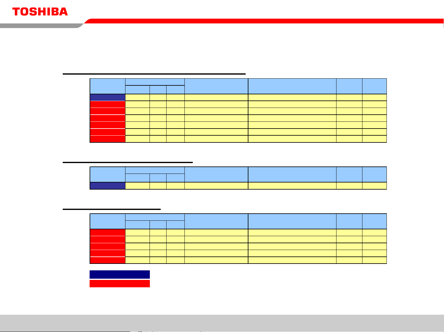
High Voltage TR for TV / Monitor
)
1. Progressive/ High Vision/Digital TV
2
Max. Rating
V
(V) IC(A) PC(W)
CBO
1700 8 55 24 to 32inc h / to 31.5 kHz
1700 15 70 24 to 36 inc h / to 45kHz
1700 21 75 28 to 36 inc h / to 45 kHz
1700 22 200 32 to 36 inc h / to 45 kHz
1700 23 200 32 to 36 inc h / to 45 kHz
2000 14 75 28 to 32 inc h / to 45 kHz
2000 16 210 28 to 36 inc h / to 45 kHz
NEW !
NEW !
NEW !
NEW !
Part Number Display size & Frequency MPSampleDevice Outline
2SC5716
2SC6041
2SC5857
2SC5858
2SC5859
2SC5997
2SC5748
2. Color TV (Conventional)
Part Number
2SD2638
Max. Rating
V
(V) IC(A) PC(W)
CBO
1700 7 50 24 to 32 inch / 15.75 k Hz New generation of 2SD2553 OK OK
3. PC Monitor (CRT)
Max. Rating
V
(V) IC(A) PC(W)
CBO
1500 21 75 19 inch / to 120 kHz TO-3P(H)IS version of 2SC5445 OK OK
1500 22 200 21inch / to 130 kHz New genetaiton of 2SC5445 OK OK
1700 23 210 19 inch / to 100 kHz
1500 10 50 17 inch / to 69 kHz New generation of 2SC5387 OK OK
1500 14 55 19 inch / to 92 kHz New generation of 2SC5411 OK OK
NEW !
NEW !
Part Number
2SC5717
2SC5695
2SC5859
2SC5855
2SC5856
with high speed dumper diode(31.5kHz)
New generationg of 2SC5588
New generationg of 2SC5588( High current
New generation of 2SC5590(High Current)
New generation of 2SC5446(High Current)
TO-3P(H)IS version of VCBO=2000V TR
High current version of VCBO=2000V TR
Display size & Frequency Device Outline Sample MP
Display size & Frequency Device Outline
New generation of 2SC5446(High Current)
OK OK
OK OK
OK OK
OK OK
OK OK
OK OK
OK OK
Sample MP
OK OK
2SC… & 2SD…
2SC…
: Fourth Generation
: Fifth generation
DP0540034_01Transistors
Page 3
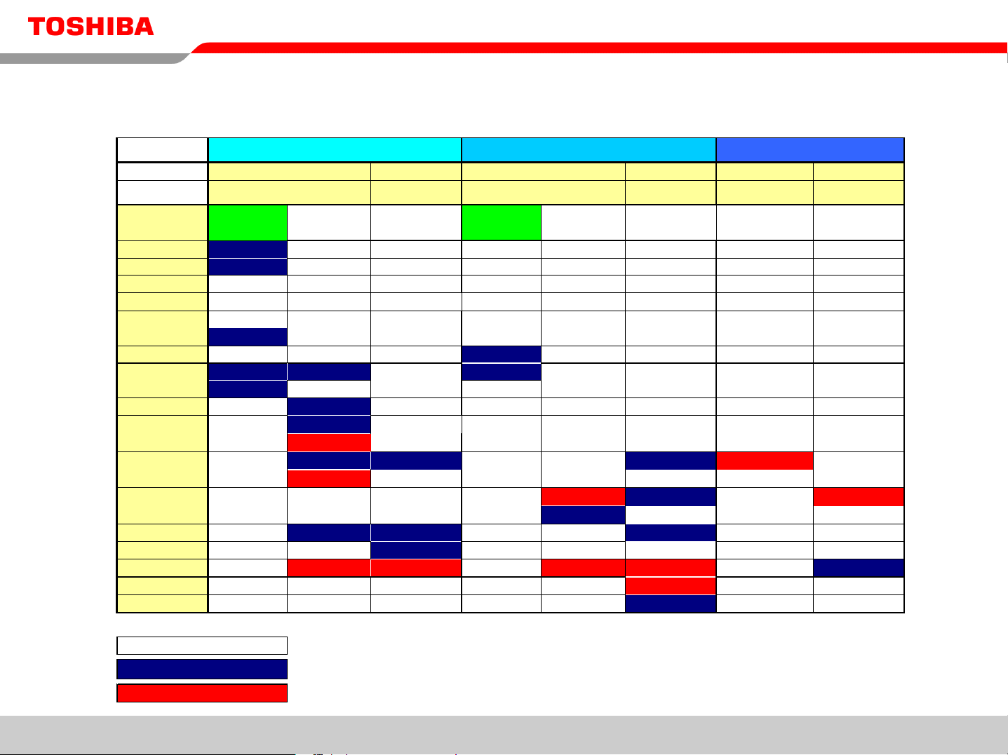
Line up (by Voltage & Current)
3
V
=1500V V
CBO
Package
P
max
C
*I
C(sat)
3 A 2SD2599 2SD2550
3.5 A 2SD2586
4 A 2SD2499 2SD2498 2SD2551
4.5 A S2055N S2000N
5 A 2SD2539
5.5 A 2SD2638
6 A 2SC5280 2SC5386 2SC5716
7 A 2SC5404
8 A 2SC5387
11 A 2SC5411 2SC5421 2SC5422 2SC5997
12 A 2SC6041 2SC5590 2SC5748
14 A 2SC5587 2SC5589 2SC5446
15 A 2SC5445
17 A 2SC5717 2SC5695 2SC5857 2SC5858 2SC5612
18 A 2SC5859
22 A 2SC5570
TO-3P(H)IS TO-3P(LH) TO-3P(H)IS TO-3P(LH) TO-3P(H)IS TO-3P(LH)
40-75W 180-220W 40-75W 180-220W 40-75W 180-220W
with without without with without without without without
Dumper Dumper Dumper Dumper Dumper Dumper Dumper Dumper
2SC5339
2SD2559 2SD2500 2SD2553
2SC5855
2SC5856
=1700V
CBO
2SC5588
V
CBO
=2000V
Note
2SD… & S2…
2SC… & 2SD…
2SC…
: Third generation
: Fourth generation * Ic(sat) = IC at Vce=Vce(sat)
: Fifth generation
DP0540034_01Transistors
Page 4

Line up (2SC series)
4
Part Number MP V
2SC5339
2SC5280
2SC5386
2SC5404
2SC5387
2SC5411
2SC5421
2SC5587
2SC5589
2SC5445
2SC5716
2SC5588
2SC5422
2SC5590
2SC5446
2SC5570
2SC5612
NEW ! 2SC5855
NEW ! 2SC5856
2SC5717
2SC5695
NEW ! 2SC6041
NEW ! 2SC5857
NEW ! 2SC5858
2SC5859
NEW ! 2SC5997
2SC5748
Note
2SC… & 2SD…
2SC…
CBOIC
(V) (A) (W) (-) (-) (A) (V) (A) (A) (us) (us) (kHz) (A)
OK
OK
OK
OK
OK
OK
OK
OK
OK
OK
OK
OK
OK
OK
OK
OK
OK
OK
OK
OK
OK
OK
OK
OK
OK
OK
OK
1500 7 50
1500 8 50
1500 8 50
1500 9 50
1500 10 50
1500 14 60
1500 15 180
1500 17 75
1500 18 200
1500 20 200
1700 8 55
1700 15 75
1700 15 200
1700 16 200
1700 18 200
1700 28 220
2000 22 220
1500 10 50
1500 14 55
1500 21 75
1500 22 200
1700 15 70
1700 21 75
1700 22 200
1700 23 210
2000 14 75
2000 16 210
: Fourth generation
: Fi fth gena rtiong
Max. Rating
Dumper
P
Diode Min. Max. @5V/I
C
○
○
x
x
x
x
x
x
x
x
○
x
x
x
x
x
x
x
x
x
x
x
x
x
x
x
x
4.0 8.0 5 5 5 1.25 4.0 0.20 32 5.0
4.0 8.5 6 5 6 1.5 4.0 0.20 32 6.0
4.3 7.5 6 3 6 1.5 2.5 0.15 64 5.0
4.0 8.0 7 3 7 1.75 2.5 0.15 64 5.5
4.3 7.8 8 3 8 2 2.5 0.15 64 6.0
4.0 8.0 11 3 11 2.75 2.5 0.15 64 8.5
4.0 8.0 11 3 11 2.75 2.5 0.15 64 8.5
5.0 8.0 14 3 14 3.5 1.8 0.10 100 7.5
5.0 8.0 14 3 14 3.5 1.8 0.10 100 7.5
4.5 8.5 15 3 15 3.75 2.0 0.10 100 8.0
3.8 9.0 6 5 6 1.5 3.5 0.20 32 5.5
4.8 8.0 12 3 12 3 1.8 0.10 100 6.5
4.5 8.5 11 3 11 2.75 2.5 0.15 64 8.0
4.8 8.0 12 3 12 3 1.8 0.10 100 6.5
4.0 8.0 14 3 14 3.5 2.1 0.10 100 7.0
4.5 7.5 22 3 22 5.5 1.4 0.10 130 8.0
4.8 9.0 17 3 17 4.25 4.0 0.15 32 8.0
4.3 6.7 8 3 8 2 2.3 0.10 80 5.5
4.5 7.8 11 3 11 2.75 1.8 0.10 100 6.5
4.5 8.5 17 3 17 3.75 1.6 0.10 100 8.0
4.5 8.5 17 3 17 3.75 1.6 0.10 100 8.0
5.0 7.5 12 1.5 12 3 3.5 0.10 45 7.0
5.0 7.5 17 1.5 17 4.25 3.5 0.10 45 8.0
5.0 7.5 17 1.5 17 4.25 3.5 0.10 45 8.0
4.5 8.0 18 3 18 4.5 1.8 0.10 100 7.5
5.0 7.2 11 1.5 11 2.75 5.0 0.12 32 6.0
4.8 7.5 12 3 12 3 4.0 0.15 32 8.0
h
FE
V
C
Max.
CE(sat)
@ IC@ I
Switching time (Typ.)
t
B
stg
t
f
@ fH@ I
CP
DP0540034_01Transistors
Page 5

Line up (2SD / S series)
(V)
(A)
(W)
(-)
(-)
(A)
(V)
(A)
(A)
(us)
(us)
(kHz)
(A)
5
Max. Rating
Part Number
2SD2498 OK 1500 6 50 5 9 4 5 4 0.8 10 0.7 15.75 4
2SD2499 OK 1500 6 50
2SD2539 OK 1500 7 50
2SD2500 OK 1500 10 50 4 8 6 3 6 1.5 11 0.7 15.75 6
2SD2550 OK 1700 4 50
2SD2551 OK 1700 5 50
2SD2553 OK 1700 8 50
2SD2599 OK 1500 3.5 40
2SD2586 OK 1500 5 50
2SD2559 OK 1500 8 50
2SD2638 OK 1700 7 50
S2000N OK 1500 8 50 4.5 9 4.5 5 4.5 1 12 0.7 15.75 4.5
S2055N OK 1500 8 50
2SD… & S2…
2SD…
MP V
CBOIC
: Third generation
: Fourth generation
PCDumper Min. Max. @5V/I
with
○
○
○
○
○
○
○
○
○
○
4.4 8.5 3.5 5 3.5 0.8 10 0.6 15.75 3.5
4.5 7.5 5.5 5 5.5 1.2 9 0.8 15.75 5.5
4.5 9 4.5 5 4.5 1 11 0.6 15.75 4.5
h
FE
C
5 9 4 5 4 0.8 11 0.6 15.75 4
5 9 5 5 5 1 9 0.6 15.75 5
8 22 1 8 3 0.8 10 0.6 15.75 3
5 10 4 5 4 0.8 10 1.0 15.75 4
5 9 6 5 6 1.2 12 0.7 15.75 6
8 25 0.5 8 3 0.8 10 1.0 15.75 3
5 9 6 5 6 1.2 12 1.0 15.75 6
V
Max.
CE(sat)
@ IC@ I
Switching time
t
B
stg
t
@ f
f
@ I
H
CP
DP0540034_01Transistors
Page 6

r
)
(
)
TR selection guide( for TV)
For reference
V
=1500V
CBO
Display size
Flat TV / Wide TV / Projecto
: D1terminal ( 525i / fH=15.75kHz
9 to 16 inch
16 to 20 inch
20 to 24 inch
24 to 28 inch
28 to 32 inch
32 to 36 inch
more than 36 inch
Progressive, High Vision / TV , Projector
: D2 terminal ( 525p / fH= 31.5kHz ), D3 terminal ( 1125i / fH=33.75kHz )
24 to 28 inch
28 to 32 inch
32 to 36 inch
more than 36 inch
with dumper diode without dumper diode with dumper diode without dumper diode
2SD2599 2SD2550
2SD2586 2SD2550
2SD2499 or S2055N 2SD2498 or S2000N 2SD2551
2SD2539 or 2SC5339 2SD2500 2SD2638 or 2SD2553
2SD2559 or 2SC5280 2SC5386 or 2SC5404 2SD2553 or 2SC5716 or 2SD2638 2SC5997
2SC5855 2SC6041 2SC5997
2SC5856 2SC6041
2SC5855 2SC5716 2SC6041 2SC5997
2SC5856 or 2SC5587 2SC5716 2SC6041 2SC5997
2SC5856 or 2SC5587 2SC5857 or 2SC6041 2SC5748
2SC5589 or 2SC5717
or 2SC5695
V
CBO
=1700V
2SC5858 or 2SC5859 2SC5748 or 2SC5612
V
=2000V
CBO
without dumper diode
6
High vision / Digital TV
: D3 terminal
28 to 32 inch
32 to 36 inch
more than 36 inch
NOTE 1 ; How to calculate displaysize ; Siz e (inch)=Icp×(4.5 to 5.5 ) @D1 terminal
1125i / fH=33.75kHz , D4 terminal ( 750p / fH = 45kHz
2SC5280(HFE)×2 series
2SC6041×2s eries2SC5856×2 s eries
2SC5587×2 s eries
2SC5717×2s eries
Size (inch)=Icp×(3.5 to 4.0 ) @D2, D3 terminal
2SC5857×2s eries or
2SC6041×2s eries
2SC5858×2s eries or
2SC5857×2 s ereis
2SC5748 or 2SC5997
2SC5748 or 2SC5612
2SC5612
DP0540034_01Transistors
Page 7

Switching wave form & Chip pattern & : 3 G to 5G
7
Third Generation
Priority design for
high breakdown level
Standard for TV use
Fourth Generation
Improved switching & Vce(sat)
by mesh pattern
Low power loss by Vce(sat) from
5v to 3V (Max.)
Fifth Generation
Comb pattern
Mesh pattern
Super mesh pattern
High voltage(1700V, 200V) & high
current available , keeping 4
characteristics
Vce(sat)=1.5V TR developed for TV
and lower power loss type possible
th
G.
DP0540034_01Transistors
Page 8

The information contained herein is subject to change without notice. 021023_D
The information contained herein is presented only as a guide for the applications of our products. No responsibility is assumedby
TOSHIBA for any infringements of patents or other rights of the third parties which may result from its use. No license is granted by
implication or otherwise under any patent or patent rights of TOSHIBA or others. 021023_C
TOSHIBA is continually working to improve the quality and reliability of its products. Nevertheless, semiconductor devices in
general can malfunction or fail due to their inherent electrical sensitivity and vulnerability to physical stress.
It is the responsibility of the buyer, when utilizing TOSHIBA products, to comply with the standards of safety in making a safe
design for the entire system, and to avoid situations in which a malfunction or failure of such TOSHIBA products could cause loss
of human life, bodily injury or damage to property.
In developing your designs, please ensure that TOSHIBA products are used within specified operating ranges as set forth in the
most recent TOSHIBA products specifications.
Also, please keep in mind the precautions and conditions set forth in the “Handling Guide for Semiconductor Devices,” or
“TOSHIBA Semiconductor Reliability Handbook” etc. 021023_A
The Toshiba products listed in this document are intended for usage in general electronics applications (computer, personal equipment,
office equipment, measuring equipment, industrial robotics, domestic appliances, etc.).
These Toshiba products are neither intended nor warranted for usage in equipment that requires extraordinarily high quality and/or
reliability or a malfunction or failure of which may cause loss of human life or bodily injury (“Unintended Usage”). Unintended Usage
include atomic energy control instruments, airplane or spaceship instruments, transportation instruments, traffic signal instruments,
combustion control instruments, medical instruments, all types of safety devices, etc. Unintended Usage of Toshiba products listed in this
document shall be made at the customer’s own risk. 021023_B
8
The products described in this document may include products subject to the foreign exchange and foreign trade laws. 021023_F
The products described in this document may contain components made in the United States and subject to export control of the U.S.
authorities. Diversion contrary to the U.S. law is prohibited. 021023_H
TOSHIBA products should not be embedded to the downstream products which are prohibited to be produced and sold, under any law and
regulations. 030519_Q
DP0540034_01Transistors
 Loading...