

Toshiba 65L9400U Series Service Manual

SERVICE MANUAL
LCD Color Television
65L9400U series
(System Information)
FILE NO. 050-2014124

CONTENTS
1. IMPORTANT NOTICE
2. GREEN PRODUCT PROCUREMENT
3. LEAD-FREE SOLDER
4. SAFETY INSTRUCTION
5. SERVICE MODE
6. LED INDICATIONS FOR SERVICE
7. FIRMWARE UPDATING
8. MAIN BOARD EXCHANGE
9. SETTING SHIPOUT CODE (when Main board is
exchanged)
10. INTERCONNECT
11. SCHEMATIC DIAGRAM
1

IMPORTANT NOTICE
WARNING:
You are requested that you shall not modify or alter the information or data provided
herein without prior written consent by Toshiba. Toshiba shall not be liable to
anybody for any damages, losses, expenses or costs, if any, incurred in connection
with or as a result of such modification or alteration.
THE INFORMATION OR DATA HEREIN SHALL BE PROVIDED "AS IS" WITHOUT ANY
WARRANTY OF ANY KIND, EITHER EXPRESS OR IMPLIED WARRANTY OF
MERCHANTABILITY AND FITNESS FOR A PARTICULAR PURPOSE.
Toshiba shall not be liable for any damages, losses, expenses or costs, if any,
incurred in connection with or as a result of use of any information or data provided
herein.

GREEN PRODUCT P ROCUREMENT
The EC is actively promoting the WEEE & RoHS Directives that define standards for
recycling and reuse of Waste Electrical and Electronic Equipment and for the Restriction of
the use of certain Hazardous Substances. From July 1, 2006, the RoHS Directive will
prohibit any marketing of new products containing the restricted substances.
Increasing attention is given to issues related to the global environmental. Toshiba
Corporation recognizes environmental protection as a key management tasks, and is doing
its utmost to enhance and improve the quality and scope of its environmental activities. In
line with this, Toshiba proactively promotes Green Procurement, and seeks to purchase
and use products, parts and materials that have low environmental impacts.
Green procurement of parts is not only confined to manufacture. The same green parts
used in manufacture must also be used as replacement parts.
LEAD-FREE SOLDER
This product is manufactured using lead-free solder as a part of a movement within the
consumer products industry at large to be environmentally responsible. Lead-free solder
must be used in the servicing and repair of this product.
WARNING: This product is manufactured using lead free solder.
DO NOT USE LEAD BASED SOLDER TO REPAIR THIS PRODUCT!
The melting temperature of lead-free solder is higher than that of leaded solder by 54ºF to
72ºF (30ºC to 40ºC). Use of a soldering iron designed for lead-based solders to repair
product made with lead-free solder may result in damage to the component and or PCB
being soldered. Great care should be made to ensure high-quality soldering when servicing
this product especially when soldering large components, through-hole pins, and on PCBs
as the level of heat required to melt lead-free solder is high.

(1/3)
SAFETY INSTRUCTION
WARNING: BEFORE SERVICING THIS CHASSIS, READ THE "SAFETY
PRECAUTION" AND "PRODUCT SAFETY NOTICE" INSTRUCTIONS BELOW.
Safety Precaution
WARNING: SERVICING SHOULD NOT BE ATTEMPTED BY ANYONE UNFAMILIAR
WITH THE NECESSARY PRECAUTIONS ON THIS RECEIVER. THE FOLLOWING ARE
THE NECESSARY PRECAUTIONS TO BE OBSERVED BEFORE SERVICING THIS
CHASSIS.
1. An isolation transformer should be connected in the power line between the receiver
and the AC line before any service is performed on the receiver.
2. Always disconnect the power plug before any disassembling of the product. It may
result in electrical shock.
3. When replacing a chassis in the cabinet, always be certain that all the protective
devices are put back in place, such as nonmetallic control knobs, insulating covers,
shields, isolation resistor-capacitor network, etc.
4. Always keep tools, components of the product, etc away from the children, These
items may cause injury to children.
5. Depending on the model, use an isolation transformer or wear suitable gloves when
servicing with the power on, and disconnect the power plug to avoid electrical shock
when replacing parts. In some cases, alternating current is also impressed in the
chassis, so electrical shock is possible if the chassis is contacted with the power on.
6. Always use the replacement parts specified for the particular model when making
repairs. The parts used in products require special safety characteristics such as
inflammability, voltage resistance, etc. therefore, use only replacement parts that
have these same characteristics. Use only the specified parts when the
mark is
indicated in the circuit diagram or parts list.
7. Parts mounting and routing dressing of wirings should be the same as that used
originally. For safety purposes, insulating materials such as isolation tube or tape are
sometimes used and printed circuit boards are sometimes mounted floating. Also
make sure that wirings is routed and clamped to avoid parts that generate heat and
(2/3)
which use high voltage. Always follow the manufactured wiring routes / dressings.
8. Always ensure that all internal wirings are in accordance before re-assembling the
external casing after a repairing completed. Do not allow internal wiring to be
pinched by cabinets, panels, etc. Any error in reassembly or wiring can result in
electrical leakage, flame, etc., and may be hazardous.
9. NEVER remodel the product in any way. Remodeling can result in improper
operation, malfunction, or electrical leakage and flame, which may be hazardous.
10. Always perform an AC leakage current checking on the exposed metallic parts of the
cabinet such as antennas, terminals, screw heads, metal overlays, control shafts
and etc. to be sure that the set is safe to operate without any dangerous of electrical
shocks before returning the set to the customer.
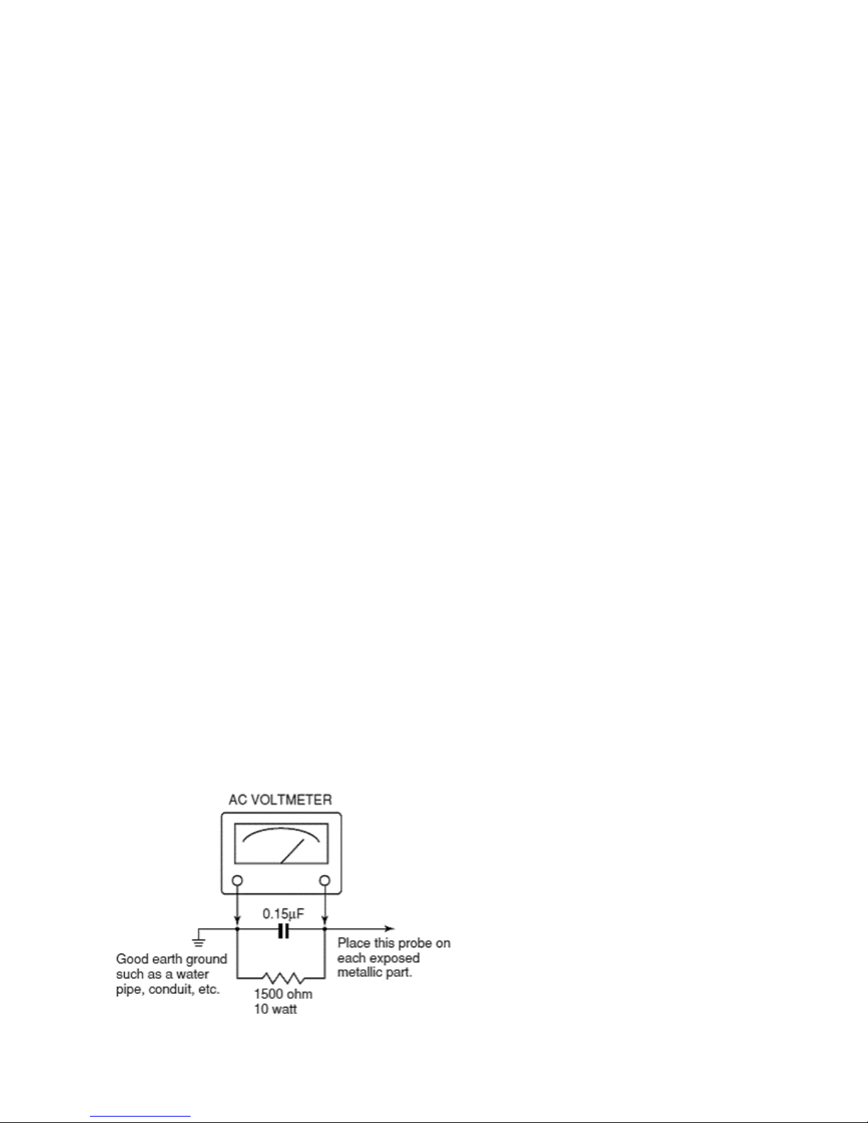
11. The leakage current checking. (After completing the work, measure the leakage
current to prevent an electrical shock.)
Plug the AC line cord directly into a 120V AC outlet. Do not use an isolation
transformer for this check.
Use an AC voltmeter having 5000 ohms per volt or more sensitivity in the following
manner.
Connect a 1500 ohm 10 watt resistor, paralleled by a 0.15 µF, AC type capacitor, between
a known good earth ground (water pipe, conduit, etc.) and the exposed metallic parts, one
at a time. Measure the AC voltage across the combination of 1500 ohm resistor and 0.15
µF capacitor. Reverse the AC plug at the AC outlet and repeat AC voltage measurements
for each exposed metallic part. Voltage measured must not exceed 0.3 volts rms. This
corresponds to 0.2 milliamp. AC. Any value exceeding this limit constitutes a potential
shock hazard and must be corrected immediately.

(3/3)
Product Safety Notice
Many electrical and mechanical parts in this chassis have special safety-related
characteristics. These characteristics are often passed unnoticed by a visual inspection and
the protection afforded by them cannot necessarily be obtained by using replacement
components rated for higher voltage, wattage, etc. Replacement parts which have these
special safety characteristics are identified in this manual and its supplements; electrical
components having such features are identified by the international hazard symbols on the
schematic diagram and the parts list.
Before replacing any of these components, read the parts list in this manual carefully. The
use of substitute replacement parts which do not have the same safety characteristics as
specified in the parts list may create electrical shock, fire, or other hazards.

(1/3)
SERVICE MODE
ENTERING SERVICE MODE
1. Press MUTE button twice on Remote Control.
TV mode changes as follows. Un-Mute => 1/2Mute => Mute
2. Press MUTE button again and keep pressing.
(Sound Mute is canceled)
3. While pressing the MUTE button, press CH/INPUT button on TV control panel.
(Enter Service Mode)
(2/3)
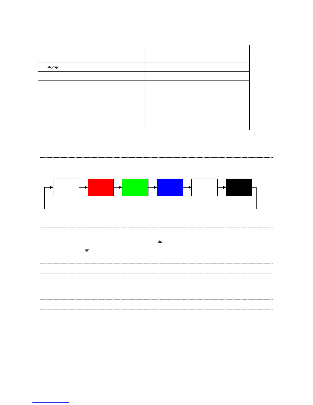
KEY FUNCTION IN THE SERVICE MODE
The following key entry during display of adjustment menu provides special functions.
Button Function
INPUT button (on Remote) Test signal selection
CH (on Remote) Selection of the adjustment items
VOL +/– (on Remote) Change of the data value
[7] button Automatic A/D Adjustment
(PC, Component, Composite(PAL, NTSC))
[9] button Self Check display ON
[Exit] button Exit from Service mode
Self Check display Off
CAUTION: Never try to perform initialization unless you have changed the memory IC.
TEST SIGNAL SELECTION
1) While displaying the adjustment menu, every pressing of INPUT button on the Remote Control changes the
built-in test patterns on screen as described below.
When a pattern is changed at the time of an ATV display, it can display only for a moment.
SELECTING THE ADJUSTING ITEMS
1) While displaying the adjustment menu, press the CH button to cycle through the adjustment items in the
order of table. (CH
button for reverse order)
ADJUSTING THE DATA
1) While displaying the adjustment menu, press the VOL +/– button to change the value of data in the range
from 00H to FFH. The variable range depends on the adjusting item.
EXIT FROM SERVICE MODE
1) Press the [Exit] button on Remote.
Normal
Picture
Red screen Green screen
Blue screen

(3/3)
ADJUSTING ITEMS IN THE SERVICE MODE
Item Description
RCUT RED CUTOFF
GCUT GREEN CUTOFF
BCUT BLUE CUTOFF
RDRV RED DRIVE
GDRV GREEN DRIVE
BDRV BLUE DRIVE
OSRC COOL R-CUTOFF-OFFSET for COOL
OSRC NATURAL R-CUTOFF-OFFSET for NATURAL
OSRC WARM R-CUTOFF-OFFSET for WARM
OSGC COOL G-CUTOFF-OFFSET for COOL
OSGC NATURAL G-CUTOFF-OFFSET for NATURAL
OSGC WARM G-CUTOFF-OFFSET for WARM
OSBC COOL B-CUTOFF-OFFSET for COOL
OSBC NATURAL B-CUTOFF-OFFSET for NATURAL
OSBC WARM B-CUTOFF-OFFSET for WARM
OSRD COOL R-DRIVE-OFFSET for COOL
OSRD NATURAL R-DRIVE-OFFSET for NATURAL
OSRD WARM R-DRIVE-OFFSET for WARM
OSGD COOL G-DRIVE-OFFSET for COOL
OSGD NATURAL G-DRIVE-OFFSET for NATURAL
OSGD WARM G-DRIVE-OFFSET for WARM
OSBD COOL B-DRIVE-OFFSET for COOL
OSBD NATURAL B-DRIVE-OFFSET for NATURAL
OSBD WARM B-DRIVE-OFFSET for WARM
OSRD 3D COOL R-DRIVE-OFFSET for COOL (3D)
OSRD 3D NATURAL R-DRIVE-OFFSET for NATURAL (3D)
OSRD 3D WARM R-DRIVE-OFFSET for WARM (3D)
OSGD 3D COOL G-DRIVE-OFFSET for COOL (3D)
OSGD 3D NATURAL G-DRIVE-OFFSET for NATURAL (3D)
OSGD 3D WARM G-DRIVE-OFFSET for WARM (3D)
OSBD 3D COOL B-DRIVE-OFFSET for COOL (3D)
OSBD 3D NATURAL B-DRIVE-OFFSET for NATURAL (3D)
OSBD 3D WARM B-DRIVE-OFFSET for WARM (3D)
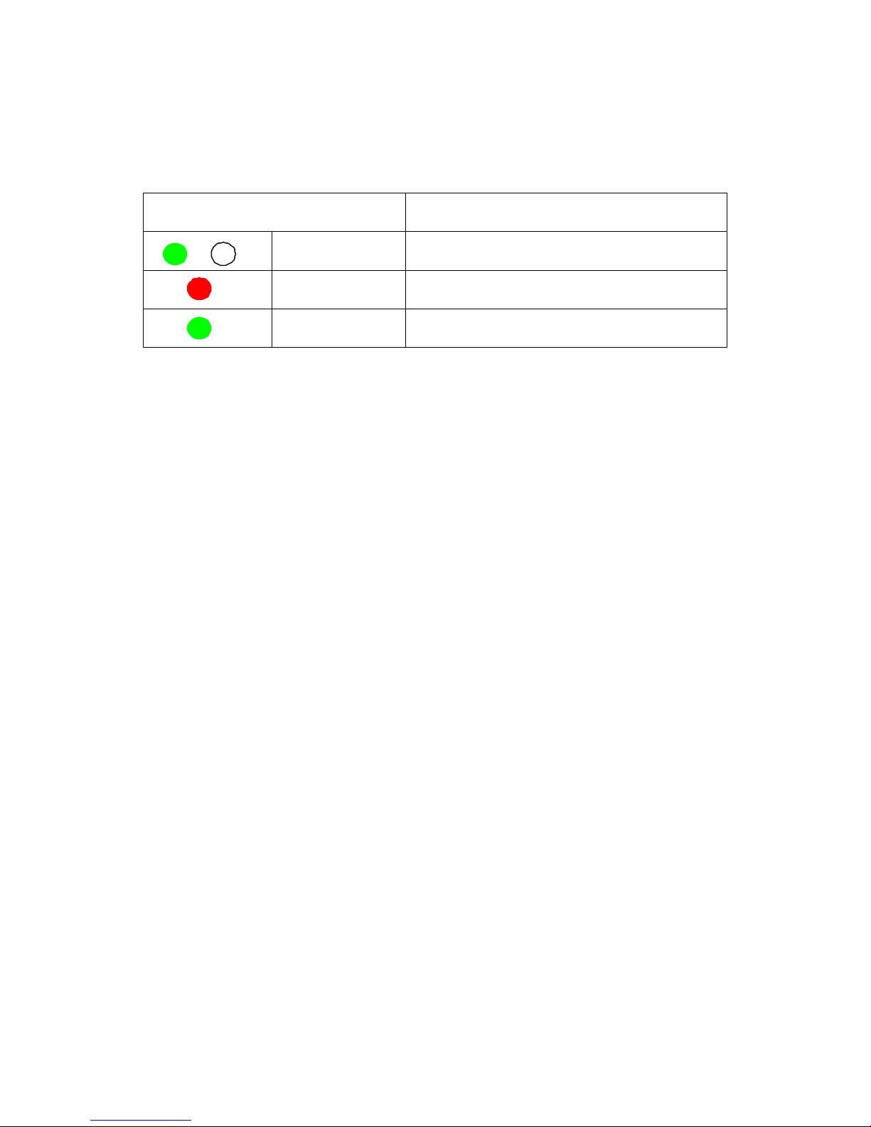
LED INDICATIONS FOR SERVICE
SW Upgrade and Error conditions indicated by the Power LED is described below.
Power LED
Green blink SW Upgrade in Progress
Red SW Upgrade Failed
Green SW Upgrade Successful
/

(1/3)
FIRMWARE UPDATING
To upgrade FW for L8400U/L9400U series via USB mass storage device, please follow the
steps below:
1. Use the USB mass storage device formatted with “FAT32”.
2. Copy the following 3 files to the root directory of the USB mass storage device.
Model: 58L8400U
L8400.meta
L8400_FRC_xxxx.fwu
L9400_9.12.xx.yy.zz.1.fwu
("9.12.xx.yy.zz.1" is a FW version number.) (Same as L9400 model)
Model: 65L9400U
L9400.meta
L9400_FRC_xxxx.fwu
L9400_9.12.xx.yy.zz.1.fwu
("9.12.xx.yy.zz.1" is a FW version number.)
3. Plug and turn on the DTV, waiting until the picture is displayed on the screen.
4. Insert the USB mass storage device to the USB-1 slot(Bottom side) of the DTV.

(2/3)
6. Then, the following message appears to enable users to select their preferable behaviour
after the SW upgrade completes. If YOU want DTV to reboot automatically after FW
upgrade, select “Yes”. If YOU want DTV to go to standby after that, select “No”.
5. After the following message appears, select “Yes” with Left/Right key, and push “OK”
key to start FW upgrade.

9. If FW upgrade succeeds, the following message appears. After that, the DTV will reboot
or go to standby automatically according to the user setting on No.6 above.
10. Unplug USB mass storage device from the DTV.
8. After that, the following gauge screen appears. Wait until the gauge display reaches
100%.
7. When FW upgrade starts, the following message appears. Please leave the DTV alone
until FW upgrade completes as described in No.9 below.
MAIN BOARD EXCHANGE
1. Whenever Main Board is exchanged, you are required to confirm the Destination (Ship
Out Code Setting).
If the Setting is not valid, change the Ship Out Code.
(See “SETTING SHIPOUT CODE_TM14NA4K”)
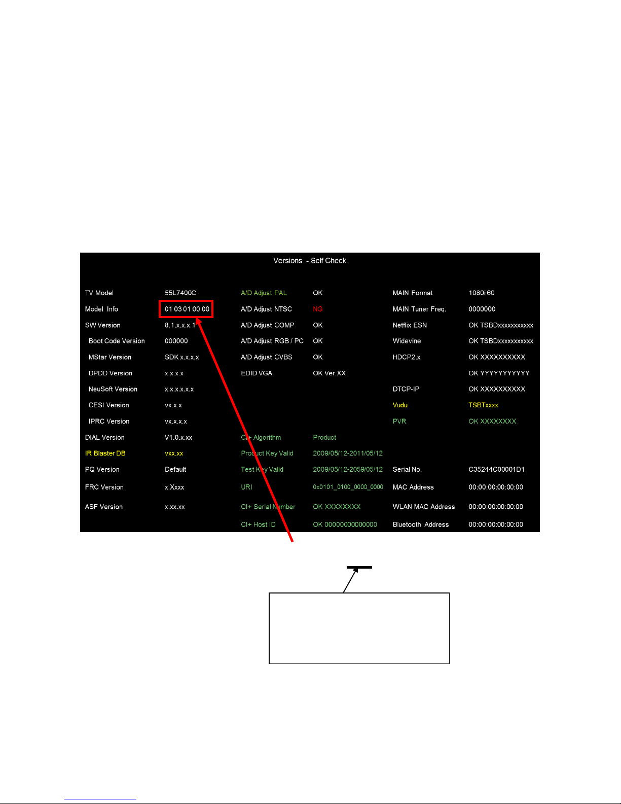
2. Check the shipout code by using self check screen.
How to enter the self check screen.
1 Press SETUP on remote control unit.
2 Select “Get Help” >> “System Information”
3 Press “3” “5” “7” “4”
00 00 00 00 00
The 4th byte is the Shipout code.
00: USA
01: Canda
02: Mexico

(1/3)
SETTING SHIPOUT CODE (when Main board
is exchanged)
When Main board is exchanged, the shipout code needs to be set up according to the each
Destination.
Please install the each Model Setting File in the following procedure.
1. Use the USB mass storage device formatted with “FAT32”.
2. Copy the following file to the root of the USB mass storage device.
<Use below file to change the shipout code to USA>
58L8400U: USA¥Model_Setting_L8400_58_C.bin
65L9400U: USA¥Model_Setting_L9400_65_C.bin
<Use below file to change the shipout code to Canada>
58L8400UC: Canada¥Model_Setting_L8400_58_C.bin
65L9400UC: Canada¥Model_Setting_L9400_65_C.bin
<Use below file to change the shipout code to Mexico>
58L8400UM: Mexico¥Model_Setting_L8400_58_C.bin
65L9400UM: Mexico¥Model_Setting_L9400_65_C.bin

(2/3)
3. Insert the USB mass storage device USB-1 slot(Bottom side) of the TV set.
4. While pushing “VOL –“ key on the local key that is installed on the si de of DTV, plug and
turn on the DTV, waiting for TOSHIBA logo OSD to appear.
5. Wait for about 2 minutes, and unplug USB mass storage device.
6. Push “MENU” key on the remote, select “Installation”> > “Reset TV”.
7. After the following message appears, select “Yes” with Left/Right key, and
push“OK”key.
8. Following the success of “Reset TV”, shipout change becomes valid.

(3/3)
9. Check the shipout code by using self check screen.
How to enter the self check screen.
1 Push “MENU” key on the remote.
2 Select “Get Help” >> “System Information”
3 Press “3” “5” “7” “4”
00 00 00 00 00
The 4th byte is the Shipout code.
00: USA
01: Canda
02: Mexico

CN30 CN90 CN650 CN651 CN652
CN201 CN202 CN102 PJ91 PJ90 1 R+_AMP 1 12V 1 CML_GND 1 NC 1 TE ST-MODE
1 L64_Cathode 1 R11_Anode 1 GND 1 AC_DETECT 1 12V 2 R-_AMP 2 12V 2 VX1TX7P 2 Temp_SEL0 2 VSYNC_IN
2 L34_Cathode 2 R41_Anode 2 NC 2 POWER_TV 2 12V 3 L-_AMP 3 12V 3 VX1TX7N 3 Temp_SEL1 3 GND
3 L63_Cathode 3 R12_Anode 3 TEST-MODE 3 5V1 3 12V 4 L+_AMP 4 12V 4 CML_GND 4 NC 4 SCREEN_SIZE
4 L33_Cathode 4 R42_Anode 4 NC 4 GND 4 12V 5 GND 5 VX1TX6P 5 NC 5 BL_ONOFF
5 L62_Cathode 5 R13_Anode 5 VSYNC-IN 5 18V(LNB) 5 GND 6 GND 6 VX1TX6N 6 NC 6 SERIAL_DATA
6 L32_Cathode 6 R43_Anode 6 NC 6 GND 6 GND CN45 7 GND 7 CML_GND 7 NC 7
SERIAL_CLK
7 L61_Cathode 7 R14_Anode 7 GND 7 BL_ON/OFF 7 GND 1 3.3V_TVM 8 GND 8 VX1TX5P 8 NC 8 GND
8 L31_Cathode 8 R44_Anode 8 SCREEN SIZE 8 POWER_LCD 8 GND 2 REMOTE_IN 9 18.5V_AUDIO 9 VX1TX5N 9 NC 9 3D_EN
9 L54_Cathode 9 R21_Anode 9 BL_ONOFF 9 NC 3 GND 10 18.5V_AUDIO 10 CML_GND 10 NC
10 L24_Cathode 10 R51_Anode 10 SERIAL_DATA 4 OP_IN 11 GND_AUDIO 11 VX1TX4P 11 NC
11 L53_Cathode 11 R22_Anode 11 GND 5 3.3VD 12 GND_AUDIO 12 VX1TX4N 12 NC
CN165
12 L23_Cathode 12 R52_Anode 12 SERIAL_CLK PJ92 6 5V1 13 CML_GND 13 NC 1 5V_WLAN
13 L52_Cathode 13 R23_Anode 13 GND 1 18V(Audio) 7 GND 14 VX1TX3P 14 NC 2 S_USBO2DM
14 L22_Cathode 14 R53_Anode 14 3 D_EN 2 18V(Audio) 8 LED_GREEN 15 VX1TX3N 15 NC 3 S_USBO2DP
15
L51_Cathode 15 R24_Anode 15 GND 3 GND(Audio ) 9 LE D_RED 16 CML_GND 16 NC 4 GND
16 L21_Cathode 16 R54_Anode 4 GND(Audio) 10 KEY_POWER 17 VX1TX2P 17 CML_GND 5
C_WWOL_WAKEUP
17 L44_Cathode 17 R31_Anode 11 KEY_IN2 CN91 18 VX1TX2N 18 VX1TX15P 6 GND
18 L14_Cathode 18 R61_Anode 12 GND 1 AC_DETECT 19 CML_GND 19 VX1TX15N
19 L43_Cathode 19 R32_Anode 13 KEY_IN1 2 POWER_TV 20 VX1TX1P 20 CML_GND
20 L13_Cathode 20 R62_Anode PJ93 3 5V 21 VX1TX1N 21 VX1TX14P
21 L42_Cathode 21 R33_Anode CN101 PJ860 1 GND 4 GND 22 CML_GND 22 VX1TX14N
22 L12_Cathode 22 R63_Anode 1 GND 1 GND(LE D) 2 GND 5 18V_LNB 23 VX1TX0P 23 CML_GND
23 L41_Cathode 23 R34_Anode 2 GND 2 GND(LE D) 3 12V CN355 6 GND 24 VX1TX0N 24 VX1TX13P
24 L11_Cathode 24 R64_Anode 3 GND 3 GND(LE D) 4 12V
1 7 BL-ONOFF 25 CML_GND 25 VX1TX13N
25 NC 25 NC 4 GND 4 GND(LED) 5 12V 2 8 POWER_LCD 26 LOCKN 26 CML_GND
26 NC 26 NC 5 GND 5 GND(LED) 6 NC 3 9 POWER-DB 27 HTPDN 27 VX1TX12P
27 L64_Anode 27 R11_Cathode 6 GND 6 GND(LED) 4 10 PWM 28 GND 28 VX1TX12N
28 L34_Anode 28 R41_Cathode 7 GND 7 GND(LED) 5 29 3D_S YNCI 29 CML_GND
29 L63_Anode 29 R12_Cathode 8 18V(LED)/24V(LED) 8 18V(LED)/24V(LED) 6 30 3D_S YNCO 30 VX1TX11P
30 L33_Anode 30 R42_Cathode 9 18V(LED)/24V(LED) 9 18V(LED)/24V(LED) 7 31 3D_E N 31 VX1TX11N
31 L62_Anode 31 R13_Cathode 10 18V(LED)/24V(LED) 10 18V(LED)/24V(LED) 8 32 NC 32 CML_GND
32 L32_Anode 32 R43_Cathode 11 18V(LED)/24V(LED) 11 18V(LED)/24V(LED) 9 33 NC 33 VX1TX10P
33 L61_Anode 33 R14_Cathode 12 18V(LED)/24V(LED) 12 18V(LED)/24V(LED) 10 34 NC 34 VX1TX10N
34 L31_Anode 34 R44_Cathode 13 18V(LED)/24V(LED) 13 18V(LED)/24V(LED) 11 35 NC 35 CML_GND
35 L54_Anode 35 R21_Cathode 14 18V(LED)/24V(LED) 14 18V(LED)/24V(LED) 12 36 NC 36 VX1TX9P
36 L24_Anode 36 R51_Cathode 13 3.3V_IO 37 NC 37 VX1TX9N
37 L53_Anode 37 R22_Cathode 14 GND 38 GND 38 CML_GND
38 L23_Anode 38 R52_Cathode 39 GND 39 VX1TX8P
39 L52_Anode 39 R23_Cathode 40 GND 40 VX1TX8N
40 L22_Anode 40 R53_Cathode 41 GND 41 CML_GND
41 L51_Anode 41 R24_Cathode 42 GND
42 L21_Anode 42 R54_Cathode 43 NC
43 L44_Anode 43 R31_Cathode 44 12V
44 L14_Anode 44 R61_Cathode 45 12V
45 L43_Anode 45 R32_Cathode 46 12V
46 L13_Anode 46 R62_Cathode 47 12V
47 L42_Anode 47 R33_Cathode CN46 48 12V
48 L12_Anode 48 R63_Cathode P801A 1 VCC_FAN 49 12V
49 L41_Anode 49 R34_Cathode 1 Line 2 GND 50 12V
50 L11_Anode
50 R64_Cathode 2 Neutral 3 STOP_FAN 51 12V
CN740
1 3.3V_TVM
2 RMT_IN
3 GND
4 OP_IN
5 3.3VD
CN401 6 5V1
1
C_POWER_KEY
7 GND
2
C_KEY2(MODE)
8 LED_GREEN
3
GND
9 LED_RED
4
C_KEY1(UP)(DOWN)
Speaker
PE1188
Main
LCON
65":
TYL5865TD048A01
T-CON
Speaker
AC IN
PANEL BACKLIGHT
PE1183
LED/REMOTE/SENSOR
POWER
65":
N13-535P1A
Cooling fan
WLAN
PE1121
KEY
MN860
MN93
MN30
MN45
MN90
MN91
MN46
MN6
MN165
MZ01
MZ02
U800
U811
U01A
U802
U03A
U04A
P801

TOSHIBA CORPORATION
APPROVED BY CHECKED BY TITLE TOTAL PAGE NO. REV.MARK DRAWING.NO.DESIGNED BY
5T03655-2E
12
13
14
15
17
18
19
20
FUNCTION
21
22
23
24
25
PAGE
16
10
1
2
3
4
5
6
7
8
9
11
PAGE
REV
FUNCTION
REV
PAGE FUNCTION FUNCTION
REV
PAGE
REV
44
45
46
47
48
49
27
28
50
29
30
31
32
33
34
35
36
37
38
26
39
40
41
42
43
55
54
64
53
70
52
65
51
75
71
62
74
66
68
58
63
57
73
59
69
72
61
67
56
60
95
94
93
92
91
90
89
88
87
86
85
84
83
82
81
80
79
100
78
77
76
99
98
97
96
PWA NAME
PWB NAME
UNIT NAME
PWB NO.
UNIT NO.
PWA NO.
SCHEMATIC DIAGRAMS
PRODUCT NAME
2014.08.06 16:14
CIRCUIT DIAGRAM 1 0
L84xx/L94xx MP
TITLE
MAIN UNIT
PE1188ZA
101 MSD8832WDK TS/USB/LAN 00
102 MSD8832WDK FLASH 00
103 MSD8832WDK DDR A 00
104 MSD8832WDK DDR B 00
105 MSD8832WDK GPIO 00
106 MSD8832WDK HDMI 00
107 MSD8832WDK LVDS/Vby1 00
108 MSD8832WDK AUDIO 00
109 MSD8832WDK VIDEO 00
110 MSD8832WDK POWER1 00
111 MSD8832WDK POWER2 00
112 MSD8832WDK POWER3 00
113 MSD8832WDK CAPACITOR 00
114 MSD8832WDK T2POWER 00
115 MSD8832WDK CONFIG 00
116 PERI (XTAL, RESET) 00
117 PERI (GPIO, I2C, DBG) 00
120 DDR3 SDRAM A 00
121 DDR3 SDRAM A HIGH 00
122 DDR3 SDRAM B LOW 00
123 DDR3 SDRAM B HIGH 00
124 DDR3 SDRAM POWER 00
125 DDR3 SDRAM RESET/CKE 00
126 DDR DAMPING REG A 0
127 DDR DAMPING REG B 0
130 SPI FLASH 00
131 EMMC 00
151 RJ45 CONNECTOR 00
160 USB CONNECTOR 00
161 Wireless LAN 00
310 Audio Line Driver 00
320 Headphone AMP 00
370 AUDIO D-AMP 00
371 AUDIO D-AMP OUT 00
372 AUDIO D-AMP Connector 00
373 AUDIO MUTE 00
501 MST7410DZ Misc./GPIO 00
502 MST7410DZ LVDS/VB1 00
503 MST7410DZ DDR Ach 00
504 MST7410DZ DDR Bch 00
505 MST7410DZ HDMI 00
506 MST7410DZ POWER1 00
507 MST7410DZ POWER2 00
508 MST7410DZ POWER3 00
509 MST7410DZ POWER4 00
510 MST7410DZ POWER5 00
515 MST7410DZ CAPACITOR 00
516 MST7410DZ CONFIG 00
517 DEBUG 00
520 DDR3 SDRAM CH0 00
521 DDR3 SDRAM CH0 00
522 DDR3 SDRAM CH1 00
523 DDR3 SDRAM CH1 00
524 DDR3 SDRAM POWER 00
525 FRC DDR3 SDRAM VTT 00
530 SPI FLASH 00
600 EURO SCART 00
601 PC Audio/Fix Out 00
602 DSUB15P PC IN 00
603 COMPONENT IN 00
604 OPTICAL OUT 00
605 EURO SCART OUT 00
606 AV INPUT1 00
607 AV INPUT2 00
608 AV INPUT3 00
609 DSUB PC EDID 00
650 VB1 CONNECTOR 00
651 VB1 CONNECTOR2 00
652 BL_Control 00
653 T-CON POWER 00
655 PANEL_SELECT 00
00660 HDMI Connector
00663 HDMI HPD
00
00
665 HDMI DDC I2C
00
666 3.3V_HDMI
00
667 1.0V_HDMI
00
670 MN864778 1/5
00
671 MN864778 2/5
00
672 MN864778 3/5
00
673 MN864778 4/5
00
674 MN864778 5/5
00
690 SII9679 1/2
00
691 SII9679 2/2
00
692 SII9679 SPI
00
696 SII9679 MISC.
00
700 LED/RMT/KEY IF
00
704 FAN
00
705 IR OUT
00
750 TUNER
00
755 TUNER IF/AGC
00
760 DVB-S/S2 Demod
00
765 DEMOD TSREG
00
770 LNB
00
780 TUNER POWER
00
791 CI CARD SLOT
00
792 CI BUS1
00
793 CI BUS2
00
795 CI CONTROL
00POWER 3.3V STANDBY901
CI TS IN/OUT796

TOSHIBA CORPORATION
APPROVED BY CHECKED BY TITLE TOTAL PAGE NO. REV.MARK DRAWING.NO.DESIGNED BY
5T03655-2E
12
13
14
15
17
18
19
20
FUNCTION
21
22
23
24
25
PAGE
16
10
1
2
3
4
5
6
7
8
9
11
PAGE
REV
FUNCTION
REV
PAGE FUNCTION FUNCTION
REV
PAGE
REV
44
45
46
47
48
49
27
28
50
29
30
31
32
33
34
35
36
37
38
26
39
40
41
42
43
55
54
64
53
70
52
65
51
75
71
62
74
66
68
58
63
57
73
59
69
72
61
67
56
60
95
94
93
92
91
90
89
88
87
86
85
84
83
82
81
80
79
100
78
77
76
99
98
97
96
PWA NAME
PWB NAME
UNIT NAME
PWB NO.
UNIT NO.
PWA NO.
SCHEMATIC DIAGRAMS
PRODUCT NAME
2014.08.06 16:14
CIRCUIT DIAGRAM#2 0
00
00
902 POWER_VDDC 1.1V
00
903 POWER_CPU 1.15/1.1V
00
904 POWER_3.3VD
00
905 POWER_5VD
00
906 POWER_5VD_2
00
907 POWER_FRC 1.15V
00
908 POWER HDMI 1.2V
00
950 POWER CONNECTOR
00
960 EMC CONTROL
990 PRODUCTION SUPPORT
10
10
10
10
10
1
10
10
10
10
L84xx/L94xx MP
MAIN UNIT
TITLE
PE1188ZA
[XF]
NC
NC
XIN
RESET
RESETZ
DDCR_CK
DDCR_DA
IRIN
TS0_CLK
TS0_D[7]
TS0_D[6]
TS0_D[5]
TS0_D[4]
TS0_D[3]
TS0_D[2]
TS0_D[1]
TS0_D[0]
TS0_SYNC
TS0_VLD
IP
IM
QP
QM
DM_PSS
DP_PSS
SSUSB_RXN
SSUSB_RXP
SSUSB_TXN
SSUSB_TXP
RP
RN TN
TP
DP_P3
DM_P3
DP_P2
DM_P2
DP_P1
DM_P1
DP_P0
DM_P0
IFAGC
TS2_VLD
TS2_SYNC
TS2_D0
TS2_CLK
TS_ERR
TS_VLD
TS_SYNC
TS_D[0]
TS_D[1]
TS_D[2]
TS_D[3]
TS_D[4]
TS_D[5]
TS_D[6]
TS_D[7]
TS_CLK
VSENSE_VDD
AV_LNK
DDCA_DA
DDCA_CK
VID[0]
VID[1]
XOUT
[TSIF/VIF]
[USB]
[LAN]
DTV PROCESSOR 1/13
[V-UMSD8832WDK]
[LED]
FUNCTIONTITLE
F
D
SH.NO.DESIGNED BY
87654321
B
PAGE NO. REV.MARK DRAWING.NO.
TOSHIBA CORPORATION
A
C
E
5T03655D
F
D
B
A
C
E
R1001
330(D)
21
X1000
24MHz
7V24080018
20ppm
1
3
2
4
C1000
10pF(J)
1
2
GND
C1001
6pF(D)
1
2
R1000
1M(J)
21
C_HOSTRST
116
M_DDCA_CK
602 117 990
M_DDCA_DA
602 117 990
796 765
R_DATA1
796 765
R_DATA4
796 765
R_DATA5
796 765
R_DATA7
796 765
R_DATA0
796 765
R_TSVAL
796 765
R_DATA3
796 765
R_DATA6
796 765
R_TSSYC
796 765
R_DATA2
796 765
R_TSCLK
R1043
33(J)
21
160
M_USB2DP
160
M_USB2DM
160
M_USB1DP
160
M_USB1DM
161
M_USB0DM
161
M_USB0DP
161
M_USB3DM
161
M_USB3DP
M_LANTDN
151
M_LANTDP
151
151
M_LANRDN
151
M_LANRDP
M_TSI0VALID
796
M_TSI0DATA0
796
M_TSI0CLKI
796
M_TSI0DATA6
796
M_TSI0DATA2
796
M_TSI0DATA1
796
M_TSI0DATA3
796
796
M_TSI0DATA7
M_TSI0SYNC
796
M_TSI0DATA5
796
M_TSI0DATA4
796
700
C_IRIN
2014.08.06 16:14
@Design MAIN BOARD
MSD8832WDK TS/USB/LAN
101 1 0 PE1188ZA
M_I2CDATA
370 117 755
M_I2CCLK
370 117 755
IC100
AJ1
H2
W6
A10
C10
H1
AJ15
AG17
AG15
AG16
AG14
AH13
AH15
AH17
AH14
AJ17
AH16
AM7
AM6
AL9
AL10
C1
D2
E2
D1
C2
B2
AL13
AK12 AM13
AK13
F1
E3
F3
F2
AK14
AL14
G3
G2
AM10
AG25
AH26
AJ26
AG26
AL12
AH20
AH19
AJ18
AG18
AJ20
AG19
AH21
AH18
AG21
AJ21
AG20
Y19
AB6
F4
E4
E12
D12
AK1
3.3VD
DS100
17-21SYGC/S530-E1/TR8
CA
GND
R1028
470(J)
21
R1029
10K(J)
2 1
F_FRC_RESET
501
M_HDMI_RSTN
117 673 696
H_PN_INT
673
M_VID1
902 903
M_VID0
902 903
R_IFAGC_SoC
755
755
M_ADCIP
755
M_ADCIN
*J [
品種削減のため
D]

[TP]
PM_SPI_DO
MSPI_DO
PCM_D[7]
PCM_D[6]
PCM_D[5]
PCM_D[4]
PCM_D[3]
PCM_D[2]
PCM_D[1]
PCM_D[0]
PCM_IRQA_N
PCM_WAIT_N
PCM_CD_N
PCM2_IRQA_N
PCM2_WAIT_N
PCM2_CD_N
NF_CEZ1
NF_CEZ
NF_CLE
NF_REZ
NF_WEZ
NF_WPZ
NF_ALE
NF_RBZ
NF_DQS
EMMC_RSTN
EMMC_CMD
EMMC_CLK
PCM2_RESET
PCM2_CE_N
PCM_RESET
PCM_CE_N
PCM_REG_N
PCM_WE_N
PCM_OE_N
PCM_IOWR_N
PCM_IORD_N
PCM_A[0]
PCM_A[1]
PCM_A[2]
PCM_A[3]
PCM_A[4]
PCM_A[5]
PCM_A[6]
PCM_A[7]
PCM_A[8]
PCM_A[9]
PCM_A[10]
PCM_A[11]
PCM_A[12]
PCM_A[13]
PCM_A[14]
MSPI_CSZ
MSPI_DI
MSPI_CLK
PM_SPI_CZ
PM_SPI_DI
PM_SPI_CK
[SPI]
[CI]
[ENNC/NAND]
DTV PROCESSOR 2/13
[V-UMSD8832WDK]
FUNCTIONTITLE
F
D
SH.NO.DESIGNED BY
87654321
B
PAGE NO. REV.MARK DRAWING.NO.
TOSHIBA CORPORATION
A
C
E
5T03655D
F
D
B
A
C
E
130
M_SPI_DO
M_SPI_CLK
130
M_SPI_DI
130 115
M_EMMC_CMD
131
M_EMMC_CLK
131
M_EMMC_RST
131
M_PCM_A4
792
M_PCM_A9
792
M_PCM_A3
792
M_PCM_A2
792
M_PCM_OE_N
792
M_PCM_A1
792
M_PCM_A8
792
M_PCM_A7
792
M_PCM_WE_N
792
M_PCM_A0
792
M_PCM_A13
792
M_PCM_A6
792
M_PCM_IORD_N
792
M_PCM_REG_N
792
M_PCM_A12
792
M_PCM_RST
792
M_PCM_A10
792
M_PCM_CE_N
792
M_PCM_A11
792
M_PCM_A14
792
M_PCM_A5
792
M_PCM_IOWR_N
792
M_PCM_D4
792
M_PCM_D3
792
M_PCM_D2
792
M_PCM_D5
792
M_PCM_D1
792
M_PCM_D6
792
M_PCM_D7
792
M_PCM_D0
792
M_PCM_IRQA_N
795
M_PCM_WAIT_N
795
M_PCM_CD_N
795
DP101
1
130
M_EMMCD7
130
M_EMMCD6
130
M_EMMCD4
130
M_EMMCD5
130
M_EMMCD1
130
M_EMMCD2
130
M_EMMCD3
130
M_EMMCD0
2014.08.06 16:14
@Design
MAIN BOARD
MSD8832WDK FLASH
102 2 0 PE1188ZA
IC100
A4
AF21
AH11
AK15
AG12
AG11
AJ11
AK21
AK22
AL21
AL17
AL19
AJ12
AH22
AG23
AJ24
AH25
AK26
AM26
AM25
AL25
AG24
AL26
AK25
AH24
AK24
AK23
AL24
AH23
AG22
AL18
AL15
AK20
AK16
AH10
AH9
AG10
AM23
AK17
AM20
AL20
AK19
AM19
AL22
AM17
AK18
AJ14
AG13
AH12
AM22
AL16
AM16
AF25
AF22
V6
B5
F5
A5
M_VGA_EEP_WP
609 117
M_DAMP_MUTE
370 117 372
607
M_CR_SW
601
A_HP_DET
791 117
S_CI_VCC_EN

A_DDR3_DQ[31]
A_DDR3_DQ[30]
A_DDR3_DQ[29]
A_DDR3_DQ[28]
A_DDR3_DQ[27]
A_DDR3_DQ[26]
A_DDR3_DQ[25]
A_DDR3_DQ[24]
A_DDR3_DQ[23]
A_DDR3_DQ[22]
A_DDR3_DQ[21]
A_DDR3_DQ[20]
A_DDR3_DQ[19]
A_DDR3_DQ[18]
A_DDR3_DQ[17]
A_DDR3_DQ[16]
A_DDR3_DQ[15]
A_DDR3_DQ[14]
A_DDR3_DQ[13]
A_DDR3_DQ[12]
A_DDR3_DQ[11]
A_DDR3_DQ[10]
A_DDR3_DQ[9]
A_DDR3_DQ[8]
A_DDR3_DQ[7]
A_DDR3_DQ[6]
A_DDR3_DQ[5]
A_DDR3_DQ[4]
A_DDR3_DQ[3]
A_DDR3_DQ[2]
A_DDR3_DQ[1]
A_DDR3_DQ[0]
A_DDR3_DQS[3]
A_DDR3_DQS[2]
A_DDR3_DQS[1]
A_DDR3_DQS[0]
A_DDR3_DQSB[3]
A_DDR3_DQSB[2]
A_DDR3_DQSB[1]
A_DDR3_DQSB[0]
A_DDR3_ODT
AVDD04_DDR_A
AVDD04_DDR_A
AVDD04_DDR_A
AVDD04_DDR_A AVDD11_DDR_A
AVDD11_DDR_A
AVDD11_DDR_A
AVDD11_DDR_A
A_DDR3_RST
A_DDR3_DQM[0]
A_DDR3_DQM[1]
A_DDR3_DQM[2]
A_DDR3_DQM[3]
A_DDR3_CSB[1]
A_DDR3_CSB[2]
A_DDR3_MCLKZ
A_DDR3_MCLK
A_DDR3_CASZ
A_DDR3_RASZ
A_DDR3_WEZ
A_DDR3_CKE
A_DDR3_BA[0]
A_DDR3_BA[1]
A_DDR3_BA[2]
A_DDR3_A[0]
A_DDR3_A[1]
A_DDR3_A[2]
A_DDR3_A[3]
A_DDR3_A[4]
A_DDR3_A[5]
A_DDR3_A[6]
A_DDR3_A[7]
A_DDR3_A[8]
A_DDR3_A[9]
A_DDR3_A[10]
A_DDR3_A[11]
A_DDR3_A[12]
A_DDR3_A[13]
A_DDR3_A[14]
A_DDR3_A[15]
[DDR-A]
DTV PROCESSOR 3/13
[V-UMSD8832WDK]
FUNCTIONTITLE
F
D
SH.NO.DESIGNED BY
87654321
B
PAGE NO. REV.MARK DRAWING.NO.
TOSHIBA CORPORATION
A
C
E
5T03655D
F
D
B
A
C
E
2014.08.06 16:14
@Design
MAIN BOARD
MSD8832WDK DDR A
103 3 0 PE1188ZA
126
M_DDRADQ31
126
M_DDRADQS3
126
M_DDRADQ26
126
M_DDRADQSB1
126
M_DDRADQ23
126
M_DDRADQ30
126
M_DDRAODT
126
M_DDRADQS1
126
M_DDRADQSB0
126
M_DDRADQ19
126
M_DDRADQ29
126
M_DDRADQ21
126
M_DDRADQS0
126
M_DDRADQ28
126
M_DDRADQS2
126
M_DDRADQ25
126
M_DDRADQ20
126
M_DDRADQ24
126
M_DDRADQSB3
126
M_DDRADQ22
126
M_DDRADQ27
126
M_DDRADQSB2
126
M_DDRADQ18
126
M_DDRADQ3
126
M_DDRADQ6
126
M_DDRADQ13
126
M_DDRADQ12
126
M_DDRADQ8
126
M_DDRADQ10
126
M_DDRADQ1
126
M_DDRADQ5
126
M_DDRADQ7
126
M_DDRADQ15
126
M_DDRADQ9
126
M_DDRADQ16
126
M_DDRADQ17
126
M_DDRADQ2
126
M_DDRADQ4
126
M_DDRADQ11
126
M_DDRADQ14
126
M_DDRADQ0
M_DDRAAD14
126
M_DDRAAD13
126
M_DDRAAD12
126
M_DDRAAD11
126
M_DDRAAD8
126
M_DDRAAD7
126
M_DDRAAD10
126
M_DDRAAD9
126
M_DDRAAD4
126
M_DDRAAD0
126
M_DDRABA2
126
M_DDRAAD3
126
M_DDRAAD2
126
M_DDRAAD6
126
M_DDRAAD1
126
M_DDRAAD5
126
M_DDRACS2
126
M_DDRACKE
125
M_DDRARESET
125
M_DDRACAS
126
M_DDRADM3
126
M_DDRACLK
126
M_DDRADM2
126
M_DDRAWE
126
M_DDRABCLK
126
M_DDRABA1
126
M_DDRACS1
126
M_DDRARAS
126
M_DDRADM1
126
M_DDRABA0
126
M_DDRADM0
126
C1096
220nF(K)
1
2
C1095
220nF(K)
1
2
C1094
220nF(K)
1
2
1.5V_SOC
C1102
220nF(K)
1
2
C1103
220nF(K)
1
2
C1101
220nF(K)
1
2
C1100
220nF(K)
1
2
GND
IC100
C30
E27
D30
E28
D29
E26
C29
D28
B26
A28
C24
C28
A25
B28
C25
C27
D25
D21
D26
D22
E25
E21
E24
F22
C21
C23
C19
B24
C20
B23
B21
C22
A30
B27
D23
A22
B29
C26
E22
B22
G21
A11
B11
M17
M18 L18
L17
B13
A13
F14
B20
E23
B25
B30
E14
D14
B19
A19
F19
F20
E20
C18
E18
C17
F18
F16
C16
E16
F17
B17
E17
A16
D16
C15
E15
B18
B16
D19
F15
B15
E19

B_DDR3_DQ[31]
B_DDR3_DQ[30]
B_DDR3_DQ[29]
B_DDR3_DQ[28]
B_DDR3_DQ[27]
B_DDR3_DQ[26]
B_DDR3_DQ[25]
B_DDR3_DQ[24]
B_DDR3_DQ[23]
B_DDR3_DQ[22]
B_DDR3_DQ[21]
B_DDR3_DQ[20]
B_DDR3_DQ[19]
B_DDR3_DQ[18]
B_DDR3_DQ[17]
B_DDR3_DQ[16]
B_DDR3_DQ[15]
B_DDR3_DQ[14]
B_DDR3_DQ[13]
B_DDR3_DQ[12]
B_DDR3_DQ[11]
B_DDR3_DQ[10]
B_DDR3_DQ[9]
B_DDR3_DQ[8]
B_DDR3_DQ[7]
B_DDR3_DQ[6]
B_DDR3_DQ[5]
B_DDR3_DQ[4]
B_DDR3_DQ[3]
B_DDR3_DQ[2]
B_DDR3_DQ[1]
B_DDR3_DQ[0]
B_DDR3_DQS[3]
B_DDR3_DQS[2]
B_DDR3_DQS[1]
B_DDR3_DQS[0]
B_DDR3_DQSB[3]
B_DDR3_DQSB[2]
B_DDR3_DQSB[1]
B_DDR3_DQSB[0]
B_DDR3_ODT
AVDD04_DDR_B
AVDD04_DDR_B
AVDD04_DDR_B
AVDD04_DDR_B AVDD11_DDR_B
AVDD11_DDR_B
AVDD11_DDR_B
AVDD11_DDR_B
B_DDR3_RST
B_DDR3_DQM[0]
B_DDR3_DQM[1]
B_DDR3_DQM[2]
B_DDR3_DQM[3]
B_DDR3_CSB[1]
B_DDR3_CSB[2]
B_DDR3_MCLKZ
B_DDR3_MCLK
B_DDR3_CASZ
B_DDR3_RASZ
B_DDR3_WEZ
B_DDR3_CKE
B_DDR3_BA[0]
B_DDR3_BA[1]
B_DDR3_BA[2]
B_DDR3_A[0]
B_DDR3_A[1]
B_DDR3_A[2]
B_DDR3_A[3]
B_DDR3_A[4]
B_DDR3_A[5]
B_DDR3_A[6]
B_DDR3_A[7]
B_DDR3_A[8]
B_DDR3_A[9]
B_DDR3_A[10]
B_DDR3_A[11]
B_DDR3_A[12]
B_DDR3_A[13]
B_DDR3_A[14]
B_DDR3_A[15]
[DDR-B]
DTV PROCESSOR 4/13
[V-UMSD8832WDK]
FUNCTIONTITLE
F
D
SH.NO.DESIGNED BY
87654321
B
PAGE NO. REV.MARK DRAWING.NO.
TOSHIBA CORPORATION
A
C
E
5T03655D
F
D
B
A
C
E
2014.08.06 16:14
@Design
MAIN BOARD
MSD8832WDK DDR B
104 4 0 PE1188ZA
M_DDRBAD14
127
M_DDRBAD3
127
M_DDRBWE
127
M_DDRBAD12
127
M_DDRBBA2
127
M_DDRBAD1
127
M_DDRBCS1
127
M_DDRBAD5
127
M_DDRBAD2
127
M_DDRBCS2
127
M_DDRBDM3
127
M_DDRBDM0
127
M_DDRBAD7
127
M_DDRBAD8
127
M_DDRBDM1
127
M_DDRBCKE
125
M_DDRBBCLK
127
M_DDRBAD6
127
M_DDRBBA0
127
M_DDRBRESET
125
M_DDRBAD10
127
M_DDRBCAS
127
M_DDRBAD11
127
M_DDRBAD13
127
M_DDRBAD4
127
M_DDRBAD0
127
M_DDRBCLK
127
M_DDRBRAS
127
M_DDRBDM2
127
M_DDRBAD9
127
M_DDRBBA1
127
127
M_DDRBDQ28
127
M_DDRBDQ24
127
M_DDRBDQ19
127
M_DDRBDQ2
127
M_DDRBDQS1
127
M_DDRBDQ7
127
M_DDRBDQ15
127
M_DDRBDQ23
127
M_DDRBDQ17
127
M_DDRBDQ1
127
M_DDRBDQ26
127
M_DDRBDQ13
127
M_DDRBDQ30
127
M_DDRBDQ4
127
M_DDRBDQSB1
127
M_DDRBDQ9
127
M_DDRBDQ29
127
M_DDRBDQ27
127
M_DDRBDQ20
127
M_DDRBDQ14
127
M_DDRBDQ12
127
M_DDRBDQS0
127
M_DDRBDQ5
127
M_DDRBDQ25
127
M_DDRBDQS3
127
M_DDRBDQSB0
127
M_DDRBDQ31
127
M_DDRBDQ3
127
M_DDRBDQ8
127
M_DDRBDQ22
127
M_DDRBDQS2
127
M_DDRBODT
127
M_DDRBDQ16
127
M_DDRBDQ6
127
M_DDRBDQ21
127
M_DDRBDQSB3
127
M_DDRBDQ18
127
M_DDRBDQ10
127
M_DDRBDQSB2
127
M_DDRBDQ11
127
M_DDRBDQ0
C1099
220nF(K)
1
2
C1098
220nF(K)
1
2
C1097
220nF(K)
1
2
1.5V_SOC
C1106
220nF(K)
1
2
C1107
220nF(K)
1
2
C1105
220nF(K)
1
2
C1104
220nF(K)
1
2
GND
IC100
AA27
V27
AA29
W28
AA28
U27
Y27
V28
V30
AA31
U31
AA30
V32
Y30
V31
Y31
T29
N29
T27
N27
U28
N28
T28
P28
P31
T31
M31
T30
N31
R30
N30
R31
Y28
W30
R27
R32
W29
W31
P27
P30
M28
R22
T22
AB31
AB32 AD32
AD31
T21
R21
F32
M30
R28
U30
W27
F29
E32
L30
M32
L27
M27
K27
L31
K28
K31
J28
G28
J31
H29
J27
J30
H28
J32
G31
H32
F30
K30
H30
K29
F31
H31
L28

GPIO[7]/PWM_PM
GPIO[10]
GPIO[11]/PM_UART_TX1
GPIO[12]
GPIO[13]
GPIO[14]
GPIO[15]
GPIO[16]
GPIO[17]
GPIO[18]
GPIO[19]
GPIO[20]
GPIO[21]/PM_UART_TX0
GPIO[22]/PM_UART_RX0
GPIO[23]
GPIO[24]/MHL_CD_SENSE
GPIO[25]/MHL_VBUS_EN
GPIO[26]/MHL_OCD
GPIO[27]
GPIO[28]
GPIO[29]/LED0
GPIO[30]/LED1
GPIO[50]/WOL_INT
GPIO[55]
GPIO[56]
GPIO[57]
GPIO[43]/SAR0
GPIO[44]/SAR1
GPIO[45]/SAR2
GPIO[46]/SAR3
SAR4
I2CS_SCL
I2CS_SDA
GPIO[172]/I2CM_SDA
GPIO[171]/I2CM_SCL
GPIO[169]
GPIO[162]
GPIO[161]
GPIO[160]
GPIO[159]
GPIO[158]
GPIO[157]
GPIO[156]
GPIO[155]
GPIO[153]/PWM3
GPIO[152]/PWM2
GPIO[151]/PWM1
GPIO[150]/PWM0
GPIO[86]
GPIO[85]
GPIO[84]
GPIO[83]
GPIO[82]
GPIO[81]
GPIO[70]/UART_RX4
GPIO[69]/UART_TX4
GPIO[68]
GPIO[65]/UART_RX3
GPIO[64]/UART_TX3
GPIO[63]/UART_RX2
GPIO[62]/UART_TX2
GPIO[61]/UART_RX1
GPIO[60]/UART_TX1
[GPIO]
DTV PROCESSOR 5/13
[V-UMSD8832WDK]
FUNCTIONTITLE
F
D
SH.NO.DESIGNED BY
87654321
B
PAGE NO. REV.MARK DRAWING.NO.
TOSHIBA CORPORATION
A
C
E
5T03655D
F
D
B
A
C
E
373
M_EXT_AMUTE
117
M_I2CDATA_PM
117 124
C_POWER_DDR
950 904 117 905 906 907
C_POWER_DB
161 117
M_WWOL_WAKEUP
700
C_LED_R
950 117
C_POWER_LCD_PW
373 950 990
C_ACDET
950 117 990
C_POWER_TV
117
M_I2CCLK_PM
161 117
M_WLAN_POWER
602 117
M_VDBG_EN
117 704
C_FANSTOP_1
650
B_PANEL_I2C_SW
117 704
C_FANSTOP_2
130
M_SPI_WP
652
M_BL_ONOFF
700
C_KEY_1
700
C_OP_IN
700
C_POWER_KEY
652
M_SCREEN_SIZE
653 115
C_POWER_LCD_MAIN
690
H_EDID_WPB
705
M_UART3_TX
705
M_UART3_RX
655
M_LD_EN
116
M_PM_UATX1
116
M_PM_UARX1
115
M_GPIO30
2014.08.06 16:14
@Design
MAIN BOARD
MSD8832WDK GPIO
105 5 0 PE1188ZA
M_SDC_HIGH
655
H_I2C_SCKM5
665 673
M_BT_POWER
161
B_I2CP_CK
650
M_TEMP_SEL1
655
M_DSUB_I2CCLK
609 665
M_I2C_SCKM4
117 517
M_USBPW
160 117
M_TEMP_SEL0
655
M_DSUB_I2CDATA
609 665
M_I2C_SDAM4
117 517
B_I2CP_DA
650
M_3D_ENA
652 501 655
M_LGD_HIGH
372 655
R_TDEMO_RST
117 760
M_USBOVERC
160
H_I2C_SDAM5
665 673
R_TUNER_BUSSW_EN
117 755
C_FAN_ENABLE1
704
M_BLPWM
501
C_FAN_ENABLE2
704
C_LED_G
700 115
F_FRC_CTRL1
117 501
IC100
E9
C5
P5
B6
M6
P6
N6
P4
L6
D3
H4
C6
G6
G5
H5
L4
L5
K6
H6
J6
E13
F13
F11
B4
A3
C4
E5
D5
D4
B3
F6
AA5
AA6
AJ9
AJ8
AK11
AJ27
AH27
AJ28
AH28
AG28
AJ29
AH29
AG29
F12
E11
F9
F10
T6
U6
Y5
Y6
U5
R6
F8
D9
B7
E8
D7
E7
F7
D6
E6
117 125
M_CKE_EN
114
F_I2CS_CK
114
F_I2CS_DA
130
M_SPI_CS1N
665 690
H_I2C_SCKM2
665 690
H_I2C_SDAM2
115
C_GPIO18
696
M_HDMIR0_RSTN
R1002
100(J)
21
5V1

RXA0N
RXA0P
RXA1N
RXA1P
RXA2N
RXA2P
RXACN
RXACP
RXB0N
RXB0P
RXB1N
RXB1P
RXB2N
RXB2P
RXBCN
RXBCP
RXC0N
RXC0P
RXC1N
RXC1P
RXC2N
RXC2P
RXCCN
RXCCP
RXD0N
RXD0P
RXD1N
RXD1P
RXD2N
RXD2P
RXDCN
RXDCP
AVDD_HDMI_5V_PC CEC
ARC0
HOTPLUGD
DDCDD_DA
DDCDD_CK
HOTPLUGC
DDCDC_DA
DDCDC_CK
HOTPLUGB
DDCDB_DA
DDCDB_CK
HOTPLUGA
DDCDA_DA
DDCDA_CK
[HDMI]
DTV PROCESSOR 6/13
[V-UMSD8832WDK]
FUNCTIONTITLE
F
D
SH.NO.DESIGNED BY
87654321
B
PAGE NO. REV.MARK DRAWING.NO.
TOSHIBA CORPORATION
A
C
E
5T03655D
F
D
B
A
C
E
H_ARC0
660
H_CEC
660
F_HDMI_TXCP
505
F_HDMI_TX2P
505
F_HDMI_TX2N
505
F_HDMI_TX0P
505
F_HDMI_TXCN
505
F_HDMI_TX1P
505
F_HDMI_TX1N
505
F_HDMI_TX0N
505
H_HOTPLUGA
663
H_HOTPLUGB
663
H_HOTPLUGC
663
H_HOTPLUGD
696
2014.08.06 16:14
@Design
MAIN BOARD
MSD8832WDK HDMI
106 6 0 PE1188ZA
663
AVDD5V_MHL
IC100
V2
W3
W2
Y3
Y2
Y1
V3
V1
R2
T3
T2
U3
U2
U1
R3
R1
J2
K3
K2
L3
L2
L1
J3
J1
M2
N3
N2
P3
P2
P1
M3
M1
AC7 U4
Y4
N5
M5
N4
J5
K5
K4
T5
T4
R5
W4
V5
W5
H_R0_DSCL
660 665 690
H_R0_DSDA
660 665 690
H_P_RX1SCL
660 665 672
H_P_RX1SDA
660 665 672
H_P_RX0SCL
660 665 672
H_P_RX0SDA
660 665 672
H_P_RX3SCL
660 665 672
H_P_RX3SDA
660 665 672
LVBCLKP
LVBCLKN
LVB4P
LVB4N
LVB3P
LVB3N
LVB2P
LVB2N
LVB1P
LVB1N
LVB0P
LVB0N
LVACLKP
LVACLKN
LVA4P
LVA4N
LVA3P
LVA3N
LVA2P
LVA2N
LVA1P
LVA1N
LVA0P
LVA0N
[LVDS/VB1]
DTV PROCESSOR 7/13
[V-UMSD8832WDK]
FUNCTIONTITLE
F
D
SH.NO.DESIGNED BY
87654321
B
PAGE NO. REV.MARK DRAWING.NO.
TOSHIBA CORPORATION
A
C
E
5T03655D
F
D
B
A
C
E
M_VX1_6P
502
M_VX1_1N
502
M_VX1_0P
502
M_VX1_5N
502
M_VX1_6N
502
M_VX1_7N
502
M_VX1_3N
502
M_VX1_LOCKN
502
M_VX1_0N
502
M_VX1_OSD_HTPDN
502
M_VX1_7P
502
M_VX1_1P
502
M_VX1_3P
502
M_VX1_2P
502
M_VX1_4N
502
M_VX1_OSD_LOCKN
502
M_VX1_HTPDN
502
M_VX1_4P
502
M_VX1_5P
502
M_VX1_2N
502
C1052 100nF(K)
12
C1053 100nF(K)
12
C1054 100nF(K)
12
C1055 100nF(K)
12
C1056 100nF(K)
12
C1057 100nF(K)
12
C1058 100nF(K)
12
C1059 100nF(K)
12
C1060 100nF(K)
12
C1061 100nF(K)
12
C1062 100nF(K)
12
C1063 100nF(K)
12
C1064 100nF(K)
12
C1065 100nF(K)
12
C1066 100nF(K)
12
C1067 100nF(K)
12
2014.08.06 16:14
@Design
MAIN BOARD
MSD8832WDK LVDS/Vby1
107 7 0 PE1188ZA
IC100
AH31
AG30
AK32
AJ30
AJ32
AJ31
AG31
AG32
AF31
AF32
AF30
AE32
AK28
AM29
AL27
AK27
AL28
AM28
AL29
AM30
AL30
AL31
AK30
AK31
SIFP
SIFM
I2S_IN_WS
I2S_IN_BCK
I2S_IN_SD
SPDIF_IN
LINEIN_L0
LINEIN_R0
LINEIN_L1
LINEIN_R1
LINEIN_L2
LINEIN_R2
NC
NC
NC
NC
NC
AUVRM
AUVAG
EAR_OUTR
EAR_OUTL
LINEOUT_R2
LINEOUT_L2
LINEOUT_R0
LINEOUT_L0
SPDIF_OUT
I2S_OUT_SD1
I2S_OUT_SD
I2S_OUT_BCK
I2S_OUT_WS
I2S_OUT_MCK
[AUDIO]
[NC]
DTV PROCESSOR 8/13
[V-UMSD8832WDK]
FUNCTIONTITLE
F
D
SH.NO.DESIGNED BY
87654321
B
PAGE NO. REV.MARK DRAWING.NO.
TOSHIBA CORPORATION
A
C
E
5T03655D
F
D
B
A
C
E
M_AOUTL_HP
320
M_AOUTR_HP
320
606
M_AUL2
606
M_AUR2
C1002
4.7uF(K)
6.3V
1
2
C1003
1uF(K)
6.3V
1
2
FL105
MPZ1608S300AT
12
GND
M_AOUTR0
310
M_AOUTL0
310
A_SPDIF
604
R1050
100(J)
21
M_I2S_LRCK
370 372
M_I2S_DATA
370 372
M_I2S_BCK
370 372
M_I2S_MCLK
370 372
607
M_AUL0
607
M_AUR0
C1151
NOT MOUNT
2.2nF(K)
1
2
C1152
NOT MOUNT
2.2nF(K)
1
2
C1153
NOT MOUNT
2.2nF(K)
1
2
C1154
NOT MOUNT
2.2nF(K)
1
2
R1051 0(X)
21
R1052 0(X)
21
*R1053 0(X)
21
*R1054 0(X)
21
2014.08.06 16:14
@Design
MAIN BOARD
MSD8832WDK AUDIO
108 8 0 PE1188ZA
606
M_AUR1
606
M_AUL1
IC100
AL11
AM11
B9
B10
C9
D10
AJ5
AJ4
AK3
AJ3
AH5
AH4
AC6
AL7
AL8
AM5
AM8
AG6
AG5
AM3
AL3
AH6
AJ6
AK4
AL2
E10
C8
B8
A7
A8
C7
C_A_PWDN
373 117
HP Out
SCART Out/Fix outSCART IN/PC IN
E2 IN
[GPIO[94] T2 RST]
NA E1 IN

RIN0P
RIN0M
GIN0P
GIN0M
BIN0P
BIN0M
SOGIN0
HSYNC0
VSYNC0
RIN1P
RIN1M
GIN1P
GIN1M
BIN1P
BIN1M
SOGIN1
HSYNC1
VSYNC1
RIN2P
RIN2M
GIN2P
GIN2M
BIN2P
BIN2M
SOGIN2
HSYNC2
CVBS0
CVBS1
CVBS2
VCOM
CVBS_OUT1
[VIDEO]
DTV PROCESSOR 9/13
[V-UMSD8832WDK]
FUNCTIONTITLE
F
D
SH.NO.DESIGNED BY
87654321
B
PAGE NO. REV.MARK DRAWING.NO.
TOSHIBA CORPORATION
A
C
E
5T03655D
F
D
B
A
C
E
M_BIN2P
606
M_BIN0P
608
M_BIN2M
606
M_BIN0M
606
M_HSYNC1
600
M_GIN1P
608
M_CVBS2
606
M_GIN0P
608
M_GIN2M
606
M_VSYNC1
600
M_BIN1M
606
M_CVBS1
607
M_SOGIN1
606
M_RIN0P
608
M_GIN2P
606
M_RIN1M
606
606
M_VCOM
M_SOGIN0
608
M_RIN2P
606
M_HSYNC0
608
M_GIN1M
606
M_GIN0M
606
607
M_CVBS0
M_RIN1P
608
M_SOGIN2
606
M_VSYNC0
608
M_RIN2M
606
M_RIN0M
606
M_BIN1P
608
M_CVBSOUT1
605
2014.08.06 16:14
@Design
MAIN BOARD
MSD8832WDK VIDEO
109 9 0 PE1188ZA
IC100
AC3
AC2
AB3
AB2
AA3
AA1
AA2
AB4
AB5
AE2
AF3
AD2
AF4
AC1
AD3
AD1
AE3
AC4
AH3
AH2
AG1
AG2
AF2
AF1
AG3
AC5
AE6
AE4
AE5
AD5
AD6
 Loading...