

Page 1

FILE NO. 030-200001
SERVICE MANUAL
COLOUR TELEVISION
C9PJ Chassis
40PW03G,40PW03B
PRINTED IN U.K Feb., 2000 UK
Page 2

CHAPTER 1 GENERAL ADJUSTMENTS
SAFETY INSTRUCTIONS........................................................................................................................................3
CRT ASSEMBLY REPLACEMENT AND MOUNTING..............................................................................................4
PICTURE TUBE COMPONENTS ADJUSTMENT....................................................................................................6
SERVICE POSITION................................................................................................................................................ 9
SERVICE MODE .................................................................................................................................................... 10
DESIGN MODE ......................................................................................................................................................13
GENERAL ADJUSTMENTSSPECIFIC INFORMATIONS
ELECTRICAL ADJUSTMENT................................................................................................................................. 14
CONVERGENCE ADJUSTMENT .......................................................................................................................... 23
SCREEN AND MIRROR ALIGNMENTS ................................................................................................................32
CIRCUIT CHECKS .................................................................................................................................................33
CHAPTER 2 SPECIFIC INFORMATIONS
SETTING & ADJUSTING DATA ..............................................................................................................................34
LOCATION OF CONTROLS ................................................................................................................................... 35
CIRCUIT BLOCK DIAGRAM ..................................................................................................................................37
TABLE OF CONTENTS
MECHANICAL DISASSEMBLY .............................................................................................................................. 38
CHASSIS AND CABINET REPLACEMENT PARTS LIST......................................................................................39
PC BOARDS BOTTOM VIEW.................................................................................................................................59
TERMINAL VIEW OF TRANSISTORS ................................................................................................................... 73
SPECIFICA TIONS .................................................................................................................................................. 75
APPENDIX:
CIRCUIT DIAGRAM
– 2 –
Page 3

CHAPTER 1 GENERAL ADJUSTMENTS
SAFETY INSTRUCTIONS
WARNING: BEFORE SERVICING THIS CHASSIS, READ THE “X-RAY RADIATION PRECAUTION”, “SAFETY PRECAU-
TION” AND “PRODUCT SAFETY NOTICE” INSTRUCTIONS BELOW.
X-RAY RADIATION PRECAUTION
1. Excessive high voltage can produce potentially hazardous X-RAY RADIATION. To avoid such hazards, the high
voltage must not be abov e the specified limit. The nominal
value of the high voltage of this receiver is (A) kV at zero
beam current (minimum brightness) under a (C) V AC po wer
source. The high voltage must not, under any circumstances, exceed (B) kV.
Refer to table-1 for high voltage (A), (B) & AC voltage (C).
(See SETTING & ADJUSTING DATA on page 34)
Each time a receiver requires servicing, the high voltage
should be checked follo wing the HIGH VOLT AGE CHECK
procedure in this manual. It is recommended that the reading of the high voltage be recorded as a part of the service
record. It is important to use an accurate and reliable high
voltage meter.
SAFETY PRECAUTION
WARNING : Service should not be attempted by any one unfamiliar with the necessary precautions on this receiver . The following
are the necessary precautions to be observed before servicing this chassis.
1. An isolation transformer should be connected in the power line between the receiver and the AC line before any service is
performed on the receiver.
2. Always discharge the picture tube anode to the CRT conductive coating before handling the picture tube. The picture tube
is highly evacuated and if broken, glass fragments will be violently expelled. Use shatter proof goggles and keep picture tube
away from the unprotected body while handling.
3. When replacing a chassis in the cabinet, always be certain that all the protective devices are put back in place, such as; nonmetallic control knobs, insulating covers, shields, isolation resistor-capacitor network etc.
2. The only source of X-RAY RADIATION in this TV receiver
is the picture tube. F or contin ued X-RAY RADIATION protection, the replacement tube must be exactly the same
type tube as specified in the parts list.
3. Some part in this receiver have special safety-related characteristics for X-RAY RADIATION protection. For continued safety, parts replacement should be undertaken only
after referring to the PRODUCT SAFETY NO TICE below.
GENERAL ADJUSTMENTSSPECIFIC INFORMATIONS
PRODUCT SAFETY NOTICE
Many electrical and mechanical parts in this chassis have special safety-related characteristics. These characteristics are
often passed unnoticed by a visual inspection and the protection afforded b y them cannot necessarily be obtained by using
replacement components rated for higher voltage, wattage, etc. Replacement parts which have these special safety characteristics are identified in this manual and its supplements; electrical components having such features are identified by
the international hazard symbols on the schematic diagram and the parts list.
Before replacing any of these components, read the parts list in this manual carefully. The use of substitute replacement
parts which do not have the same safety characteristics as specified in the parts list may create shock, fire, X-ray
radiation or other hazards.
– 3 –
Page 4
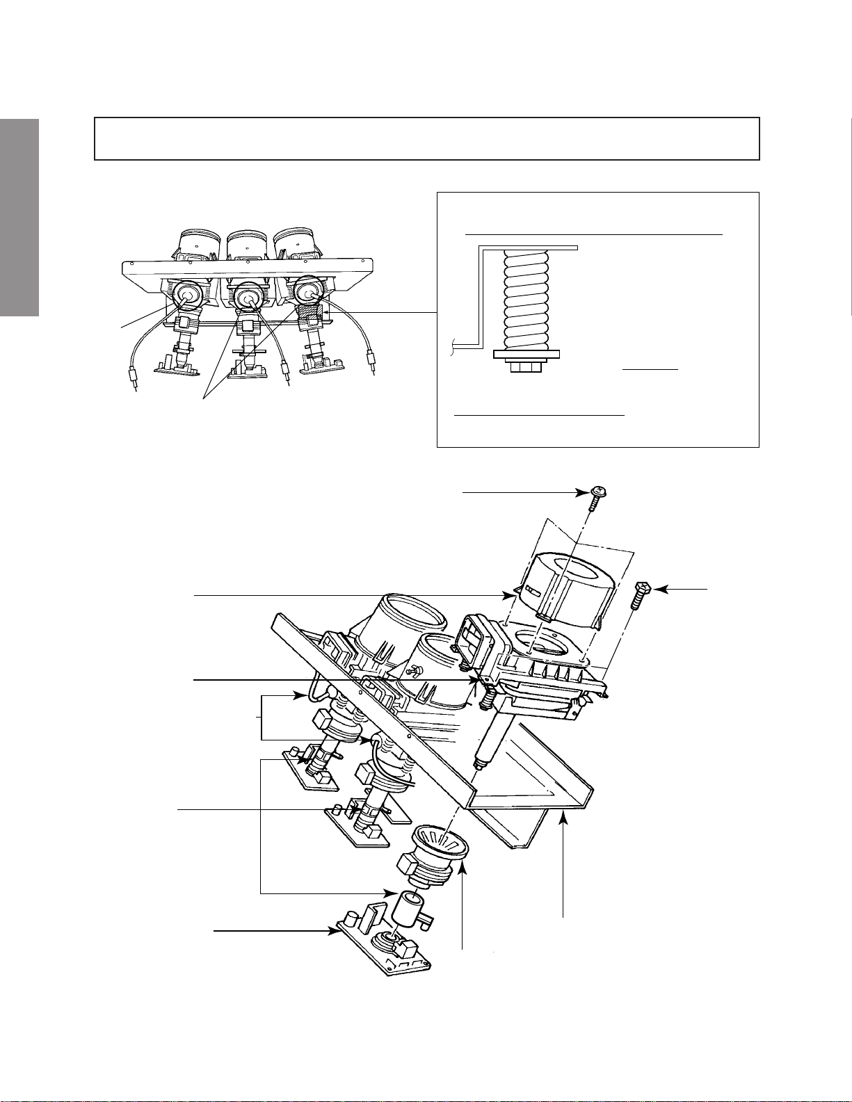
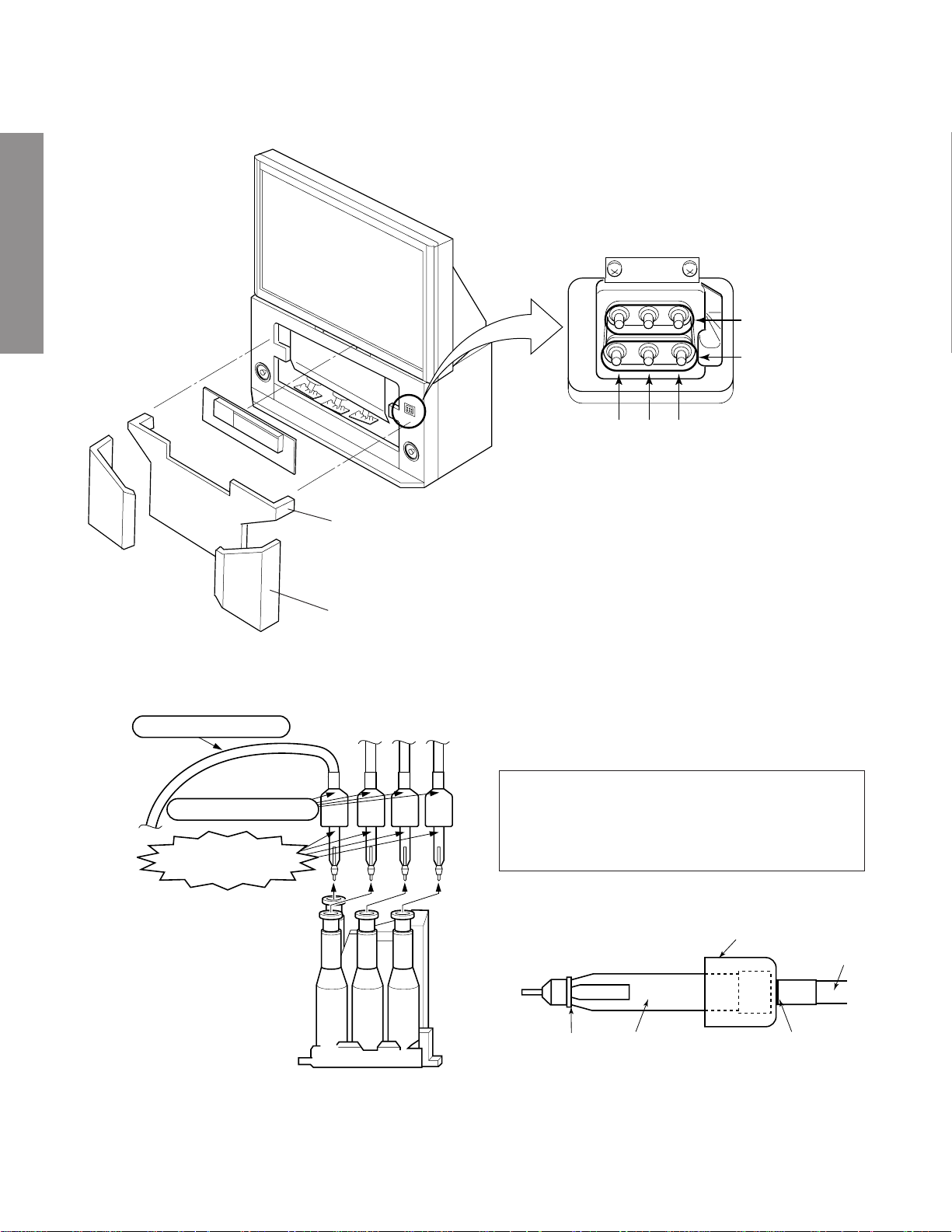
CRT ASSEMBLY REPLACEMENT AND MOUNTING
CAUTION : DO NOT LOOSEN THE HEX HEAD BOLTS WITH SPRINGS (12 PCS), BECAUSE THOSE ARE FOR
SEALING OF CRT COOLANT.
GENERAL ADJUSTMENTSSPECIFIC INFORMATIONS
8 o’clock
4 o’clock
Lens Assembly
R
GB
Attention Serviceman
The Hex Head
Bolts with
Springs. (see
sketch) used on
CRT assembly,
are “NOT”
Adjustment Screws
DO NOT LOOSEN-FLUID
LEAKAGE WILL OCCUR.
4 Screws
4 Screws
CRT Assembly
CRT Anode Cap Assembly
S.V.M. Coil
CRT DRIVE Board
CRT Mounting
Deflection Yoke and Conver Yoke
Lens and Neck Components View
– 4 –
Page 5
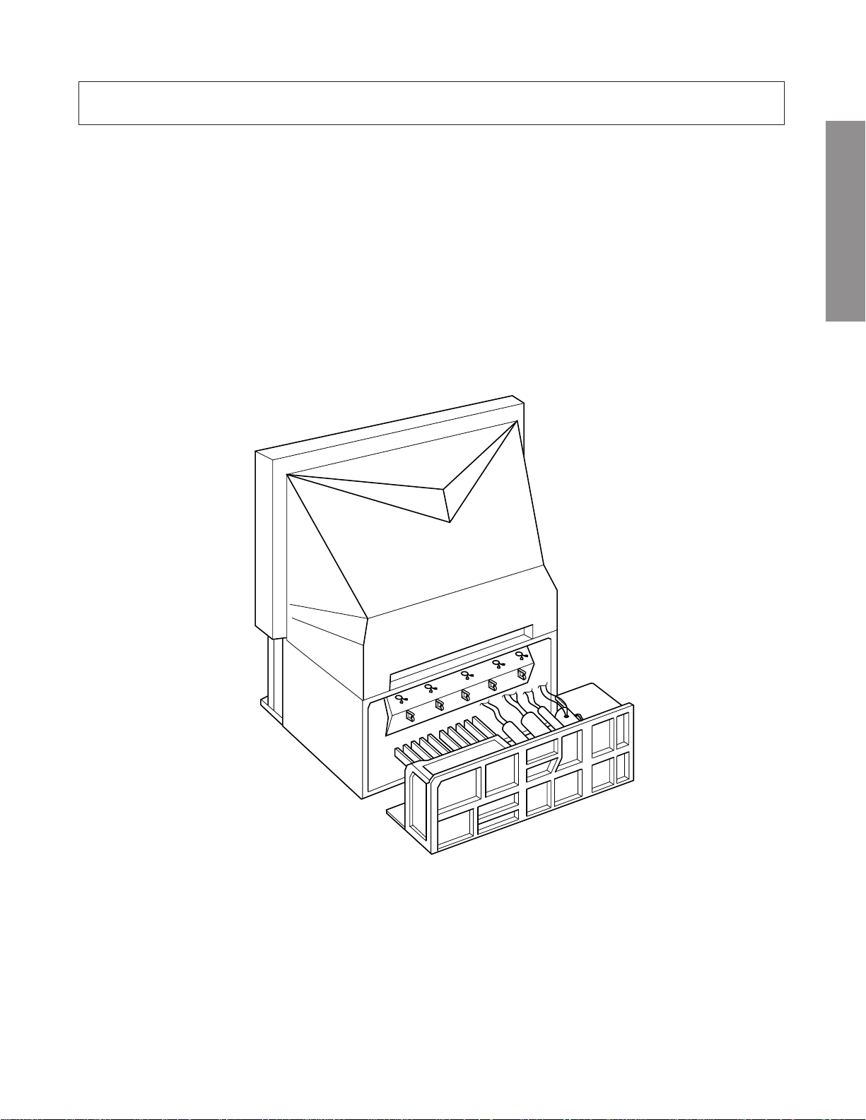
TO REMOVE CRT (Same procedure for R, G, B)
1. Remove CRT DRIVE Board, S. V. M. COIL and
DEF. YOKE from CRT.
2. Remove Lens Assembly.
3. Detach CRT Anode Cap from CRT.
4. Remove CRT Assembly from CRT Mounting.
CRT REPLACEMENT (Same procedure for R, G, B)
Reverse the removal procedures except the followings.
1. Anode Cable should be replaced with new one.
See "SERVICING PRECAUTIONS" shown below.
2. Install silicon (T461B) to the CRT, replace the Anode
cable and put enough silicon again on around the Anode Cap as illustrated.
CAUTION: Align the Anode cable as illustrated on page
4.
ADJUSTING PROCEDURE IN REPLACING CRT
1. R.G.B. CUTOFF (SCREEN VR) ADJUSTMENT (page 6.)
2. R.G.B. FOCUS ADJUSTMENT (page 6.)
3. PICTURE TILT ADJUSTMENT (page 7.)
4. USER CONVERGENCE CENTER CHECK
(Refer to owner's manual.)
5. CENTERING ADJUSTMENT (page 7.)
6. CONVERGENCE ADJUSTMENT (page 23.)
7. WHITE BALANCE ADJUSTMENT (page 15.)
Adjustments are complete.
Anode Cap
GENERAL ADJUSTMENTSSPECIFIC INFORMATIONS
Silicon
(On shaded area)
TSE3843W #23960136
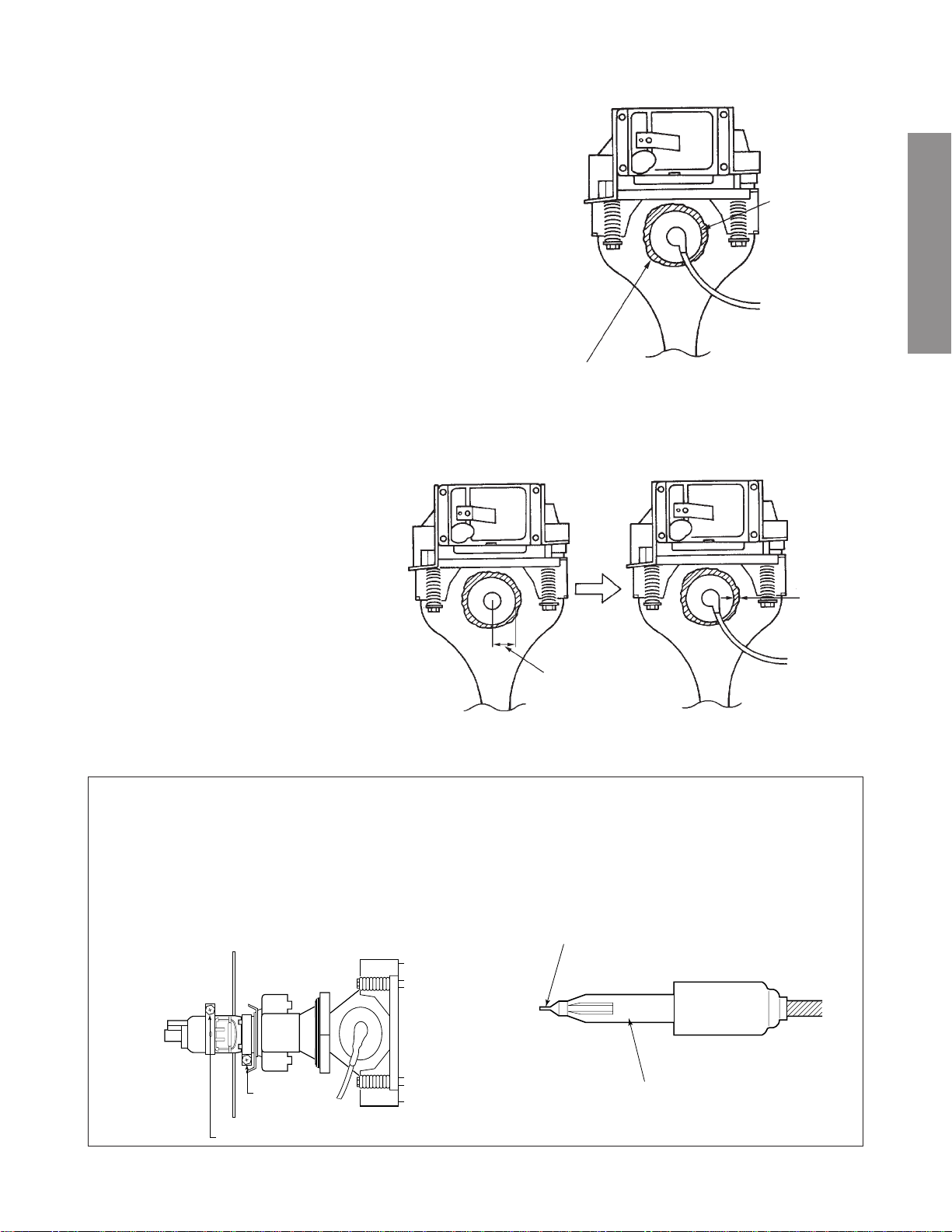
SERVICING PRECAUTIONS
■ Do not use a magnetized screw driver for screws
of Deflection Yoke and Velocity Modulation Coil to
avoid magnetization of electron gun.
Magnetization of electron gun will degrade basic
function and result in unbalance of right and left
shift of user static convergence, and result in no
variable quantity.
2 ~ 5 mm
15 ~ 25 mm
■ When replacing the anode cap assembly (CRT) or
anode lead assembly (F.B.T.), remove the anode
lead holder from old one and attach the holder
again to new anode lead.
■ Check the point of anode lead in a straight
line, if it is winding, please revise it.
Screw
for D.Y
Screw for SVM coil
Anode lead holder
– 5 –
Page 6
WARNING: BEFORE SERVICING THIS CHASSIS, READ THE "X-RAY RADIATION PRECAUTION", "SAFETY PRE-
CAUTION" AND "PRODUCT SAFETY NOTICE" ON PAGE 3 OF THIS MANUAL.
PICTURE TUBE COMPONENTS ADJUSTMENT
ADJUSTING PROCEDURE IN REPLACING CRT
Cutoff
Lens focus
Electrical focus
GENERAL ADJUSTMENTSSPECIFIC INFORMATIONS
Yoke horizontal
DESCRIPTION OF NECK COMPONENTS
S.V.M. COIL
1 Deflection yoke and convergence yoke.
The position on the neck is required most front (CRT funnel side) and the screw is fastened after rotating yoke
adjusting picture tilt.
2 Centering magnet
After adjusting picture tilt, picture position is finally fixed
by this magnet.
In order to get maximum margin of user convergence control for center of screen, this magnet have to be used for
center convergence adjustment.
2
User convergence center check
Centering (PAL)
Convergence adjustment
(PAL/NTSC)
White balance
Sub bright adjustment
End
1
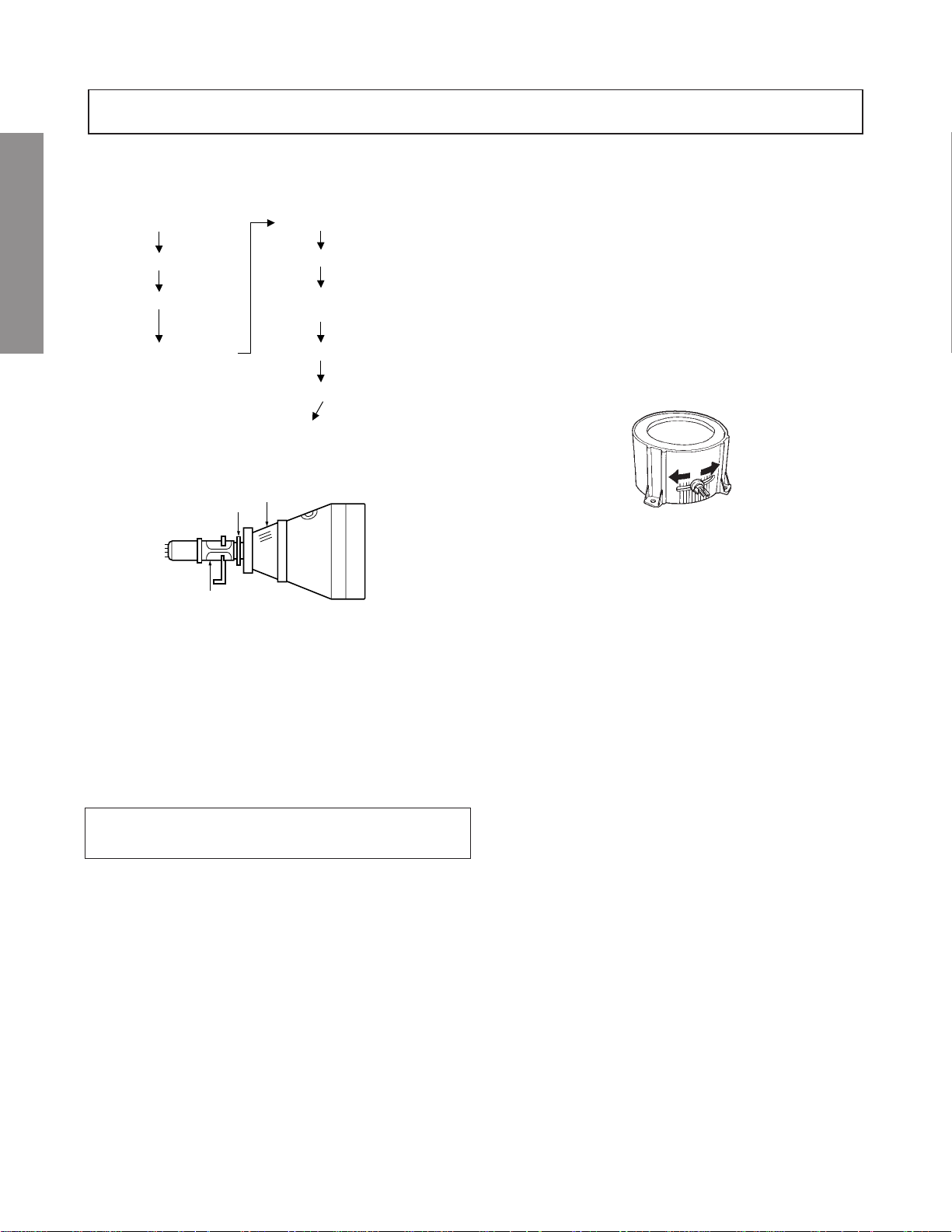
RGB FOCUS ADJUSTMENT
1. Call-up the adjustment mode (see page 10)
2. Press a b utton on the remote controller in order to display
the internally-generated cross-hatch (See TEST SIGNAL
SELECTION on page 11.)
3. Expose only RED by cover ing the GREEN and BLUE
lenses with caps.
4. Loosen the RED lens fixing screws (refer to Fig. a), and
adjust the RED lens focus to obtain the sharpest point
while observing the middle and peripheral sections of the
screen.
Fig. a
5. Use the focus VR of “R” of the focus pack in order to adjust
the electric focus in the middle and peripheral sections of
the screen to its sharpest level.
6. Check the RED focus of the whole screen and if necessary
repeat steps 4 and 5.
7. Fix the RED lens by tightening its fixing screws.
8. Expose only GREEN by covering the RED and BLUE
lenses with caps.
9. Display the internally-generated cross-hatch signal.
10. Adjust the GREEN lens focus on the left border of the
screen to its sharpest level, then check the focus on the
right border, and if it is at its sharpest level, fix it in that
position by tightening the lens screws.
PREPARATION
Operate the receiver for at least 5 minutes.
R, G, B CUTOFF (SCREEN VR) ADJUSTMENT
1. Adjust before replace the screen assembly.
2. Set user control to reset position.
CONTRAST → Max
(
BRIGHTNESS, COLOR, TINT → Center.
3. Call up the adjustment mode display, then select the
item RCUT.
4. Adjust the data of items RCUT, GCUT, and BCUT to
"40H".
5. Press the -/-- button on Remote. (Y-MUTE : ON)
6. Gradually rotate R, G and B screen volume of FOCUS
PAC clockwise or counterclockwise until the raster
appears slightly on the CRT through the each lens, and
leave them.
(Lookin to the lens in order to check the raster.)
7. Press the -/-- button on Remote. (Return to Normal
Picture)
(1) If the horizontal line toward the right border is red-
flared, turn the lens screw slightly right in order to
balance it with the left border. (After adjustment, the
left border tends to be slightly green-flared, and the
right border tends to be slightly red-flared.)
(2) If the horizontal line toward the right border is green-
)
Note: The aim of the above-described adjustment procedure
– 6 –
flared, turn the lens screw slightly left in order to
balance it with the left border. (After adjustment, the
left border tends to be slightly red-flared, and the
right border tends to be slightly green-flared.)
for the Green lens focus is to obtain the best lens focus
after 2 - 3 hours of warming up taking into account the
focus drift; it applies if the war ming up time before the
adjustment is less than 30 minutes. (The horizontal line
in the screen middle section tends to be slightly redflared.)
Page 7
In case of warming up of more than 2 hours under a condition
that the large anode current is running through the projection
tube so that for example the all-white pattern appears, adjust
to obtain the sharpest focus while observing the whole screen
like in the RED case.
11. Press a button on the remote controller in order to displa y
the internally-generated black cross-hatch. (See TEST
SIGNAL SELECTION on page 11.)
12. Use the focus VR of “G” of the focus pack in order to adjust the electric focus in the middle section of the screen
to its sharpest level.
Note: Keep in mind that only the BLUE electric focus is ad-
justed with the black cross-hatch.
20. Check the BLUE focus of the whole screen and if necessary repeat steps 17 and 19.
21. Fix the BLUE lens by tightening its fixing screws.
TILT ADJUSTMENT
Rotate R, G, B deflection yoke so that picture becomes horizon, then fasten screw.
CENTERING ADJUSTMENT
1. Stretch a thread between two center slots of screen edge
(top and bottom, left and right).
GENERAL ADJUSTMENTSSPECIFIC INFORMATIONS
Note: Nor mally the most clearly visible point of the scanning
line is the sharpest point of the Green focus, howev er as
the characteristics vary depending on the projection tube,
the sharpest focus points of the vertical and horizontal
lines may not match each other, thus when you turn the
focus VR, if the picture tends to be tremendously unstable
(rolls horizontally or vertically), adjust the balance of the
vertical and horizontal lines to its best position.
13. Check the GREEN focus of the whole screen and if
necessary repeat steps 10 and 11.
14. Fix the GREEN lens by tightening up its fixing screws.
15. Expose only BLUE by covering the RED and GREEN
lenses with caps.
16. Press a button on the remote controller in order to displa y
the internally-generated cross-hatch (See TEST SIGNAL
SELECTION on page 11.)
17. Loosen the BLUE lens fixing screws (refer to Fig. a), and
adjust the BLUE lens focus while observing the middle
and peripheral screen sections.
18. Press a button on the remote controller in order to displa y
the internally-generated black cross-hatch (See TEST SIGNAL SELECTION on page 11.)
19. Use the focus VR of “B” of the f ocus pack in order to adjust
the focus in the middle section of the screen to its sharpest
level.
(The point of the Blue focus becomes sharpest when the
brightness level of BLUE is lowest, the cross-hatch is
clearly visible.)
2. Select the adjustment mode. (See page 10.)
3. Press TV/VIDEO button on the Remote Control to display
the black cross-hatch.
4. Adjust G centering magnet so that the cross-hatch pat-
tern center comes to screen center.
5. Perform HEIGHT adjustment . (See page 14.)
6. Perform WIDTH adjustment. (See page 14.)
7. Check whole quality of green line.
8. Adjust R, B centering magnet so that the cross-hatch pat-
tern center comes to screen center.
– 7 –
Page 8
LOCATION OF SCREEN AND FOCUS VR'S
To remove the Speaker grille and Front panel.
GENERAL ADJUSTMENTSSPECIFIC INFORMATIONS
SCREEN VR
FOCUS VR
Front panel
Speaker grille
REPLACEMENT OF HIGH VOLTAGE CABLE
ANODE LEAD
RUBBER BOOT
LEAD HOLDER
B
1. When replacing Anode Lead or Anode Cap with new
one, remove Lead Holder from old lead as shown in
figure below , and put it on new lead. Do not throw awa y
Lead Holder.
NOTE : THE LEAD HOLDER IS ATTACHED TO
TP A5007 (Z450), BUT IS NO T A TTACHED TO
ANODE LEAD AND ANODE CAP. RUBBER
BOOT IS ATTA CHED TO ANODE LEAD AND
ANODE CAP.
RG
Fig. a
Z450 TPA5007
– 8 –
2. Detaching Lead Holder
LOCK
LEAD HOLDER
RUBBER BOOT
Fig. b
OLD
ANODE LEAD
or
ANODE CAP
Cut here rubber boot
and lead together to
detach Lead Holder.
Page 9
WARNING: BEFORE SER VICING THIS CHASSIS , READ THE "X-RAY RADIA TION PRECA UTION", "SAFETY PRECAU-
TION" AND "PRODUCT SAFETY NOTICE" ON PAGE 3 OF THIS MANUAL.
SERVICE POSITION
In order to assure the performance, processed wires shall be replaced after the repair work.
Work procedures are as follows:
1. Remove the back board.
2. Remove lead wires.
3. Draw out the chassis.
4. Rest the chassis against the back cabinet, chassis as shown bellow.
After repair work finished, replace it in the opposite procedure.
GENERAL ADJUSTMENTSSPECIFIC INFORMATIONS
– 9 –
Page 10
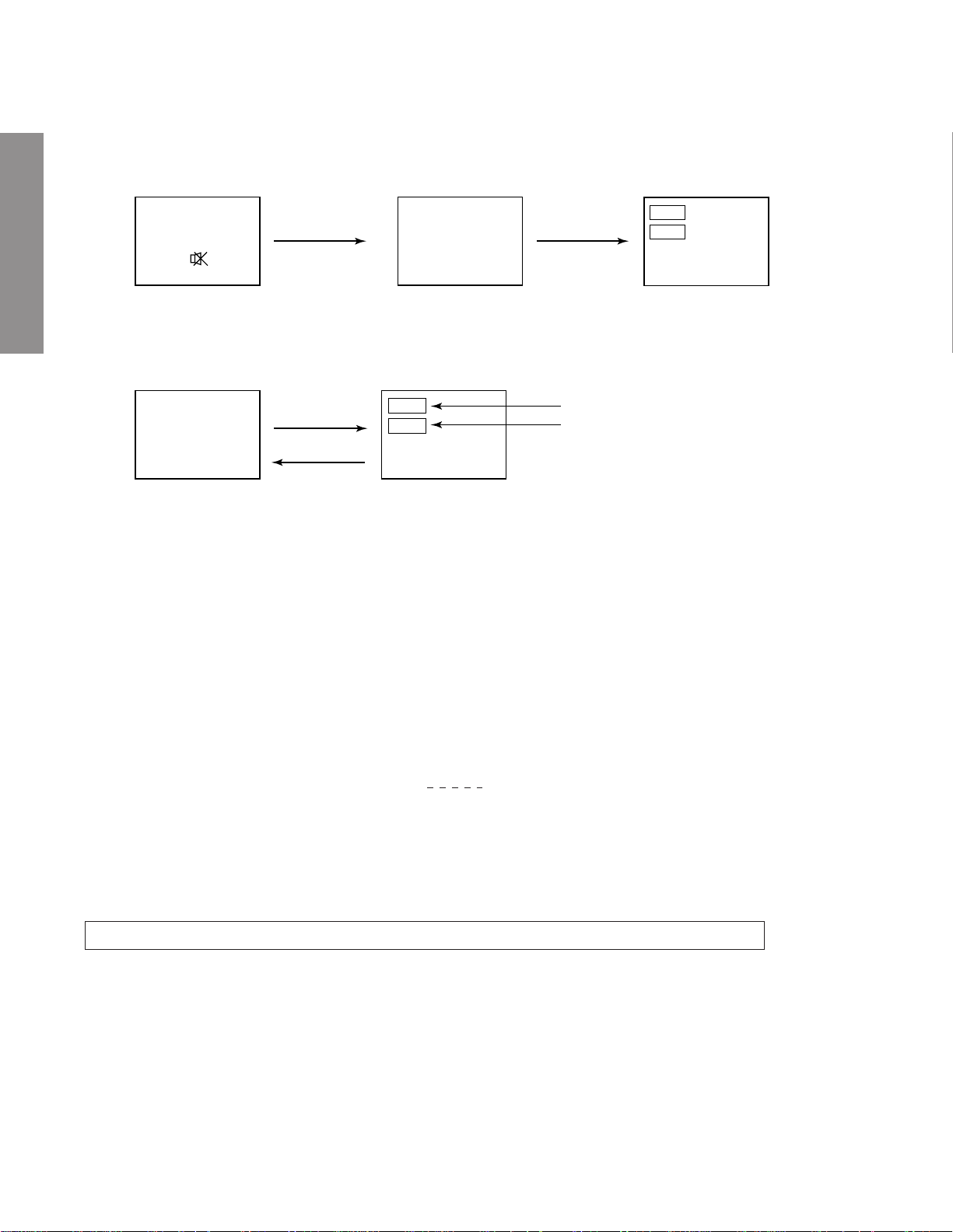
1. ENTERING TO SERVICE MODE
1) Press o button once on
Remote Control.
SERVICE MODE
2) Press o button again to
keep pressing.
3) While pressing the o button,
press MENU button on TV set.
or Sound Mute
GENERAL ADJUSTMENTSSPECIFIC INFORMATIONS
2. DISPLAYING THE ADJUSTMENT MENU
1) Press MENU button on TV.
Service mode
3. KEY FUNCTION IN THE SERVICE MODE
The following key entry during display of adjustment menu provides special functions.
Screen adjustment mode ON/OFF: -/-- button (on Remote)
Test signal selection : a button (on Remote)
Selection of the adjustment items : Channel s/t (on TV or Remote)
Change of the data value : Volume ; +/– (on TV or Remote)
Adjustment menu mode ON/OFF : MENU button (on TV)
Initialization of the memory (QA02) : CALL + Channel button on TV (s)
Reset the count of operating protect
circuit to “00”: CALL + Channel button on TV (t)
“RCUT” selection : 1 button
“GCUT” selection : 2 button
“BCUT” selection : 3 button
“SCNT” (or “CNTX”) selection : 4 button
“COLC” (or “SCOL”) selection : 5 button
“TNTC” selection : 6 button
Convergence adj : YELLOW button
Self diagnostic display ON/OFF : 9 button
Item
Data
(Service mode display)
Adjustment mode
S
Press
Press
Item
Data
S
Color thickness correction
note: Displayed differently as shown below, de-
pending on the setting of the receiving color
system.
COLP (PAL)
COLC (NTSC)
COLS (SECAM)
CAUTION : Never try to perform initialization unless you have changed the memory IC.
– 10 –
Page 11
4. SELECTING THE ADJUSTING ITEMS
1) Every pressing of CHANNEL s button in the service mode changes the adjustment items in the order of table-2.
(t button for reverse order)
Refer to table-2 for preset data of adjustment mode.
(See SETTING & ADJUSTING DATA on page 34)
5. ADJUSTING THE DATA
1) Pressing of VOLUME ; +/– button will change the value of data in the range from 00H to FFH. The variable
range depends on the adjusting item.
6. EXIT FROM SERVICE MODE
1) Pressing POWER button to turn off the TV once.
■ INITIALIZATION OF MEMORY DATA OF QA02
After replacing QA02, the following initialization is required.
1. Enter the service mode, then select any register item.
2. Press and hold the CALL button on the Remote, then press the CHANNEL s button on the TV. The initialization of QA02 has
been complated.
3. Check the picture carefully. If necessary, adjust any adjustment item above.
Perfor m “Auto search Memory” on the owner’s manual.
CAUTION: Never attempt to initialize the data unless QA02 has been replaced.
7. TEST SIGNAL SELECTION
1) Every pressing of a button on the Remote Control changes the built-in test patterns on screen as described below
in SERVICE MODE.
Signal off
NTSC signals (5 patterns)
PAL signals (5 patterns)
Signals Picture
• Red raster
• Green raster
• Blue raster
• All White
• Black cross-hatch
GENERAL ADJUSTMENTSSPECIFIC INFORMATIONS
The signals marked with are not usable to display in the Test signal for some model.
*
– 11 –
Page 12

8. SELF DIAGNOSTIC FUNCTION
1) Press “9” button on Remote Control during display of adjustment menu in the service mode.
The diagnosis will begin to check if interface among IC’s are executed properly.
2) During diagnosis, the following displays are shown.
<SELF CHECK>
1
2300****
2
POWER : 00
3
BUS CONT : OK
4
BLOCK : UV V1 V2 V3
QV01
GENERAL ADJUSTMENTSSPECIFIC INFORMATIONS
Indicated color of mode now selected : Green and Red
Indicated color of other modes : White
Green :Normal
Red : The microcomputer operates to provide judgement
of no video signal. The red color is still indicated
though the signal is input, failure may e xist in input
signal line including QV01.
QV01 : In case of indication green ---Normal
In case of indication red with input signal---Failure may exist in output line including QV01.
1 Part number of microcomputer (QA01)
2 Operation number of protecting circuit ----“00” is nor-
mal.
When indication is other than “00”, overcurrent apts to
flow, and circuit parts may possibly be damaged.
3 BUS CONT ----“OK” is normal.
When indication shows “Q uuu (Green: OK, Red:
NG)”, the device with the number ma y possibly be damaged.
NOTE: Component which controls character display on
screen is QT01 (TELETEXT IC.). If this display
function fails to operate due to damage in QT01,
self diagnosis procedure is as follows.
(1) In case that on timer indicator is blinking with
interval of 0.5 seconds; it means protecting circuit (Current limiter) is operating, and circuit
components may possibly be damaged. Check
related components.
4 BLOCK
UV : TV reception mode
V1 : VIDEO 1 input mode (a1)
V2 : VIDEO 2 input mode (a2)
V3 : VIDEO 3 input mode (a3)
The items marked with are not usable to display in the SELF DIAGNOSTIC FUCTION for some model.
*
– 12 –
Page 13

1. ENTERING TO DESIGN MODE
1) Select the Service mode.
DESIGN MODE
2) While pressing CALL button on Remote
and press MENU button on TV.
3) Press MENU button on TV.
S D
(Design mode) (Adjustment mode)
When QA02 is initialized, items “OPT0” and “OPT1” of DESIGN MODE are set to the data of the representative model of this
chassis family.
Therefore, because ON-SCREEN specification remains in the state of the representative of model. This model is required to
reset the data of items “OPT0” and “OPT1”.
2. SELECTING THE ADJUSTING ITEMS
Every pressing of CHANNEL t button in the design mode changes the adjustment items in the order of table-3.
(s button for reverse order)
Refer to table-3 for data of design mode.
(See SETTING & ADJUSTING DATA on page 34)
3. ADJUSTING THE DATA
Pressing of VOLUME s or t button will change the value of data.
Press
Press
ITEM
DATA
GENERAL ADJUSTMENTSSPECIFIC INFORMATIONS
– 13 –
Page 14

PAL
ELECTRICAL ADJUSTMENT
ITEM ADJUSTMENT PROCEDURE
WIDTH
(WID)
GENERAL ADJUSTMENTSSPECIFIC INFORMATIONS
HEIGHT
(HIT)
1. Select picture size WIDE mode.
2. Call up the adjustment mode display, and press the TV/VIDEO
button on the remote untill the white cross dot pattern appears on
the screen.
3. Press the CHANNEL s or t button to select the item WID and
press the VOLUME s or t button to get the pictuer so the left and
right edges of rester begin to lack.
4. Press the VOLUME s or t to advance the data 22 steps.
* CAUTION
"WID" data don't adjust other picture size, only WIDE mode.
1. Call up the adjustment mode display, then select the item HIT.
2. Press the VOLUME s or t button to get the picture so the top of
raster begins to lack.
3. Press the VOLUME s button to advance the data by following steps.
WIDE: 7 steps
Super Live: 11 steps
CINEMA: 10 steps
* CAUTION
First adjust WIDE mode next other.
Note : Check the vertical picture position is correct.
NTSC
WIDTH
(NWID)
HEIGHT
(NHIT)
1. Select picuter size wide mode.
2. Call up the adjustment mode display, and press the TV/VIDEO
button on the remote untill the white cross dot pattern appears on
the screen.
3. Press the CHANNEL s or t button to select the item WID and
press the VOLUME s or t button to get the pictuer so the left and
right edges of rester begin to lack.
4. Press the VOLUME s or t to advance the data 16 steps.
5. Change picture size Super Live and CINEMA adjust "NWID" data
same value for WIDE mode.
1. Call up the adjustment mode display, then select the item HIT.
2. Press the VOLUME s or t button to get the picture so the top of
raster begins to lack.
3. Press the VOLUME s button to advance the data by following steps.
WIDE: 7 steps
Super Live: 13 steps
CINEMA: 10 steps
Note : Check the vertical picture position is correct.
– 14 –
Page 15

ITEM ADJUSTMENT PROCEDURE
WHITE BALANCE
(RCUT)
(GCUT)
(BCUT)
(RDRV)
(BDRV)
Black and White pattern
High light area
Adjust "RDRV" or "BDRV" to be white.
Low light area
Fine adjust "RCUT", "GCUT" or "BCUT" to be black.
1. Set user control to reset position.
CONTRAST → Min.
(
BRIGHTNESS, COLOR, TINT → Center.
2. Call up the adjustment mode display, then select the item RCUT.
3. Adjust the data of items RCUT, GCUT, and BCUT to "40H".
4. Press the a button on PJTV. (Y-MUTE : ON)
5. Gradually rotate R, G and B screen volume of FOCUS PAC clockwise or
counterclockwise until the raster appears slightly on the CRT through the
each lens, and leave them.
(Lookin to the lens in order to check the raster.)
6. Press the a button on PJTV. (Return to Normal Picture)
7. Press the a button on Remote, and select the Black and White pattern.
8. Adjust the data of items RCUT, GCUT and BCUT for proper white-balanced
picture in low light area.
9. Adjust the data of items RDRV and BDRV for proper white-balanced picture in
high light area.
10. Check the white balance in both low and high light areas.
If necessary, perform again steps from 8 to 9.
)
GENERAL ADJUSTMENTSSPECIFIC INFORMATIONS
– 15 –
Page 16

GENERAL ADJUSTMENTSSPECIFIC INFORMATIONS
2.4 ± 0.1 Vpp
y Adjust the amplitude from the pedestal
4 ± 1.5 linee
level to the white peak.
lines of the sub-bright signal.
y Adjust the number of collapsed black
1.30 ± 0.1 Vpp
W/B and SCNT.
x Carry out adjustment after adjusting the
y Adjust the amplitude of the color bar.
100 ± 10 %
the waveforms can become flat.
x Adjust the P-P value of the upper half.
y Use a synchroscope and adjust so that
x Adjust at the white part.
1.95 ± 0.1Vop
(Apply SCREEN mute during adjust-
ment)
y Adjust the amplitude of the color bar.
0 ± 10 mV
chrome signal part can meet the level of
x Adjust the P-P value of the upper half.
y Adjust so that the level of the mono-
0 ± 10 mV
the H.BLK.
BELL.
chrome signal part can meet the level of
the H.BLK.
BELL.
x Carry out adjustment after adjusting the
y Adjust so that the level of the mono-
x Carry out adjustment after adjusting the
TP46B SIGNAL unit
Sub-bright signal
Dynamic mode
Sub-contrast
Screen adjustment
(PAL-I signal)
Sub-bright signal
Audio system: I
Dynamic mode
Sub-bright
center
TP46B
SIGNAL unit
TPM01
SIGNAL unit
Sub-bright signal
(PAL)
SECAM color bar
Dynamic mode
Sub-color
center
PAL
BELL filter
TP46B
SIGNAL unit
SECAM color bar
Dynamic mode
Sub-color
center
TP02
SECAM color bar
Dynamic mode
SECAM
SECAM
SIGNAL unit
R-Y black level
TP01
SIGNAL unit
SECAM color bar
Dynamic mode
SECAN
B-Y black level
Item Name Setting Input signal Measuring point Adjusting method Adjustment standard
(Reference factory adjustment)
[SCNT]
[BRTC]
[COLP]
[BELL]
– 16 –
[COLS]
[SRY]
[SBY]
Page 17

Point where it
begins to emit light.
For details, refer to
the focus adjust-
ment method
introduced in the
next page.
8750k–0.002uv
8750k–0.002uv
30.7 ± 0.2kV
possible.
x Enter factory-screen-adjustment mode.
y Make the surrounding as dark as
CRT screen
(Y mute, DRV.CUT. = 40 H)
adjust the screen VR to the point where
it begins to emit light.
perform above-mentioned adjustments.
c Directly observe the CRT screen, and
v Use R, G, and B tubes respectively to
possible position by repeating electrical
y Make adjustments to achieve the best
Crosshatch signal
Screen adjustment
Retoma signal
(PAL-I)
axis under adjustment, from any light.
and optical focusing.
x Use jigs to protect the CRTs, except the
c Use R, G, ad B tubes respectively to
).
2
perform above-mentioned adjustments.
bright part (103cd/m
y Adjust the color temperature of the
y Adjust the color temperature of the dark
Screen adjustment
Screen adjustment
).
2
part (17cd/m
y Connect a voltmeter between T461 and
Between T461 and
Phillips pattern
Z450 and adjust the high voltage with
R450.
(User adjustment standard)
Z450
(PAL-I)
GENERAL ADJUSTMENTSSPECIFIC INFORMATIONS
Factory- screen-
adjustment mode
Screen
Item Name Setting Input signal Measuring point Adjusting method Adjustment standard
Screen
adjustment
Dynamic mode
Cinema mode
Focus
Focus
adjustment
– 17 –
Bright part W/B
RDRV
BDRV
Dark part W/B
RCUT
BCUT
Dynamic mode
High voltage
High voltage
adjustment
Page 18
GENERAL ADJUSTMENTSSPECIFIC INFORMATIONS
Focus adjustment method (1/2)
(2) GREEN: Internal crosshatch signal (white crosshatch on black background)
(3) User adjustment: Dynamic mode, cinema mode
Conditions: (1) RED, BLUE: Internal Retoma signals (PAL)
(4) Carry out electrical focus and lens focus after rough adjustment.
(5) Use the jig to protect everything, except the color subjected to adjustment, from exposure to light.
each R and B projection tube to the position where the center of the screen gets optimally focused.
G so that the vertical scanning lines on the screen center can appear most clearly.
best possible focus.
(1)Receive the internal Retoma signals, use the focus VR of the focus pack (Z410), and adjust the electrical focus of
(2)Receive the internal crosshatch signals, use the focus VR of the focus pack (Z410), and adjust the electrical focus of
(1)R, B: Receive the internal Retoma signals, watch the screen center and its periphery, and make adjustment to the
(2)G: Adjust this by the method introduced in the next page.
set on the screen.
until immediately before the cutoff adjustment in order to stabilize the G’s coupling liquid temperature.
y Carry out anticipated adjustment on the G lens, considering the time until the lens focus stabilizes.
x The level of anticipated adjustment on the G lens results in a required level of correction, if an adjustment point is
c During a heat run, be sure to keep lower the G’s screen VR of the focus pack from turning on the power of the set
Model Adjustment points Adjustment methods
40PW03G
40PW03B
Electrical focus
– 18 –
Lens focus
(Precautions)
Page 19
GREEN lens focus adjustment
Focus adjustment method (2/2)
GENERAL ADJUSTMENTSSPECIFIC INFORMATIONS
the very best, and check that the left-and-right focus balance is appropriate.
(Check left-and right balance of G lens focus)
(2)Watch the horizon of both the left and right ends on the horizontal axis of the screen, adjust the lens focus of G to
Screen
Model Metodo di regolazione
Adjusting points
[1] 40PW03 series (1)Receive internal crosshatch signals, use the lens cap, and concentrate on the single color of G.
y Use the left (or right) end crosshatch and make the best adjustment on the G’s lens focus.
x Check the right (or left) end focus.
(3)If the left and right lens focus is not properly balanced (tendency for flare), divide and adjust it to the middle grade.
(4)Check on the periphery, and make certain that the focus grade lies within a tolerable level (including flare).
Right end
Left end
– 19 –
ø 100 mm ø 100 mm
(Point of observation)
Inside the circle of 100mm that is in contact with
left and right bezels.
Page 20

GENERAL ADJUSTMENTSSPECIFIC INFORMATIONS
Less than ø7mm
Adjustment standard
screen positions and centering magnet
so that the central + mark of the dummy
screen and the + mark of the Phillips
pattern can overlap in conformity.
(1)Adjust the vertical and horizontal
Upper and lower
flags are to be in
contact
Carry this out individually on 3 tubes of
R, G, and B
(Note) Do not move HPOS, VPOS data
amplitude using HIT data until the upper
and low flags emerge on the screen.
the HIT data until either upper or lower
flag end conforms to the screen end
(Adjust the vertical center of the pattern
to the central mark of the screen.)
(1)Turn the screen size to WIDE.
(2)In the first place, shorten the vertical
(3)Then, extend the vertical amplitude with
The inner circle is
to contact the
screen edge
bottom of the inner circle of Phillips
pattern will contact the screen edge.
(Note) VLIN adjustment is not performed.
(1)Turn the screen size to Super-live.
(2)Adjust with the HIT so that the top and
bottom of the Phillips pattern as shown
in the next page.
(1)Turn the screen size to CINEMA.
(2)Adjust the registers on the top and
(Note) Do not touch the centering magnet
Screen adjustment
Screen adjustment
Completion of adjustment
Phillips pattern
(PAL-I)
Dynamic mode
Phillips pattern
(PAL-I)
Dynamic mode
WIDE mode
Vertical ampli-
tude adjustment
(PAL WIDE)
Screen adjustment
Phillips pattern
(PAL-I)
Dynamic mode
Super-live mode
Vertical ampli-
tude adjustment
(PAL Super-live)
Screen adjustment
Phillips pattern
Dynamic mode
Vertical ampli-
(PAL-I)
CINEMA mode
tude adjustment
(PAL cinema)
Item Name Setting Input signal Measuring point Adjusting method
Screen
position
adjustment
HIT
VLIN
– 20 –
HIT
VLIN
HIT
VLIN
Page 21

Adjustment standard
bottom of the Phillips pattern as shown
in the next page.
(1)Turn the screen size to SUB-TITLE.
(2)Adjust the registers on the top and
(Note) Do not touch the centering magnet
pattern are to contact the screen edge.
be 0.
(1)Turn the screen size to WIDE.
(2)The left and right flags of the Phillips
(3)The user center position adjustment is to
(1)Turn the screen size to WIDE mode.
(2)The 1st line on the screen is to be
hidden by the mask.
mode.
(1)Turn the screen size to SUPER-LIVE
(2)Adjust so that the upper side 3rd line on
the screen will contact the screen edge.
(3)Do not adjust the NVLI.
upper, lower, and left-and-right ends will
contact the screen edge.
(1)Turn the screen size to CINEMA mode.
(2)Adjust so that the character 30 on the
mode.
the register on the screen will contact the
screen.
(1)Turn the screen size to SUB-TITLE
(2)Adjust so that the upper side 5th line of
(3)The NVLI is not to be adjusted.
GENERAL ADJUSTMENTSSPECIFIC INFORMATIONS
Screen adjustment
Screen adjustment
Completion of adjustment
Phillips pattern
(PAL-I)
Dynamic mode SUB-
TITLE mode
Vertical ampli-
tude adjustment
(PAL SUB-
TITLE)
Phillips pattern
(PAL-I)
Dynamic mode
WIDE mode
Vertical ampli-
tude adjustment
PAL WIDE
Screen adjustment
Monosco signals
Dynamic mode
Vertical ampli-
Screen adjustment
NTSC
LEADERE-435B
Monosco signals
NTSC
LEADER-435B
WIDE mode
Dynamic mode
SUPER-LIVE mode
tude adjustment
NTSC WIDE
Vertical ampli-
tude adjustment
SUPER-LIVE
Screen adjustment
Monosco signals
NTSC
Dynamic mode
CINEMA mode
NTSC
Vertical ampli-
tude adjustment
Screen adjustment
LEADER-435B
Monosco signals
NTSC
LEADER-435B
Dynamic mode
SUB-TITLE mode
CINEMA
NTSC
Vertical ampli-
tude adjustment
SUB-TITLE
NTSC
Item Name Setting Input signal Measuring point Adjusting method
HIT
VLIN
WID
NHIT
NLIN
– 21 –
NHIT
NHIT
NLIN
NHIT
NLIN
Page 22

GENERAL ADJUSTMENTSSPECIFIC INFORMATIONS
Adjustment standard
edge of the screen.
the WIDE screen also input the identical
(2)Adjust the 2nd left register to the left
(3)When you change the NWID value on
Adjustment standard
data to SUPER-LIVE and CINEMA.
32 ± 0.1 MHz
+9V to #13 terminal
–9V to #14 terminal.
L719.
(2)Adjust emitter’s frequency to Q709 with
Screen adjustment (1)Turn the screen size to WIDE.
Completion of adjustment
Monosco signals
NTSC
LEADER-435B
Dynamic mode
WIDE mode
amplitude
adjustment
WIDE NTSC
Q709 Emitter (1)Apply +5V to #15, #16 terminals
Unit adjustment DIGITAL-CONVER
Item Name Setting Input signal Measuring point Adjusting method
NWIDE Horizontal
– 22 –
Item Name Setting Input signal Measuring point Adjusting method
PLL
Frequency
adjustment
Page 23
CONVERGENCE ADJUSTMENT
1. Screen Adjustment
The four PAL screens Wide/4:3, Super Live, Cinema and Subtitle, and the four NTSC screens Wide/4:3, Super Live,
Cinema and Subtitle are adjusted. When adjusting, input an external signal for matching the sync.
CAUTION: The con vergence circuit eliminates screen distortion but cannot make large corrections such as changing
the overall screen size. Use caution because the protection circuit will be activated if corrections are excessively
large. Before starting to adjust the various screens, alw ays adjust the v ertical size (HIT) and horizontal size (WID) b y
changing the main deflection data.
Execute the adjustment screens in the sequence Wide/4:3 → Super Live → Cinema → Subtitle for both PAL and
NTSC.
1-1. Entering Adjustmet Menu
GENERAL ADJUSTMENTSSPECIFIC INFORMATIONS
+ + MENU key
F+Yellow key
Menu screen
CONVER ADJUST MENU
1
Adjust PAL Wide
2
PAL Wide to Others
3
Adjust PAL S.Live
4
Adjust PAL Cinema
5
Adjust PAL S.title
6
PAL to NTSC (Wide)
7
PAL to NTSC (ALL)
8
Adjust NTSC Wide
9
NTSC Wide to Others
10
Adjust NTSC S.Live
11
Adjust NTSC Cinema
12
Adjust S.title
S
Service data indication
+
or
MENU SELECTION
+ key
SCREEN
ADJUSTMENT
CALL: to exit
Adjusting screen
+ key
– 23 –
Page 24
1-2. Remote Control Key
b
h
GENERAL ADJUSTMENTSSPECIFIC INFORMATIONS
i
g
j
F
1
2
f
Çi
CALL
3
TEXT
4 5 6
7 8
-/--
v
SIZE
MENU EXIT
0
?
ENTER
SELECT
9
a
^
CH
yX
V
l
p
k
c
a o key............... Push this key twice and the set con-
sole menu key to enter the service
mode.
b F key................. Push this key and yellow key to enter
the convergence menu.
c Yellow or 7 key.. Convergence menu key.
g 5 key................. Cursor shift / data change mode
change-over.
h 2 key................. Cursor up / adjusting point up.
i 4 key................. Cursor left / adjusting point left
j 8 key................. Cursor down / adjusting point down
k 6 key................. Cursor right / adjusting point right
l 3 key................. Cursor colour change (Adjusting
colour selection).
m + key................. Execution key on conv ergence menu.
n s key ................ Up key on convergence menu.
o t key ................ Down key on convergence menu.
p CALL key .......... Termination key on convergence
menu.
n
o
REC
a
m
P
VTR/DVD
Fig. 2
– 24 –
Page 25

1-3. Adjusting Screen
1) Adjusting menu
NO Description
1 Adjust PAL Wide Used for manual adjustment of the Wide/4:3 screen in the PAL mode.
2 P AL Wide to others Automatically sa ves approximate supplementary data f or the other P AL screens based
3 Adjust PAL S.Live Used for manual adjustment of the PAL Super Live screen.
4 Adjust PAL Cinema Used for manual adjustment of the PAL Cinema screen.
5 Adjust PAL S.title Used for manual adjustment of the PAL S.title screen.
Item
Returns to the original screen data screen before data conversion, explained below.
on the PAL Wide/4:3 screen data.
First, the PAL Wide/4:3 screen data are converted to Super Live and the values are
saved. Next, the data are converted to Cinema and the values are saved. Finally, the
data are converted to Subtitle and the values are sav ed, and then the operation ends .
Manually check the other screen modes as described below and make corrections if
distortion, etc., is present.
Please be aware that all PAL screens are re-adjusted when this menu is selected and
executed.
Select this mode for Super Live screen color matching and distortion adjustment.
Use the specified dimensions when adjusting.
Select this mode for Cinema screen color matching and distortion adjustment.
Use the specified dimensions when adjusting.
Select this mode for S.title screen color matching and distortion adjustment.
Use the specified dimensions when adjusting.
GENERAL ADJUSTMENTSSPECIFIC INFORMATIONS
6 PAL to NTSC (Wide) PAL Wide/4:3 screen data is calculated, converted to NTSC Wide/4:3 approximate
data and saved.
To assure accurate adjustments, select the manual mode explained below and chec k,
then apply color matching and distortion adjustments.
7 PAL to NTSC (All) Data for all PAL screens is converted to approximate data for the NTSC screens and
saved.
To assure accurate adjustments, select the manual mode explained below and chec k,
then apply color matching and distortion adjustments.
8 Adjust NTSC Wide Used for manual adjustment of the NTSC Wide/4:3 screen.
Select this mode for Wide/4:3 screen color matching and distortion adjustment.
Use the specified dimensions when adjusting.
9 NTSC Wide to others Approximate supplementary data for the other NTSC screens is automatically saved
based on the NTSC Wide/4:3 screen data.
First, the NTSC Wide/4:3 screen data are converted to Super Live and the values are
saved. Next, the data are converted to Cinema and the values are saved. Finally, the
data are converted to Subtitle and the values are sav ed, and then the operation ends .
Manually check the other screen modes as described below and make corrections if
distortion, etc., is present.
Please be aware that all NTSC screens are re-adjusted when this menu is selected
and executed.
– 25 –
Page 26
NO Description
10 Adjust NTSC S.Live Used for manual adjustment of the NTSC Super Live screen.
11 Adjust NTSC Cinema Used for manual adjustment of the NTSC Cinema screen.
12 Adjust NTSC S.title Used for manual adjustment of the NTSC Subtitle screen.
GENERAL ADJUSTMENTSSPECIFIC INFORMATIONS
2) Adjustment Screen
Item
Select this mode for Super Live screen color matching and distortion adjustment.
Use the specified dimensions when adjusting.
Select this mode for Cinema screen color matching and distortion adjustment.
Use the specified dimensions when adjusting.
Select this mode for Subtitle screen color matching and distortion adjustment.
Use the specified dimensions when adjusting.
X : 1
Y : 1
C : R
S : 08
Wide
Displayed when the cursor blinks and cleared
when the cursor lights steady.
X Cursor horizontal position display
Displayed when the cursor blinks and
cleared when the cursor lights steady.
Displays the current screen mode.
Y Cursor vertical position display
C Cursor color select display
S Menu select display
3) Adjustment Sequence
When the initial screen opens, X = 1, Y = 1, C = R and S = [Select Menu] are displayed as the defaults. The cursor can
now be moved up, down, left and right using the (2), (8), (4) and (6) keys of the remote control. Select the desired
adjustment and press the (5) key; the cursor will light steady and the screen display will be cleared. Again press the (2),
(8), (4) and (6) keys of the remote control to adjust the shape of the screen. When adjustment has been completed, press
the (+) key to return to the Adjustment Menu. When all of the screen adjustments have been completed, turn off the main
power supply of the set to reset the menu.
– 26 –
Page 27

2. Case Study
In many cases, color matching problems can be solved by retur ning the HIT and WID data for main deflection to the
initial adjustment values. Convergence cannot be re-adjusted in the following cases.
2-1 When the CRT has been replaced
Main deflection re-adjustment and color matching are necessary when the CRT has been replaced. Use the following
procedure.
1. Replace the blue and red CRTs.
2. Perform the blue and red yoke horizontal adjustments in relation to the green CRT. Press the yokes and speed
modulation coils + alignments onto the CRTs and fasten after making sure that there are no gaps.
3. Adjust the blue and red alignments (refer to the detailed alignment adjustment item).
4. Use centering magnets to center the blue and red CRTs in relation to the green CRT.
5. Adjust the main deflection HIT and WID data, using the most accurate location in relation to the green as data.
6. Use convergence to match the colors for each screen. Green will not work at this time.
7. When the convergence adjustments have been completed for all screens, then replace the green CRT.
Repeat the procedures in steps 2 - 5 for the green CR T but this time use con vergence to match the colors using red and
blue as reference.
2-2 When replacing the convergence unit
Generally , all of the screens m ust be re-adjusted when the conv ergence unit is replaced, b ut the process can be greatly
shortened by using the following method.
1. Replace the memory (Q711, Q712, Q713) of the new unit with the memory (Q711, Q712, Q713) of the defective unit.
This makes it possible to quickly reproduce the previous screen status when installed in the set.
2. Install the new unit with the old memory in the set and turn on the power . The entire screen will mov e linearly in either
the vertical or horizontal direction.
3. Use centering magnets to re-adjust the green, red and blue centers.
4. There is possibility of color mismatching or differences in screen siz e when the v arious screens are checked. In such
case, adjust the main deflection and apply a slight amount of convergence color matching.
GENERAL ADJUSTMENTSSPECIFIC INFORMATIONS
2-3 When none of the above cases apply (rare case)
An unexpected situation or major operational error , etc., could be considered b ut it is recommended that all screens be
matched starting from the beginning. If the initial positions of the centering magnets are unknown, disconnect the
connectors for the convergence sub-yoke outputs one at a time, adjust the CRT centering and then start the following
adjustments.
1. Make sure that there is plenty of room for the static cross convergence to be moved left, right, up and down. If
sufficient space is not available, move to an appropriate location and then re-adjust the centering.
2. Enter the convergence adjustment mode and call out the menu. (Leave the PAL signal connected.)
3. Select 1. Adjust PAL Wide and adjust the PAL mode Wide/4:3 screen manually in accordance with the dimension
diagram.
4. When the Wide/4:3 screen adjustment has been completed, return to the Main Menu and select 2. PAL Wide to
others.
The screen will change automatically and the Wide, Cinema and Subtitle screens will be created automatically.
5. Next, select 3. Adjust PAL S.Live and mainly adjust in the horizontal direction in accordance with the dimension
diagram.
6. Next, select 4. Adjust PAL Cinema and fine adjust to remove any Cinema screen distortion.
7. Next, select 5. Adjust PAL Subtitle and fine adjust to remove any Subtitle screen distortion.
8. Next, select 7. PAL to NTSC (ALL), then calculate and copy the data for all PAL screens in the NTSC mode. At this
time, the calculations and screen shape changes will be performed automatically and the NTSC screen data
corresponding to the PAL screens will be transferred.
9. Select in sequence 8. Adjust NTSC Wide, 10. Adjust NTSC S.Live, 11. Adjust NTSC Cinema and 12. Adjust NTSC
Subtitle, check the respective NTSC screen modes and, if necessary, adjust for any distortion.
All of the screens can be adjusted with the above process but make every effort not to change the factory data unless
absolutely necessary. Try not to change the convergence data any more than necessary.
– 27 –
Page 28
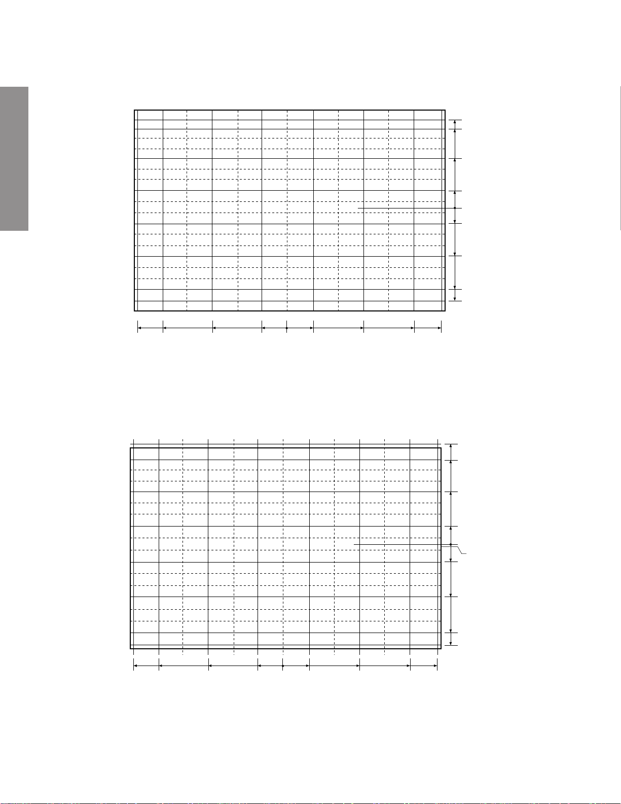
3 Screen adjustment dimensions
3-1 WIDE/4:3 (PAL mode)
GENERAL ADJUSTMENTSSPECIFIC INFORMATIONS
235
207.5
124.5
41.5
0
(screen center)
41.5
124.5
207.5
235
441
367.5
3-2 Super Wide (PAL mode)
220.5
73.5
0
73.5
220.5
367.5
441
249.0
220.0
130.5
40
0
(pattern center)
-5
49.5
136.5
441
367.5
220.5
0
73.5
Caution: Do not perform the VLIN adjustment.
– 28 –
73.5
220.5
367.5
221.0
249.0
441
Page 29
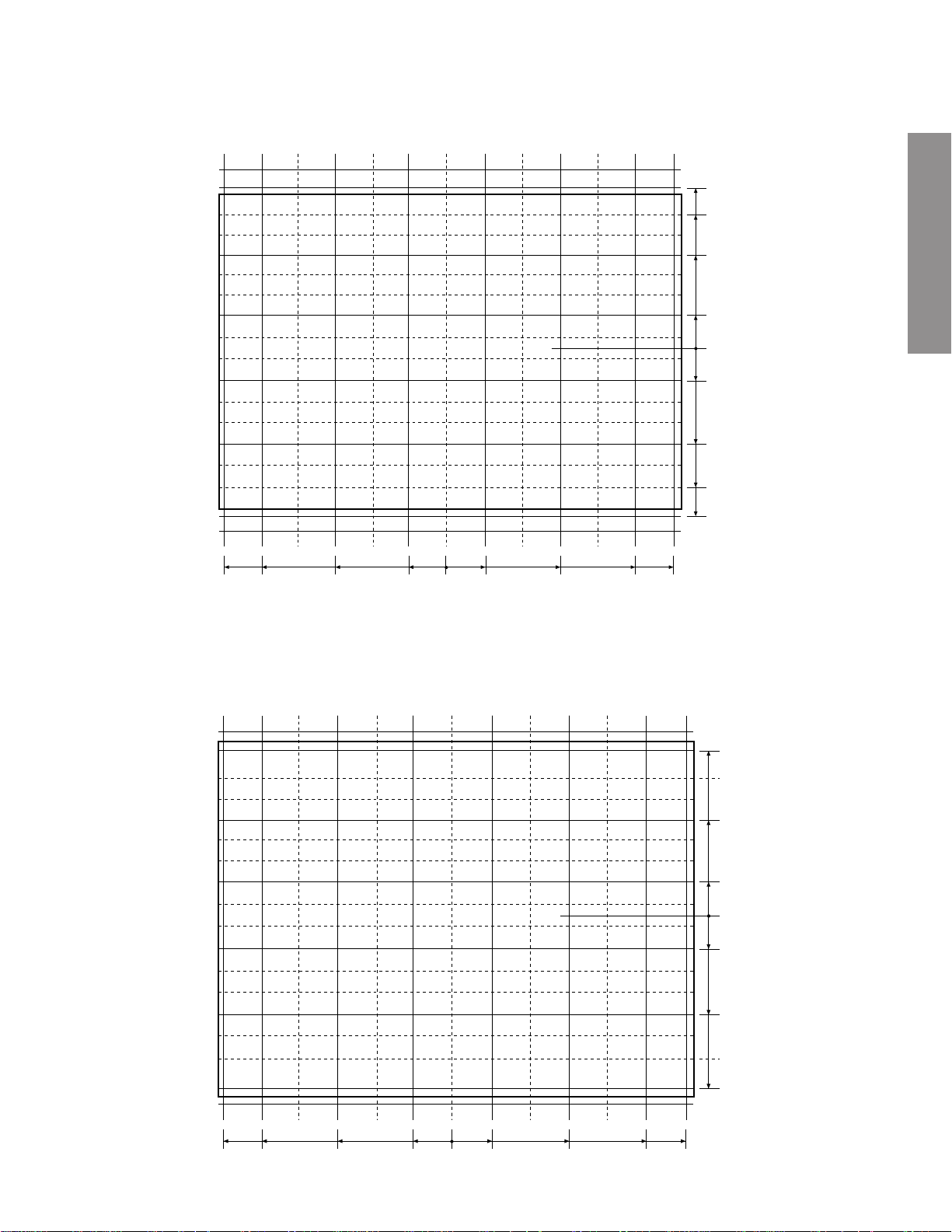
3-3 Cinema (PAL mode)
Note: The cursor will move outside the screen limits in the Cinema mode; theref ore, be careful to consider the position
of the cursor displayed on the screen when making adjustments.
262.5
227.5
157.5
52.5
0
52.5
157.5
227.5
262.5
GENERAL ADJUSTMENTSSPECIFIC INFORMATIONS
441
367.5
220.5
73.5
0
73.5
220.5
367.5
441
3-4 Subtitle (PAL mode)
Note: The cursor will move outside the screen limits in the Subtitle mode; theref ore, be careful to consider the position
of the cursor displayed on the screen when making adjustments.
Note: Please be aware that the Subtitle screen convergence pattern center is located at the center of the screen but the
image center is located approximately 13mm above that.
272
240
144
48
0
48
144
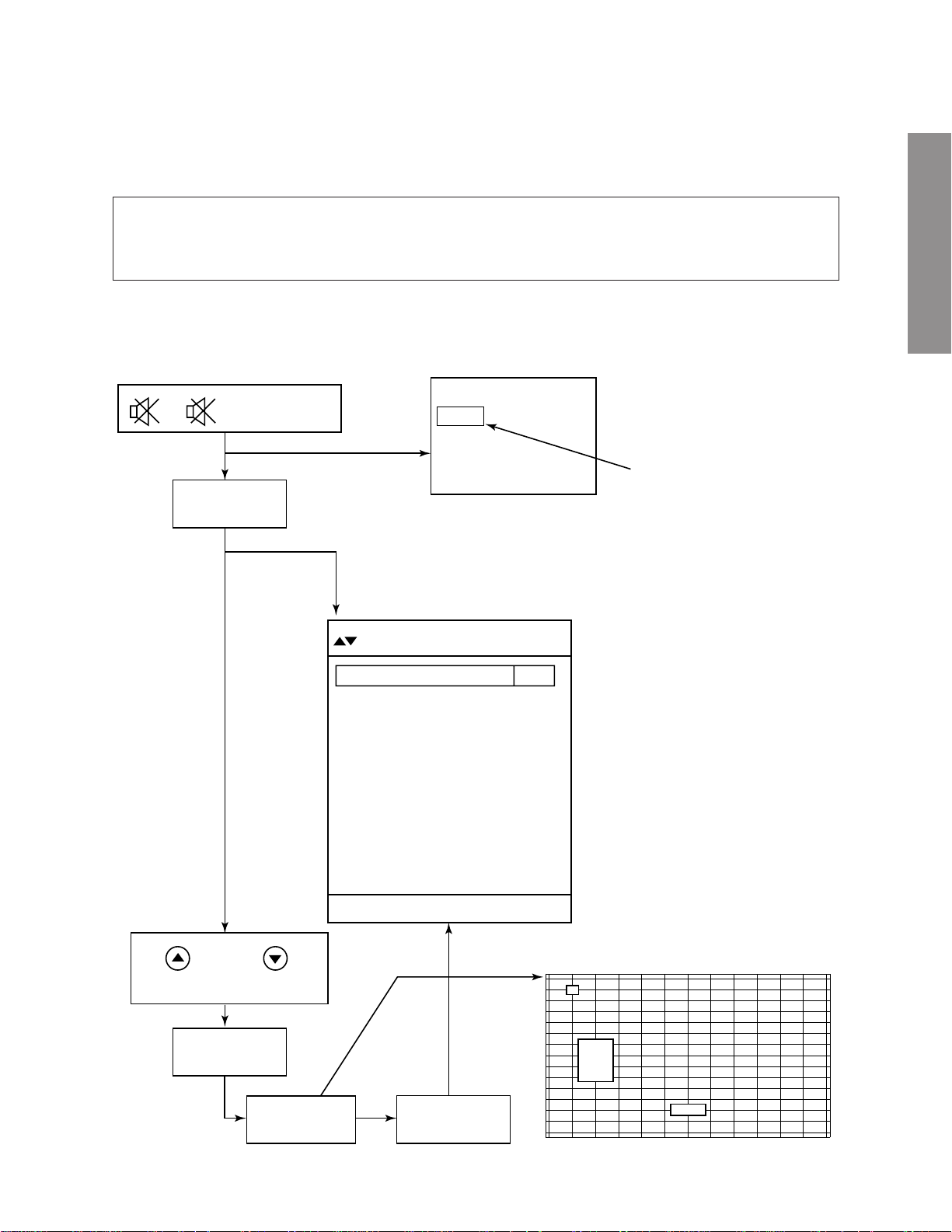
Screen limit changed
441
367.5
220.5
73.5
0
– 29 –
73.5
220.5
367.5
240
272
441
Page 30
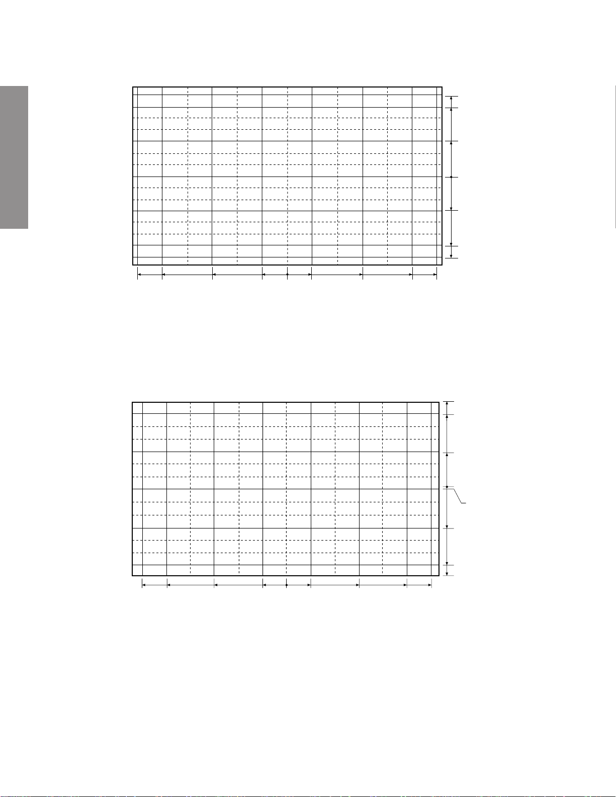
3-5 WIDE/4:3 (NTSC mode)
231
198
99
(screen center)
0
GENERAL ADJUSTMENTSSPECIFIC INFORMATIONS
3-6 Super Live (NTSC mode)
441
367.5
220.5
73.5
99
198
231
0
73.5
220.5
367.5
441
249
213
105
0
(pattern center)
-5
441
367.5
220.5
0
73.5
Caution: Do not perform the VLIN adjustment.
– 30 –
73.5
220.5
367.5
112
216
249
441
Page 31

3-7 Cinema (NTSC mode)
Note: The cursor will move outside the screen limits in the Cinema mode; therefore , be careful to consider the position
of the cursor displayed on the screen when making adjustments.
Note: Please be aware that the Cinema screen convergence pattern center is located at the center of the screen but
the image center is located approximately 13mm above that.
287
246
123
0
123
246
287
GENERAL ADJUSTMENTSSPECIFIC INFORMATIONS
441
367.5
220.5
73.5
0
73.5
220.5
367.5
441
3-8 Subtitle (NTSC mode)
Note: The cursor will move outside the screen limits in the Subtitle mode; therefore , be careful to consider the position
of the cursor displayed on the screen when making adjustments.
Note: Please be aware that the Subtitle screen convergence pattern center is located at the center of the screen but
the image center is located approximately 32mm above that.
266
228
114
0
114
228
266
441
367.5
220.5
73.5
0
73.5
220.5
367.5
441
– 31 –
Page 32

GENERAL ADJUSTMENTSSPECIFIC INFORMATIONS
CAUTION : Do not hold the optical system parts (lens and
mirror) with bare hand to avoid finger-prints on
the surface of those parts.
SCREEN AND MIRROR ALIGNMENTS
ASSEMBLING AND MOUNTING OF
FRONT SCREEN
* Please refer to MECHANICAL DISASSEMBLY page.38.
CLEANING OF LENS AND MIRROR
HOW TO CLEAN LENS AND MIRROR
1. Be sure to remove sand dust with an air brush, etc.
2. When it is stained slightly, breathe upon it and wipe away
with the specified cleaning cloth.
For other stains than the above, wipe the stains away with
the specified cloth into which a cleaning liquid has been
soaked.
Cleaning liquid ................... LENS LUSTER (Manufactured
by Edmund Scientific Co.), etc.
HOW TO CLEAN SCREEN
When cleaning the screen, use a soft cloth so as not to damage the screen.
1. Wipe the stain away with a diluted neutral detergent soaked
cloth.
2. Wipe the detergent away with a water soaked cloth.
3. Wipe the screen with a dry cloth to remove moisture on the
screen.
Note : Absolutely do not use alcohol, benzine, thinner, etc.
for cleaning in order not to wipe away the black print
on the surface.
– 32 –
Page 33

CIRCUIT CHECKS
HIGH VOLTAGE CHECK
CAUTION: There is no HIGH VOLTAGE ADJUSTMENT on this chassis. Checking should be done following the steps below.
1. Connect an accurate high voltage meter to the anode of the picture tube.
2. Turn on the receiver. Set the BRIGHTNESS and CONTRAST to minimum (zero beam current).
3. High voltage must be measured below (B) kV.
Refer to table-1 for high voltage (B).
(See SETTING & ADJUSTING DATA on page 34)
4. Vary the BRIGHTNESS to both extremes to be sure the high voltage does not exceed the limit under any conditions.
CAUTION:
When the following parts fail, check the High Voltage after replacing.
GENERAL ADJUSTMENTSSPECIFIC INFORMATIONS
Location
No.
T461
D489
Q480
Q483
R435
R489
R490
R450
C440
C443
C444
ANODE VOLTAGE MEASURING METHOD
CAUTION: Take extra precaution when measuring this high voltage. High voltages are also present in surrounding circuit
boards (CRT DRIVE assembly, DEFLECTION assembly, and POWER SUPPLY assembly).
1. Disconnect the FBT anode cable as outlined below. Measure high voltage at the point where the cable enters the FBT.
2. Holding the rubber cover firmly, turn it counterclockwise and check that the lock has been disengaged. (See Fig. b on page
8.)
3. Determine the extent of the rubber cover before disconnecting the cable.
4. Pull straight up the anode cable to disconnect.
5. When reconnecting the cable, proceed in the reverse order.
After reconnecting, tug on the cable to check that it is secure.
Name
Flyback Trans.
Zener Diode
Transistor
IC
Resistor
Resistor
Resistor
VR
Capacitor
Capacitor
Capacitor
Name
TFB3078BD
MTZJ3.6B
2SC2023
TA7508P(J)
33k ohm, ±5%
3.3k ohm, ±5%
3.3k ohm, ±5%
1k ohm
1000pF, ±3%
6800pF, ±3%
5100pF, ±3%
– 33 –
Page 34

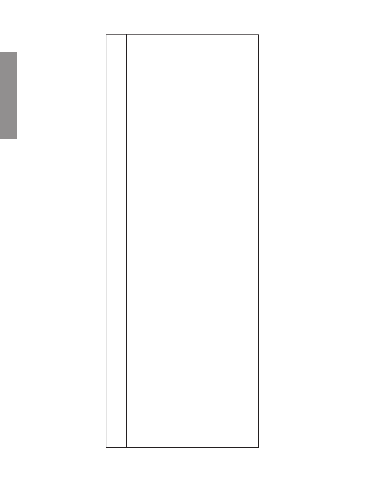
CHAPTER 2 SPECIFIC INFORMATIONS
SAFETY INSTRUCTIONS
GENERAL ADJUSTMENTSSPECIFIC INFORMATIONS
SERVICE MODE
ADJUSTING ITEMS AND DATAS IN THE SERVICE MODE:
SETTING & ADJUSTING DATA
40"
HIGH VOLTAGE AT ZERO BEAM: (A) 31.9 kV
MAX HIGH VOLTAGE:
AV VOLTAGE
Table-1
(B) 32.5 kV
(C) 230 V
Item
RCUT
GCUT
BCUT
RDRV
BDRV
CNTX
BRTC
COLC
TNTC
COLP
COLS
SCNT
BELL
SRY
SBY
R CUTOFF (B/W)
G CUTOFF (B/W)
B CUTOFF (B/W)
R DRIVE
B DRIVE
SUB CONTRAST MAX
SUB BRIGHT CEN
SUB COLOR CEN NTSC
SUB TINT CEN
SUB COLOR CEN PAL
SUB COLOR CEN SECAM
SUB CONTRAST
SECAM BELL FILTER
SECAM R-Y
SECAM B-Y
DESIGN MODE
ADJUSTING ITEMS AND DATAS IN THE DESIGN MODE:
Item Name of adjustment Preset Data 40PW03G 40PW03B Remarks
Adjustment
Reference data
40H
40H
40H
40H
40H
7FH
80H
FDH
45H
50H
38H
07H
80H
08H
08H
HPOS
VPOS
HIT
GMPS
VLIN
VSC
VPS
VCP
WID
PARA
CNR
TRAP
HCP
VFC
Table-2
Item
50Hz H-POSITION
V-POSITION
HEIGHT
V-POSITION (RASTER)
V-LINEARITY
V-S CORRECTION
V-SHIFT
V-COMPENSATION
PICTURE WIDTH
E-W PARABOLA
E-W CORNER
TRAPEZIUM
H-COMPENSATION
V-F CORRECTION
Adjustment
Reference data
0CH
01H
26H
00H
15H
26H
12H
05H
1EH
02H
10H
40H
04H
0FH
RCUT
OPT1
OPT0
OSD
○○○○○
RCUT
OPTION 1
OPTION 0
4CH
80H
Table-3
– 34 –
4CH 4CH
80H 81H
Page 35

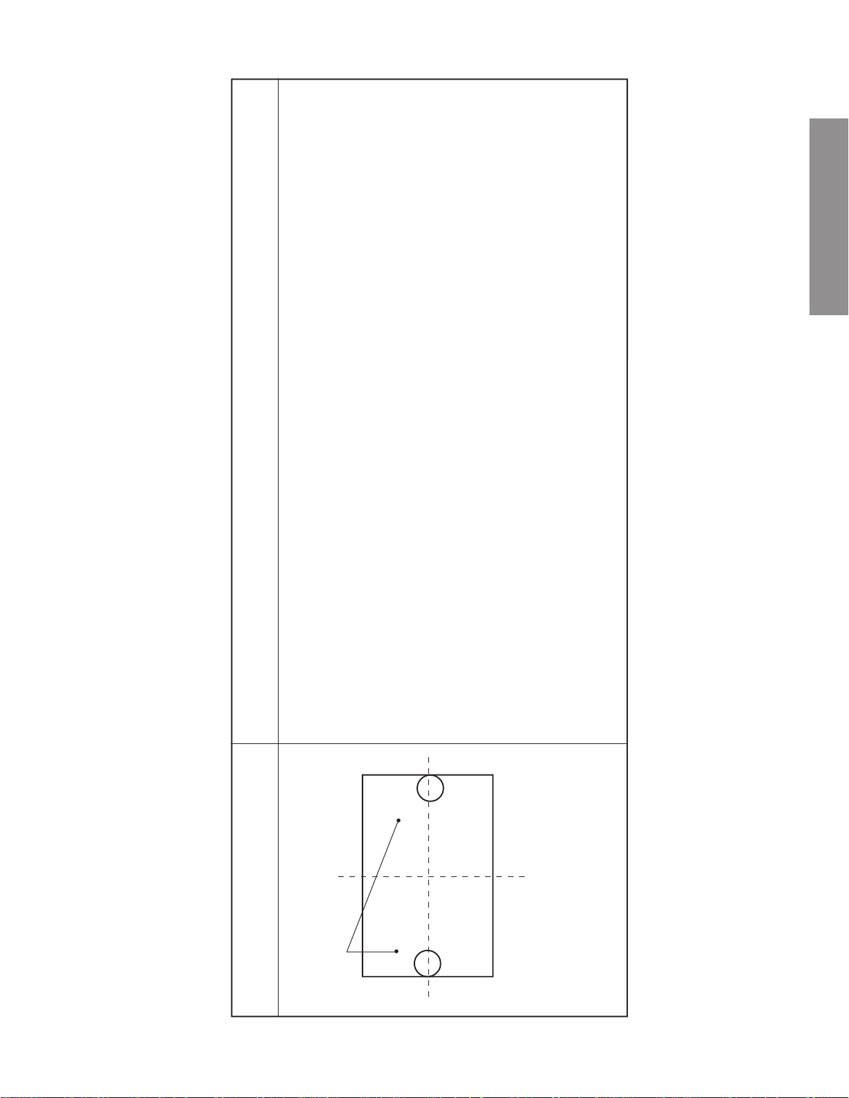
Front
LOCATION OF CONTROLS
GENERAL ADJUSTMENTSSPECIFIC INFORMATIONS
Back
HEAD PHONE
(VIDEO-3) S-VIDEO TERMINAL
VIDEO-3
MENU
VOLUME DOWN
VOLUME UP
POSITION DOWN
MAIN SWITCH
POWER (RED)
ON TIMER (GREEN)
BILINGUAL (ORANGE)
STEREO (GREEN)
EXIT
POSITION UP
WOOFER SWITCH
WOOFER OUT
VIDEO-1 (21PINS FULL)
VIDEO-2 (21PINS S-VIDEO/AV)
AERIAL TERMINAL
AUDIO OUT (FIXED)
VIDEO-3 (S-VIDEO/AUDIO)
VIDEO-3 (21PINS S-VIDEO/AUDIO)
– 35 –
Page 36

Remote Controller
GENERAL ADJUSTMENTSSPECIFIC INFORMATIONS
Keypad Number Buttons
1 or 2 Digit Channel Selection
Menu Control Buttons
Teletext
SIZE
MENU Buttons
3
9
a
^
f
Çi
CALL
TEXT
CH
yX
V
Power ON/ OFF
CALL
Teletext
•Programme Position up/down
VIDEO (+F)
F
F
1
2
4 5 6
7 8
-/--
0
?
v
SIZE
Picture Controls
ENTER
SELECT
Menu Control Buttons
ENTER
MENU EXIT
EXIT
•Stereo/Bilingual
REC
•Sound Mute
Video Recoder Buttons
to operate your Toshiba
Video Recorder
VTR/DVD
– 36 –
P
Volume
Page 37

MICRO
COMPUTER
MEMORY
QA01
Q801
I
2
CBUS
QA02
QV01
AV SW
R,G,B
TEXT
QZ01
Q501
R
G
B
QQ01 QQ02
Q601
CRT.R
CRT.G
CRT.B
MAIN/CENTER
Q901
Q911
Q921
Q301
Q404
Q751,Q752
QW51,QW52
DIGITAL
COM.
MAIN
AUDIO OUT
VIDEO OUT
VIDEO OUT
VIDEO OUT
SVM.OUT
V.OUT
H.OUT
CONVER
OUT
DIGITAL
CONVER
DPC.OUT
PROTECTOR
: I
2
C BLOCK
SW.REG.
E/W
CORRECTION
SECAM
1H
DELAY
COLOR/VIDEO/DEF
T862
Z801
+B
E1
21 PIN
(FULL)E221 PIN
(S+AV)
E3
21 PIN
(S+AV)
E3
S VIDEO
E3
FRONT
S+AV
AUDIO FIX
OUT
Y/V
L,R
OSD
QR01
QF01
R,G,B
V
L,R
L,R
QR01
RGB,
SW
L,R
V
V
Y
TIF
H001
MA
H002
GENERAL ADJUSTMENTSSPECIFIC INFORMATIONS
CIRCUIT BLOCK DIAGRAM
– 37 –
Page 38

K502
MECHANICAL DISASSEMBLY
K501
K503
GENERAL ADJUSTMENTSSPECIFIC INFORMATIONS
LABELS
16 SCREWS
8 SCREWS
A201
A264
10 SCREWS
8 SCREWS
A262
K601
A262
SCREWS
A420
A424
A103
A213 (A214)
(A223)
A212
A268
A102
6 SCREWS
K101
K102
K103
– 38 –
Page 39

CHASSIS AND CABINET REPLACEMENT PARTS LIST
WARNING: BEFORE SERVICING THIS CHASSIS, READ THE “X-RAY RADIATION PRECAUTION”, “SAFETY
PRECAUTION” AND “PRODUCT SAFETY NOTICE” ON PAGE 3 OF THIS MANUAL.
CAUTION: The international hazard symbols “ ” in the schematic diagram and the parts list designate com-
ponents which have special characteristics important for safety and should be replaced only with types identical to
those in the original circuit or specified in the parts list. The mounting position of replacements is to be identical
with originals. Before replacing any of these components, read carefully the PRODUCT SAFETY NOTICE . Do not
degrade the safety of the receiver through improper servicing.
NOTICE:
•
The part number must be used when ordering parts, in order to assist in processing, be sure to include the Model
number and Description.
•
The PC board assembly with * mark is no longer available after the end of the production.
ABBREVIATIONS:
Capacitors ............. CD : Ceramic Disk PF : Plastic Film EL : Electrolytic
Resistors ............... CF : Carbon Film CC : Carbon Composition MF : Metal Film
OMF : Oxide Metal Film VR : Variable Resistor FR : Fusible Resistor
(All CD and PF capacitors are ±5%, 50V and all resistors, ±5%, 1/6W unless otherwise noted.)
Models : 40PW03G, 40PW03B
Location
No.
Part No. Description
Location
No.
Part No. Description
GENERAL ADJUSTMENTSSPECIFIC INFORMATIONS
CAPACITORSCAPACITORS
CAPACITORS
CAPACITORSCAPACITORS
C101 24793220 EL, 22?F, ±20%, 10V
C102 24762221 EL, 220?F, ±20%, 10V
C105 24212102 CD, 1000pF, ±10%
C106 24797100 EL, 10?F, ±20%, 50V
C115 24232103 CD, 0.01?F, +80%, -20%
C116 24762221 EL, 220?F, ±20%, 10V
C150 24763102 EL, 1000?F, ±20%, 16V
C183 24766479 EL, 4.7?F, ±20%, 50V
C194 24232103 CD, 0.01?F, +80%, -20%
C201 24538104 PF, 0.1?F
C202 24814103 Chip, 0.01?F, +80%, -20%
C203 24538104 PF, 0.1?F
C204 24669010 EL, 1?F, ±20%, 50V
C205 24669229 EL, 2.2?F, ±20%, 50V
C206 24206220 EL, 22?F, ±20%, 50V
C212 24794100 EL, 10?F, ±20%, 16V
C214 24591334 PF, 0.33?F
C219 24781100 Chip, 10pF, ±0.5pF%, SL
C220 24781100 Chip, 10pF, ±0.5pF%, SL
C221 24781100 Chip, 10pF, ±0.5pF%, SL
C228 24814103 Chip, 0.01?F, +80%, -20%
C229 24669010 EL, 1?F, ±20%, 50V
C230 24763221 EL, 220?F, ±20%, 16V
C231 24814103 Chip, 0.01?F, +80%, -20%
C232 24669010 EL, 1?F, ±20%, 50V
C260 24085967 EL, 47?F, ±20%, 16V,
C261 24669101 EL, 100?F, ±20%, 50V
C262 24814103 Chip, 0.01?F, +80%, -20%
C264 24781150 Chip, 15pF, SL
C273 24206229 EL, 2.2?F, ±20%, 50V
C281 24763101 EL, 100?F, ±20%, 16V
C282 24232103 CD, 0.01?F, +80%, -20%
C283 24794100 EL, 10?F, ±20%, 16V
C284 24794100 EL, 10?F, ±20%, 16V
C295 24232103 CD, 0.01?F, +80%, -20%
C303 24214471 CD, 470pF, ±10%, 500V
C305 24617912 EL, 2.2?F, ±10%, 50V
C306 24617858 EL, 3300?F, ±20%, 35V
C307 24082270 PF, 0.033?F, 100V
Non-Polar
C308 24669221 EL, 220?F, ±20%, 50V
C309 24212101 CD, 100pF, ±10%
C310 24669222 EL, 2200?F, ±20%, 50V
C311 24214561 CD, 560pF, ±10%, 500V
C313 24082057 PF, 0.22?F, 100V
C314 24591103 PF, 0.01?F
C315 24797229 EL, 2.2?F, ±20%, 50V
C316 24232103 CD, 0.01?F, +80%, -20%
C318 24666222 EL, 2200?F, ±20%, 16V
C319 24591102 PF, 1000pF
C320 24669101 EL, 100?F, ±20%, 50V
C321 24591183 PF, 0.018?F
C322 24617915 EL, 1?F, ±10%, 50V
C323 24567474 PF, 0.47?F
C324 24567684 PF, 0.68?F
C330 24591104 PF, 0.1?F
C331 24669229 EL, 2.2?F, ±20%, 50V
C344 24591103 PF, 0.01?F
C351 24667222 EL, 2200?F, ±20%, 25V
C355 24669010 EL, 1?F, ±20%, 50V
C357 24669100 EL, 10?F, ±20%, 50V
C360 24667100 EL, 10?F, ±20%, 25V
C361 24669100 EL, 10?F, ±20%, 50V
C362 24591104 PF, 0.1?F
C363 24085942 EL, 10?F, ±20%, 16V,
Non-Polar
C364 24666100 EL, 10?F, ±20%, 16V
C370 24669101 EL, 100?F, ±20%, 50V
C371 24669100 EL, 10?F, ±20%, 50V
C372 24591104 PF, 0.1?F
C388 24591334 PF, 0.33?F
C403 24591223 PF, 0.022?F
C403 24828124 PF, 0.12?F, 200V
C404 24797229 EL, 2.2?F, ±20%, 50V
C413 24214821 CD, 820pF, ±10%, 500V
C415 24815392 Chip, 3900pF, ±10%
C416 24678100 EL, 10?F, ±20%, 200V
C417 24214391 CD, 390pF, ±10%, 500V
C418 24095883 PF, 0.015?F, ±3%, 630V
C419 24095803 PF, 0.062?F, 400V
C420 24666101 EL, 100?F, ±20%, 16V
– 39 –
Page 40

Location
No.
Part No. Description
Location
No.
Part No. Description
C423 24095779 PF, 0.062?F, 400V
C430 24814103 Chip, 0.01?F, +80%, -20%
C431 24763102 EL, 1000?F, ±20%, 16V
C440 24082326 PF, 1300pF, ±3%, 1500V
C443 24082348 PF, 6800pF, ±3%, 1500V
C444 24082287 PF, 5100pF, ±3%, 1800V
C445 24828473 PF, 0.047?F, 200V
C446 24679330 EL, 33?F, ±20%, 250V
C447 24667102 EL, 1000?F, ±20%, 25V
C448 24640908 EL, 33?F, ±20%, 160V
C460 24669331 EL, 330?F, ±20%, 50V
C463 24212152 CD, 1500pF, ±10%
GENERAL ADJUSTMENTSSPECIFIC INFORMATIONS
C464 24640872 EL, 10?F, ±20%, 100V
C465 24591332 PF, 3300pF
C466 24567394 PF, 0.39?F
C467 24820153 PF, 0.015?F, 630V
C468 24567474 PF, 0.47?F
C471 24206479 EL, 4.7?F, ±20%, 50V
C475 24820103 PF, 0.01?F, 630V
C477 24092347 CD, 1500pF, ±10%, 2kV
C481 24567104 PF, 0.1?F
C482 24591152 PF, 1500pF
C483 24567224 PF, 0.22?F
C484 24567104 PF, 0.1?F
C485 24669101 EL, 100?F, ±20%, 50V
C493 24591124 PF, 0.12?F
C501 24781101 Chip, 100pF, SL
C502 24814103 Chip, 0.01?F, +80%, -20%
C503 24763221 EL, 220?F, ±20%, 16V
C504 24591222 PF, 2200pF
C505 24774120 Chip, 12pF, CH
C507 24774120 Chip, 12pF, CH
C508 24669010 EL, 1?F, ±20%, 50V
C509 24763101 EL, 100?F, ±20%, 16V
C510 24763101 EL, 100?F, ±20%, 16V
C511 24814103 Chip, 0.01?F, +80%, -20%
C512 24206228 EL, 0.22?F, ±20%, 50V
C513 24814103 Chip, 0.01?F, +80%, -20%
C514 24538104 PF, 0.1?F
C515 24538104 PF, 0.1?F
C516 24781102 Chip, 1000pF, SL
C517 24774010 Chip, 1pF, ±0.25pF, CH
C519 24774010 Chip, 1pF, ±0.25pF, CH
C520 24781102 Chip, 1000pF, SL
C521 24781102 Chip, 1000pF, SL
C524 24781122 Chip, 1200pF, SL
C525 24774181 Chip, 180pF, CH
C554 24814103 Chip, 0.01?F, +80%, -20%
C555 24669010 EL, 1?F, ±20%, 50V
C556 24669010 EL, 1?F, ±20%, 50V
C601 24590102 PF, 1000pF
C602 24590102 PF, 1000pF
C603 24669100 EL, 10?F, ±20%, 50V
C604 24669100 EL, 10?F, ±20%, 50V
C605 24667101 EL, 100?F, ±20%, 25V
C606 24667101 EL, 100?F, ±20%, 25V
C607 24538104 PF, 0.1?F(40PW03G)
C607 24567104 PF, 0.1?F(40PW03B)
C608 24538104 PF, 0.1?F(40PW03G)
C608 24567104 PF, 0.1?F(40PW03B)
C609 24669102 EL, 1000?F, ±20%, 50V
C610 24669102 EL, 1000?F, ±20%, 50V
C611 24667221 EL, 220?F, ±20%, 25V
C613 24666471 EL, 470?F, ±20%, 16V
C636 24666100 EL, 10?F, ±20%, 16V
C661 24436101 CD, 100pF
C665 24669229 EL, 2.2?F, ±20%, 50V
C666 24669229 EL, 2.2?F, ±20%, 50V
C671 24669100 EL, 10?F, ±20%, 50V
C672 24232103 CD, 0.01?F, +80%, -20%
C673 24781102 Chip, 1000pF, SL
C674 24669100 EL, 10?F, ±20%, 50V
C674 24781102 Chip, 1000pF, SL
C675 24669100 EL, 10?F, ±20%, 50V
C675 24781102 Chip, 1000pF, SL
C676 24669100 EL, 10?F, ±20%, 50V
C676 24781102 Chip, 1000pF, SL
C677 24668221 EL, 220?F, ±20%, 35V
C678 24781102 Chip, 1000pF, SL
C679 24781102 Chip, 1000pF, SL
C680 24669222 EL, 2200?F, ±20%, 50V
C681 24781102 Chip, 1000pF, SL
C682 24669010 EL, 1?F, ±20%, 50V
C682 24781102 Chip, 1000pF, SL
C696 24762102 EL, 1000?F, ±20%, 10V
C701 24781330 Chip, 33pF, SL
C702 24781330 Chip, 33pF, SL
C711 24206100 EL, 10?F, ±20%, 50V
C714 24092293 Chip, 0.1?F, +80%, -20%, 25V
C715 24092441 Chip, 1?F, +80%, -20%, 16V
C716 24815822 Chip, 0.0082?F, ±10%
C717 24774470 Chip, 47pF, CH
C718 24774470 Chip, 47pF, CH
C719 24794101 EL, 100?F, ±20%, 16V
C720 24092293 Chip, 0.1?F, +80%, -20%, 25V
C721 24567104 PF, 0.1?F
C722 24092293 Chip, 0.1?F, +80%, -20%, 25V
C724 24092293 Chip, 0.1?F, +80%, -20%, 25V
C725 24092293 Chip, 0.1?F, +80%, -20%, 25V
C726 24092293 Chip, 0.1?F, +80%, -20%, 25V
C727 24092293 Chip, 0.1?F, +80%, -20%, 25V
C728 24763221 EL, 220?F, ±20%, 16V
C729 24092293 Chip, 0.1?F, +80%, -20%, 25V
C730 24567104 PF, 0.1?F
C731 24766010 EL, 1?F, ±20%, 50V
C732 24590822 PF, 0.0082?F
C735 24092293 Chip, 0.1?F, +80%, -20%, 25V
C736 24794470 EL, 47?F, ±20%, 16V
C739 24092293 Chip, 0.1?F, +80%, -20%, 25V
C740 24092293 Chip, 0.1?F, +80%, -20%, 25V
C741 24794470 EL, 47?F, ±20%, 16V
C742 24794470 EL, 47?F, ±20%, 16V
C743 24092293 Chip, 0.1?F, +80%, -20%, 25V
C744 24092293 Chip, 0.1?F, +80%, -20%, 25V
C745 24794470 EL, 47?F, ±20%, 16V
C746 24794470 EL, 47?F, ±20%, 16V
C747 24092293 Chip, 0.1?F, +80%, -20%, 25V
C748 24092293 Chip, 0.1?F, +80%, -20%, 25V
C749 24794470 EL, 47?F, ±20%, 16V
C750 24794470 EL, 47?F, ±20%, 16V
C756 24781391 Chip, 390pF, SL
C761 24590182 PF, 1800pF
C762 24590562 PF, 5600pF
C763 24774391 Chip, 390pF, CH
C765 24590182 PF, 1800pF
C766 24590562 PF, 5600pF
C767 24774391 Chip, 390pF, CH
C769 24590182 PF, 1800pF
– 40 –
Page 41

Location
No.
Part No. Description
Location
No.
Part No. Description
C770 24590562 PF, 5600pF
C771 24774391 Chip, 390pF, CH
C773 24590182 PF, 1800pF
C774 24590562 PF, 5600pF
C775 24774391 Chip, 390pF, CH
C777 24590182 PF, 1800pF
C778 24590562 PF, 5600pF
C779 24774391 Chip, 390pF, CH
C781 24590182 PF, 1800pF
C782 24590562 PF, 5600pF
C783 24774391 Chip, 390pF, CH
C795 24761221 EL, 220?F, ±20%, 6.3V
C798 24763101 EL, 100?F, ±20%, 16V
C799 24763101 EL, 100?F, ±20%, 16V
* C801 24082374 PF, 0.22?F, ±20%, AC250V
* C802 24092557 CD, 220pF, ±20%, AC250V
* C803 24092557 CD, 220pF, ±20%, AC250V
* C804 24092570 CD, 3300pF, ±20%, AC250V
* C805 24082374 PF, 0.22?F, ±20%, AC250V
C807 24073058 EL, 2200?F, ±20%, 25V
C808 24617787 EL, 470?F, ±20%, 16V
C809 24567105 PF, 1?F
C810 24086935 EL, 560?F, ±20%, 400V
C811 24676478 EL, 0.47?F, ±20%, 100V
C812 24092281 CD, 4700pF, ±20%, AC250V
C813 24092281 CD, 4700pF, ±20%, AC250V
C814 24678229 EL, 2.2?F, ±20%, 200V
C815 24567474 PF, 0.47?F
C816 24617817 EL, 22?F, ±20%, 50V
C817 24567224 PF, 0.22?F
C819 24214102 CD, 1000pF, ±10%, 500V
C820 24567224 PF, 0.22?F
C821 24092480 CD, 680pF, ±10%, 2kV
C822 24092481 CD, 820pF, ±10%, 2kV
C823 24092478 CD, 470pF, ±10%, 2kV
C824 24214103 CD, 0.01?F, ±10%, 500V
C825 24591472 PF, 4700pF
C826 24092474 CD, 220pF, ±10%, 2kV
C828 24820683 PF, 0.068?F, 630V
C829 24617820 EL, 100?F, ±20%, 50V
C830 24567105 PF, 1?F
C831 24669220 EL, 22?F, ±20%, 50V
C853 24668102 EL, 1000?F, ±20%, 35V
C855 24214471 CD, 470pF, ±10%, 500V
C856 24214471 CD, 470pF, ±10%, 500V
C857 24214471 CD, 470pF, ±10%, 500V
C858 24214471 CD, 470pF, ±10%, 500V
C859 24214471 CD, 470pF, ±10%, 500V
C860 24669471 EL, 470?F, ±20%, 50V
C861 24668332 EL, 3300?F, ±20%, 35V
C862 24668471 EL, 470?F, ±20%, 35V
C863 24668332 EL, 3300?F, ±20%, 35V
C864 24668471 EL, 470?F, ±20%, 35V
C865 24214471 CD, 470pF, ±10%, 500V
C866 24214471 CD, 470pF, ±10%, 500V
C867 24214471 CD, 470pF, ±10%, 500V
C868 24214471 CD, 470pF, ±10%, 500V
C869 24669222 EL, 2200?F, ±20%, 50V
C870 24214471 CD, 470pF, ±10%, 500V
C871 24214471 CD, 470pF, ±10%, 500V
C872 24214471 CD, 470pF, ±10%, 500V
C873 24214471 CD, 470pF, ±10%, 500V
C874 24212102 CD, 1000pF, ±10%
C875 24667472 EL, 4700?F, ±20%, 25V
C876 24086916 EL, 330?F, ±20%, 160V
C877 24092475 CD, 220pF, ±10%, 2kV
C878 24092475 CD, 220pF, ±10%, 2kV
C879 24092475 CD, 220pF, ±10%, 2kV
C880 24092475 CD, 220pF, ±10%, 2kV
C881 24567474 PF, 0.47?F
C882 24617817 EL, 22?F, ±20%, 50V
C883 24082229 PF, 0.1?F, ±10%, 250V
C884 24617816 EL, 10?F, ±20%, 50V
C885 24617813 EL, 2.2?F, ±20%, 50V
C886 24677470 EL, 47?F, ±20%, 160V
C889 24669010 EL, 1?F, ±20%, 50V
C891 24669010 EL, 1?F, ±20%, 50V
C901 24211102 CD, 1000pF, ±10%, 2kV
C902 24794100 EL, 10?F, ±20%, 16V
C903 24232103 CD, 0.01?F, +80%, -20%
C904 24436391 CD, 390pF
C905 24214102 CD, 1000pF, ±10%, 500V
C911 24211102 CD, 1000pF, ±10%, 2kV
C912 24794100 EL, 10?F, ±20%, 16V
C913 24232103 CD, 0.01?F, +80%, -20%
C914 24436561 CD, 560pF
C915 24679330 EL, 33?F, ±20%, 250V
C915A 23960136 Adhesive, TSE3843-W
C916 24794101 EL, 100?F, ±20%, 16V
C921 24211102 CD, 1000pF, ±10%, 2kV
C922 24794100 EL, 10?F, ±20%, 16V
C924 24232103 CD, 0.01?F, +80%, -20%
C926 24436471 CD, 470pF
C941 24797478 EL, 0.47?F, ±20%, 50V
C943 24667102 EL, 1000?F, ±20%, 25V
C944 24206100 EL, 10?F, ±20%, 50V
C961 24666101 EL, 100?F, ±20%, 16V
C962 24203100 EL, 10?F, ±20%, 16V
C963 24232103 CD, 0.01?F, +80%, -20%
C964 24591104 PF, 0.1?F
C6101 24232103 CD, 0.01?F, +80%, -20%
C6102 24232103 CD, 0.01?F, +80%, -20%
C7701 24761221 EL, 220?F, ±20%, 6.3V
C7703 24232103 CD, 0.01?F, +80%, -20%
C7721 24212102 CD, 1000pF, ±10%
C7722 24436101 CD, 100pF
C7724 24667101 EL, 100?F, ±20%, 25V
C7725 24667101 EL, 100?F, ±20%, 25V
C7726 24212102 CD, 1000pF, ±10%
C7727 24436101 CD, 100pF
C7729 24212102 CD, 1000pF, ±10%
C7730 24436101 CD, 100pF
C7732 24212102 CD, 1000pF, ±10%
C7733 24436101 CD, 100pF
C7735 24667101 EL, 100?F, ±20%, 25V
C7736 24669101 EL, 100?F, ±20%, 50V
C7737 24212102 CD, 1000pF, ±10%
C7738 24436101 CD, 100pF
C7740 24212102 CD, 1000pF, ±10%
C7741 24436101 CD, 100pF
C7742 24436330 CD, 33pF
C7743 24436330 CD, 33pF
C7747 24667101 EL, 100?F, ±20%, 25V
C7748 24567104 PF, 0.1?F
C7749 24567104 PF, 0.1?F
C7750 24667101 EL, 100?F, ±20%, 25V
C7751 24667101 EL, 100?F, ±20%, 25V
C7752 24567104 PF, 0.1?F
GENERAL ADJUSTMENTSSPECIFIC INFORMATIONS
– 41 –
Page 42

Location
No.
Part No. Description
Location
No.
Part No. Description
C7753 24567104 PF, 0.1?F
C7754 24667101 EL, 100?F, ±20%, 25V
C7755 24667101 EL, 100?F, ±20%, 25V
C7756 24567104 PF, 0.1?F
C7757 24567104 PF, 0.1?F
C7758 24667101 EL, 100?F, ±20%, 25V
C7760 24667470 EL, 47?F, ±20%, 25V
C7761 24667470 EL, 47?F, ±20%, 25V
C7762 24669100 EL, 10?F, ±20%, 50V
C7763 24667470 EL, 47?F, ±20%, 25V
C7764 24598331 PF, 330pF
C7767 24667470 EL, 47?F, ±20%, 25V
GENERAL ADJUSTMENTSSPECIFIC INFORMATIONS
C7768 24567104 PF, 0.1?F
C7769 24232103 CD, 0.01?F, +80%, -20%
C7770 24669470 EL, 47?F, ±20%, 50V
C7771 24567103 PF, 0.01?F
C7772 24667101 EL, 100?F, ±20%, 25V
C7773 24669101 EL, 100?F, ±20%, 50V
C7774 24436331 CD, 330pF
C7775 24667101 EL, 100?F, ±20%, 25V
C7776 24667470 EL, 47?F, ±20%, 25V
C7777 24669470 EL, 47?F, ±20%, 50V
C7778 24567104 PF, 0.1?F
C7779 24669479 EL, 4.7?F, ±20%, 50V
C7780 24591102 PF, 1000pF
C8301 24666101 EL, 100?F, ±20%, 16V
C8303 24669100 EL, 10?F, ±20%, 50V
C8304 24666101 EL, 100?F, ±20%, 16V
C8306 24666470 EL, 47?F, ±20%, 16V
C8307 24591334 PF, 0.33?F
C9602 24794100 EL, 10?F, ±20%, 16V
CA14 24232103 CD, 0.01?F, +80%, -20%
CA15 24232103 CD, 0.01?F, +80%, -20%
CA19 24436101 CD, 100pF
CA24 24436101 CD, 100pF
CA41 24436101 CD, 100pF
CA42 24436101 CD, 100pF
CA43 24436101 CD, 100pF
CA68 24794100 EL, 10?F, ±20%, 16V
CA69 24232103 CD, 0.01?F, +80%, -20%
CA106 24436101 CD, 100pF
CA107 24538104 PF, 0.1?F(40PW03G)
CA107 24567104 PF, 0.1?F(40PW03B)
CA108 24538103 PF, 0.01?F(40PW03G)
CA108 24590103 PF, 0.01?F(40PW03B)
CA109 24538103 PF, 0.01?F(40PW03G)
CA109 24590103 PF, 0.01?F(40PW03B)
CA420 24794100 EL, 10?F, ±20%, 16V
CA430 24232103 CD, 0.01?F, +80%, -20%
CA440 24232103 CD, 0.01?F, +80%, -20%
CB01 24794470 EL, 47?F, ±20%, 16V
CB90 24232103 CD, 0.01?F, +80%, -20%
CC08 24815102 Chip, 0.001?F, ±10%
CC10 24781820 Chip, 82pF, SL
CC15 24212102 CD, 1000pF, ±10%
CC23 24814103 Chip, 0.01?F, +80%, -20%
CC28 24232103 CD, 0.01?F, +80%, -20%
CC29 24232103 CD, 0.01?F, +80%, -20%
CC30 24567474 PF, 0.47?F
CC39 24232103 CD, 0.01?F, +80%, -20%
CC40 24781470 Chip, 47pF, SL
CC41 24781470 Chip, 47pF, SL
CC42 24781470 Chip, 47pF, SL
CC45 24774050 CD, 5pF, ±0.25pF, CH
CC46 24774050 CD, 5pF, ±0.25pF, CH
CC47 24232103 CD, 0.01?F, +80%, -20%
CC48 24232103 CD, 0.01?F, +80%, -20%
CF03 24567104 PF, 0.1?F
CF04 24766101 EL, 100?F, ±20%, 50V
CF05 24766101 EL, 100?F, ±20%, 50V
CF06 24774220 Chip, 22pF, CH
CF07 24774220 Chip, 22pF, CH
CF08 24567104 PF, 0.1?F
CF09 24567104 PF, 0.1?F
CF10 24206100 EL, 10?F, ±20%, 50V
CF11 24567104 PF, 0.1?F
CF12 24814103 Chip, 0.01?F, +80%, -20%
CF14 24814103 Chip, 0.01?F, +80%, -20%
CF16 24567224 PF, 0.22?F
CF18 24794101 EL, 100?F, ±20%, 16V
CF19 24814103 Chip, 0.01?F, +80%, -20%
CF20 24766010 EL, 1?F, ±20%, 50V
CQ01 24781102 Chip, 1000pF, SL
CQ02 24781820 Chip, 82pF, SL
CQ03 24781102 Chip, 1000pF, SL
CQ04 24203100 EL, 10?F, ±20%, 16V
CQ05 24591563 PF, 0.056?F
CQ07 24591203 PF, 0.02?F
CQ08 24567683 PF, 0.068?F
CQ09 24206229 EL, 2.2?F, ±20%, 50V
CQ10 24591223 PF, 0.022?F
CQ11 24206229 EL, 2.2?F, ±20%, 50V
CQ12 24781820 Chip, 82pF, SL
CQ13 24669010 EL, 1?F, ±20%, 50V
CQ14 24669010 EL, 1?F, ±20%, 50V
CQ15 24763101 EL, 100?F, ±20%, 16V
CQ16 24814103 Chip, 0.01?F, +80%, -20%
CQ17 24774150 Chip, 15pF, CH
CQ18 24781820 Chip, 82pF, SL
CQ19 24590103 PF, 0.01?F
CQ20 24567104 PF, 0.1?F
CQ21 24794470 EL, 47?F, ±20%, 16V
CQ22 24814103 Chip, 0.01?F, +80%, -20%
CQ23 24567104 PF, 0.1?F
CQ24 24567104 PF, 0.1?F
CQ25 24797100 EL, 10?F, ±20%, 50V
CQ26 24567104 PF, 0.1?F
CQ27 24567104 PF, 0.1?F
CQ28 24797478 EL, 0.47?F, ±20%, 50V
CQ29 24794101 EL, 100?F, ±20%, 16V
CQ30 24814103 Chip, 0.01?F, +80%, -20%
CQ31 24797478 EL, 0.47?F, ±20%, 50V
CQ32 24590103 PF, 0.01?F
CQ33 24567104 PF, 0.1?F
CQ34 24567104 PF, 0.1?F
CQ35 24206478 EL, 0.47?F, ±20%, 50V
CQ36 24206478 EL, 0.47?F, ±20%, 50V
CQ37 24669010 EL, 1?F, ±20%, 50V
CQ38 24669010 EL, 1?F, ±20%, 50V
CQ39 24669010 EL, 1?F, ±20%, 50V
CQ40 24781820 Chip, 82pF, SL
CQ41 24781090 Chip, 9pF, ±0.5pF, SL
CQ42 24781090 Chip, 9pF, ±0.5pF, SL
CQ43 24781090 Chip, 9pF, ±0.5pF, SL
CQ45 24781102 Chip, 1000pF, SL
CQ46 24781102 Chip, 1000pF, SL
CQ61 24781102 Chip, 1000pF, SL
CQ62 24781470 Chip, 47pF, SL
– 42 –
Page 43

Location
No.
Part No. Description
Location
No.
Part No. Description
CQ63 24781470 Chip, 47pF, SL
CR01 24206010 EL, 1?F, ±20%, 50V
CR01 24567104 PF, 0.1?F
CR02 24232103 CD, 0.01?F, +80%, -20%
CR02 24567104 PF, 0.1?F
CR03 24436101 CD, 100pF
CR03 24567104 PF, 0.1?F
CR04 24567104 PF, 0.1?F
CR05 24567104 PF, 0.1?F
CR06 24567104 PF, 0.1?F
CR07 24814103 Chip, 0.01?F, +80%, -20%
CR08 24794100 EL, 10?F, ±20%, 16V
CR09 24538104 PF, 0.1?F(40PW03G)
CR09 24567104 PF, 0.1?F
CR09 24814103 Chip, 0.01?F, +80%, -20%
CR10 24794470 EL, 47?F, ±20%, 16V
CR11 24538104 PF, 0.1?F(40PW03G)
CR11 24567104 PF, 0.1?F(40PW03B)
CR12 24567104 PF, 0.1?F
CR13 24567104 PF, 0.1?F
CR14 24567104 PF, 0.1?F
CR18 24538104 PF, 0.1?F(40PW03G)
CR18 24567104 PF, 0.1?F(40PW03B)
CR19 24538104 PF, 0.1?F(40PW03G)
CR19 24567104 PF, 0.1?F(40PW03B)
CR20 24538104 PF, 0.1?F(40PW03G)
CR20 24567104 PF, 0.1?F(40PW03B)
CS01 24085944 EL, 2.2?F, ±20%, 50V,
Non-Polar
CS02 24085944 EL, 2.2?F, ±20%, 50V,
Non-Polar
CS03 24206229 EL, 2.2?F, ±20%, 50V
CS04 24206229 EL, 2.2?F, ±20%, 50V
CS05 24206229 EL, 2.2?F, ±20%, 50V
CS06 24206229 EL, 2.2?F, ±20%, 50V
CS07 24206229 EL, 2.2?F, ±20%, 50V
CS08 24206229 EL, 2.2?F, ±20%, 50V
CS12 24781102 Chip, 1000pF, SL
CS13 24781102 Chip, 1000pF, SL
CS14 24206100 EL, 10?F, ±20%, 50V
CS15 24206100 EL, 10?F, ±20%, 50V
CS17 24203100 EL, 10?F, ±20%, 16V
CS18 24203100 EL, 10?F, ±20%, 16V
CS19 24206478 EL, 0.47?F, ±20%, 50V
CS22 24203100 EL, 10?F, ±20%, 16V
CS23 24203100 EL, 10?F, ±20%, 16V
CS53 24781102 Chip, 1000pF, SL
CV01 24567103 PF, 0.01?F
CV02 24085970 EL, 10?F, ±20%, 16V,
Non-Polar
CV03 24203100 EL, 10?F, ±20%, 16V
CV04 24203100 EL, 10?F, ±20%, 16V
CV05 24814103 Chip, 0.01?F, +80%, -20%
CV06 24203100 EL, 10?F, ±20%, 16V
CV08 24763102 EL, 1000?F, ±20%, 16V
CV10 24085970 EL, 10?F, ±20%, 16V,
Non-Polar
CV11 24781331 Chip, 330pF, SL
CV12 24092178 Chip, 0.1?F, ±10%, 25V
CV13 24814103 Chip, 0.01?F, +80%, -20%
CV14 24781102 Chip, 1000pF, SL
CV15 24781102 Chip, 1000pF, SL
CV16 24781102 Chip, 1000pF, SL
CV17 24781102 Chip, 1000pF, SL
CV18 24781102 Chip, 1000pF, SL
CV19 24781102 Chip, 1000pF, SL
CV20 24781430 Chip, 43pF, SL
CV23 24203101 EL, 100?F, ±20%, 16V
CV24 24814103 Chip, 0.01?F, +80%, -20%
CV25 24763471 EL, 470?F, ±20%, 16V
CV31 24781102 Chip, 1000pF, SL
CV34 24781102 Chip, 1000pF, SL
CV35 24814103 Chip, 0.01?F, +80%, -20%
CV37 24781102 Chip, 1000pF, SL
CV39 24203101 EL, 100?F, ±20%, 16V
CV40 24814103 Chip, 0.01?F, +80%, -20%
CV46 24212332 CD, 3300pF, ±10%
CV47 24212332 CD, 3300pF, ±10%
CV48 24212102 CD, 1000pF, ±10%
CV65 24203101 EL, 100?F, ±20%, 16V
CV66 24203101 EL, 100?F, ±20%, 16V
CV67 24763471 EL, 470?F, ±20%, 16V
CV68 24763471 EL, 470?F, ±20%, 16V
CV78 24781330 Chip, 33pF, SL
CW01 24781121 Chip, 120pF, SL
CW02 24781121 Chip, 120pF, SL
CW03 24781470 Chip, 47pF, SL
CW04 24085945 EL, 2.2?F, ±20%, 50V,
Non-Polar
CW04 24591822 PF, 8200pF
CW05 24212103 CD, 0.01?F, ±10%
CW05 24781121 Chip, 120pF, SL
CW06 24781121 Chip, 120pF, SL
CW07 24206229 EL, 2.2?F, ±20%, 50V
CW07 24666470 EL, 47?F, ±20%, 16V
CW08 24781121 Chip, 120pF, SL
CW09 24781121 Chip, 120pF, SL
CW10 24206229 EL, 2.2?F, ±20%, 50V
CW11 24781330 Chip, 33pF, SL
CW12 24666470 EL, 47?F, ±20%, 16V
CW12 24781820 Chip, 82pF, SL
CW13 24781330 Chip, 33pF, SL
CW13 24790100 EL, 10?F, ±20%, 160V
CW14 24436101 CD, 100pF
CW14 24781820 Chip, 82pF, SL
CW15 24214472 CD, 4700pF, ±10%, 500V
CW15 24781330 Chip, 33pF, SL
CW16 24436101 CD, 100pF
CW16 24781820 Chip, 82pF, SL
CW17 24214472 CD, 4700pF, ±10%, 500V
CW18 24666470 EL, 47?F, ±20%, 16V
CW19 24435560 CD, 56pF, 500V
CW20 24790100 EL, 10?F, ±20%, 160V
CW21 24794470 EL, 47?F, ±20%, 16V
CW22 24212561 CD, 560pF, ±10%
CW26 24212102 CD, 1000pF, ±10%
CW27 24085986 EL, 10?F, ±20%, 10V,
Non-Polar
CW28 24085986 EL, 10?F, ±20%, 10V,
Non-Polar
CW29 24085986 EL, 10?F, ±20%, 10V,
Non-Polar
CW30 24202221 EL, 220?F, ±20%, 10V
CW31 24092294 Chip, 0.33?F, +80%, -20%,
16V
CW32 24781331 Chip, 330pF, SL
CW33 24092294 Chip, 0.33?F, +80%, -20%,
16V
GENERAL ADJUSTMENTSSPECIFIC INFORMATIONS
– 43 –
Page 44

Location
No.
Part No. Description
Location
No.
Part No. Description
CW34 24814103 Chip, 0.01?F, +80%, -20%
CW35 24092293 Chip, 0.1?F, +80%, -20%, 25V
CW36 24814103 Chip, 0.01?F, +80%, -20%
CW37 24814103 Chip, 0.01?F, +80%, -20%
CW38 24202101 EL, 100?F, ±20%, 10V
CW39 24092293 Chip, 0.1?F, +80%, -20%, 25V
CW40 24203101 EL, 100?F, ±20%, 16V
CW41 24092293 Chip, 0.1?F, +80%, -20%, 25V
CW42 24201101 EL, 100?F, 6.3V
CW43 24092293 Chip, 0.1?F, +80%, -20%, 25V
CW44 24201101 EL, 100?F, 6.3V
CW45 24092293 Chip, 0.1?F, +80%, -20%, 25V
GENERAL ADJUSTMENTSSPECIFIC INFORMATIONS
CW46 24206010 EL, 1?F, ±20%, 50V
CW47 24092293 Chip, 0.1?F, +80%, -20%, 25V
CW48 24092293 Chip, 0.1?F, +80%, -20%, 25V
CW49 24092293 Chip, 0.1?F, +80%, -20%, 25V
CW50 24202221 EL, 220?F, ±20%, 10V
CW51 24092293 Chip, 0.1?F, +80%, -20%, 25V
CW52 24092293 Chip, 0.1?F, +80%, -20%, 25V
CW53 24092293 Chip, 0.1?F, +80%, -20%, 25V
CW54 24092293 Chip, 0.1?F, +80%, -20%, 25V
CW55 24815472 Chip, 0.0047?F, ±10%
CW56 24781221 Chip, 220pF, SL
CW60 24092441 Chip, 1?F, +80%, -20%, 16V
CW61 24781182 Chip, 1800pF, SL
CW62 24781182 Chip, 1800pF, SL
CW68 24092293 Chip, 0.1?F, +80%, -20%, 25V
CW70 24814103 Chip, 0.01?F, +80%, -20%
CW72 24567103 PF, 0.01?F
CW73 24774471 Chip, 470pF, CH
CW74 24814103 Chip, 0.01?F, +80%, -20%
CW75 24092293 Chip, 0.1?F, +80%, -20%, 25V
CW80 24092441 Chip, 1?F, +80%, -20%, 16V
CW81 24092441 Chip, 1?F, +80%, -20%, 16V
CW82 24781330 Chip, 33pF, SL
CW83 24781330 Chip, 33pF, SL
CW85 24781330 Chip, 33pF, SL
CW86 24781330 Chip, 33pF, SL
CW87 24781330 Chip, 33pF, SL
CW88 24781330 Chip, 33pF, SL
CW89 24781330 Chip, 33pF, SL
CW90 24781330 Chip, 33pF, SL
CW91 24781330 Chip, 33pF, SL
CW92 24781330 Chip, 33pF, SL
CW93 24781330 Chip, 33pF, SL
CW94 24781101 Chip, 100pF, SL
CW95 24781101 Chip, 100pF, SL
CW97 24781101 Chip, 100pF, SL
CZ03 24092442 Chip, 0.47?F, +80%, -20%,
CZ05 24814103 Chip, 0.01?F, +80%, -20%
CZ07 24092178 Chip, 0.1?F, ±10%, 25V
CZ09 24781220 Chip, 22pF, SL
CZ10 24781100 Chip, 10pF, ±0.5pF%, SL
CZ11 24781220 Chip, 22pF, SL
CZ12 24814103 Chip, 0.01?F, +80%, -20%
CZ13 24814103 Chip, 0.01?F, +80%, -20%
CZ14 24203100 EL, 10?F, ±20%, 16V
CZ17 24814103 Chip, 0.01?F, +80%, -20%
CZ19 24781181 Chip, 180pF, SL
CZ20 24815103 Chip, 0.01?F, ±10%
CZ21 24781122 Chip, 1200pF, SL
CZ22 24203100 EL, 10?F, ±20%, 16V
CZ23 24814103 Chip, 0.01?F, +80%, -20%
16V
CZ24 24814103 Chip, 0.01?F, +80%, -20%
CZ25 24203100 EL, 10?F, ±20%, 16V
CZ26 24814103 Chip, 0.01?F, +80%, -20%
CZ28 24814103 Chip, 0.01?F, +80%, -20%
CZ29 24814103 Chip, 0.01?F, +80%, -20%
CZ30 24203100 EL, 10?F, ±20%, 16V
CZ31 24092178 Chip, 0.1?F, ±10%, 25V
CZ32 24781470 Chip, 47pF, SL
CZ33 24781470 Chip, 47pF, SL
CZ34 24781470 Chip, 47pF, SL
CZ35 24781470 Chip, 47pF, SL
CZ45 24781100 Chip, 10pF, ±0.5pF%, SL
RESISTORSRESISTORS
RESISTORS
RESISTORSRESISTORS
R101 24382223 OMF, 22k ohm, 1W
R201 24872101 Chip, 100 ohm, 1/16W
R204 24872104 Chip, 100k ohm, 1/16W
R205 24872101 Chip, 100 ohm, 1/16W
R206 24872471 Chip, 470 ohm, 1/16W
R207 24872103 Chip, 10k ohm, 1/16W
R208 24872103 Chip, 10k ohm, 1/16W
R209 24872103 Chip, 10k ohm, 1/16W
R210 24872101 Chip, 100 ohm, 1/16W
R211 24872101 Chip, 100 ohm, 1/16W
R212 24872101 Chip, 100 ohm, 1/16W
R213 24872681 Chip, 680 ohm, 1/16W
R214 24872681 Chip, 680 ohm, 1/16W
R215 24872681 Chip, 680 ohm, 1/16W
R216 24872103 Chip, 10k ohm, 1/16W
R218 24872101 Chip, 100 ohm, 1/16W
R219 24872101 Chip, 100 ohm, 1/16W
R220 24872101 Chip, 100 ohm, 1/16W
R222 24872333 Chip, 33k ohm, 1/16W
R223 24872332 Chip, 3300 ohm, 1/16W
R229 24872272 Chip, 2700 ohm, 1/16W
R231 24000824 Chip, Jumper, 2125 type
R239 24000824 Chip, Jumper, 2125 type
R260 24872153 Chip, 15k ohm, 1/16W
R261 24872682 Chip, 6800 ohm, 1/16W
R266 24872102 Chip, 1k ohm, 1/16W
R267 24872182 Chip, 1800 ohm, 1/16W
R268 24872101 Chip, 100 ohm, 1/16W
R269 24872821 Chip, 820 ohm, 1/16W
R273 24872473 Chip, 47k ohm, 1/16W
R274 24872102 Chip, 1k ohm, 1/16W
R275 24872101 Chip, 100 ohm, 1/16W
R276 24872683 Chip, 68k ohm, 1/16W
R277 24872103 Chip, 10k ohm, 1/16W
R281 24366821 CF, 820 ohm
R282 24366102 CF, 1k ohm
R283 24366472 CF, 4700 ohm
R291 24366123 CF, 12k ohm
R292 24366103 CF, 10k ohm
R293 24366333 CF, 33k ohm
R295 24366102 CF, 1k ohm
R296 24366101 CF, 100 ohm
R297 24366102 CF, 1k ohm
R298 24366113 CF, 11k ohm
R299 24366153 CF, 15k ohm
R301 24366102 CF, 1k ohm
R302 24366101 CF, 100 ohm
R303 24321129 MF, 1.2 ohm, 1/2W
R304 24366223 CF, 22k ohm
R305 24322828 MF, 0.82 ohm, 1W
– 44 –
Page 45

Location
No.
Part No. Description
Location
No.
Part No. Description
R306 24366333 CF, 33k ohm
R307 24366224 CF, 220k ohm
R308 24382391 OMF, 390 ohm, 1W
R312 24366103 CF, 10k ohm
R313 24366153 CF, 15k ohm
R315 24366102 CF, 1k ohm
R316 24366105 CF, 1M ohm
R317 24366104 CF, 100k ohm
R318 24366101 CF, 100 ohm
R319 24366101 CF, 100 ohm
R321 24872682 Chip, 6800 ohm, 1/16W
R327 24000187 FR, 3.3 ohm, 1W
R329 24366103 CF, 10k ohm
R330 24366102 CF, 1k ohm
R331 24366152 CF, 1500 ohm
R332 24366222 CF, 2200 ohm
R333 24366823 CF, 82k ohm
R334 24366823 CF, 82k ohm
R335 24366104 CF, 100k ohm
R336 24383221 OMF, 220 ohm, 2W
R341 24366622 CF, 6200 ohm
R343 24366153 CF, 15k ohm
R346 24366102 CF, 1k ohm
R351 24552101 OMF, 100 ohm, 1/2W
R352 24366222 CF, 2200 ohm
R353 24366682 CF, 6800 ohm
R354 24366222 CF, 2200 ohm
R356 24366562 CF, 5600 ohm
R357 24382114 OMF, 110k ohm, 1W
R358 24366682 CF, 6800 ohm
R359 24366103 CF, 10k ohm
R360 24366102 CF, 1k ohm
R361 24366113 CF, 11k ohm
R362 24366754 CF, 750k ohm
R363 24366103 CF, 10k ohm
R364 24366103 CF, 10k ohm
R365 24366103 CF, 10k ohm
R366 24366103 CF, 10k ohm
R367 24366473 CF, 47k ohm
R368 24366473 CF, 47k ohm
R369 24366102 CF, 1k ohm
R370 24321159 MF, 1.5 ohm, 1/2W
R371 24366682 CF, 6800 ohm
R372 24366472 CF, 4700 ohm
R373 24366152 CF, 1500 ohm
R374 24366473 CF, 47k ohm
R375 24366102 CF, 1k ohm
R376 24384221 OMF, 220 ohm, 3W
R377 24384221 OMF, 220 ohm, 3W
R378 24366102 CF, 1k ohm
R379 24366562 CF, 5600 ohm
R386 24366472 CF, 4700 ohm
R388 24366392 CF, 3900 ohm
R390 24382561 OMF, 560 ohm, 1W
R391 24382561 OMF, 560 ohm, 1W
R392 24382561 OMF, 560 ohm, 1W
R393 24366184 CF, 180k ohm
R394 24366153 CF, 15k ohm
R400 24942102 CC, 1k ohm, 1/2W
R401 24366103 CF, 10k ohm
R401 24872391 Chip, 390 ohm, 1/16W
R402 24366333 CF, 33k ohm
R402 24872103 Chip, 10k ohm, 1/16W
R403 24366332 CF, 3300 ohm
R403 24872302 Chip, 3k ohm, 1/16W
R404 24383270 OMF, 27 ohm, 2W
R405 24382332 OMF, 3300 ohm, 1W
R407 24872103 Chip, 10k ohm, 1/16W
R408 24321209 MF, 2 ohm, 1/2W
R409 24381103 OMF, 10k ohm, 1/2W
R410 24366331 CF, 330 ohm
R411 24366471 CF, 470 ohm
R415 24553272 OMF, 2700 ohm, 1W
R416 24510562 Cement, 5600 ohm, 5W
R421 24872334 Chip, 330k ohm, 1/16W
R422 24872152 Chip, 1500 ohm, 1/16W
R423 24872152 Chip, 1500 ohm, 1/16W
R424 24546338 FR, 0.33 ohm, 1/2W
R425 24552331 OMF, 330 ohm, 1/2W
R425 24872153 Chip, 15k ohm, 1/16W
R426 24366821 CF, 820 ohm
R427 24366432 CF, 4300 ohm
R428 24366561 CF, 560 ohm
R429 24552330 OMF, 33 ohm, 1/2W
R431 24382100 OMF, 10 ohm, 1W
R432 24532560 FR, 56 ohm, 1W
R434 24366102 CF, 1k ohm
R435 24366333 CF, 33k ohm
R436 24327224 MF, 220k ohm, ±1%, 1/4W
R439 24366472 CF, 4700 ohm
R441 24383102 OMF, 1k ohm, 2W
R443 24310109 MF, 1.0 ohm, 1/2W
R444 24338398 MF, 0.39 ohm, 1W
R445 24382332 OMF, 3300 ohm, 1W
R446 24382332 OMF, 3300 ohm, 1W
R447 24382473 OMF, 47k ohm, 1W
R448 24338828 MF, 0.82 ohm, 1W
R450 24066879 VR, 1k ohm, 0.3W
R451 24376223 CF, 22k ohm, 1/2W
R452 24376223 CF, 22k ohm, 1/2W
R453 24376223 CF, 22k ohm, 1/2W
R454 24366223 CF, 22k ohm
R455 24366333 CF, 33k ohm
R460 24552332 OMF, 3300 ohm, 1/2W
R461 24366332 CF, 3300 ohm
R462 24366102 CF, 1k ohm
R462 24366912 CF, 9100 ohm
R463 24339109 MF, 1 ohm, 2W
R464 24366273 CF, 27k ohm
R465 24366114 CF, 110k ohm
R466 24366152 CF, 1500 ohm
R469 24000465 FR, 9.1 ohm, 1W
R472 24552270 OMF, 27 ohm, 1/2W
R476 24366821 CF, 820 ohm
R477 24383121 OMF, 120 ohm, 2W
R478 24376333 CF, 33k ohm, 1/2W
R479 24366101 CF, 100 ohm
R480 24553332 OMF, 3300 ohm, 1W
R481 24366473 CF, 47k ohm
R482 24366103 CF, 10k ohm
R483 24366154 CF, 150k ohm
R484 24366473 CF, 47k ohm
R485 24552271 OMF, 270 ohm, 1/2W
R487 24366472 CF, 4700 ohm
R488 24366474 CF, 470k ohm
R489 24366332 CF, 3300 ohm
R490 24366332 CF, 3300 ohm
R492 24366102 CF, 1k ohm
GENERAL ADJUSTMENTSSPECIFIC INFORMATIONS
– 45 –
Page 46

Location
No.
Part No. Description
Location
No.
Part No. Description
R493 24552392 OMF, 3900 ohm, 1/2W
R494 24366183 CF, 18k ohm
R495 24366682 CF, 6800 ohm
R496 24382114 OMF, 110k ohm, 1W
R498 24366153 CF, 15k ohm
R499 24366824 CF, 820k ohm
R501 24872223 Chip, 22k ohm, 1/16W
R502 24872101 Chip, 100 ohm, 1/16W
R503 24872101 Chip, 100 ohm, 1/16W
R505 24872102 Chip, 1k ohm, 1/16W
R506 24872103 Chip, 10k ohm, 1/16W
R508 24872102 Chip, 1k ohm, 1/16W
GENERAL ADJUSTMENTSSPECIFIC INFORMATIONS
R509 24872102 Chip, 1k ohm, 1/16W
R510 24872472 Chip, 4700 ohm, 1/16W
R511 24872101 Chip, 100 ohm, 1/16W
R515 24366102 CF, 1k ohm
R516 24366101 CF, 100 ohm
R516 24872101 Chip, 100 ohm, 1/16W
R517 24872101 Chip, 100 ohm, 1/16W
R518 24872472 Chip, 4700 ohm, 1/16W
R519 24872101 Chip, 100 ohm, 1/16W
R520 24872103 Chip, 10k ohm, 1/16W
R521 24872223 Chip, 22k ohm, 1/16W
R522 24872473 Chip, 47k ohm, 1/16W
R532 24000824 Chip, Jumper, 2125 type
R533 24000824 Chip, Jumper, 2125 type
R534 24000824 Chip, Jumper, 2125 type
R601 24366332 CF, 3300 ohm
R602 24366332 CF, 3300 ohm
R603 24366222 CF, 2200 ohm
R604 24366222 CF, 2200 ohm
R605 24366229 CF, 2.2 ohm
R606 24366229 CF, 2.2 ohm
R607 24366682 CF, 6800 ohm
R608 24366682 CF, 6800 ohm
R610 24366104 CF, 100k ohm
R611 24366103 CF, 10k ohm
R612 24366103 CF, 10k ohm
R613 24366224 CF, 220k ohm
R614 24366103 CF, 10k ohm
R635 24366224 CF, 220k ohm
R636 24366104 CF, 100k ohm
R661 24366103 CF, 10k ohm
R670 24552182 OMF, 1800 ohm, 1/2W
R671 24366153 CF, 15k ohm
R672 24366153 CF, 15k ohm
R673 24366563 CF, 56k ohm
R674 24366563 CF, 56k ohm
R675 24366103 CF, 10k ohm
R676 24872223 Chip, 22k ohm, 1/16W
R677 24366104 CF, 100k ohm
R677 24872223 Chip, 22k ohm, 1/16W
R678 24366103 CF, 10k ohm
R678 24872223 Chip, 22k ohm, 1/16W
R679 24366103 CF, 10k ohm
R679 24872223 Chip, 22k ohm, 1/16W
R680 24872223 Chip, 22k ohm, 1/16W
R681 24872223 Chip, 22k ohm, 1/16W
R682 24366473 CF, 47k ohm
R683 24366223 CF, 22k ohm
R684 24366223 CF, 22k ohm
R688 24366222 CF, 2200 ohm
R688 24552391 OMF, 390 ohm, 1/2W
R690 24552391 OMF, 390 ohm, 1/2W
R690 24872681 Chip, 680 ohm, 1/16W
R691 24872681 Chip, 680 ohm, 1/16W
R692 24872681 Chip, 680 ohm, 1/16W
R693 24872681 Chip, 680 ohm, 1/16W
R701 24872221 Chip, 220 ohm, 1/16W
R702 24872221 Chip, 220 ohm, 1/16W
R703 24872472 Chip, 4700 ohm, 1/16W
R704 24872472 Chip, 4700 ohm, 1/16W
R705 24872472 Chip, 4700 ohm, 1/16W
R706 24872472 Chip, 4700 ohm, 1/16W
R707 24872100 Chip, 10 ohm, 1/16W
R708 24872100 Chip, 10 ohm, 1/16W
R709 24872100 Chip, 10 ohm, 1/16W
R710 24872100 Chip, 10 ohm, 1/16W
R711 24872100 Chip, 10 ohm, 1/16W
R712 24872100 Chip, 10 ohm, 1/16W
R713 24872100 Chip, 10 ohm, 1/16W
R714 24872100 Chip, 10 ohm, 1/16W
R715 24872153 Chip, 15k ohm, 1/16W
R716 24872103 Chip, 10k ohm, 1/16W
R717 24872622 Chip, 6200 ohm, 1/16W
R718 24872152 Chip, 1500 ohm, 1/16W
R720 24872103 Chip, 10k ohm, 1/16W
R721 24872223 Chip, 22k ohm, 1/16W
R722 24872222 Chip, 2200 ohm, 1/16W
R725 24872754 Chip, 750k ohm, 1/16W
R726 24872331 Chip, 330 ohm, 1/16W
R727 24871221 Chip, 220 ohm, 1/8W
R728 24872393 Chip, 39k ohm, 1/16W
R729 24872153 Chip, 15k ohm, 1/16W
R735 24872911 Chip, 910 ohm, 1/16W
R736 24872911 Chip, 910 ohm, 1/16W
R737 24872152 Chip, 1500 ohm, 1/16W
R738 24872332 Chip, 3300 ohm, 1/16W
R739 24872362 Chip, 3600 ohm, 1/16W
R740 24872911 Chip, 910 ohm, 1/16W
R741 24872911 Chip, 910 ohm, 1/16W
R742 24872152 Chip, 1500 ohm, 1/16W
R743 24872332 Chip, 3300 ohm, 1/16W
R744 24872362 Chip, 3600 ohm, 1/16W
R745 24872911 Chip, 910 ohm, 1/16W
R746 24872911 Chip, 910 ohm, 1/16W
R747 24872152 Chip, 1500 ohm, 1/16W
R748 24872332 Chip, 3300 ohm, 1/16W
R749 24872362 Chip, 3600 ohm, 1/16W
R750 24872911 Chip, 910 ohm, 1/16W
R751 24872911 Chip, 910 ohm, 1/16W
R752 24872152 Chip, 1500 ohm, 1/16W
R753 24872332 Chip, 3300 ohm, 1/16W
R754 24872362 Chip, 3600 ohm, 1/16W
R755 24872911 Chip, 910 ohm, 1/16W
R756 24872911 Chip, 910 ohm, 1/16W
R757 24872152 Chip, 1500 ohm, 1/16W
R758 24872332 Chip, 3300 ohm, 1/16W
R759 24872362 Chip, 3600 ohm, 1/16W
R760 24872911 Chip, 910 ohm, 1/16W
R761 24872911 Chip, 910 ohm, 1/16W
R762 24872152 Chip, 1500 ohm, 1/16W
R763 24872332 Chip, 3300 ohm, 1/16W
R764 24872362 Chip, 3600 ohm, 1/16W
R778 24872101 Chip, 100 ohm, 1/16W
R779 24872101 Chip, 100 ohm, 1/16W
R780 24872101 Chip, 100 ohm, 1/16W
R781 24872101 Chip, 100 ohm, 1/16W
– 46 –
Page 47

Location
No.
Part No. Description
Location
No.
Part No. Description
R782 24872101 Chip, 100 ohm, 1/16W
R783 24872101 Chip, 100 ohm, 1/16W
R786 24872472 Chip, 4700 ohm, 1/16W
R787 24872472 Chip, 4700 ohm, 1/16W
R801 24366473 CF, 47k ohm
R802 24366102 CF, 1k ohm
R803 24366683 CF, 68k ohm
R805 24366101 CF, 100 ohm
R806 24366101 CF, 100 ohm
R807 24367273 CF, 27k ohm, ±2%
R808 24552470 OMF, 47 ohm, 1/2W
R809 24321689 OMF, 6.8 ohm, 1/2W
R810 24383680 OMF, 68 ohm, 2W
R811 24552121 OMF, 120 ohm, 1/2W
R812 24552390 OMF, 39 ohm, 1/2W
R814 24552821 OMF, 820 ohm, 1/2W
R816 24384223 OMF, 22k ohm, 3W
* R819 24009954 Metal-Glazed Resistor,
2.2M ohm, 1/2W
R820 24007061 Cement, 1.8 ohm, ±10%, 2W
R821 24510479 Cement, 4.7 ohm, 5W
R822 24366102 CF, 1k ohm
R823 24554470 OMF, 47 ohm, 2W
R851 24545109 FR, 1 ohm, 1/4W
R852 24366272 CF, 2700 ohm
R853 24338568 MF, 0.56 ohm, 1W
R854 24553121 OMF, 120 ohm, 1W
R855 24553271 OMF, 270 ohm, 1W
R856 24366152 CF, 1500 ohm
R857 24381682 OMF, 6800 ohm, 1/2W
R858 24366102 CF, 1k ohm
R859 24382333 OMF, 33k ohm, 1W
R860 24366102 CF, 1k ohm
* R861 24005015 Metal-Glazed Resistor,
8.2M ohm, 1W
R862 24366223 CF, 22k ohm
R863 24366101 CF, 100 ohm
R870 24552100 OMF, 10 ohm, 1/2W
R901 24366101 CF, 100 ohm
R903 24942102 CC, 1k ohm, 1/2W
R905 24366390 CF, 39 ohm
R906 24366621 CF, 620 ohm
R908 24366680 CF, 68 ohm
R909 24366151 CF, 150 ohm
R911 24366101 CF, 100 ohm
R913 24942102 CC, 1k ohm, 1/2W
R915 24366390 CF, 39 ohm
R916 24366621 CF, 620 ohm
R918 24366680 CF, 68 ohm
R921 24366101 CF, 100 ohm
R923 24942102 CC, 1k ohm, 1/2W
R925 24366151 CF, 150 ohm
R926 24366621 CF, 620 ohm
R928 24366101 CF, 100 ohm
R931 24555153 OMF, 15k ohm, 3W
R932 24555153 OMF, 15k ohm, 3W
R933 24000929 FR, 1.5 ohm, 1W
R935 24366150 CF, 15 ohm
R936 24366330 CF, 33 ohm
R941 24555153 OMF, 15k ohm, 3W
R942 24555153 OMF, 15k ohm, 3W
R943 24366103 CF, 10k ohm
R944 24366150 CF, 15 ohm
R945 24366680 CF, 68 ohm
R946 24366330 CF, 33 ohm
R949 24366121 CF, 120 ohm
R951 24555153 OMF, 15k ohm, 3W
R952 24555153 OMF, 15k ohm, 3W
R953 24366390 CF, 39 ohm
R956 24366102 CF, 1k ohm
R957 24366330 CF, 33 ohm
R961 24366102 CF, 1k ohm
R962 24366361 CF, 360 ohm
R964 24366332 CF, 3300 ohm
R965 24366471 CF, 470 ohm
R966 24366821 CF, 820 ohm
R967 24366102 CF, 1k ohm
R968 24366680 CF, 68 ohm
R969 24366103 CF, 10k ohm
R970 24366222 CF, 2200 ohm
R971 24367152 CF, 1500 ohm, ±2%
R972 24367471 CF, 470 ohm, ±2%
R973 24367681 CF, 680 ohm, ±2%
R974 24367681 CF, 680 ohm, ±2%
R975 24366242 CF, 2400 ohm
R976 24367562 CF, 5600 ohm, ±2%
R977 24367472 CF, 4700 ohm, ±2%
R978 24367681 CF, 680 ohm, ±2%
R6101 24366473 CF, 47k ohm
R6102 24366103 CF, 10k ohm
R6103 24366331 CF, 330 ohm
R7703 24366473 CF, 47k ohm
R7704 24366103 CF, 10k ohm
R7705 24366472 CF, 4700 ohm
R7706 24366222 CF, 2200 ohm
R7707 24366472 CF, 4700 ohm
R7708 24366472 CF, 4700 ohm
R7710 24384680 OMF, 68 ohm, 3W
R7711 24323229 MF, 2.2 ohm, 2W
R7712 24366472 CF, 4700 ohm
R7713 24366472 CF, 4700 ohm
R7715 24384680 OMF, 68 ohm, 3W
R7716 24323229 MF, 2.2 ohm, 2W
R7717 24366472 CF, 4700 ohm
R7718 24366472 CF, 4700 ohm
R7720 24384680 OMF, 68 ohm, 3W
R7721 24323229 MF, 2.2 ohm, 2W
R7722 24366472 CF, 4700 ohm
R7723 24366472 CF, 4700 ohm
R7725 24384680 OMF, 68 ohm, 3W
R7726 24323229 MF, 2.2 ohm, 2W
R7727 24366472 CF, 4700 ohm
R7728 24366472 CF, 4700 ohm
R7730 24384680 OMF, 68 ohm, 3W
R7731 24323229 MF, 2.2 ohm, 2W
R7732 24366472 CF, 4700 ohm
R7733 24366472 CF, 4700 ohm
R7735 24384680 OMF, 68 ohm, 3W
R7736 24323229 MF, 2.2 ohm, 2W
R7738 24383101 OMF, 100 ohm, 2W
R7741 24366471 CF, 470 ohm
R7742 24366472 CF, 4700 ohm
R7743 24366223 CF, 22k ohm
R7744 24366102 CF, 1k ohm
R7745 24366222 CF, 2200 ohm
R7746 24366223 CF, 22k ohm
R7747 24366222 CF, 2200 ohm
R7749 24366331 CF, 330 ohm
GENERAL ADJUSTMENTSSPECIFIC INFORMATIONS
– 47 –
Page 48

Location
No.
Part No. Description
Location
No.
Part No. Description
R7750 24323278 MF, 0.27 ohm, 2W
R7751 24366471 CF, 470 ohm
R7752 24366101 CF, 100 ohm
R7753 24366101 CF, 100 ohm
R7754 24366101 CF, 100 ohm
R7755 24366102 CF, 1k ohm
R7757 24366223 CF, 22k ohm
R7758 24366222 CF, 2200 ohm
R7763 24366471 CF, 470 ohm
R7764 24366331 CF, 330 ohm
R7765 24339398 MF, 0.39 ohm, 2W
R7766 24366223 CF, 22k ohm
GENERAL ADJUSTMENTSSPECIFIC INFORMATIONS
R7767 24366223 CF, 22k ohm
R7768 24366102 CF, 1k ohm
R7770 24366153 CF, 15k ohm
R7771 24366102 CF, 1k ohm
R7772 24366102 CF, 1k ohm
R7775 24366273 CF, 27k ohm
R7776 24366472 CF, 4700 ohm
R7777 24366273 CF, 27k ohm
R7778 24366472 CF, 4700 ohm
R7779 24366102 CF, 1k ohm
R7780 24366102 CF, 1k ohm
R7781 24366333 CF, 33k ohm
R7782 24339828 MF, 0.82 ohm, 2W
R7783 24366331 CF, 330 ohm
R7784 24366471 CF, 470 ohm
R7785 24366222 CF, 2200 ohm
R7786 24366103 CF, 10k ohm
R7787 24366104 CF, 100k ohm
R7788 24366103 CF, 10k ohm
R7789 24366471 CF, 470 ohm
R7790 24552182 OMF, 1800 ohm, 1/2W
R7791 24552681 OMF, 680 ohm, 1/2W
R7792 24366471 CF, 470 ohm
R7793 24552182 OMF, 1800 ohm, 1/2W
R7794 24366223 CF, 22k ohm
R8301 24366473 CF, 47k ohm
R8302 24366273 CF, 27k ohm
R9601 24366101 CF, 100 ohm
R9602 24366362 CF, 3600 ohm
R9603 24366392 CF, 3900 ohm
R9604 24366272 CF, 2700 ohm
R9605 24366682 CF, 6800 ohm
R9606 24366362 CF, 3600 ohm
R9613 24366560 CF, 56 ohm
R9614 24366560 CF, 56 ohm
R9615 24366101 CF, 100 ohm
R9616 24366102 CF, 1k ohm
RA01 24366102 CF, 1k ohm
RA02 24366102 CF, 1k ohm
RA03 24366102 CF, 1k ohm
RA06 24366102 CF, 1k ohm
RA07 24366102 CF, 1k ohm
RA08 24366102 CF, 1k ohm
RA09 24366102 CF, 1k ohm
RA10 24366102 CF, 1k ohm
RA11 24366102 CF, 1k ohm
RA13 24366102 CF, 1k ohm
RA14 24366102 CF, 1k ohm
RA15 24366103 CF, 10k ohm
RA19 24366331 CF, 330 ohm
RA20 24366102 CF, 1k ohm
RA21 24366102 CF, 1k ohm
RA22 24366102 CF, 1k ohm
RA24 24366153 CF, 15k ohm
RA31 24366103 CF, 10k ohm
RA32 24366103 CF, 10k ohm
RA36 24366102 CF, 1k ohm
RA37 24366102 CF, 1k ohm
RA53 24366101 CF, 100 ohm
RA55 24366101 CF, 100 ohm
RA57 24366101 CF, 100 ohm
RA59 24366102 CF, 1k ohm
RA61 24366102 CF, 1k ohm
RA62 24366102 CF, 1k ohm
RA63 24366102 CF, 1k ohm
RA70 24366333 CF, 33k ohm
RA71 24366103 CF, 10k ohm
RA71 24366683 CF, 68k ohm
RA72 24366103 CF, 10k ohm
RA72 24366223 CF, 22k ohm
RA73 24366103 CF, 10k ohm
RA75 24366333 CF, 33k ohm
RA76 24366103 CF, 10k ohm
RA77 24366223 CF, 22k ohm
RA78 24366683 CF, 68k ohm
RA91 24366103 CF, 10k ohm
RA92 24366472 CF, 4700 ohm
RA93 24366103 CF, 10k ohm
RA96 24366103 CF, 10k ohm
RA97 24366472 CF, 4700 ohm
RA98 24366103 CF, 10k ohm
RA99 24366562 CF, 5600 ohm
RA104 24366682 CF, 6800 ohm
RA105 24366103 CF, 10k ohm
RA106 24366682 CF, 6800 ohm
RA107 24366472 CF, 4700 ohm
RA108 24366472 CF, 4700 ohm
RA120 24366472 CF, 4700 ohm
RA140 24366153 CF, 15k ohm
RA150 24366103 CF, 10k ohm
RA310 24366101 CF, 100 ohm
RA410 24366273 CF, 27k ohm
RB01 24366271 CF, 270 ohm
RB02 24366471 CF, 470 ohm
RB03 24366101 CF, 100 ohm
RB04 24366223 CF, 22k ohm
RB05 24366223 CF, 22k ohm
RB07 24366271 CF, 270 ohm
RB08 24366271 CF, 270 ohm
RB09 24366470 CF, 47 ohm
RB10 24366101 CF, 100 ohm
RB11 24366103 CF, 10k ohm
RB12 24366471 CF, 470 ohm
RB40 24366103 CF, 10k ohm
RB43 24366822 CF, 8200 ohm
RB44 24366103 CF, 10k ohm
RB45 24366101 CF, 100 ohm
RB81 24366122 CF, 1200 ohm
RB82 24366123 CF, 12k ohm
RB83 24366123 CF, 12k ohm
RB84 24366562 CF, 5600 ohm
RB90 24366392 CF, 3900 ohm
RB91 24366473 CF, 47k ohm
RB92 24366271 CF, 270 ohm
RB93 24366271 CF, 270 ohm
RB94 24366222 CF, 2200 ohm
– 48 –
Page 49

Location
No.
Part No. Description
Location
No.
Part No. Description
RB95 24366222 CF, 2200 ohm
RB96 24366273 CF, 27k ohm
RB97 24366273 CF, 27k ohm
RB98 24366102 CF, 1k ohm
RF01 24872332 Chip, 3300 ohm, 1/16W
RF03 24872682 Chip, 6800 ohm, 1/16W
RF04 24872223 Chip, 22k ohm, 1/16W
RF06 24872102 Chip, 1k ohm, 1/16W
RF08 23103832 Chip (Ferrite Bead),
TEM2125M
RF09 23103832 Chip (Ferrite Bead),
TEM2125M
RF10 23103832 Chip (Ferrite Bead),
TEM2125M
RF11 24872103 Chip, 10k ohm, 1/16W
RF12 24872101 Chip, 100 ohm, 1/16W
RF13 24872101 Chip, 100 ohm, 1/16W
RF14 24872101 Chip, 100 ohm, 1/16W
RF15 24872103 Chip, 10k ohm, 1/16W
RF16 24872471 Chip, 470 ohm, 1/16W
RF20 24872472 Chip, 4700 ohm, 1/16W
RF21 24000824 Chip, Jumper, 2125 type
RF22 24872102 Chip, 1k ohm, 1/16W
RF24 24872102 Chip, 1k ohm, 1/16W
RF26 24872102 Chip, 1k ohm, 1/16W
RF27 24872103 Chip, 10k ohm, 1/16W
RF28 24872102 Chip, 1k ohm, 1/16W
RF29 24872103 Chip, 10k ohm, 1/16W
RF30 24872103 Chip, 10k ohm, 1/16W
RF38 24872153 Chip, 15k ohm, 1/16W
RF39 24872472 Chip, 4700 ohm, 1/16W
RJ02 24872101 Chip, 100 ohm, 1/16W
RQ01 24872102 Chip, 1k ohm, 1/16W
RQ03 24872102 Chip, 1k ohm, 1/16W
RQ04 24872511 Chip, 510 ohm, 1/16W
RQ05 24872471 Chip, 470 ohm, 1/16W
RQ06 24872471 Chip, 470 ohm, 1/16W
RQ07 24872103 Chip, 10k ohm, 1/16W
RQ08 24872102 Chip, 1k ohm, 1/16W
RQ09 24872102 Chip, 1k ohm, 1/16W
RQ10 24872102 Chip, 1k ohm, 1/16W
RQ11 24872561 Chip, 560 ohm, 1/16W
RQ12 24872561 Chip, 560 ohm, 1/16W
RQ13 24872203 Chip, 20k ohm, 1/16W
RQ14 24872273 Chip, 27k ohm, 1/16W
RQ20 24872563 Chip, 56k ohm, 1/16W
RR01 24366102 CF, 1k ohm
RR02 24366104 CF, 100k ohm
RR03 24366222 CF, 2200 ohm
RR04 24366101 CF, 100 ohm
RR04 24872102 Chip, 1k ohm, 1/16W
RR05 24366102 CF, 1k ohm
RR05 24872102 Chip, 1k ohm, 1/16W
RR06 24000824 Chip, Jumper, 2125 type
RR06 24366223 CF, 22k ohm
RR07 24000824 Chip, Jumper, 2125 type
RR07 24366152 CF, 1500 ohm
RR08 24366332 CF, 3300 ohm
RR09 24000824 Chip, Jumper, 2125 type
RR09 24366222 CF, 2200 ohm
RR10 24366102 CF, 1k ohm
RR10 24872103 Chip, 10k ohm, 1/16W
RR11 24366152 CF, 1500 ohm
RR11 24872473 Chip, 47k ohm, 1/16W
RR12 24366152 CF, 1500 ohm
RR12 24872102 Chip, 1k ohm, 1/16W
RR13 24366152 CF, 1500 ohm
RR13 24872622 Chip, 6200 ohm, 1/16W
RR15 24366391 CF, 390 ohm
RR16 24366391 CF, 390 ohm
RR17 24366391 CF, 390 ohm
RR20 24872103 Chip, 10k ohm, 1/16W
RR22 24366103 CF, 10k ohm
RR23 24366103 CF, 10k ohm
RR24 24000824 Chip, Jumper, 2125 type
RR25 24872102 Chip, 1k ohm, 1/16W
RR28 24872473 Chip, 47k ohm, 1/16W
RR29 24872473 Chip, 47k ohm, 1/16W
RR31 24366331 CF, 330 ohm
RR32 24366331 CF, 330 ohm
RR32 24872331 Chip, 330 ohm, 1/16W
RR33 24366331 CF, 330 ohm
RR33 24872331 Chip, 330 ohm, 1/16W
RR34 24366102 CF, 1k ohm
RR34 24872331 Chip, 330 ohm, 1/16W
RR35 24366392 CF, 3900 ohm
RR36 24366392 CF, 3900 ohm
RR37 24366392 CF, 3900 ohm
RR40 24366102 CF, 1k ohm
RR41 24366332 CF, 3300 ohm
RR48 24366222 CF, 2200 ohm
RR62 24366102 CF, 1k ohm
RR63 24366332 CF, 3300 ohm
RR64 24366152 CF, 1500 ohm
RR65 24366102 CF, 1k ohm
RR66 24366101 CF, 100 ohm
RR67 24366271 CF, 270 ohm
RR68 24366332 CF, 3300 ohm
RR69 24366152 CF, 1500 ohm
RR70 24366102 CF, 1k ohm
RR71 24366332 CF, 3300 ohm
RR72 24366332 CF, 3300 ohm
RR73 24366332 CF, 3300 ohm
RR81 24366271 CF, 270 ohm
RR82 24366101 CF, 100 ohm
RR83 24366271 CF, 270 ohm
RR84 24366101 CF, 100 ohm
RR85 24366102 CF, 1k ohm
RR86 24366152 CF, 1500 ohm
RR87 24366332 CF, 3300 ohm
RR88 24366101 CF, 100 ohm
RR99 24366473 CF, 47k ohm
RS01 24872681 Chip, 680 ohm, 1/16W
RS02 24872681 Chip, 680 ohm, 1/16W
RS03 24872101 Chip, 100 ohm, 1/16W
RS04 24872101 Chip, 100 ohm, 1/16W
RS05 24872472 Chip, 4700 ohm, 1/16W
RS06 24872472 Chip, 4700 ohm, 1/16W
RS07 24872472 Chip, 4700 ohm, 1/16W
RS08 24872472 Chip, 4700 ohm, 1/16W
RS09 24872472 Chip, 4700 ohm, 1/16W
RS10 24872472 Chip, 4700 ohm, 1/16W
RS13 24872101 Chip, 100 ohm, 1/16W
RS14 24872101 Chip, 100 ohm, 1/16W
RS15 24872104 Chip, 100k ohm, 1/16W
RS16 24872104 Chip, 100k ohm, 1/16W
RS17 24872223 Chip, 22k ohm, 1/16W
RS18 24872223 Chip, 22k ohm, 1/16W
GENERAL ADJUSTMENTSSPECIFIC INFORMATIONS
– 49 –
Page 50

Location
No.
Part No. Description
Location
No.
Part No. Description
RS19 24872681 Chip, 680 ohm, 1/16W
RS20 24872681 Chip, 680 ohm, 1/16W
RS21 24872222 Chip, 2200 ohm, 1/16W
RS22 24872222 Chip, 2200 ohm, 1/16W
RS23 24872101 Chip, 100 ohm, 1/16W
RS24 24872101 Chip, 100 ohm, 1/16W
RS27 24872104 Chip, 100k ohm, 1/16W
RS28 24872104 Chip, 100k ohm, 1/16W
RS29 24872223 Chip, 22k ohm, 1/16W
RS30 24872223 Chip, 22k ohm, 1/16W
RS31 24872103 Chip, 10k ohm, 1/16W
RS32 24872104 Chip, 100k ohm, 1/16W
GENERAL ADJUSTMENTSSPECIFIC INFORMATIONS
RS35 24872223 Chip, 22k ohm, 1/16W
RS36 24872223 Chip, 22k ohm, 1/16W
RS37 24872104 Chip, 100k ohm, 1/16W
RS38 24872104 Chip, 100k ohm, 1/16W
RS43 24872681 Chip, 680 ohm, 1/16W
RS44 24872681 Chip, 680 ohm, 1/16W
RS56 24872102 Chip, 1k ohm, 1/16W
RS57 24872223 Chip, 22k ohm, 1/16W
RS58 24872223 Chip, 22k ohm, 1/16W
RS59 24872681 Chip, 680 ohm, 1/16W
RS60 24872102 Chip, 1k ohm, 1/16W
RV01 24872101 Chip, 100 ohm, 1/16W
RV02 24872101 Chip, 100 ohm, 1/16W
RV03 24872101 Chip, 100 ohm, 1/16W
RV04 24872101 Chip, 100 ohm, 1/16W
RV05 24872101 Chip, 100 ohm, 1/16W
RV06 24872101 Chip, 100 ohm, 1/16W
RV07 24872162 Chip, 1600 ohm, 1/16W
RV08 24872162 Chip, 1600 ohm, 1/16W
RV09 24872101 Chip, 100 ohm, 1/16W
RV10 24872101 Chip, 100 ohm, 1/16W
RV12 24872681 Chip, 680 ohm, 1/16W
RV13 24872681 Chip, 680 ohm, 1/16W
RV16 24872271 Chip, 270 ohm, 1/16W
RV18 24872123 Chip, 12k ohm, 1/16W
RV19 24872101 Chip, 100 ohm, 1/16W
RV20 24872101 Chip, 100 ohm, 1/16W
RV21 24872151 Chip, 150 ohm, 1/16W
RV23 24552101 OMF, 100 ohm, 1/2W
RV25 24872101 Chip, 100 ohm, 1/16W
RV26 24366181 CF, 180 ohm
RV27 24872750 Chip, 75 ohm, 1/16W
RV28 24872683 Chip, 68k ohm, 1/16W
RV29 24872273 Chip, 27k ohm, 1/16W
RV30 24872750 Chip, 75 ohm, 1/16W
RV31 24872750 Chip, 75 ohm, 1/16W
RV32 24872750 Chip, 75 ohm, 1/16W
RV33 24872123 Chip, 12k ohm, 1/16W
RV34 24872123 Chip, 12k ohm, 1/16W
RV35 24872103 Chip, 10k ohm, 1/16W
RV36 24872101 Chip, 100 ohm, 1/16W
RV37 24872750 Chip, 75 ohm, 1/16W
RV60 24366681 CF, 680 ohm
RV60 24872102 Chip, 1k ohm, 1/16W
RV61 24366681 CF, 680 ohm
RV61 24552101 OMF, 100 ohm, 1/2W
RV62 24872101 Chip, 100 ohm, 1/16W
RV63 24552151 OMF, 150 ohm, 1/2W
RV64 24872750 Chip, 75 ohm, 1/16W
RV65 24552101 OMF, 100 ohm, 1/2W
RV66 24872101 Chip, 100 ohm, 1/16W
RV67 24552151 OMF, 150 ohm, 1/2W
RV68 24872750 Chip, 75 ohm, 1/16W
RV70 24872101 Chip, 100 ohm, 1/16W
RV71 24872472 Chip, 4700 ohm, 1/16W
RV73 24872103 Chip, 10k ohm, 1/16W
RV74 24872104 Chip, 100k ohm, 1/16W
RV78 24872100 Chip, 10 ohm, 1/16W
RV79 24872102 Chip, 1k ohm, 1/16W
RV80 24872271 Chip, 270 ohm, 1/16W
RV81 24872750 Chip, 75 ohm, 1/16W
RV82 24872101 Chip, 100 ohm, 1/16W
RV85 24872750 Chip, 75 ohm, 1/16W
RV86 24872750 Chip, 75 ohm, 1/16W
RV87 24872750 Chip, 75 ohm, 1/16W
RV89 24872750 Chip, 75 ohm, 1/16W
RV90 24872681 Chip, 680 ohm, 1/16W
RV91 24872681 Chip, 680 ohm, 1/16W
RV92 24872100 Chip, 10 ohm, 1/16W
RV93 24872104 Chip, 100k ohm, 1/16W
RV94 24872103 Chip, 10k ohm, 1/16W
RV95 24872472 Chip, 4700 ohm, 1/16W
RV97 24872101 Chip, 100 ohm, 1/16W
RV800 24366100 CF, 10 ohm
RV801 24366222 CF, 2200 ohm
RW02 24366271 CF, 270 ohm
RW02 24872563 Chip, 56k ohm, 1/16W
RW03 24872393 Chip, 39k ohm, 1/16W
RW04 24872560 Chip, 56 ohm, 1/16W
RW05 24872102 Chip, 1k ohm, 1/16W
RW06 24872151 Chip, 150 ohm, 1/16W
RW07 24872222 Chip, 2200 ohm, 1/16W
RW08 24872821 Chip, 820 ohm, 1/16W
RW09 24366563 CF, 56k ohm
RW09 24872560 Chip, 56 ohm, 1/16W
RW10 24872152 Chip, 1500 ohm, 1/16W
RW11 24872561 Chip, 560 ohm, 1/16W
RW12 24872272 Chip, 2700 ohm, 1/16W
RW13 24366393 CF, 39k ohm
RW13 24872821 Chip, 820 ohm, 1/16W
RW14 24552121 OMF, 120 ohm, 1/2W
RW14 24872560 Chip, 56 ohm, 1/16W
RW15 24366223 CF, 22k ohm
RW15 24872152 Chip, 1500 ohm, 1/16W
RW16 24366273 CF, 27k ohm
RW16 24872561 Chip, 560 ohm, 1/16W
RW17 24366333 CF, 33k ohm
RW17 24872272 Chip, 2700 ohm, 1/16W
RW18 24366101 CF, 100 ohm
RW18 24872821 Chip, 820 ohm, 1/16W
RW19 24366100 CF, 10 ohm
RW20 24366392 CF, 3900 ohm
RW20 24872101 Chip, 100 ohm, 1/16W
RW21 24872102 Chip, 1k ohm, 1/16W
RW22 24366102 CF, 1k ohm
RW22 24872101 Chip, 100 ohm, 1/16W
RW23 24366471 CF, 470 ohm
RW23 24872821 Chip, 820 ohm, 1/16W
RW24 24366470 CF, 47 ohm
RW24 24872821 Chip, 820 ohm, 1/16W
RW25 24366182 CF, 1800 ohm
RW25 24872101 Chip, 100 ohm, 1/16W
RW26 24872101 Chip, 100 ohm, 1/16W
RW27 24872102 Chip, 1k ohm, 1/16W
RW28 24872271 Chip, 270 ohm, 1/16W
RW29 24872392 Chip, 3900 ohm, 1/16W
– 50 –
Page 51

Location
No.
Part No. Description
Location
No.
Part No. Description
RW30 24552100 OMF, 10 ohm, 1/2W
RW30 24872152 Chip, 1500 ohm, 1/16W
RW31 24552331 OMF, 330 ohm, 1/2W
RW31 24872101 Chip, 100 ohm, 1/16W
RW32 24366820 CF, 82 ohm
RW32 24872101 Chip, 100 ohm, 1/16W
RW33 24366683 CF, 68k ohm
RW33 24872102 Chip, 1k ohm, 1/16W
RW34 24366820 CF, 82 ohm
RW34 24872271 Chip, 270 ohm, 1/16W
RW35 24366683 CF, 68k ohm
RW35 24872392 Chip, 3900 ohm, 1/16W
RW36 24366330 CF, 33 ohm
RW36 24872152 Chip, 1500 ohm, 1/16W
RW37 24366152 CF, 1500 ohm
RW37 24872101 Chip, 100 ohm, 1/16W
RW38 24366102 CF, 1k ohm
RW39 24366152 CF, 1500 ohm
RW40 24366330 CF, 33 ohm
RW41 24366279 CF, 2.7 ohm
RW41 24872101 Chip, 100 ohm, 1/16W
RW42 24366279 CF, 2.7 ohm
RW42 24872101 Chip, 100 ohm, 1/16W
RW43 24554221 OMF, 220 ohm, 2W
RW43 24872182 Chip, 1800 ohm, 1/16W
RW44 24366122 CF, 1200 ohm
RW44 24872181 Chip, 180 ohm, 1/16W
RW45 24366122 CF, 1200 ohm
RW46 24872101 Chip, 100 ohm, 1/16W
RW47 24872222 Chip, 2200 ohm, 1/16W
RW60 24000824 Chip, Jumper, 2125 type
RW61 24872472 Chip, 4700 ohm, 1/16W
RW62 24872622 Chip, 6200 ohm, 1/16W
RW63 24872101 Chip, 100 ohm, 1/16W
RW64 24872101 Chip, 100 ohm, 1/16W
RW65 24872101 Chip, 100 ohm, 1/16W
RW66 24872681 Chip, 680 ohm, 1/16W
RW67 24872222 Chip, 2200 ohm, 1/16W
RW68 24872222 Chip, 2200 ohm, 1/16W
RW69 24872222 Chip, 2200 ohm, 1/16W
RW70 24872333 Chip, 33k ohm, 1/16W
RW71 24872182 Chip, 1800 ohm, 1/16W
RW72 24872182 Chip, 1800 ohm, 1/16W
RW73 24872103 Chip, 10k ohm, 1/16W
RW74 24872332 Chip, 3300 ohm, 1/16W
RW76 24872182 Chip, 1800 ohm, 1/16W
RW77 24000824 Chip, Jumper, 2125 type
RW78 24000824 Chip, Jumper, 2125 type
RW79 24000824 Chip, Jumper, 2125 type
RW80 24872331 Chip, 330 ohm, 1/16W
RW81 24872331 Chip, 330 ohm, 1/16W
RW82 24872102 Chip, 1k ohm, 1/16W
RW83 24872103 Chip, 10k ohm, 1/16W
RW84 24872102 Chip, 1k ohm, 1/16W
RW85 24000824 Chip, Jumper, 2125 type
RW89 24872102 Chip, 1k ohm, 1/16W
RW90 24000824 Chip, Jumper, 2125 type
RW91 24872103 Chip, 10k ohm, 1/16W
RW92 24872103 Chip, 10k ohm, 1/16W
RW93 24872101 Chip, 100 ohm, 1/16W
RW94 24872101 Chip, 100 ohm, 1/16W
RW95 24872101 Chip, 100 ohm, 1/16W
RW96 24872102 Chip, 1k ohm, 1/16W
RW100 24872563 Chip, 56k ohm, 1/16W
RW101 24872393 Chip, 39k ohm, 1/16W
RW102 24872563 Chip, 56k ohm, 1/16W
RW103 24872393 Chip, 39k ohm, 1/16W
RW104 24872682 Chip, 6800 ohm, 1/16W
RW105 24872392 Chip, 3900 ohm, 1/16W
RW107 24872103 Chip, 10k ohm, 1/16W
RW108 24872333 Chip, 33k ohm, 1/16W
RW109 24872103 Chip, 10k ohm, 1/16W
RW110 24872333 Chip, 33k ohm, 1/16W
RW114 24872563 Chip, 56k ohm, 1/16W
RW116 24872222 Chip, 2200 ohm, 1/16W
RZ01 24872102 Chip, 1k ohm, 1/16W
RZ02 24872102 Chip, 1k ohm, 1/16W
RZ03 24872332 Chip, 3300 ohm, 1/16W
RZ04 24872102 Chip, 1k ohm, 1/16W
RZ05 24872221 Chip, 220 ohm, 1/16W
RZ06 24872821 Chip, 820 ohm, 1/16W
RZ07 24872101 Chip, 100 ohm, 1/16W
RZ08 24872471 Chip, 470 ohm, 1/16W
RZ09 24872101 Chip, 100 ohm, 1/16W
RZ10 24872222 Chip, 2200 ohm, 1/16W
RZ11 24872101 Chip, 100 ohm, 1/16W
RZ12 24872102 Chip, 1k ohm, 1/16W
RZ13 24872102 Chip, 1k ohm, 1/16W
RZ14 24872102 Chip, 1k ohm, 1/16W
RZ15 24872102 Chip, 1k ohm, 1/16W
RZ17 24872221 Chip, 220 ohm, 1/16W
RZ18 24872471 Chip, 470 ohm, 1/16W
RZ19 24872102 Chip, 1k ohm, 1/16W
RZ20 24872101 Chip, 100 ohm, 1/16W
RZ22 24872222 Chip, 2200 ohm, 1/16W
RZ29 24872331 Chip, 330 ohm, 1/16W
RZ30 24872331 Chip, 330 ohm, 1/16W
COILS & TRANSFORMERSCOILS & TRANSFORMERS
COILS & TRANSFORMERS
COILS & TRANSFORMERSCOILS & TRANSFORMERS
L101 23221803 Coil, Choke, TLN3040D
L200 23289479 Coil, Peaking, TRF44R7AF
L201 23289100 Coil, Peaking, TRF4100AF
L301 23103859 Coil (Ferrite Bead), TEM2011
L303 23237975 Coil, Peaking, TRF4101AC
L333 23238702 Coil, Peaking, TRF4101AJ
L400 23289101 Coil, Peaking, TRF4101AF
L441 23233977 Coil, Linearity, TLN2203AG
L441A 23960136 Adhesive, TSE3843-W
L442 23248186 Coil, Choke, TLN3346AD
L461 23248115 Coil, Choke, TLN3367D
* L462 23231220 Deflection Yoke, TDY707JT(R)
* L463 23231220 Deflection Yoke, TDY707JT(R)
* L464 23231220 Deflection Yoke, TDY707JT(R)
L465 23103880 Coil (Ferrite Bead), TEM2011Y
L472 23102441 Magnet, MAG-1094
L473 23102441 Magnet, MAG-1094
L474 23102441 Magnet, MAG-1094
L501 23289100 Coil, Peaking, TRF4100AF
L503 23289470 Coil, Peaking, TRF4470AF
L510 23238718 Coil, Peaking, TRF4479AJ
L512 23103845 Coil, TEM2030AY
L513 23103845 Coil, TEM2030AY
L676 23103832 Chip (Ferrite Bead),
L677 23103832 Chip (Ferrite Bead),
L682 23103832 Chip (Ferrite Bead),
TEM2125M
TEM2125M
TEM2125M
GENERAL ADJUSTMENTSSPECIFIC INFORMATIONS
– 51 –
Page 52

Location
No.
Part No. Description
Location
No.
Part No. Description
L683 23103832 Chip (Ferrite Bead),
L684 23289109 Coil, Peaking, TRF41R0AF
L685 23289109 Coil, Peaking, TRF41R0AF
L701 23238562 Coil, Peaking, TRF4109AJ
L702 23238562 Coil, Peaking, TRF4109AJ
L707 23238562 Coil, Peaking, TRF4109AJ
L708 23238562 Coil, Peaking, TRF4109AJ
L709 23238562 Coil, Peaking, TRF4109AJ
L710 23238562 Coil, Peaking, TRF4109AJ
L711 23238562 Coil, Peaking, TRF4109AJ
L712 23238562 Coil, Peaking, TRF4109AJ
GENERAL ADJUSTMENTSSPECIFIC INFORMATIONS
L713 23238562 Coil, Peaking, TRF4109AJ
L714 23238562 Coil, Peaking, TRF4109AJ
L719 23232878 Coil, Variable, TRF3503K
L720 23289102 Coil, Peaking, TRF4102AJ
L721 23237805 Coil, Peaking, TRF4222
L722 23289102 Coil, Peaking, TRF4102AJ
L723 23237805 Coil, Peaking, TRF4222
L724 23289102 Coil, Peaking, TRF4102AJ
L725 23237805 Coil, Peaking, TRF4222
L726 23289102 Coil, Peaking, TRF4102AJ
L727 23237805 Coil, Peaking, TRF4222
L728 23289102 Coil, Peaking, TRF4102AJ
L729 23237805 Coil, Peaking, TRF4222
L730 23289102 Coil, Peaking, TRF4102AJ
L731 23237805 Coil, Peaking, TRF4222
L737 23289560 Coil, Peaking, TRF4560AF
L738 23289560 Coil, Peaking, TRF4560AF
L739 23289560 Coil, Peaking, TRF4560AF
L740 23289560 Coil, Peaking, TRF4560AF
L742 23103866 Chip (Ferrite Bead), TEM2105T
L743 23103866 Chip (Ferrite Bead), TEM2105T
L744 23103866 Chip (Ferrite Bead), TEM2105T
L745 23103866 Chip (Ferrite Bead), TEM2105T
L746 23103866 Chip (Ferrite Bead), TEM2105T
L747 23103866 Chip (Ferrite Bead), TEM2105T
L748 23103866 Chip (Ferrite Bead), TEM2105T
L749 23103866 Chip (Ferrite Bead), TEM2105T
L801 23248213 Coil, Choke, TLN3481AH
L802 23248213 Coil, Choke, TLN3481AH
L803 23103859 Coil (Ferrite Bead), TEM2011
L804 23103859 Coil (Ferrite Bead), TEM2011
L853 23248035 Coil, Choke, TLN3278D
L854 23248073 Coil, Choke, TLN3299D
L855 23248073 Coil, Choke, TLN3299D
L856 23248073 Coil, Choke, TLN3299D
L857 23248073 Coil, Choke, TLN3299D
L858 23103859 Coil (Ferrite Bead), TEM2011
L859 23103859 Coil (Ferrite Bead), TEM2011
L860 23280022 Coil, Peaking, TRF4101AZ
L861 23103859 Coil (Ferrite Bead), TEM2011
L862 23248073 Coil, Choke, TLN3299D
L863 23103859 Coil (Ferrite Bead), TEM2011
L864 23103859 Coil (Ferrite Bead), TEM2011
L865 23103859 Coil (Ferrite Bead), TEM2011
L866 23248073 Coil, Choke, TLN3299D
L867 70211045 Coil, Choke, 0.02mH
L868 23103859 Coil (Ferrite Bead), TEM2011
L869 23103859 Coil (Ferrite Bead), TEM2011
L870 23248073 Coil, Choke, TLN3299D
L871 23248073 Coil, Choke, TLN3299D
L872 23248035 Coil, Choke, TLN3278D
L892 23238506 Coil, Peaking, TRF4229AJ
TEM2125M
L893 23238714 Coil, Peaking, TRF4100AJ
L911 23237987 Coil, Peaking, TRF4100AC
L961 23289100 Coil, Peaking, TRF4100AF
L962 23237991 Coil, Peaking, TRF4479AC
L963 23237975 Coil, Peaking, TRF4101AC
L6101 23103859 Coil (Ferrite Bead), TEM2011
L7701 23103859 Coil (Ferrite Bead), TEM2011
L7702 23103859 Coil (Ferrite Bead), TEM2011
L7703 23103859 Coil (Ferrite Bead), TEM2011
L7704 23103859 Coil (Ferrite Bead), TEM2011
L7705 23103859 Coil (Ferrite Bead), TEM2011
L7706 23103859 Coil (Ferrite Bead), TEM2011
LA01 23289100 Coil, Peaking, TRF4100AF
LC05 23238562 Coil, Peaking, TRF4109AJ
LC06 23103859 Coil (Ferrite Bead), TEM2011
LF01 23103775 Coil (Ferrite Bead), TEM2014
LF02 24366100 CF, 10 ohm
LF03 24366100 CF, 10 ohm
LF04 24366100 CF, 10 ohm
LF05 23238506 Coil, Peaking, TRF4229AJ
LF06 23238562 Coil, Peaking, TRF4109AJ
LF07 23238562 Coil, Peaking, TRF4109AJ
LF08 23238714 Coil, Peaking, TRF4100AJ
LF09 23238714 Coil, Peaking, TRF4100AJ
LF10 23238562 Coil, Peaking, TRF4109AJ
LF11 23289109 Coil, Peaking, TRF41R0AF
LF12 23289100 Coil, Peaking, TRF4100AF
LF13 23289100 Coil, Peaking, TRF4100AF
LF17 23289100 Coil, Peaking, TRF4100AF
LQ01 23238709 Coil, Peaking, TRF4270AJ
LQ02 23237991 Coil, Peaking, TRF4479AC
LQ03 23237991 Coil, Peaking, TRF4479AC
LQ04 23238718 Coil, Peaking, TRF4479AJ
LR01 23289100 Coil, Peaking, TRF4100AF
LR01 23289109 Coil, Peaking, TRF41R0AF
LR02 23289109 Coil, Peaking, TRF41R0AF
LR25 23103845 Coil, TEM2030AY
LR26 23103845 Coil, TEM2030AY
LS02 23103859 Coil (Ferrite Bead), TEM2011
LS45 23103832 Chip (Ferrite Bead),
TEM2125M
LS46 23103832 Chip (Ferrite Bead),
TEM2125M
LV06 23103832 Chip (Ferrite Bead),
TEM2125M
LV07 23103832 Chip (Ferrite Bead),
TEM2125M
LV08 23289330 Coil, Peaking, TRF4330AF
LV09 23289100 Coil, Peaking, TRF4100AF
LV10 23289220 Coil, Peaking, TRF4220AF
LV11 23289330 Coil, Peaking, TRF4330AF
LV42 23289100 Coil, Peaking, TRF4100AF
LV43 23289100 Coil, Peaking, TRF4100AF
LV47 23238562 Coil, Peaking, TRF4109AJ
LW01 23103806 Chip (Ferrite Bead), TEM2114T
LW02 23103806 Chip (Ferrite Bead), TEM2114T
LW02 23261974 Coil, Choke, HC5-035
LW03 23103806 Chip (Ferrite Bead), TEM2114T
LW04 23103859 Coil (Ferrite Bead), TEM2011
LW04 24000824 Chip Jumper, 2125 Type
LW05 23103822 Chip (Ferrite Bead), TEM2117T
LW05 23103859 Coil (Ferrite Bead), TEM2011
LW06 23103822 Chip (Ferrite Bead), TEM2117T
LW07 23103822 Chip (Ferrite Bead), TEM2117T
– 52 –
Page 53

Location
No.
Part No. Description
Location
No.
Part No. Description
LW08 23289100 Coil, Peaking, TRF4100AF
LW09 23103822 Chip (Ferrite Bead), TEM2117T
LW10 23103806 Chip (Ferrite Bead), TEM2114T
LW12 23238718 Coil, Peaking, TRF4479AJ
LW13 23238702 Coil, Peaking, TRF4101AJ
LW14 23238702 Coil, Peaking, TRF4101AJ
LW15 23238718 Coil, Peaking, TRF4479AJ
LW16 23238718 Coil, Peaking, TRF4479AJ
LW17 23238718 Coil, Peaking, TRF4479AJ
LW41 23103806 Chip (Ferrite Bead), TEM2114T
LW42 23103806 Chip (Ferrite Bead), TEM2114T
LW80 23238562 Coil, Peaking, TRF4109AJ
LW81 23238562 Coil, Peaking, TRF4109AJ
LZ01 23238710 Coil, Peaking, TRF4220AJ
LZ02 23238714 Coil, Peaking, TRF4100AJ
LZ03 23238714 Coil, Peaking, TRF4100AJ
LZ04 23238708 Coil, Peaking, TRF4330AJ
LZ05 23238709 Coil, Peaking, TRF4270AJ
LZ08 23238707 Coil, Peaking, TRF4390AJ
LZ09 70131060 Baze Filter, ZBF253D-00
LZ10 70131060 Baze Filter, ZBF253D-00
T400 23224364 Transformer, Focus,
T401 23224367 Transformer, Horiz. Drive,
* T461 23236552 Transformer, Flyback,
* T461A 23192917 Anode Cap, TCCP5149
T461B 23960136 Adhesive, TSE3843-W
T461Z 23236508 Transformer, Flyback,
T801 23211670 Line Filter, TRF3164G
* T803 23217432 Transformer, Power,
T804 23217361 Transformer, Choke,
T805 23217413 Transformer, Choke,
* T862 23217433 Transformer, Converter,
SEMICONDUCTORSSEMICONDUCTORS
SEMICONDUCTORS
SEMICONDUCTORSSEMICONDUCTORS
Q201 A6335470 Transistor, 2SC2712-Y
Q202 A6541130 Transistor, 2SA1162-Y
Q203 A6541130 Transistor, 2SA1162-Y
Q204 A6541130 Transistor, 2SA1162-Y
Q205 A6541130 Transistor, 2SA1162-Y
Q261 A6335470 Transistor, 2SC2712-Y
Q262 A6541130 Transistor, 2SA1162-Y
Q270 A6004040 Transistor, RN1404
Q271 A6004040 Transistor, RN1404
Q272 A6014040 Transistor, RN2404
Q273 A6335470 Transistor, 2SC2712-Y
Q281 23904943 IC, MM1111XS
Q282 A6534040 Transistor, 2SA1015-Y
Q291 A6330069 Transistor, 2CS2482 FA-1
Q295 A6317440 Transistor, 2SC1815-Y
Q301 23319787 IC, LA7833S
Q301B 70391355 Screw, BITTB3X8 SZN
Q302 B0385853 IC, TA1241AN
Q330 A6317440 Transistor, 2SC1815-Y
Q331 A6534040 Transistor, 2SA1015-Y
Q352 A6002030 Transistor, RN1203
Q353 A6002030 Transistor, RN1203
TLN2168AH
TLN1098AH
TFB3078BD
TFB3078ZD
TPW1562AZ
TPW2009AZ
TPW2015AZ
TPW3426AS
Q354 A6534145 Transistor, 2SA1020-Y(C)
Q360 B0350510 IC, TA75558S
Q361 23314548 Transistor, 2SC4256
Q370 A6534040 Transistor, 2SA1015-Y
Q371 A6534145 Transistor, 2SA1020-Y(C)
Q372 A6002030 Transistor, RN1203
Q402 A6330069 Transistor, 2CS2482 FA-1
Q404 A6873777 Transistor, 2SD2553
Q404B 72471082 Screw, BRDT2W3X10 SZN
Q420 23314141 Transistor, 2SC3852
Q420B 70391356 Screw, BITTB3X10 SZN
Q421 A6317440 Transistor, 2SC1815-Y
Q430 23314707 Transistor, 2SD1944, H
Q460 A6625365 Transistor, 2SB688-O(BS)
Q460B 72471082 Screw, BRDT2W3X10 SZN
Q461 A6317440 Transistor, 2SC1815-Y
Q462 A6317440 Transistor, 2SC1815-Y
Q470 A6317440 Transistor, 2SC1815-Y
Q480 23314246 Transistor, 2SC2023 LF-4
Q483 B0345651 IC, TA7508P(J)
Q491 A6734590 Transistor, 2SC752(G)TM-Y
Q501 B0386208 IC, TA1276AN
Q502 A6335470 Transistor, 2SC2712-Y
Q503 A6541130 Transistor, 2SA1162-Y
Q504 A6335470 Transistor, 2SC2712-Y
Q518 A6335470 Transistor, 2SC2712-Y
Q601 23318413 IC, LA4282
Q611 A6534040 Transistor, 2SA1015-Y
Q612 A6534040 Transistor, 2SA1015-Y
Q622 A6317440 Transistor, 2SC1815-Y
Q671 B0350000 IC, TA75458P
Q681 A6342200 Transistor, 2CS2878-A
Q682 A6342200 Transistor, 2CS2878-A
Q701 B0588213 IC, T7K64(Z)
Q703 23905014 IC, LC78816M
Q704 23905014 IC, LC78816M
Q705 23905014 IC, LC78816M
Q707 B0379550 IC, TA8667P
Q709 A6734590 Transistor, 2SC752(G)TM-Y
Q710 23314204 Transistor, 2SC2412K, Q
Q711 23905666 IC, AT24C1610PC
Q712 23905666 IC, AT24C1610PC
Q713 23905666 IC, AT24C1610PC
Q714 23318977 IC, MC14052BFEL
Q715 23319808 IC, M5218AP
Q717 23319808 IC, M5218AP
Q719 23319808 IC, M5218AP
Q751 23905094 IC, STR392-110
Q752 23905094 IC, STR392-110
Q754 23904521 IC, AN7805
Q754B 70391356 Screw, BITTB3X10 SZN
Q755 23904525 IC, AN7809
Q755B 70391356 Screw, BITTB3X10 SZN
Q756 23318841 IC, AN79M09F
Q756B 70391356 Screw, BITTB3X10 SZN
Q757 A6317440 Transistor, 2SC1815-Y
Q758 A6317440 Transistor, 2SC1815-Y
Q759 A6534040 Transistor, 2SA1015-Y
Q760 23314141 Transistor, 2SC3852
Q760B 70391356 Screw, BITTB3X10 SZN
Q761 A6534040 Transistor, 2SA1015-Y
Q762 A6317440 Transistor, 2SC1815-Y
Q764 B0487045 IC, TC74HC4049AP
Q765 A6317440 Transistor, 2SC1815-Y
GENERAL ADJUSTMENTSSPECIFIC INFORMATIONS
– 53 –
Page 54

Location
No.
Part No. Description
Location
No.
Part No. Description
Q766 A6317440 Transistor, 2SC1815-Y
Q767 B0470188 IC, TC4066BP(N)
Q768 A6534040 Transistor, 2SA1015-Y
Q769 A6317440 Transistor, 2SC1815-Y
Q770 A6534040 Transistor, 2SA1015-Y
Q771 A6533730 Transistor, 2SA1012-Y
Q771B 23035308 Screw, BTB3X8SZN
Q771C 23960136 Adhesive, TSE3843-W
Q772 A6534040 Transistor, 2SA1015-Y
Q773 A6317440 Transistor, 2SC1815-Y
Q801 23906540 IC, STR-Z4267
Q810 23906689 IC, PQ05RR11
GENERAL ADJUSTMENTSSPECIFIC INFORMATIONS
Q810B 70391355 Screw, BITTB3X8 SZN
Q811 A6002050 Transistor, RN1205
Q812 A6317440 Transistor, 2SC1815-Y
Q821 A6002010 Transistor, RN1201
Q831 23319941 IC, SI-3050C
Q831B 70391356 Screw, BITTB3X10 SZN
Q833 23905977 IC, PQ09RD11
Q833B 70391356 Screw, BITTB3X10 SZN
* Q862 A8643112 Photo Coupler, TLP621(GRL-L
Q901 A6372621 Transistor, 2SC5360
Q902 A6317440 Transistor, 2SC1815-Y
Q911 A6372621 Transistor, 2SC5360
Q913 A6317440 Transistor, 2SC1815-Y
Q914 A6321240 Transistor, 2SC2120-Y
Q921 A6372621 Transistor, 2SC5360
Q922 A6317440 Transistor, 2SC1815-Y
Q961 A6317440 Transistor, 2SC1815-Y
Q962 A6509140 Transistor, 2SA562TM-Y
Q963 A6317440 Transistor, 2SC1815-Y
Q964 A6534040 Transistor, 2SA1015-Y
Q965 A6317440 Transistor, 2SC1815-Y
Q966 A6534040 Transistor, 2SA1015-Y
Q6101 A6317440 Transistor, 2SC1815-Y
Q9601 A6534040 Transistor, 2SA1015-Y
Q9602 A6534040 Transistor, 2SA1015-Y
Q9605 A6317440 Transistor, 2SC1815-Y
Q9606 A6534040 Transistor, 2SA1015-Y
QA01 23000389 IC, CXP750010-126S
QA02 23905666 IC, AT24C1610PC
QA03 A6534040 Transistor, 2SA1015-Y
QA91 A6317440 Transistor, 2SC1815-Y
QA92 A6534040 Transistor, 2SA1015-Y
QB01 A6534040 Transistor, 2SA1015-Y
QB03 A6002050 Transistor, RN1205
QB03 A6534040 Transistor, 2SA1015-Y
QB04 A6534040 Transistor, 2SA1015-Y
QB81 A6342200 Transistor, 2CS2878-A
QB82 A6342200 Transistor, 2CS2878-A
QB83 A6534040 Transistor, 2SA1015-Y
QB92 A6317440 Transistor, 2SC1815-Y
QB93 A6534040 Transistor, 2SA1015-Y
QB94 A6534040 Transistor, 2SA1015-Y
QB95 A6534040 Transistor, 2SA1015-Y
QB96 A6534040 Transistor, 2SA1015-Y
QF01 23000258 IC, SDA5273-3S
QF02 23314204 Transistor, 2SC2412K, Q
QF03 23314204 Transistor, 2SC2412K, Q
QF04 A6734590 Transistor, 2SC752(G)TM-Y
QF06 23314204 Transistor, 2SC2412K, Q
QF11 23906367 IC, PST9146NL
QQ01 B0385755 IC, TA1229N
QQ02 B0383881 IC, TA8772AN
QQ03 A6335470 Transistor, 2SC2712-Y
QQ04 A6335470 Transistor, 2SC2712-Y
QR01 23000123 IC, MB90096-192
QR01 B0386235 IC, TA1287P
QR03 23114530 Transistor, 2SA933S-Q
QR05 A6317440 Transistor, 2SC1815-Y
QR21 A6335470 Transistor, 2SC2712-Y
QR24 A6335470 Transistor, 2SC2712-Y
QR35 A6317440 Transistor, 2SC1815-Y
QR36 A6317440 Transistor, 2SC1815-Y
QR37 A6534040 Transistor, 2SA1015-Y
QR38 A6317440 Transistor, 2SC1815-Y
QR39 A6534040 Transistor, 2SA1015-Y
QR40 A6317440 Transistor, 2SC1815-Y
QR41 A6534040 Transistor, 2SA1015-Y
QS01 A6359870 Transistor, 2SC3326-B
QS02 A6359870 Transistor, 2SC3326-B
QS03 A6335470 Transistor, 2SC2712-Y
QS04 A6335470 Transistor, 2SC2712-Y
QS05 A6359870 Transistor, 2SC3326-B
QS06 A6359870 Transistor, 2SC3326-B
QS07 A6014040 Transistor, RN2404
QS08 A6359870 Transistor, 2SC3326-B
QS09 A6359870 Transistor, 2SC3326-B
QS11 A6359870 Transistor, 2SC3326-B
QS12 A6014040 Transistor, RN2404
QV01 B0385650 IC, TA1218N
QV02 A6335470 Transistor, 2SC2712-Y
QV06 A6541130 Transistor, 2SA1162-Y
QV07 A6359870 Transistor, 2SC3326-B
QV08 A6335470 Transistor, 2SC2712-Y
QV09 23114528 Transistor, 2SC1740S, Q
QV10 A6335470 Transistor, 2SC2712-Y
QV11 A6335470 Transistor, 2SC2712-Y
QV12 23114528 Transistor, 2SC1740S, Q
QV14 23114528 Transistor, 2SC1740S, Q
QV15 A6359870 Transistor, 2SC3326-B
QV800 A6317440 Transistor, 2SC1815-Y
QW01 B0410841 IC, TC90A18AF(BH
QW02 23905013 IC, TLC29321PW
QW03 A6030640 IC, TC7S32F
QW04 A6030620 IC, TC7S04F
QW05 A6030640 IC, TC7S32F
QW06 A6030107 IC, TC7S14F
QW06 A6317440 Transistor, 2SC1815-Y
QW07 A6030685 IC, TC7S86F
QW07 A6734590 Transistor, 2SC752(G)TM-Y
QW08 B0485997 IC, TC74HC74AF
QW09 A6317440 Transistor, 2SC1815-Y
QW10 23314204 Transistor, 2SC2412K, Q
QW10 A6534040 Transistor, 2SA1015-Y
QW11 23314204 Transistor, 2SC2412K, Q
QW12 23314204 Transistor, 2SC2412K, Q
QW13 23314204 Transistor, 2SC2412K, Q
QW14 23314204 Transistor, 2SC2412K, Q
QW15 23314204 Transistor, 2SC2412K, Q
QW18 23314204 Transistor, 2SC2412K, Q
QW19 A6317440 Transistor, 2SC1815-Y
QW20 23314204 Transistor, 2SC2412K, Q
QW20 A6317440 Transistor, 2SC1815-Y
QW21 23314202 Transistor, 2SA1037K, Q
QW22 23314204 Transistor, 2SC2412K, Q
QW23 23314202 Transistor, 2SA1037K, Q
QW24 23314204 Transistor, 2SC2412K, Q
– 54 –
Page 55

Location
No.
Part No. Description
Location
No.
Part No. Description
QW25 23314202 Transistor, 2SA1037K, Q
QW30 A6335470 Transistor, 2SC2712-Y
QW31 23906295 IC, ?PC29M33HB
QW32 A6361770 Transistor, 2SC3437-Y
QW40 23314202 Transistor, 2SA1037K, Q
QW41 23314202 Transistor, 2SA1037K, Q
QW42 23314202 Transistor, 2SA1037K, Q
QW43 23314202 Transistor, 2SA1037K, Q
QW51 23314701 Transistor, 2SB1186A, E
QW52 23314705 Transistor, 2SD1763A, VE
QZ01 B0410895 IC, TC90A30AF(BH
QZ02 A6335470 Transistor, 2SC2712-Y
QZ03 A6541130 Transistor, 2SA1162-Y
QZ04 A6541130 Transistor, 2SA1162-Y
QZ05 A6541130 Transistor, 2SA1162-Y
QZ06 A6541130 Transistor, 2SA1162-Y
QZ07 A6541130 Transistor, 2SA1162-Y
QZ08 A6335470 Transistor, 2SC2712-Y
D101 23316756 Diode, Zener, MTZJ33D
D201 23118041 Diode, MA111-(TX)
D301 23118479 Diode, BYD33J
D302 23118479 Diode, BYD33J
D303 23115599 Diode, 1N4148
D308 23118822 Diode, ERB12-02
D309 23118822 Diode, ERB12-02
D312 23115599 Diode, 1N4148
D316 23115599 Diode, 1N4148
D317 23115599 Diode, 1N4148
D331 23115599 Diode, 1N4148
D332 23316794 Diode, SC570ALFE2
D342 23115599 Diode, 1N4148
D351 23115599 Diode, 1N4148
D352 23115599 Diode, 1N4148
D353 23316672 Diode, Zener, MTZJ5.6B
D354 23115599 Diode, 1N4148
D360 23316677 Diode, Zener, MTZJ6.8A
D370 23316672 Diode, Zener, MTZJ5.6B
D371 23115599 Diode, 1N4148
D372 23118479 Diode, BYD33J
D401 23316687 Diode, Zener, MTZJ9.1B
D406 A7978850 Diode, S5295G
D408 23118338 Diode, RU-4AM LF-L1
D421 23118041 Diode, MA111-(TX)
D427 23316680 Diode, Zener, MTZJ7.5A
D428 23316751 Diode, Zener, MTZJ30C
D429 23316725 Diode, Zener, MTZJ15B
D430 23316568 Diode, Zener, MA8051-M, TX
D431 23316558 Diode, HSM2836C, TL
D432 23316568 Diode, Zener, MA8051-M, TX
D441 23316688 Diode, Zener, MTZJ9.1C
D443 23118338 Diode, RU-4AM LF-L1
D444 23118338 Diode, RU-4AM LF-L1
D448 23118479 Diode, BYD33J
D460 A7568480 Diode, TVR1G
D461 23316582 Diode, ERC20-06
D461C 23960136 Adhesive, TSE3843-W
D462 23115599 Diode, 1N4148
D463 23115599 Diode, 1N4148
D464 23316718 Diode, Zener, MTZJ12A
D465 23316718 Diode, Zener, MTZJ12A
D467 23118479 Diode, BYD33J
D470 23115599 Diode, 1N4148
D471 A7568460 Diode, TVR-1B
D474 23316719 Diode, Zener, MTZJ12B
D481 23316726 Diode, Zener, MTZJ15C
D482 23118479 Diode, BYD33J
D483 23316720 Diode, Zener, MTZJ12C
D484 23316668 Diode, Zener, MTZJ5.1A
D486 23115599 Diode, 1N4148
D487 23118479 Diode, BYD33J
D488 23115599 Diode, 1N4148
D489 23316681 Diode, Zener, MTZJ7.5B
D503 23115599 Diode, 1N4148
D504 23115599 Diode, 1N4148
D506 23115599 Diode, 1N4148
D601 23115599 Diode, 1N4148
D602 23115599 Diode, 1N4148
D603 23115599 Diode, 1N4148
D604 23115599 Diode, 1N4148
D611 23115599 Diode, 1N4148
D612 23115599 Diode, 1N4148
D613 23115599 Diode, 1N4148
D614 23115599 Diode, 1N4148
D615 23115599 Diode, 1N4148
D635 23115599 Diode, 1N4148
D671 23316739 Diode, Zener, MTZJ22C
D701 23118859 Diode, 1SS133
D702 23118859 Diode, 1SS133
D703 23118859 Diode, 1SS133
D704 23118859 Diode, 1SS133
D801 23316962 Diode, S1WBA20 4101
D802 23357041 Diode, LN6SB60-F05
D802B 72471082 Screw, BRDT2W3X10 SZN
D803 23316718 Diode, Zener, MTZJ12A
D804 23316718 Diode, Zener, MTZJ12A
D805 23316686 Diode, Zener, MTZJ9.1A
D806 23316747 Diode, Zener, MTZJ27C
D809 23316753 Diode, Zener, MTZJ33A
D810 23316747 Diode, Zener, MTZJ27C
D811 23118057 Diode, AG01A
D812 23316688 Diode, Zener, MTZJ9.1C
D813 23118060 Diode, AL01Z
D814 23316672 Diode, Zener, MTZJ5.6B
D816 24000656 Varistor, TNR15G471K
D817 23115599 Diode, 1N4148
D818 23115599 Diode, 1N4148
D819 23115599 Diode, 1N4148
D820 23316671 Diode, Zener, MTZJ5.6A
D821 23316718 Diode, Zener, MTZJ12A
D822 23316662 Diode, Zener, MTZJ4.3A
D853 23316813 Diode, EG1
D854 23316813 Diode, EG1
D855 23357215 Diode, D4SBS6
D855B 70391355 Screw, BITTB3X8 SZN
D856 23357216 Diode, D4SBL20U
D856B 70391355 Screw, BITTB3X8 SZN
D857 23115532 Diode, ERB12-01
D858 23115599 Diode, 1N4148
D859 23357214 Diode, D4SBS4
D859B 70391355 Screw, BITTB3X8 SZN
D860 23357217 Diode, D4SBL40
D860B 70391355 Screw, BITTB3X8 SZN
D862 23115599 Diode, 1N4148
D863 23316553 Diode, 1SS145
D891 23115599 Diode, 1N4148
D892 23316745 Diode, Zener, MTZJ27A
D893 23316672 Diode, Zener, MTZJ5.6B
D901 23115599 Diode, 1N4148
GENERAL ADJUSTMENTSSPECIFIC INFORMATIONS
– 55 –
Page 56

Location
No.
Part No. Description
Location
No.
Part No. Description
D902 23115599 Diode, 1N4148
D903 23115599 Diode, 1N4148
D911 23115599 Diode, 1N4148
D912 23115599 Diode, 1N4148
D913 23115599 Diode, 1N4148
D914 23115599 Diode, 1N4148
D915 23115599 Diode, 1N4148
D921 23115599 Diode, 1N4148
D922 23115599 Diode, 1N4148
D924 23115599 Diode, 1N4148
D925 23115599 Diode, 1N4148
D926 23115599 Diode, 1N4148
GENERAL ADJUSTMENTSSPECIFIC INFORMATIONS
D965 23115599 Diode, 1N4148
D966 23115599 Diode, 1N4148
D7701 23115599 Diode, 1N4148
D7702 23115532 Diode, ERB12-01
D7703 23316751 Diode, Zener, MTZJ30C
D7705 23115599 Diode, 1N4148
D7706 23115599 Diode, 1N4148
D7707 23115599 Diode, 1N4148
D7708 23115599 Diode, 1N4148
D7709 23316675 Diode, Zener, MTZJ6.2B
D7710 23316716 Diode, Zener, MTZJ11B
D7711 23316716 Diode, Zener, MTZJ11B
D7717 23316675 Diode, Zener, MTZJ6.2B
D7718 23316675 Diode, Zener, MTZJ6.2B
D7719 23316675 Diode, Zener, MTZJ6.2B
D7720 23316675 Diode, Zener, MTZJ6.2B
D7721 23316675 Diode, Zener, MTZJ6.2B
D7722 23316675 Diode, Zener, MTZJ6.2B
D7723 23115599 Diode, 1N4148
D7724 23115599 Diode, 1N4148
D7725 23115599 Diode, 1N4148
D8301 23115532 Diode, ERB12-01
D8303 23115532 Diode, ERB12-01
DA01 23115599 Diode, 1N4148
DA43 23115599 Diode, 1N4148
DA44 23115599 Diode, 1N4148
DA45 23115599 Diode, 1N4148
DA46 23115599 Diode, 1N4148
DA420 23115599 Diode, 1N4148
DB01 23358504 Diode (LED), SCL003URC3FX
DB02 23358503 Diode (LED), SCL003MC3FX
DB03 23358515 Diode (LED), SCL003DC3FXG,
DB04 23358503 Diode (LED), SCL003MC3FX
DF01 23316654 Diode, Zener, MTZJ3.0A
DF02 23115599 Diode, 1N4148
DR01 23115599 Diode, 1N4148
DR02 23115599 Diode, 1N4148
DR02 23316557 Diode, HSM221C, TL
DR03 23115599 Diode, 1N4148
DR03 23118351 Diode, Zener, RD4.7M-T1BB2
DR61 23115599 Diode, 1N4148
DR62 23115599 Diode, 1N4148
DR63 23115599 Diode, 1N4148
DR65 23115599 Diode, 1N4148
DV01 23118296 Diode, Zener, RD9.1M-T1BB2
DV02 23118296 Diode, Zener, RD9.1M-T1BB2
DV03 23118296 Diode, Zener, RD9.1M-T1BB2
DV04 23118296 Diode, Zener, RD9.1M-T1BB2
DV05 23118296 Diode, Zener, RD9.1M-T1BB2
DV06 23118296 Diode, Zener, RD9.1M-T1BB2
DV07 23118296 Diode, Zener, RD9.1M-T1BB2
Orange
DV10 23316557 Diode, HSM221C, TL
DV11 23316557 Diode, HSM221C, TL
DV12 23118296 Diode, Zener, RD9.1M-T1BB2
DV14 23118296 Diode, Zener, RD9.1M-T1BB2
DV21 23316557 Diode, HSM221C, TL
DW04 23115599 Diode, 1N4148
DW05 23115599 Diode, 1N4148
DW21 23115599 Diode, 1N4148
MISCELLANEOUSMISCELLANEOUS
MISCELLANEOUS
MISCELLANEOUSMISCELLANEOUS
B224 23035412 Screw, BTB 4X12 SZN
B230 23037312 Screw, BTBW 3X12 SZN
B234 23037312 Screw, BTBW 3X12 SZN
B241 23035412 Screw, BTB 4X12 SZN
B330 23037312 Screw, BTBW 3X12 SZN
BB11A 23903022 Socket, 8P
BB11B 23903022 Socket, 8P
BB11C 23368627 Plug, 8P
BB12A 23903022 Socket, 8P
BB12B 23903022 Socket, 8P
BB12C 23368627 Plug, 8P
BB21A 23903022 Socket, 8P
BB21B 23903022 Socket, 8P
BB21C 23368627 Plug, 8P
BB22A 23903022 Socket, 8P
BB22B 23903022 Socket, 8P
BB22C 23368627 Plug, 8P
E921 23964147 Coolant EG/G TCP
E951 23964147 Coolant EG/G TCP
E981 23964147 Coolant EG/G TCP
* F801 23144507 Fuse, 3.15A, 250V
F801A 23165433 Holder, Fuse
F801B 23165433 Holder, Fuse
* F860 23144869 Fuse, 2.5A, 250V
F860A 23165433 Holder, Fuse
F860B 23165433 Holder, Fuse
* F870 23144867 Fuse, 4.0A, 250V
F870A 23165433 Holder, Fuse
F870B 23165433 Holder, Fuse
G005 23115599 Diode, 1N4148
G023 24327180 MF, 18 ohm, ±1%, 1/4W
G510 23289479 Coil, Peaking, TRF44R7AF
G527 24567104 PF, 0.1?F
G528 24567104 PF, 0.1?F
G529 24567104 PF, 0.1?F
G602 23238714 Coil, Peaking, TRF4100AJ
G603 23238714 Coil, Peaking, TRF4100AJ
GC05 23103937 Coil (Ferrite Bead), TEM2004
GC06 23103937 Coil (Ferrite Bead), TEM2004
GC07 23103937 Coil (Ferrite Bead), TEM2004
GJ02 24000824 Chip Jumper, 2125Type
GJ03 24000824 Chip Jumper, 2125Type
GJ04 24000824 Chip Jumper, 2125Type
GJ05 24000824 Chip Jumper, 2125Type
GJ06 24000824 Chip Jumper, 2125Type
GJ08 24000824 Chip Jumper, 2125Type
GJ08 24000824 Chip Jumper, 2125Type
GJ09 24000824 Chip Jumper, 2125Type
GJ09 24000824 Chip Jumper, 2125Type
GJ09 24000824 Chip Jumper, 2125Type
GJ26 24000824 Chip Jumper, 2125Type
GJ27 24000824 Chip Jumper, 2125Type
GJ28 24000824 Chip Jumper, 2125Type
GJ61 24000824 Chip Jumper, 2125Type
– 56 –
Page 57

Location
No.
Part No. Description
Location
No.
Part No. Description
GJ62 24000824 Chip Jumper, 2125Type
GJ78 24000824 Chip Jumper, 2125Type
GJ79 24000824 Chip Jumper, 2125Type
GJ80 24000824 Chip Jumper, 2125Type
GJ81 24000824 Chip Jumper, 2125Type
GS01 24000824 Chip Jumper, 2125Type
GV05 23103832 Chip (Ferrite Bead),
TEM2125M
GV07 24000824 Chip Jumper, 2125Type
GV08 24000824 Chip Jumper, 2125Type
GV11 24000824 Chip Jumper, 2125Type
GV13 24872681 Chip, 680 ohm, 1/16W
GV14 24000824 Chip Jumper, 2125Type
GV15 24000824 Chip Jumper, 2125Type
GV17 24000824 Chip Jumper, 2125Type
GV38 24000824 Chip Jumper, 2125Type
GV39 24000824 Chip Jumper, 2125Type
GV40 24000824 Chip Jumper, 2125Type
GV41 24872102 Chip, 1k ohm, 1/16W
GV97 24872101 Chip, 100 ohm, 1/16W
H002 23148352 Module, MPSN11A,
NICAM/IGR A-PRO
KB01 23904946 Remote Sensor,
RPM-676CBR-S
P507 23902655 Socket, B-B, 15P
P661 23365444 Jack, Earphone
P701 23368520 Plug, B-B, 20P
P702 23368520 Plug, B-B, 20P
P708 23902863 Socket, 20P
P709 23902863 Socket, 20P
P713 23164787 Plug, 7P
P714 23164787 Plug, 7P
P715 23164787 Plug, 7P
P720 23164786 Plug, 6P
* P801 23372012 Power Cord(40PW03B)
* P801 23372014 Power Cord(40PW03G)
P802 23164965 Plug, 4P
P881 23164965 Plug, 4P
PF01A 23367724 Plug, B-B,15P
PH01 23902604 Socket, 21P
PH02 23902604 Socket, 21P
PH03 23902604 Socket, 21P
PU01 23368634 Plug, 25P
PU01A 23903025 Socket, 25P
PU02 23368634 Plug, 25P
PU02A 23903025 Socket, 25P
PV10A 23902863 Socket, 20P
PV10B 23368520 Plug, B-B, 20P
PV11A 23902863 Socket, 20P
PV11B 23368520 Plug, B-B, 20P
PW01 23368130 Plug, B-B,10P
PW02 23368130 Plug, B-B,10P
PW06 23902213 Socket, B-B, 10P
PW07 23902213 Socket, B-B, 10P
S602 23145412 Switch, Slide, 2C2P
* S801 23145434 Switch Power, 2C2P
SA01 23145226 Switch, Push, 1C1P
SA02 23145226 Switch, Push, 1C1P
SA03 23145226 Switch, Push, 1C1P
SA04 23145226 Switch, Push, 1C1P
SA06 23145226 Switch, Push, 1C1P
SA07 23145226 Switch, Push, 1C1P
* SR81 23146572 Relay, DC5V, DG5D1-O(M)-2
* V901A 23902019 Socket, CRT, 9P
V901R 23004868 Protector Coupling R
* V902A 23902019 Socket, CRT, 9P
V902G 23004869 Protector Coupling G
* V903A 23902019 Socket, CRT, 9P
V903B 23004870 Protector Coupling B
W661 23351131 Speaker, SPK-1390,
W662 23351131 Speaker, SPK-1390,
X401 23153721 Ceramic Resonator, 503kHz,
X501 23153961 Crystal, 3.58MHz
X503 23153979 Crystal, 4.43MHz
XA01 23153497 Crystal, 16.0 MHz
XF01 23153421 Crystal, 20.48MHz
XQ01 23153969 Crystal, 4.00MHz
XV01 23107519 Ceramic Video Trap,
* Z410 23110842 Focus Pack, TPA6031
Z410A 23505177 Focus Cable
* Z450 24082877 CR Block, TPA5007
Z450A 23504953 Anode Cable
Z470 23110845 Focus Pack, TPA6032BH
Z702 23103823 Filter, TEM2027D
Z703 23103823 Filter, TEM2027D
Z704 23103823 Filter, TEM2027D
Z705 23103823 Filter, TEM2027D
Z706 23103823 Filter, TEM2027D
Z707 23103823 Filter, TEM2027D
Z711 23103823 Filter, TEM2027D
Z712 23103823 Filter, TEM2027D
* Z801 23905010 IC, HIC1019
* Z853 23144608 Fuse, 4.0A, DC60V
* Z854 23144608 Fuse, 4.0A, DC60V
* Z856 23144605 Fuse, 2.0A, DC60V
PC BOARD ASSEMBLIESPC BOARD ASSEMBLIES
PC BOARD ASSEMBLIES
PC BOARD ASSEMBLIESPC BOARD ASSEMBLIES
U901A 23783174 CRT-D R Board, PB8764A-1
*
U901A 23784697 CRT-D R Board, PB8764D-1
*
U901B 23783175 CRT-D G Board, PB8764A-2
*
U901B 23784698 CRT-D G Board, PB8764D-2
*
U901C 23783176 CRT-D B Board, PB8764A-3
*
U901C 23784699 CRT-D B Board, PB8764D-3
*
U901D 23783177 SVM Board, PB8764A-4
*
U901D 23784701 SVM Board, PB8764D-4
*
U902A 23784622 Signal Board, PB9402B
*
U902A 23784700 Signal Board, PB9402A
*
U903 23784625 ED-WAC Board, PB8892B
*
U904 23784623 DEF Board, PB9403A
*
U905 23784626 VCD Board, PB8768G
*
U906A 23784631 TEXT Board, PB9411A
*
U907 23784628 D-CONVER Board, PB9405A
*
U908 23784624 Power Board, PB9404A
*
U909 23783171 Conver Board, PB8773A
*
120X120mm, 16 ohm
120X120mm, 16 ohm
TCR1023
4.43MHz, TCF1066
(40PW03G)
(40PW03B)
(40PW03G)
(40PW03B)
(40PW03G)
(40PW03B)
(40PW03G)
(40PW03B)
(40PW03G)
(40PW03B)
GENERAL ADJUSTMENTSSPECIFIC INFORMATIONS
– 57 –
Page 58

Location
No.
Part No. Description
Location
No.
Part No. Description
U910 23784627 BACK-T Board, PB8774C
*
U911A 23784629 FRONT Board, PB9406A-1
*
U911B 23784630 RMT Board, PB9406A-3
*
U911C 23784643 LED Board, PB9406A-2
*
PICTURE TUBEPICTURE TUBE
PICTURE TUBE
PICTURE TUBEPICTURE TUBE
* V911R 23588477 Projection Tube CRT R
* V912B 23588479 Projection Tube CRT B
* V912G 23588478 Projection Tube CRT G
TUNERTUNER
TUNER
TUNERTUNER
H001 23321344 Tuner, EGA22LWX1
GENERAL ADJUSTMENTSSPECIFIC INFORMATIONS
ACCESSORIESACCESSORIES
ACCESSORIES
ACCESSORIESACCESSORIES
K902 23306324 Remote Hand Unit, CT-90003
AT03 23588265 Battery Cover
Y101E 23563880 Owner’s Manual, English,
Y101F 23563881 Owner’s Manual, French,
Y101G 23563882 Owner’s Manual, German,
Y101I 23563883 Owner’s Manual, Itarian,
Y101S 23563884 Owner’s Manual, Spanish,
CABINET PARTSCABINET PARTS
CABINET PARTS
CABINET PARTSCABINET PARTS
K103 23430512 Delta, DELTA67-A/B
K501 23430744 Fresnel Sheet, SCREEN40KKEL
K502 23430632 Fresnel Sheet, SCREEN40KJ-F
K503 23430745 Screen Protector,
SCR-PRO40AKE
K601 23430648 Millor, MIRROR40J
40PW03G/40PW03B
40PW03G/40PW03B
40PW03G/40PW03B
40PW03G/40PW03B
40PW03G/40PW03B
A102 23527078 Speaker Grille R
A103 23527079 Speaker Grille L
A125 23560038 Label
A201 23549940 Bezel
A212 23450231 Control Panel
A213 23427812 Door
A214 70368125 Push Catch for Door
A223 23445386 Button, Power
A268 23450237 Front Panel
A410 23564155 Label, Model No.(40PW03G)
A410 23564212 Label, Model No.(40PW03B)
* A420 23549370 Back Cover
A424 23411329 Back Board
A501 23035412 Screw, BTB4X12SZN
A505 72471068 Screw, BIDT2 4X12BZ
A508 23035412 Screw, BTB4X12SZN
A510 23030815 Screw, PTD #6 X 3/4
A513 23035412 Screw, BTB4X12SZN
A514 23030815 Screw, PTD #6 X 3/4
A519 23030815 Screw, PTD #6 X 3/4
A521 23030815 Screw, PTD #6 X 3/4
A529 23037312 Screw, BTBW3X12SZN
A533 23030815 Screw, PTD #6 X 3/4
A535 23030815 Screw, PTD #6 X 3/4
A541 23030815 Screw, PTD #6 X 3/4
A543 72471068 Screw, BIDT2 4X12BZ
A544 23030815 Screw, PTD #6 X 3/4
A701 23064168 Carton
A703 23935998 Packing, Top
A710 23935999 Packing, Bottom
A721 23541008 Bag
A726 23845450 Joint
K101 23430512 Delta, DELTA67-A/B
K102 23430512 Delta, DELTA67-A/B
– 58 –
Page 59

2
3
4
5
6
7
8
9
10
11
12
13
14
15
16
17
18
19
20
PV11A
21
22
23
24
25
26
27
28
29
30
31
32
33
34
35
36
37
38
39
40
C115
C183
PV10A
1
GND
P805A
C194C101 C106
+
H001
ADR
VT
AGC
C116
L101
+
R295
R296
B
A/V
C295
R281
B
Q282
E
C102
+
SCL
SDANC+5V
+
Q295
E
GJ82
GJ51
R282
TP01
TPM01
R283
PU02A
AB
AD
AF
AH
AJ
AL
AN
AP
55
53
51
49
47
BH
BJ
BL
BN
BP
BT
BX
+
C283
D101
C105
+
IFOUT-
IFOUT+
+32V
AA
AC
AE
AG
AI
AK
AO
AQAR
ASAT
AUAV
AWAX
R401
AY
GJ31
56
54
52
50
R462
PV03A
D462
48
BA
BCBD
BEBF
BG
PU01A
BI
TP02
BM
BO
BQBR
BS
BUBV
BW
BY
+
18
R402
GJ46
Q491
B
R403
E
R515
+
C281C282
Q281
R516
TP46B
D503
IFIN+
D504
D506
C284
IFIN-
RR70
GJ47
GND
+5V
RR85
DR62
CC47
VIDEO
AGC
LC06
RR65
E
QR38
AFT
SW1
RR69
PW07
PW06
S OUT
AUDIO
SW0
78
RR68
QR36
B
E
RR72
P702A
6
RR87
RR88
E
RR73
RR71
DR63
DR61
E
QR37
+
14
D8302
C8305
+
LC05
QR40
E
C8302
Q832
GJ54
12345
RR61
RR62
B
RR66
RR67
QR35
QR41
RR84
R8304
H002
RR81
QR39
B
RR83
B
RR82
R8303
G602
C697
C696
SIGNAL BOARD PB9402A
BOTTOM (FOIL) SIDE
C698
DS-1107A
G603
LC08
LC07
G605
+
P804A
RA93
RA15
RA57
RA24
RB96
RA96
RB92
RA19
RA55
B
GJ01
RA53
E
RB97
E
+
RB81
CA68
CA69
B
QR03
E
RR37
RR36
RR15
RR35
21
DA45
4
1
DR01
RR16
P410A
P507
QB93
RA105
B
RB90
E
RB94
E
E
QB94
RB83
B
RB82
B
B
E
C150
LR06
LR05
LR07
DR65
RR99
QA92
BB12B
242627
RB91
RB98
CB90
22
QB81
GJ02
QB96
+
E
RA99
QB92
E
B
QB83
B
RB84
QB82
B
R386
QB95
E
RB95
RB93
GJ84
GJ84
B
RA98
28
RA11
DA01
RA20
RR17
RA97
QA02
RA01
DR03DR02
R674
R676
RB44
B
C661
RA70
CR01
15
GJ10
LR03
RR10
RR48
RR08
CA108
RB40
RA410
QA01
RR33
C676
4
Q671
R661
1
C674
CC30
+
78910
PB11A
RB43
RA31
30
32
3340
CA43
CA42
CA41
RA37
RR31
RR32
E
RA92
CA106
CR03
BB11B
R680
CC28
27262524232221201918171615987654321
PB12A
6
RA150
RA09
CA14
QA03
B
RA03
RA140
RA02
RA120
RA06
1
5
64
RA72
RA71
RA108
DA46
CR02
LR02
RA08
CR11
CR18
RA104
RA61
RA59
DA43
5
DA44
8
CR19
RR22
CR20
RR34
234
5
CA109
E
CA107
RA10
RA13
CA15
RA14
10
50
XA02
RA107
CA440
RR05
RR06
RR04
LA01
RR01
1
QR01
28
+
CR10
LR01
CR09
R675
CC29
1
510
XA01
RR23
PB13A
RA21
RA75
RA22
CA19
CA24
4555
CA420
+
DA420
CA430
RR03
111
RR40
20
RR11
RR07
RR13
RR12
RR41
RR09
E
QR05
RR02
+
14
R673
5
8
B
RB45
RA310
RA270
B
QA91
RA91
RA106
RA34
RA36
RB03
RA32
RA63
CC48
1113151718
C672
RV800
C8303
+
R678
QB03
E
RV801
RA62
R672
LC26
D671
QV800
RA07
+
C636
R671
+
C671
R636
C677
C613
R613
Q612
BE
R6102
B
Q622
E
+
C606
C8306
123
+
1234
R679
+
C675
R677
+
+
+
C665
D612
R612
R683
R602
R608
R635
BE
Q682
C602
R604
R6103
+
C604
1
+
C611 CC39
Q833
R8305
4
D8303
P602A
GJ60
L606
GJ63
+
C666
R607
R601
B
R684
E
Q681
+
R8306
5
GJ61
GJ62
R670
D635
R688
C682
R682
+
D613
R603
C601
C616
C603
+
Q601
7
CC19
C605
+
R8302
D615
C8304
D611
D617
D614
12
D601
D602
CC17
D603
D616
GC05
C610
+
R606
B
R6101
CC16
D604
Q831
R8301
GC06
E
CC18
D8301
6
5
4
3
2
1
C608
R605
C607
Q6101
D605
CC15
+
C8301
C8307
R610
GC07
P605A
C609
+
P860A
+
C680
D606
Q611
R611
E
R614
B
– 59 – – 60 –
Page 60

DEF BOARD PB9403A
BOTTOM (FOIL) SIDE
P701A
R486
T461
C460
+
D486
BC
+
C310
Q370
R448
Q487
E
R372
R371
+
E
R373
R438
C370
B
+
D370
R374
C447
D487
G487
C471
+
R472
R408
R446
D460
R405
R445
R469
D441
C445
R409
D471
C493
R370
D302
C303
R327
D408
10
R417
C371
R375
+
R483
D406
R447
R424
R425
D371
GND
Q352
E
B
D428
C481
Q470
C475
1
R484
D474
D470
SCL
R358
R481
B
B
456
SDA
C351
R359
AFC
E
B
D429
200V LVP
R443
C
Q420
123
PROTECT
VD
+
Q354
R351
R482
E
R478
P903A
D427
R428
E
C7780
D352
123
18V
CRT-P
BLK
456
GND
HEATER
R436
NC
7
8
9
200V
+
C446
C420
+
R426
R427
C
E
B
Q421
P410B
9V-1
R439
HV-ADJ
GND
3
2
1
D482
R452
R451
6
7
8
SCL
SDA
AFC
GJ45
D489
R493
R487
R450
R494
R490
D481D483
EBC
Q480
R453
R489
D488
5
WPD
R7770
R435
R434
4
VD
R488
3
ABL
C482
C483
R297
C494
2
5
1
1
14:9ABL
R298
GJ43
R492
R431
BB12A
16:9ABL
78
Q483
C419
Q292
R292
R295
Q291
E
R294
E
B
R293
B
D351
R299
D484
R499
R495
13
+
C485
R497
R476
R291
R491
R498
C484
G401
R485
D401
L461
Q301
+
R308
R296
D309
R311
7
C320
C309
R455
D354
D312
C308
+
R352
R301
D308
D301
R312
1
4
C311
R303
C314
R307
C313
R304
R464
R460
+
C464
6
7
8
V-STP
HBLK
GND
Q353
B
D353
+
C357
E
R333
V-OUT
+
D332
L301
R306
R313
C305
+
D465
5
H-GND
R331
R305
C306
2
3
4
H.OUT
GND
18V
BB11A
R335
R353
C331
+
1
32V
D331
R334
Q330
C330
C317
+
R332
D343
Q331
R398
L303
+
R465
R343
Q461
D464
C340
+
D315
R345
C318
R341
BE
R316
R314
R315
R480
B
Q341
D303
R396
B
E
R330
R347
C315
C319
C468
C355
R355
D340
R393
C344
D355
+
R376
C316
D341
R389
Q340
R397
E
R394
D342
1
R317
Q371
R377
D317
13
12
Q302
C322
24
C324
+
R346
D316
R318
R319
R309
R302
R479
R329
C321
R384
R395
C323
E
Q394
R383
C
B
C372
R379R378
Q372
BE
BECC
89
2
Q404
7
P498
GND
FAIL SAFE TEST
P415
RX
P416
P797
5
6
3
4
C448
D443
+
C443
GJ16
D444
C418
L442
4
Z450
C
RFB
R444
D448
12
P403
3
3
56
R392
R391
C440
o
(G)(B)
12
P402
45 6
123456
P401
R390
C444
BE
C
D461
g
L465
Z470
(R)
NC
R441
R477
C463
T401
R429
C467
R404
R354
E
2
3
L441
125V
125V
125V
Q402
R410
R356
y
B
E
C413
Q361
C
R411
R415
B
R357
C417
D467
R463
B
Q462
D463
R461
E
R462
BC
Q460
T400
E
Q360
C363
C388
R367
R388
C477
G480
R466
C465
C466
R454
C416
+
R496
P418
D372
C307
R360
19
R361
C361
C362
+
R362
R363
C364
R365
R366
+
DS-1107A
D360
R369
C360
R364
R368
D-FOCUS
C423
C403
R416
P704A
GND
125V
GND
1234
GND
GND
12V
PROTECT
X-RAY
R101
12V-2
GND
GND
12V-2
GJ44
18V
GND
BB22A
R400
P417
1
2
3
P414
R336
P496
–61 –
BB21A
2345678
1
8
1234567
– 62 –
Page 61

PO WER BOARD PB9404A
BOTTOM (FOIL) SIDE
2345678
D892
P497
GJ801
GJ802
CAUTION LIVE AREA
B805
1
C804
T803
Q810
1
234
D801
D818
B806
R801
+
C808
C809
L892
BB21B
-
D817
D855
+
+
C812
C813
-
+
-
F870
B802
C862
C856
D893
C831
L872
L854
-
C828
C861
18V
C859
5V
+
P803A
C826
L801
P860B
1
L866
+
C858
L802
GJ805
23456
-
C857
L859
L858
8
7
GJ804
L862
R862
C869
AUDIO
Z853
C865
C866
L861
91011121314151617
C823
F860
T2.5A L/250V
L860
R851
+
C874
D856
C868
C867
L863
+
C810
-
R852
-
125V
R815
D857
C876
+
D860
C878
C877
C880
C879
L869
C825
L868
L864
L865
T862
2346
C822
C824
L803
R802
R807
-
C814
D805
D807
-
C816
+
2
P802
3
T804
4
GJ811
GJ812
SR81
R820
R821
C802
C803
1
P801A
C806
4
GJ809
GJ810
3
C805
4
3
C801
P805B
BLU
2
P800
BRN
1
T3.15A L/250V
F801
2
R819
2
T802
GJ808
GJ807
1
2
T801
1
D816
P496
R822
D819
D820
+
C892
D821
B
E
Q821
-
D814
E
D804
B
Q811
D803
SR80
C855
B804
C853
+
C860
+
D853
36V
D854
B803
+
-
D891
C891
R803
B
E
-
R816
R823
D822
Q812
-
+
GJ806
L853
B801
C807
-
6V
123456789
L856
C864
-
L857
L855
C863
-
-18V
T4A L/250V
C827
D802
1
-
C887
L871
L870
R853
L867
C871
C872
R810
C821
D808
+
+
-
C888
1 234
R857
C875
-
C870
D859
C873
D806
C830
R818
Q801
R809
C815
-
+
-
Z856
R855
D863
R859
R856
C883
+
7V
+
C818
2345678
1
BB22B
Q873
C886
DS-1107A
+
L893
P804B
12345
R854
C881
R860
+
1 3 5 7 9 11 13 15
17
Z854
D813
C829
-
R811
L804
D809
D810
C819
C817
R870
C889
-
C882
+
-
C884
+
-
C885
+
-
Z801
R863
C811
D862
R861
R858
Q862
R805
R814
+
C820
R808
D858
2
1
3
4
R806
R812
D812
D811
P881
1
2
3
4
P882
1
2
3
GJ813
GJ814
T805
P498
P495
–63 –
– 64 –
Page 62

BACK/T BOARD PB8774C
BOTTOM (FOIL) SIDE
RS01
++
+
CS17
+
CS18
RS28
RV61
RV25
LV42
QV14
RV23
LV
43
QV09
B
+
E
CV77
CV39
+
RV71
BE
+
CV
23
CV24
RV82
RV75
RV26
QV10
QV06
RV62
QV05
RV49
RV48
CV45
CV43
RV77
QV04
+
DV09
GC01
LV05
RV30
RV32
C673
RV27
C674
RV91
R676
L676
CV15
CV14
R677
RV90
L677
RV76
GC
02
RV81
GJ18
C682
RV70
RV46
RV43RV44
RV66
GV41
RV60 RV45
CV44
LV
41
RV47
RV42
QV03
CV
42
RV41
RV69
L6
85
RV65
BE
LV40
+
RV68
CV
68
RV89
GV38
RV85
RV86
GV39
GV40
RV87
L682
C681
L683
L6
84
QV12
CV40
RS57
QS11
QS12
RS59
RS58
CS53
+
LS02
DR03
RV67
P004
GV08
CV65
+
C273
P602B
12345
S602
+
RS56
PS01
R245
CS52
RS60
S601
L689
R675
L674
Q273
R277
R276
P603B
12 34567 89
L686
L678
R682
L681
R683
CC30
R672
L672
CC12
R671
P004
CC32
CC04
CC06
DS-1107
1
2
3
4
5
6
7
P604B
1
2
CC01CC02
L671
CC13
3
4
P601
L688
L687
CC03
CC05
R673
L673
GC04
QV02
33
32
343536
31
373839
RV20
40
RR24
RR25
QR24
GJ23
LV20
GJ22
GJ24
R274
GJ21
R273
GJ29
Q271
DR02 Q272
Q270
RS35
RS02
CV
LV04
RS36
QS09
DV10
RV01
+
CS
23
02
CV
03
RS04
RS03
DS02DS01
DS03
RV19
RS44
GS43
GV17
LZ01
GJ09
RZ19
RZ01
GJ08
RZ14
CZ32
QZ08
RZ10
RZ31
CV10
QZ03
CZ07
RZ08
CZ35
RZ12
RZ11
RZ07
QZ06
QZ02
RZ22
CS
04
CS
03
+
RS07
RS05 RS06RV02
DV05
DV04
DS04
QV01
RS14
RS13
GJ26
RZ02CZ11
CZ10
CZ09
RZ05
CZ33
RZ13
RZ15
QZ04
RZ17
CZ
+
LZ02
CZ16
CZ20
+
CZ08
LZ10
DV07
RV34
RV03
RS08
RV07
RV04
DV02
DV03
GV15
GV14
GV13
CV13
RZ20
RZ03
RZ04
QZ05
RZ09
CZ13
14
RZ06
CZ21
11
GJ62
GJ61
DV11
QS03
QS04
RS23
RV33
RV08
DV01
RV35
GJ63
CZ17
CZ28CZ26CZ12CZ05
CZ36
CZ45 CZ19
CC41
DV12
RS21
DV06
RV06
CV12
GV11
RV10
QZ07
CZ30
+
1
CZ29
CS
08
+
CV
06
+
CS
07
+
RV73
RV36
RV09
XV01
RV74
QV15
RV78
RV18
CZ03
LZ03
CZ24
LZ04
CZ23
CZ22
CZ25
LZ05
RZ30
RZ29
+
+
10
CC42
QS08
RS37
RS38
CS
22
01
CV
+
QS05
RS29
RS27
QS06
RS30
08
RV16
RV79
RV93
RV94
LV
RV97
RV92
CV20
QV07
GV97
QV11
GJ11
QV08
RV95
QS07
RS31
QR21
+
RR28
RR29
RR20
CS
CS19
RS32
1
2345678
+
RS24
RS10
RV05
+
CS
RS09
LV11
CV78
RV80
RV80
LV10
DV21
L
L
RS45
RS45
QS01
QS01
RS17
RS18
SW
02
QS02
+
01
CS
9
41
CV08
+
14
15
CS
RV28
RV21
CS12
RS16
RS46
R
G
10
12
131415
11
PV12B
42
43 44 45 464748 49
LV01
RS22
RV29
RS19
RS15
RS20
CS13
SW
G
SW
G
GS01
GJ27
GJ28
16
171819
CV35
RV37
L
R
R680
C675
GV05
20
GJ02
GJ01
CV31
LV31 CV34
RV31
GJ19
R690
CV17
CV19
RV13
R691
R681
C676
CC08
+
CS
10
8
RV12
6
4
2
QV21
CV21
RV88 CV75 RV98
LV09
RV63
+
+
CV66
CV25
CV
04
+
+
06
CS
05
CV05
13
11
9
7
5
3
QV20
RV83
21
LV37
R678
R679
C678
LV07
1
CV16
LV06
RV84
DV14
222324252627282930
CV18
GC03
CV67
RV64
CV37
R693
C679
GV07
R692
LV03
PV10B PV11B
–65 –
– 66 –
Page 63

P714
P713
P715
R7725
R7735
R7730
R7707
C7721
R7717
C7729
R7712
C7726
C7736
C7735
R7731
R7736
R7726
R7718
C7730
C7725
C7724
R7710
R7720
R7715
R7716
R7721
R7711
R7777
Q764
R7768
C7733
R7723
C7741
R7733
C7738
R7728
R7713
C7727
R7708
C7722
R7722
C7732
R7732
C7740
R7727
C7737
Q765
R7776
R7775
Q766
R7778
Q752Q751
Q767
P708
L7704
L7705
L7706
L7703
L7702
L7701
P709
D7717
D7718
C7774
R7782
R7765
R7783
C7770
Q768
R7784
R7787
R7785
Q769
R7786
C7771
R7788
Q770
R7789
R7791
R7790
Q760
C7778
D7703
C7777
R7793
Q771
C7773
R7750
R7763
R7751
R7792
Q755
C7753
C7754
D7710
C7751
C7752
C7758
C7757
Q756
C7756
C7755
D7702
R7738
Q754
C7749
C7750
C7748
C7747
C7761
D7701
R7742
R7741
Q757
R7743
R7744
R7745
Q758
R7746
Q761
R7757
C7762
R7758
C7775
C7772
R7764
Q762
C7763
R7749
R7747
Q759
C7760
C7767
D7709
R7779
R7780
D7719
C7768
C7776
D7708
D7707
R7773
D7706
D7705
R7767
R7766
C7764
C7769
R7781
D7721
D7720
D7722
C7742
C7743
P702B
R7752
R7753
R7754
R7755
P720
Q773
Q772
D7723
D7724
R7706
R7705
C7702
R7704
R7703
R7702
P803B
R7771
D7711
C7703
R7772
(GREEN)(BLUE)
(V)
(V)
(V)
(R)(G)(B) (B)
(H)
(H)
SDAM
SCLM
VG
NSCV
I2CS
NC
NC
YSIN
BIN
GIN
RIN
YS
B
G
R
VD
AG
HD
DG
+5v
+5V
-9V
+9V
NC
NC
NC
NSH
AG
BH
GH
RH
AG
BV
GV
RV
E
C
B
E
B
(H)
(V)
GND
1
2
3
4
5
6
7
1
2
3
4
5
6
7
1
2
3
4
5
6
7
OUT IN
GND
(+9V)
GNDOUT
IN
(-9V)
OUT
IN
(+5V)
E
B
1
7
8
14
GND
GND
GND
(RED)
123
45
6
12
3
4567 8
GND
12CS
SCLU
SDAU
GND
GND
-18V
GND
GND
GND
+18V
+35V
5V-1
7V
B
E
B
E
+
+
+
+
+
+
12345
6
123456 78
+
B
E
+
+
+
+
+
BC E
B
C
E
+
1
8
9
16
SDAU
PARA
DFAI
VGND
SCLU
+
B
E
B
E
+
+
B
E
+
B
E
DS-1107A
VD
PROTECT
SDA
SCL
AFC
GND
12C-S
C-MUTE
C-YS
GND
C-B
C-R
GND
C-G
(H)
1
39
15
18
1
510
GND
GND
-18V
+18V
+18V
-18V
-18V
-18V
GND
-18V
-18V
-18V
-18V
(G) (R)
P701B
+
+
BCE
C7779
R7794
D7725
+
1
5
10
15
18
B705
CONVER BOARD PB8773A
BOTTOM (FOIL) SIDE
– 67 –
Page 64

TEXT BOARD PB9411A
BOTTOM (FOIL) SIDE
DS-1107
EB
QF04
C
B
CF05
-
RF03
RF04
LF07
LF06
GJ09
-
+
LF17
QF06
RF30
C
RF28
E
GJ04
RF29
GJ05
GJ01
RF02
+
GJ02
CF01
B
E
QF05
C
RF05
RF06
PF01A
12
3
CF17
GJ08
CF09
DF02
+
CF04
RF27
CF02
RF01
-
CF07
CF06
DF09
XF01
CF03
15
CC46
CC45
52 30
LF13
RF11
RF26
RF22
QF02
C
11
LF
CF14
4
LF01
RF21
56
RF38
E
B
LF05
7
89
+9V
RF13
RF24
LF09
10 11 12 13 14 15
+
CF18
-
RF15
CF19
DF01
-
RF16
CF
CF08
10
CF12
+
10
26
15 20
DF08
ICF01
45
RF12
QF03
E
B
RF08
C
RF09
RF20
LF08
QF11
3540
RF37
RF10
CF20
+
RF39
RF35
+5V
GJ11
GJ10
LF10
27
LF02
RF14
B
C
GJ03
RF34
GJ06
B
E
GJ07
QF08
CF15
LF12
CF13
RF33
LF
16
RF31
C
RF32
QF07
CF11
RF36
LF03
LF04
– 68 –
Page 65

R933
12345678910
P915A
+
C915
-
123
P914A
G011
C916
+
8910
7
6
5
4
D971
-
C912
13
+
R946
D913
R914
P914B
1
234567891011
R936
D903
R902
R904
1234 56789
P903B
L963
11
B
D911
-
Q913
R948
11
12
G012
C9
14
C917
B
E
Q915
D9
G013
R-DRIVE BOARD PB8764A-1
BOTTOM (FOIL) SIDE
L961
DS-1107A
V901A
P906
-
C961
+
R963
D961
D962
R961
R908
R909
RED
R906
SCREEN
12
R9702
D904
D970
G002
-
C903
C902
+
G003
R903
D901
E
R931
R932
C904
C923
R905
R901
B
D902
Q902
E
Q901
B
C
C905
C901
G2
G1
K
H
H
R935
Q961 Q962
-
R962
D966
P907
E
C962
R964
R966
+
R967
B
C964
R965
D965
RED-DRIVE
G-DRIVE BOARD PB8764A-2
BOTTOM (FOIL) SIDE
Q925
GREEN
SCREEN
R915 R949
R911
C930
R9708
C914
E
R918
R916
D972
Q911
BCE
D973
D912
R913
C911
G2
DS-1107A
G1
V902A
K
H
H
P916
R942
R999
B
E
R998
Q926
GREEN- DRIVE
R942
R968
E
L962
B
Q963
C963
B
R969
R978
R975
Q965
E
R9705
R995
B
R993
E
C
E
R997
Q919
R994
E
P917
R974
Q920
R973
R976
R9706
E
B
E
R972
B
R971
R977
P932
R947
R9703
C
B
C
E
R9707
R940
Q914
B
R970
B
Q964 Q966
E
EB
Q917
B
Q918
R938
56
34
12
R945
R943
E
+
R944
+
C943
D915
+
P912
R9704
R996
PV14B
PV16A
G908
L911
C944
C941
B-DRIVE BOARD PB8764A-3
BOTTOM (FOIL) SIDE
R953
R921
R925
12345678910
P915B
D924
D924
R957
G021
D926
D925
R951
R952
G022
D974
-
G023
+
E
R9701
C925
D927
11
C926
R926
R928
C922
C924
R924
R923
D921
Q921
C
G1
K
H
B
D922
E
B
Q922
BLUE
G2
H
P926
C921
V903A
R9615
SCREEN
DS-1107A
P927
– 69 –
E
Q9606
R9617
BLUE-DRIVE
B
B
Q9605
E
R9606
R9
613
+
R9
C9602
614
R9605
B
R9602
E
Q9601
R9601
R9604
R9603
B
E
Q9602
Page 66

SVM BOARD PB8764A-4
BOTTOM (FOIL) SIDE
4
3
2
1
PW04
RW14
E
RW41
CW18
RW31
P704B
+
+
RW44
CW13
3
12
P496
+
B
LW04
CW21
+
DS-1107A
C
RW36
RW37
DW04
CW20
123
PW03
QW52QW51
E
B
RW40
C
RW42
RW43
CW19
RW45
CW16
RW39
RW35
CW17
DW05
LW05
CW14
CW15
RW33
RW38
LW02
QW10
E
RW34
RW02
RW30
G005
RW32
B
DW21
E
E
QW09
CW12
+
B
RW09
RW13
QW19
QW20
B
+
CW07
CW26
CW22
RW20RW19
E
DW20
B
B
B
QW06
QW07
RW23
E
1
2
3
Y
GND
RW24
GND
PV16B
CW05
RW18
RW17
RW16
RW15
123
E
PW05
CW04
RW22
FRONT BOARD PB9406A-1
BOTTOM (FOIL) SIDE
P661
123
P660
R688
1
L6101
P605B
2
3
4
5
6
C6103
C6101
4
C6102
C6104
R690
LV49
GJ01
PV40
GJ02
RV61
CV47
CV48
987654321
PV15A
RA77
RV60
CV46
LV47
123
RA76
GND
KEY-A
RA72
RA71
KEY-B
P-UPP-DOWNVOL-UPVOL-DNMENU EXIT
SA01SA02SA03SA04 SA07SA06
RA73
RA78
PB13B
DS-1107A
LED BOARD PB9406A-2
BOTTOM (FOIL) SIDE
RB04
RB07
RB08
RB05
QB03
DB03 DB04 DB02
STEREO
B
E
E
PB12B
QB04
BILINGUAL
6
B
LED
ORN
GND
GRN
RMT BOARD PB9406A-3
BOTTOM (FOIL) SIDE
RB09
RB12
KB01
+
CB01
1234
PB11
RB01
5V-2
DB01
TIMER
STAND BY
RB02
RB11
12345
B
RB10
5V
QB01
E
DS-1107A
DS-1107A
– 70 –
Page 67

VCD BOARD PB8768G
BOTTOM (FOIL) SIDE
DS-1107
62
GJ82
GJ84
L505
RQ01
GJ85
RQ05
RQ06
+
CQ03
1
CQ46
CQ42
CQ12
CQ43
GJ54
1
RR10
QQ01
RQ02
CQ05
PD50B
+
CQ07
+
CQ11
LQ02
QR01
57
LQ01
CQ04
58
596061
CQ02
CQ01
+
23
RQ20
RQ03
CQ08
RQ04
CQ09CQ10
13
+
CQ13
GJ90
GJ91
GJ92
CR07
16
13
LR01
CR09
RR08
CR10
+
CR08
RR09
CR22
+
RR20
CR50
RR25
GJ60
RR22
RR71
RR72
QR21
GJ79
GJ81
LR27
GJ80
GJ78
BV
BX
BT
BU
BY
9
8
GR23
RR06
8
RR23
+
RR21
CR21
5
RR30
+
CR25
LR25
GJ70
GJ71
PU01
BLBMBNBOBP
BR
BQ
BS
BW
GJ53
+
GJ72
BK
12
+
CR24
RR31
+
RQ13
CQ14
CR01
CR04
4
BJ
CQ16
CQ17
GJ52
CR06
R543
R542
R540
R537
GJ83
R536
RQ08
CQ25
CQ26
+
CQ40
CQ31
+
CQ45
CQ18
CQ28
+
CQ24
RQ07
XQ01 CQ15
CQ20
CQ19
CQ23
+
LQ04
CQ21
CR03
C262
C260
L201
C263
R267
CR51
Q261
R269
C264
RR12
R268
RR07
Q262
R261
RR15
RR17
GJ76
LR26
GJ77
BD
BABBBC
R266
R260
CR05
RR29
1
RR27
RR24
RR16
CR23
GJ74
GJ73
GJ75
BH
BI
BEBFBG
CQ27
1
RR18
LQ03
G432
CR02
R4461
R4463
R4472
PV03
CQ29
+
CQ63
15
CQ62
CQ61
CQ34
CQ33
L511
GJ86
R366
GR01
C432
+
R432
D430
R425
48495051525354
+
GJ30
CQ30
CQ22
C536
C537
16
QQ02
Q430
D432
R533
30
GJ29
R4464
LR24
GJ87
+
L504
+
CQ39
+
RQ12
RQ11
+
CQ37
+
RQ09
RQ10
+
LR23
R518
DR12
GJ88
GJ89
Q4460
R4460
D201
C214
R4462
C210
C4461
R216
C215
C
B
R423
56
Q514
R505
CQ35
+
QQ03
CQ36
R515
+
C523
R510
C218
Q503
R509
R508
R506
Q502R511
C524 R522
L510
+
C556
R523
R516
CC42
C554
C204
C555
C525
C203
C514
R205
Q504
+
C508
C534
C538
QQ04
CQ38
CQ32
C515
GJ28
GJ27
C205
C520
R524
Q518
R204
R426
C232
R229
C509
C206
R517
C513
C510
G510
C212
+
D203
+
R235
R231
R237
AX
R236
L333
+
C511
L503
CR13
CR12
D230
D202
D229
R217
C228
GJ07
CR14
Q237
R421
GJ09
ARASAT
R519
RR13
Q360
Q206
R239
R238
CC23
E
D431
AY
GJ11
AQ
AU
AW
R240
+
G527
GJ08
R534
Q510
R521
R219
R520
R220
+
CC10
+
+
44
+
37
C231
AP
AN
+
C535
+
+
C522
Q201
R206
R218
C219
C221
D215
56
D217
R360
C519
R365
R207
D216
R209
C521
D220
CC40
Q501
31
V/C/D
29
D423
G529
D422
R422
G528
+
RR05
R415
RR04
C229
R532
C533
Q203
R224
D219
R214
R210
Q202
C220
R211
R225
R507
C516
1
C501
828
C517
R364
C502
C503
D218
R208
C430
+
R222
X401
R502
R503
R402
R321
D421
C415
142
141
151
152
GJ41
GJ40
R213
L512
R212
Q204
C202
L507
GJ03
GJ04
X501
C512
C505
C504
+
R501
+
L501
C201
R315
R407
R401
R403
C315
+
+
GJ06
C431
RJ02
AAABACADAEAFAGAHAIAJAKALAM
AO
RR03
RR01
RR02
RR32
RR33
RR34
PU02
C404
146
P101
145
144
143
GJ42
R226
C403
L513
GJ44
GJ46
GJ43
GJ45
R215
Q426
GJ12
L508
X503
C507
L200
+
GJ10
R223
Q205
GJ13
Q427Q428
GJ47
GJ15
GJ14
L509
C230
+
R202
R201
L502
L400
GJ02
GJ01
– 71 –
Page 68

VCD BOARD PB9405A
BOTTOM (FOIL) SIDE
5
Q713
R786
R787
14
C719
R704
8
R705
C711
R706
R716
8
5
10
R718 C722
C732
R702
R727
R717
C729
C728
R728
9
R729
C731
R701
C702
L701
L702
C701
20
SDAM
191817
SCLM
R781
R780
R783
L740
P703
R751
L727
5
C774
Q717
R748
R747
R749
C770
R746
L725
R779
C799
R741
R750
L726
C773
R754
R752
14
L724
C769
C771
R745
L739
L723
C766
R740
C775
R742
R737
R739
R753
R738
4
L721
R735
R736
C762
C778
R756
R755
L728
L729
5
R762
R763
R764
R757
C782
4
R761
R760
L731
C798
L722
C767
8
Q715
R743
R744
1
C761
C763
L720
C779
C777 C765
8
Q719
R758
R759
1
C781
C783
L730
ELC-4970
1
R726
44
1
R715
C715
L719
E
Q709
141312
VG
DFAI
C720
C717
C724
C725
L748
R710
R712
R714
L714 L712 L710 L708
P702
L749
C716
C714
C730
L743
C721
R720 R721
R725
B
R722
L744
C736
C735
L742
876
9
11
10
NC
NC
BIN
YSIN
SCLU
I2CS
C726
C727
L746
L745
R713
R711
R709
L713L711L709
Q710
1
4
5
3
2
BGR
YS
RIN
GIN
C746
C718
C739
C740
R708
R707
D703
D702
D704
L707
C756
VD
P701
C745
C741 C742
C744
C743
C747
C748
C7701
13
+VNCNC
C749
L738
R782
R778
1
4
5
6
3
2
789
11
10
12
NC
AG
NSH
BHGHRH
GV
RV
AG
BV
C750
D701
C795
L737
14
15
16
17
181920
AG
-V
HD
DG
VCCA
VCCD
R703
Q711
Q712
18
TP701
1
Q707
L747
15
16
VG
PARA
NSCV
SDAU
ED WACK BOARD PB8892B
BOTTOM (FOIL) SIDE
CW80
CW81
PW01
PW02
+
CW27
LW80
LW01
RW03
LW18
12 345
CW82
CW83
CW84
CW85
CW86
CW
+
64
+
CW
26
+
CW
22
6
CW
7
23
8
CW
24
+
10
RW80
RW81
11
RW82
21
CW
25
R-1786
RW83
RW84
CW
RW37
CW87
CW88
CW89
CW90
CW91
CW92
CW93
CW96
12 13 14 15 16 17 18 19 20
RW89
CW97
RW88
CW94
RW10
RW15
RW06
RW14
QW14
CW95
RW02
QW10
RW87
RW86
RW09
RW101
CW28
CW29
RW104
RW105
CW65
CW31
CW33
CW
38
RW36
RW11
RW16
RW100
QW12
QW16
RW19
RW102
+
LW81
RW103
+
QW18
LW06
RW76
1
QW31
2
3
RW41
+
QW25
LW10
RW30
QW23
RW24
RW31
QW21RW25
CW08
QW05
QW03
CW01
CW05 RW12
RW38
CW72
RW114
RW93
RW71CW16
RW29RW35
LW12
CW03
LW14
LW
13
CW06
CW20
+
CW17
RW39
+
QW17
CW30
LW03
+
LW05
CW50
LW04
CW74
CW73
CW53
QW06
CW49
CW14
RW33
RW72
CW12
RW28
LW
15
RW23
CW18
LW17
LW16
RW08
CW09
CW02
QW11
QW13
CW75
CW32
CW69
CW52
CW47
CW70
RW74
QW04
RW44
CW11
CW15
CW13
RW22
+
RW66
QW15
CW04
CW63
CW77
CW36
CW76
RW45
RW73
+
RW42
QW24
CW
40
QW22
RW34
+
QW20
RW20
RW18
CW10
RW60
CW62
RW13
CW07
CW61
+
CW79
CW78
CW34
RW62
RW61
CW35
CW37 CW39
RW70
RW90
CW60
QW30
RW116
CW44
CW48
CW45
CW51
RW43
LW09
+
LW42
CW43
CW42
LW41
+
CW41
RW32 RW26
RW27
RW21
LW08
– 72 –
Page 69

TERMINAL VIEW OF TRANSISTORS
1 2SD2253
(old)
2SC5243
C
E
6 RN2203
RN2201
RN2004
RN1203
RN1204
RN2204
RN1205
RN1202
RN1201
B
C
E
2 2SC3852
2SD1763A
2SC1569
2SC4544
3 2SC752GTM
2SC2482
2SC2655
2SC4721P
2SA1788
2SA1306
B
7 2SD1554
2SA1186A
B
C
E
C
B
8 ON4409
E
4 2SC752
2SA562TM
2SA1015
2SC1815
2SC2878
2SC1740S
2SC2120
2SA9335
E
C
B
5 2SA1788
B
C
E
GENERAL ADJUSTMENTSSPECIFIC INFORMATIONS
2SD2253
2SD1556
2SC5143
2SD2553
B
C
B
C
E
E
– 73 –
Page 70

SCHEMATIC DIAGRAM
MODEL : 40PW03G / 40PW03B
CAUTION: The international hazard symbols "*" in the schematic diagram and the parts list designate components
which have special characteristics important for safety and should be replaced only with types identical to those in the
original circuit or specified in the parts list. The mounting position of replacements is to be identical with originals.
Before replacing any of these components, read carefully the PRODUCT SAFETY NOTICE on the MANUAL for this
model. Do not degrade the safety of the receiver through improper servicing.
CBSERVATION OF VOLTAGES AND WAVEFORMS
1. Voltages read with VTVM from point shown to chassis ground, line voltage 220 volts, colour bar signal. Voltages
reading may vary ±20%.
2. All waveforms are taken using a wide band oscilloscope and a low capacity probe.
3. Waveforms are taken using a standard colour bar signal.
4. Make sure that CONTRAST and COLOUR controls are in mid position and BRIGHTNESS control is almost in
maximum position. Set other controls for best picture.
NOTES:
1. D.C. resistance value of a principal transformer is shown in this schematic diagram. These are measured for
separated from the circuit.
2. The circuits are subject to change without notice.
3.
: Solder links.
EXPRESSION
VALUE OF RESISTOR, CAPACITOR and INDUCTOR
1. Resistance is shown in ohm, K=1,000, M=1,000,000
2. Unless other wise noted in schematic, all capacitor values less than 1 are expressed in ?F and the values more
than 1 in pF.
3. Unless other wise noted in schematic, all inductor values more than 1 are expressed in ?H, and the values less
than 1 in H.
Page 71

SCHEMATIC DIAGRAM MODEL : 40PW03G /
40PW03B
CAUTION: The international hazard symbols "*" in the schematic diagram and the parts list designate components
which have special characteristics important for safety and should be replaced only with types identical to those in the
original circuit or specified in the parts list. The mounting position of replacements is to be identical with originals.
Before replacing any of these components, read carefully the PRODUCT SAFETY NOTICE on page 3. Do not
degrade the safety of the receiver through improper servicing.
CBSERVATION OF VOLTAGES AND WAVEFORMS
1. Voltages read with VTVM from point shown to chassis ground, line voltages 220
volts, colour bar signal. Voltage reading may vary ±20%.
2. All waveforms are taken using a wide band oscilloscope and a low capacity probe.
3. Waveforms are taken using a standard colour bar signal.
4. Make sure that CONTRAST and COLOUR controls are in mid position and
BRIGHTNESS control is almost in maximum position. Set other controls for best picture.
NOTES:
1. D.C. resistance value of a principal transformer is shown in this schematic diagram.
These are measured for separated from the circuit.
2. The circuits are subject to change without notice.
3.
: Solder links.
EXPRESSION
VALUE OF RESISTOR, CAPACITOR and INDUCTOR
1. Resistance is shown in ohm, K=1,000, M=1,000,000
2. Unless other wise noted in schematic, all capacitor values less than 1 are expressed
in ?F and the values more than 1 in pF.
3. Unless other wise noted in schematic, all inductor values more than 1 are expressed
in ?H, and the values less than 1 in H.
Page 72

Page 73

Page 74

Page 75

Page 76

Page 77

Page 78

Page 79

Page 80

Page 81

Page 82

Page 83

Page 84

Page 85

Page 86

Page 87

Page 88

Page 89

Page 90

Page 91

Page 92

Page 93

Page 94

Page 95

Page 96

Page 97

Page 98

Page 99

Page 100

 Loading...