

Toshiba 32WL58A Schematic

FILE NO. 060-200511
SERVICE MANUAL
LCD Color Television
32WL58A
32WL58E
32WL58R
32WL58T
Published in Japan Sep. 2005 (YC) TOSHIBA CORPORATION 2005

TABLE OF CONTENTS
SERVICE SAFETY PRECAUTIONS .................................................................................................................................... 3
HANDLING THE LCD MODULE .......................................................................................................................................... 5
SERVICE MODE .................................................................................................................................................................. 7
LOCATION OF CONTROLS ...............................................................................................................................................12
LAYOUT OF MAJOR BOARDS .......................................................................................................................................... 14
MECHANICAL DISASSEMBLY .......................................................................................................................................... 15
EXPLODED VIEW .............................................................................................................................................................. 17
PACKING DISASSEMBLY ................................................................................................................................................. 19
CHASSIS AND CABINET REPLACEMENT PARTS LIST ................................................................................................. 20
PC BOARDS TOP & BOTTOM VIEW ................................................................................................................................ 29
CIRCUIT BLOCK DIAGRAM .............................................................................................................................................. 46
SPECIFICATIONS ............................................................................................................................................................. 50
APPENDIX:
SCHEMATIC DIAGRAM
– 2 –
GENERAL ADJUSTMENTS
SPECIFIC INFORMATIONS
SERVICE SAFETY PRECAUTIONS
• The caution items shown here describe major safety issues and should always be observed.
• The meanings of the various indications are as follows.
WARNING
CAUTION
* Physical damage means major damage to a home, furnishings and other possessions.
Examples of marks
SHOCK HAZARD
PROHIBIT DISASSEM-
BLING
UNPLUG
Indicates a hypothetical situation in which service personnel and nearby third parties, or even
end users due to a product defect after the service operation is completed, could possibly be in
danger of injury or even death in the event of operational error.
Indicates a hypothetical situation in which service personnel and nearby third parties, or even
end users after the service operation is completed, could possibly be in danger of injury, or
where there could be physical damage in the event of operational error.
The" indicates caution (including danger and warning).
The actual meaning of this caution is indicated inside the
The example shown to the left indicates the danger of "electrical shock".
The
indicates a forbidden action.
The actual meaning of this caution is indicated inside the
The example shown to the left indicates that disassembly is forbidden.
The
-
indicates a forced action (an action that must be performed).
The actual meaning of this forced action is indicated by
The example shown to the left indicates that the power plug must be disconnected.
"
or nearby illustrations or text.
or nearby illustrations or text.
-
or nearby illustrations or text.
– 3 –
KEEP CHILDREN
AWAY
UNPLUG
SHOCK HAZARD
USE SPECIFIED
PARTS
CAUTION FOR
WIRING
CAUTION FOR
ASSEMBLING /
WIRING
WARNING
• Always advise users to keep children away.
There is danger of injury to children from tools, disassembled products, etc.
• Always disconnect the power plug before starting work whenever power is not required.
Failure to disconnect the power plug before starting work can result in electrical shock.
• Depending on the model, use an insulation transformer or wear gloves when servicing with the
power on, and disconnect the power plug to avoid electrical shock when replacing parts.
In some cases, alternating current is also impressed in the chassis, so electrical shock is possible if the chassis is contacted with the power on.
• Always use the replacement parts specified for the particular model when making repairs.
The parts used in products have the necessary safety characteristics such as inflammability,
voltage resistance, etc.; therefore, use only replacement parts that have these same characteristics.
Use only the specified parts when the
• Parts mounting and routing of the wiring should be the same as that used originally.
For safety purposes, insulating materials such as tubing or tape is sometimes used and printed
circuit boards are sometimes mounted floating.
Also make sure that wiring is routed and clamped to avoid parts that generate heat and which
use high voltage. Always follow the original scheme.
• After a repair has been completed, reassemble all disassembled parts, and route and reconnect the wiring, in accordance with the original scheme.
Do not allow internal wiring to be pinched by cabinets, panels, etc.
Any error in reassembly or wiring can result in electrical leakage, flame, etc., and may be
hazardous.
mark is included in a circuit diagram or parts list.
CHECK INSULATION
RESISTANCE
PROHIBIT
REMODELING
• After completing the work, disconnect the power plug from the outlet, remove the antenna, turn
on the power switch. Then, use a 500V insulation resistance meter to check the insulation
resistance of the antenna terminal, other metallic parts and between the prongs of the power
plug to make sure that the insulation resistance is 4M 1 or more.
The set will require inspection and repair if the insulation resistance is below this value.
• Never remodel the product in any way.
Remodeling can result in improper operation, malfunction, or electrical leakage and flame,
which may be hazardous
– 4 –
GENERAL ADJUSTMENTSSPECIFIC INFORMATIONS
HANDLING THE LCD MODULE
Safety Precautions
In the event that the screen is damaged or the liquid crystal
(fluid) leaks, do not breathe in or drink this fluid. Also, never
touch this fluid.
Such actions could cause toxicity or skin irritation. If this fluid
should enter the mouth, rinse the mouth thoroughly with water. If the fluid should contact the skin or clothing, wipe off
with alcohol, etc., and rinse thoroughly with water. If the fluid
should enter the eyes, immediately rinse the eyes thoroughly
with running water.
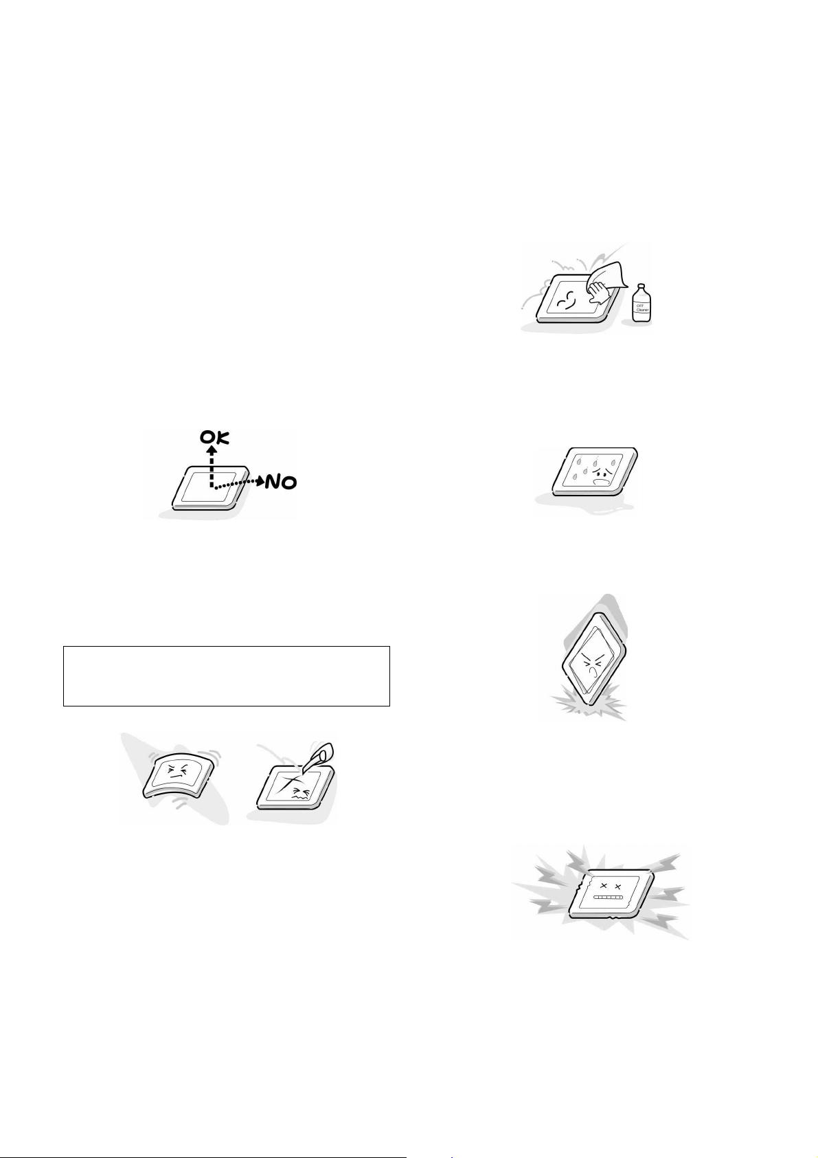
Precautions for Handling the LCD Module
The LCD module can easily be damaged during disassembly
or reassembly; therefore, always observe the following precautions when handling the module.
1. When attaching the LCD module to the LCD cover, position it appropriately and fasten at the position where the
display can be viewed most conveniently.
3. If the panel surface becomes soiled, wipe with cotton or a
soft cloth. If this does not remove the soiling, breathe on
the surface and then wipe again.
If the panel surface is extremely solied, use a CRT cleaner
as a cleaner. Wipe off the panel surface by drop the cleaner
on the cloth. Do not drop the cleaner on the panel. Pay
attention not to scratch the panel surface.
4. Leaving water or other fluids on the panel screen for an
extended period of time can result in discoloration or
stripes. Immediately remove any type of fluid from the
screen.
2. Carefully align the holes at all four corners of the LCD
module with the corresponding holes in the LCD cover
and fasten with screws. Do not strongly push on the module because any impact can adversely affect the performance. Also use caution when handling the polarized screen
because it can easily be damaged.
The metal edges of the LCD module
CAUTION
are sharp, so use caution to avoid injury.
5. Glass is used in the panel, so do not drop or strike with
hard objects. Such actions can damage the panel.
6. CMOS-LSI circuitry is used in the LCD module, so avoid
damage due to static electricity. When handling the module, use a wrist ground or anchor ground.
– 5 –
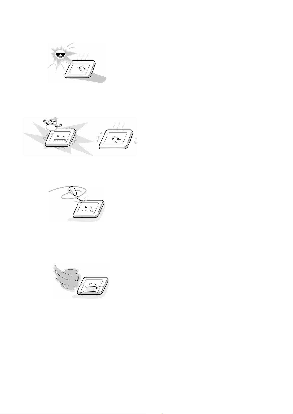
7. Do not expose the LCD module to direct sunlight or strong
ultraviolet rays for an extended period of time.
8. Do not store the LCD module below the temperature conditions described in the specifications. Failure to do so
could result in freezing of the liquid crystal due to cold air
or loss of resilience or other damage.
9. Do not disassemble the LCD module. Such actions could
result in improper operation.
10. When transporting the LCD module, do not use packing
containing epoxy resin (amine) or silicon resin (alcohol or
oxim). The gas generated by these materials can cause
loss of polarity.
– 6 –
SERVICE MODE
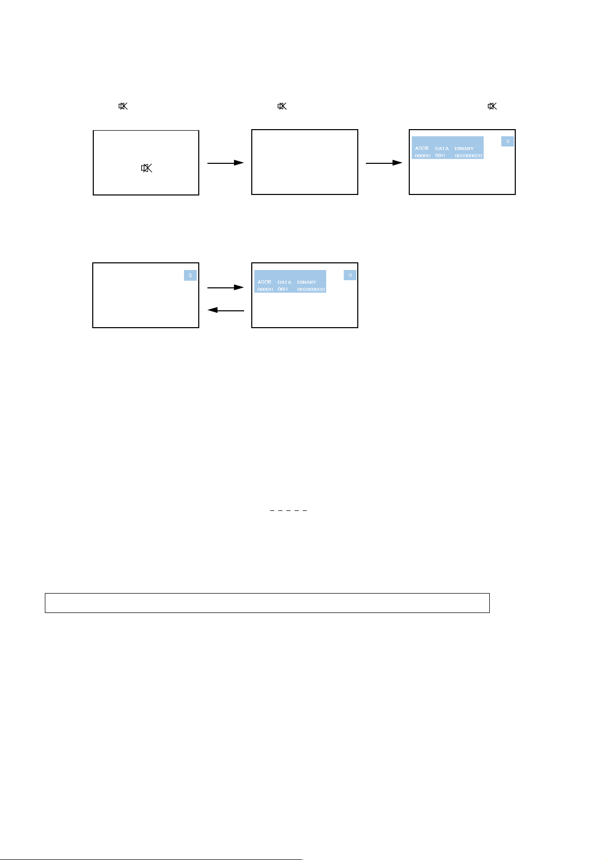
1. ENTERING SERVICE MODE
1) Press button once on 2) Press button again and 3) While pressing the button,
Remote Control. keep pressing. press MENU button on TV set.
or Sound Mute
2. DISPLAYING THE ADJUSTMENT MENU
1) Press MENU button on TV.
Service mode Adjustment mode
Press
Press
3. KEY FUNCTION IN THE SERVICE MODE
The following key entry during display of adjustment menu provides special functions.
(Service mode display)
Test signal selection : a button (on Remote)
Selection of the adjustment items : Channel s/t (on TV or Remote)
Change of the data value : Volume ; +/– (on TV or Remote)
Adjustment menu mode ON/OFF : MENU button (on TV)
Initialization of the memory : CALL + Channel button on TV (s)
Reset the count of operating protect
circuit to “00”: CALL + Channel button on TV (t)
“RCUT” selection : 1 button
“GCUT” selection : 2 button
“BCUT” selection : 3 button
“SCNT” selection : 4 button
“COLP” selection : 5 button
“TNTC” selection : 6 button
Automatic A/D Adjustment(PC, Component)
Self diagnostic display ON/OFF : 9 button
CAUTION : Never try to perform initialization unless you have changed the memory IC.
: 7 button
Color thickness correction
note: Displayed differently as shown below, de-
pending on the setting of the receiving color
system.
COLP (PAL)
COLC (NTSC)
COLS (SECAM)
– 7 –
4. SELECTING THE ADJUSTING ITEMS
1) Every pressing of CHANNEL s button in the service mode changes the adjustment items in the order of table-2.
(t button for reverse order)
5. ADJUSTING THE DATA
1) Pressing of VOLUME ; +/– button will change the value of data in the range from 00H to FFH. The variable range
depends on the adjusting item.
6. EXIT FROM SERVICE MODE
1) Pressing POWER button to turn off the TV once.
■ INITIALIZATION OF MEMORY DATA
After replacing EEPROM IC, the following initialization is required.
1. Enter the service mode, then select any register item.
2. Press and hold the CALL button on the Remote, then press the CHANNEL s button on theTV.The initialization of EEPROM IC
has been complated.
3. Check the picture carefully. If necessary, adjust any adjustment item above.
Perform “Auto tune” on the owner’s manual.
CAUTION: Never attempt to initialize the data unless EEPROM IC has been replaced.
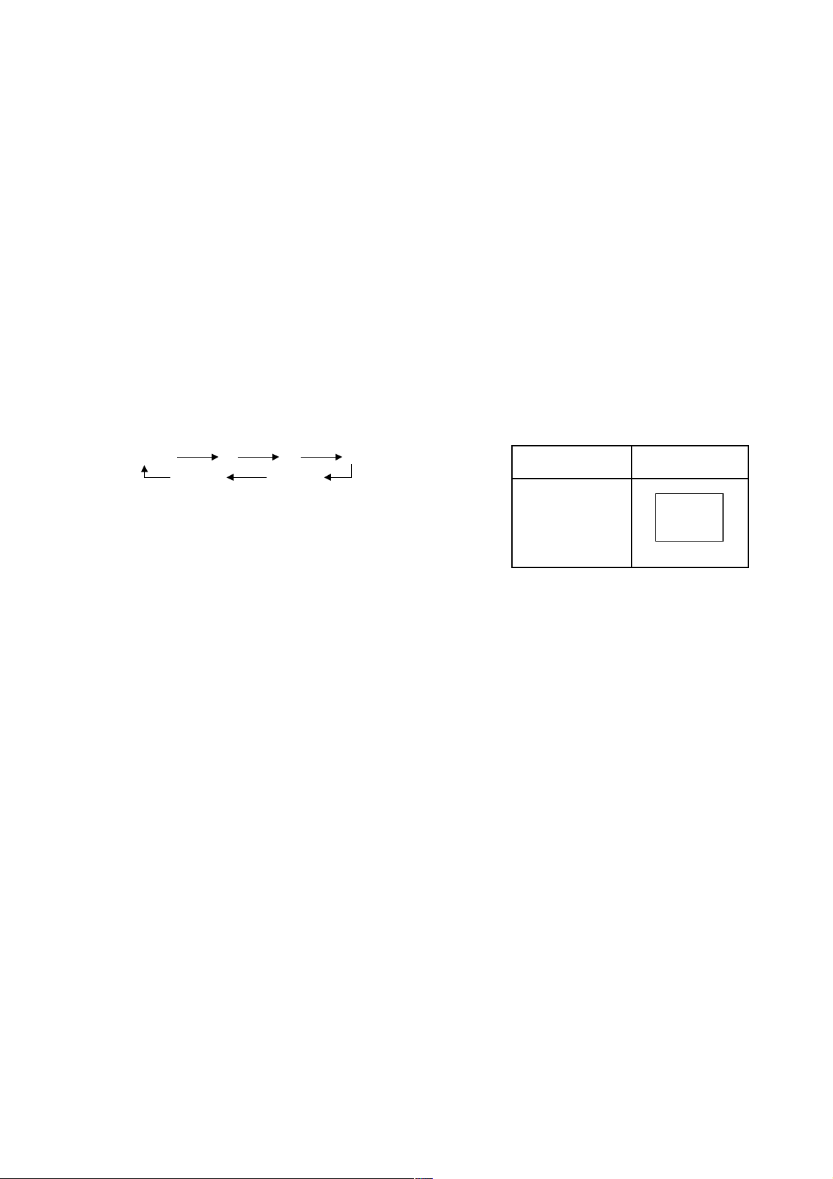
7. TEST SIGNAL SELECTION
1) Every pressing of a button on the Remote Control changes the built-in test patterns on screen as described below
in SERVICE MODE.
R
All BlackAll White
BSignal off G
Signals Picture
• Red raster
• Green raster
• Blue raster
• All Black
• All White
– 8 –
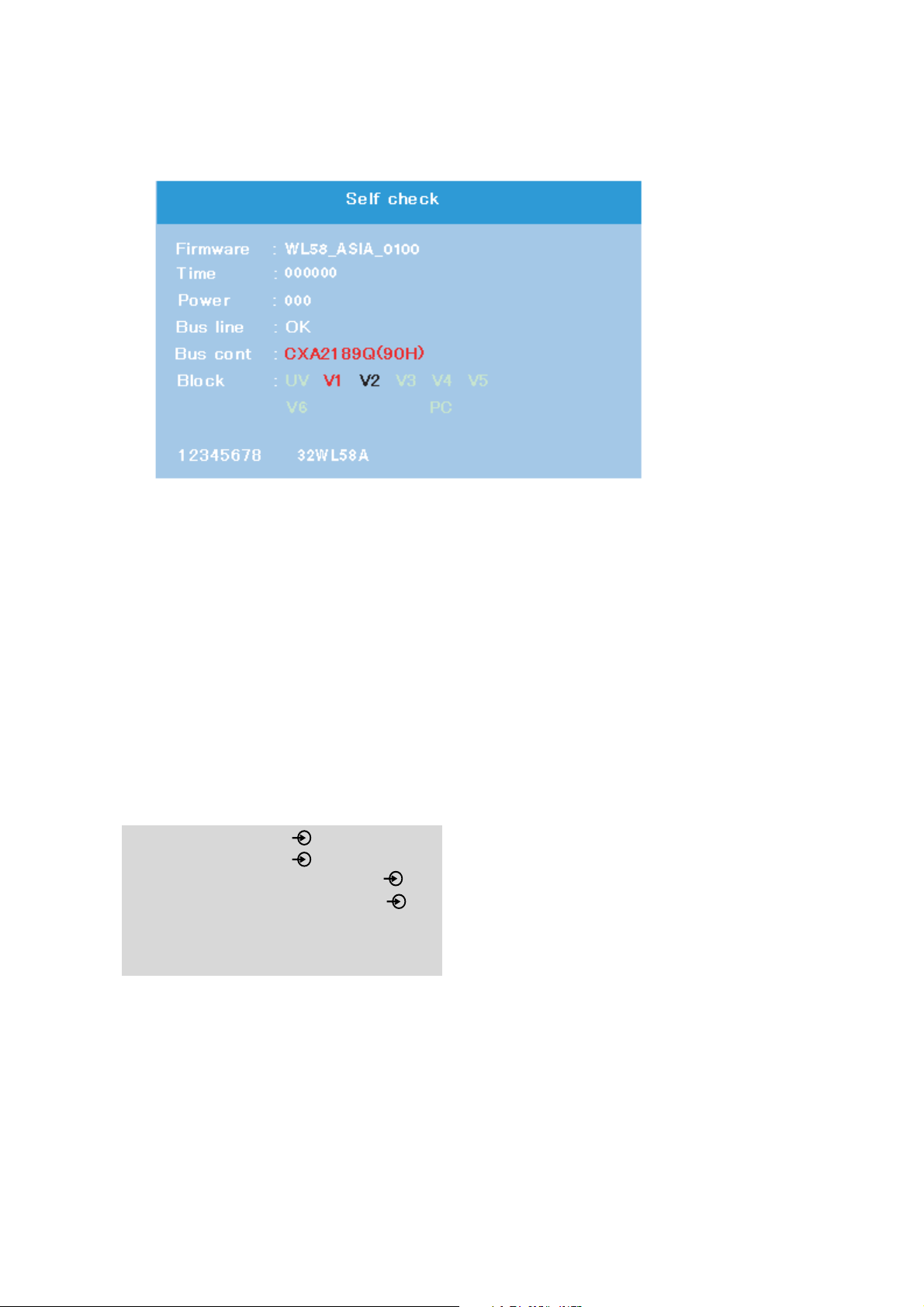
8. SELF DIAGNOSTIC FUNCTION
1) Press “9” button on Remote Control during display of adjustment menu in the service mode.
The diagnosis will begin to check if interface among IC’s is executed properly.
2) During diagnosis, the following displays are shown.
1
2
3
4
5
6
78
1
Firmware :
Version information of microprocessor
In case of file name : WL58_ASIA and Version : 0100 indicates[WL58_ASIA_0100].
2
Time : Total hour of turn the TV on. (Unit : H)
3
Power : Operation number of protecting circuit ----"000" is normal.
When indication is other than "000", overcurrent apt to flow, and circuit parts may possibly be damaged.
4
Bus line : --"OK" is normal
"SCL-GND"(Red indication) : SCL-GND short circuit
"SDA-GND"(Red indication) : SDA-GND short circuit
"SCL-SDA"(Red indication) : SCL-SDA short circuit
5
Bus cont : --- "OK" is normal.
NG is abnormal(Red indication), when
type name of semiconductor indicates.
Block
6
UV : TV reception mode
V1 : VIDEO 1 input mode ( 1)
V2 : VIDEO 2 input mode ( 2)
V3 : COMPONENT VIDEO1 input mode ( C1)
V4 : COMPONENT VIDEO 2 input mode ( C2)
V5 : HDMI 1 input mode
V6 : HDMI 2 input mode
PC : Personal Computer input mode
8 digit : CD number
7
Model name (7 digit)
8
– 9 –
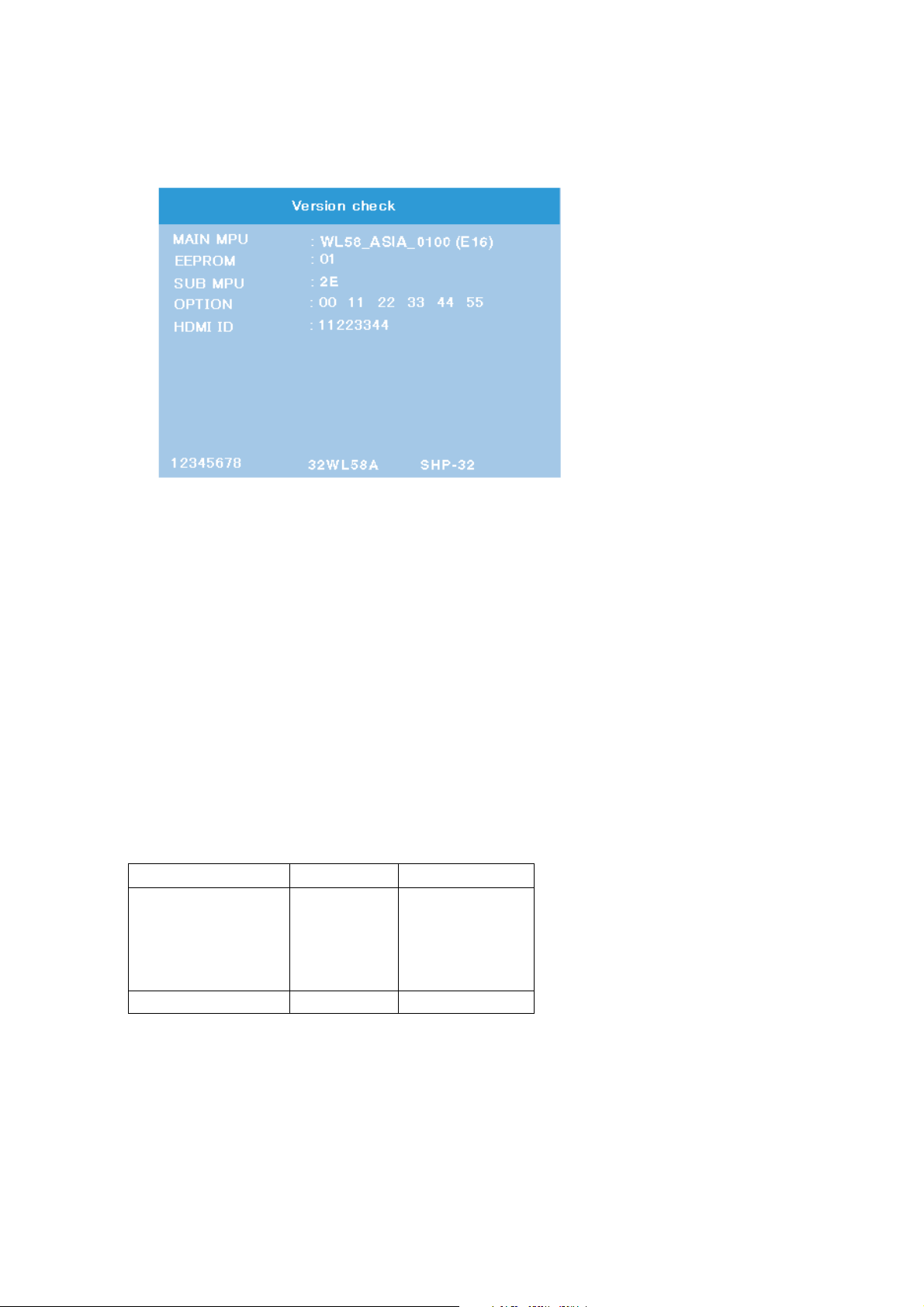
9. VERSION CHECK MODE
1) Press “9” button twice on Remote Control during display of adjustment menu in the service mode. The version of main
MPU will begin to check.
2) During Version Check, the following displays are shown.
M
N
O
P
Q
R
ST
M
MAIN MPU :
Version information of microprocessor
In case of file name : WL58_ASIA, Version 0100 for Code Program Version
and (E16) for OSD Version indicates [WL58_ASIA_0100(E16)]
N
EEPROM :
Version information of EEPROM : Display 1 byte data.
O
SUB MPU :
Version information of SUB MPU : Display 1 byte data.
P
OPTION :
Option information : Display six numbers of 1 byte data.
Q
HDMI ID :
HDMI ID information : Display 4 byte data.
R
CD number : Display 8 digit number
S
Model name : Display 7 digit number
T
Panel Vender information display
The following Panel Vender and screen size are displayed.
Panel
PDP
Example : SHP-32 indicates that Vender is SHP and Screen Size is 32 inch.
Panel Vender Screen Size(Inch)
LPLLCD
SHP -26
CMO
LG
-23
-32
-37
-42
-42
– 10 –
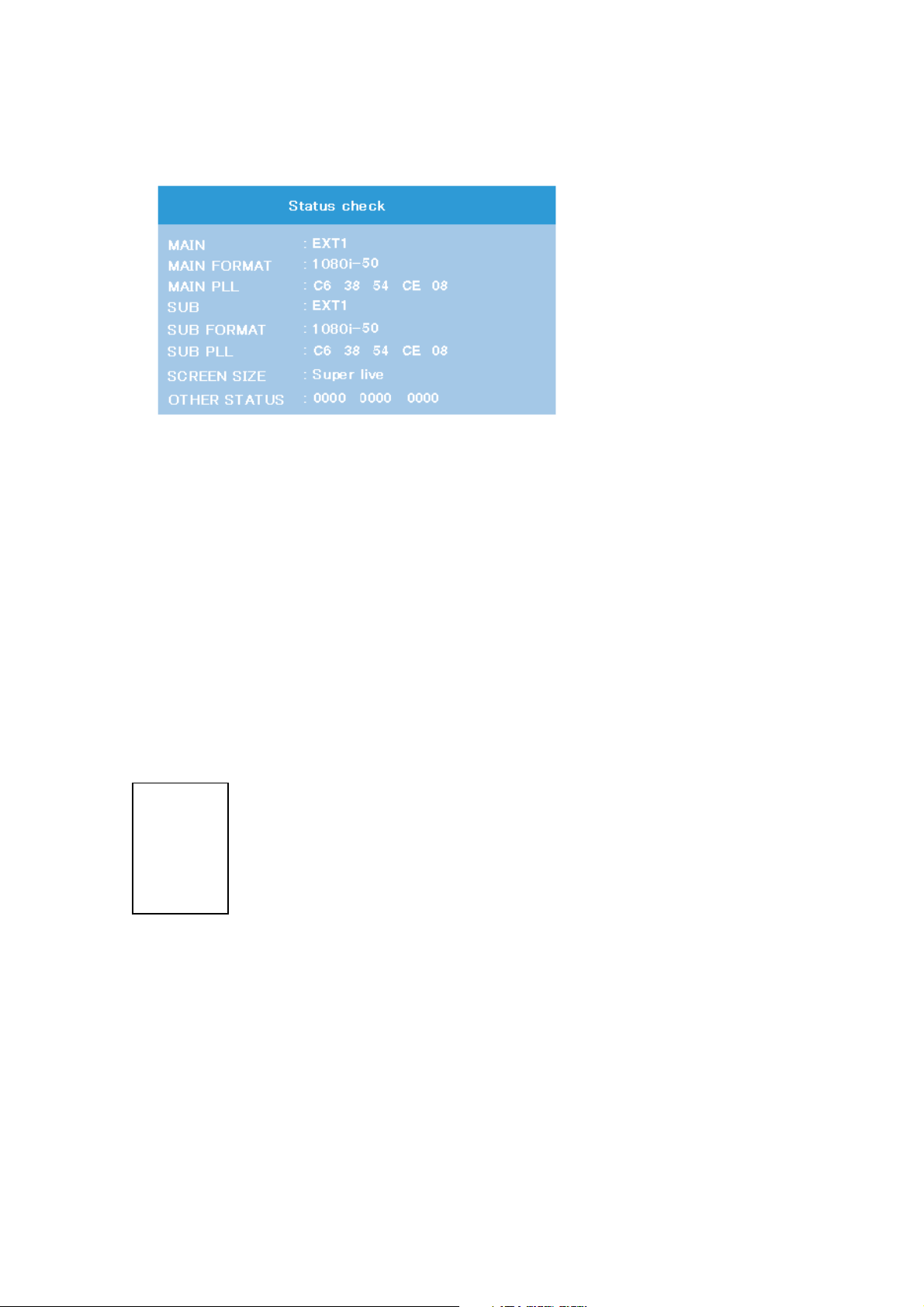
10. STATUS CHECK MODE
1) Press “9” button thrice on Remote Control during display of adjustment menu in the service mode. The status of this model
will begin to check.
2) During Status Check, the following displays are shown.
1
2
3
4
5
R
S
T
M
MAIN :
Main source information :
Display RF position number (0 - 99) on the main screen, or Input Source (EXT1/2/3/HDMI etc.)
MAIN FORMAT :
N
Display Video and PC format information
MAIN PLL :
O
Main PLL information : Display five numbers of 1 byte data.
SUB:
P
Sub source information :
Display RF position number (0 - 99) on the sub screen, or Input Source (EXT1/2/3/HDMI etc.)
SUB FORMAT :
Q
Display Video and PC format information
SUB PLL :
R
Sub PLL information : Display five numbers of 1 byte data.
SCREEN SIZE :
S
Display the screen size as follows.
Super live
Cinema
Subtitle
14:9
Wide
4:3
OTHER STATUS :
T
Other status information : Display three numbers of 2 byte data.
– 11 –
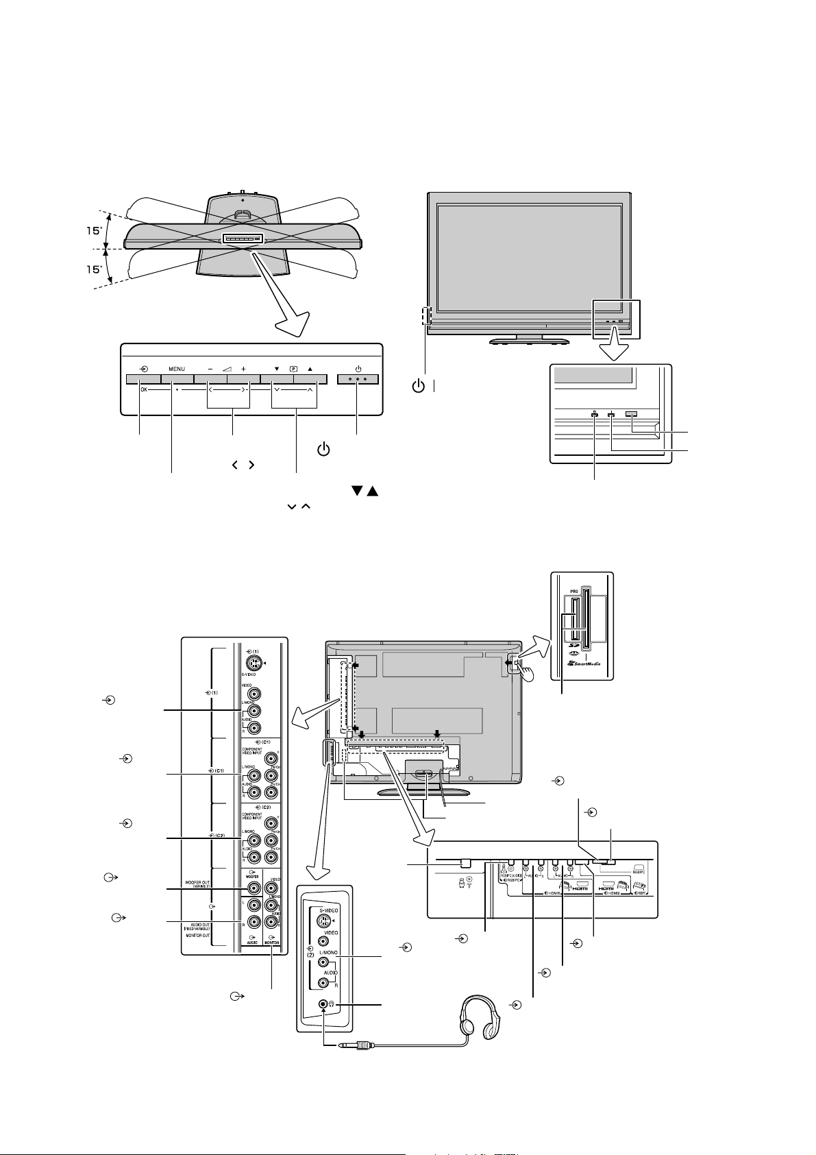
LOCATION OF CONTROLS
TV TOP VIEW
You can swivel the TV screen.
Swivel angle: 15 degrees to
left and right.
Input source
selection
Volume – +
Menu
MENU
Back
Top view
Power
Program position
Menu
TV FRONT VIEW
/ Power switch
Remote sensor
Power indicator
(red)
On-timer indicator
(green)
Left side view
(1) Video 1
input terminals
(C1)
COMPONENT
VIDEO INPUT
terminals
(C2)
COMPONENT
VIDEO INPUT
terminals
WOOFER
OUT terminal
AUDIO
OUT terminals
(Fixed/Variable)
Right side view TV back view
Antenna input
Right side
view
(2)
Video 2 input
terminals
MONITOR
OUT terminals
Headphone jack
(3.5 mm, stereo)
Power cord
Cable holder*
Back view
RGB/PC
(AUDIO)
input
Card into the slot
Squeeze tab and pull here
to open the door.
RGB/PC
input
HDMI 2
input terminal
HDMI 1
input terminal
HDMI 2 AUDIO
input terminals
HDMI 1 AUDIO
input terminals
– 12 –
Headphones
(Not supplied)
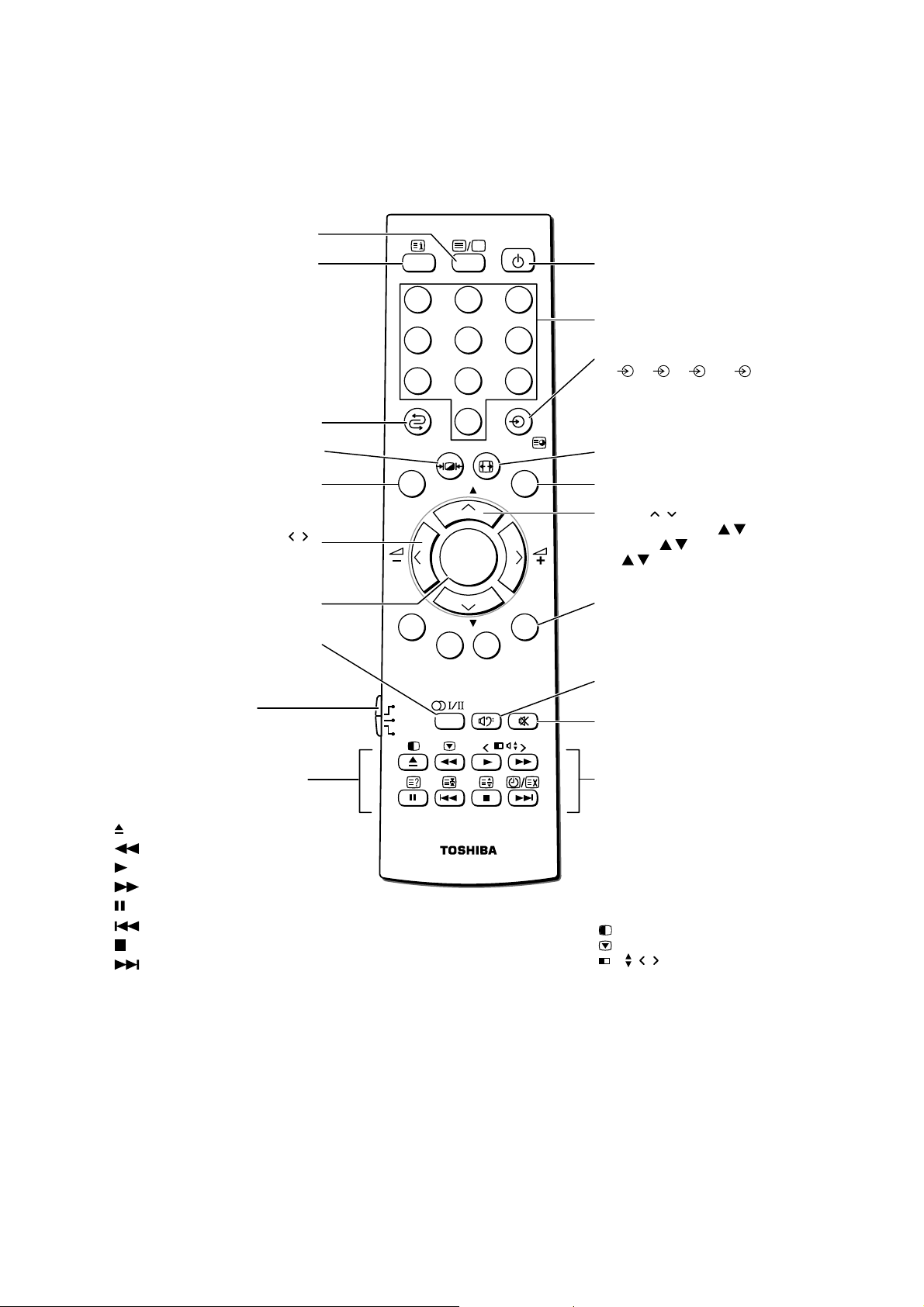
Remote control
Teletext on/off
Initial/index function for Teletext
CALL
To return to the previous program
Picture mode selection
MENU
DVD MENU
• Menu
• Volume – +
OK
Stereo/bilingual selection
Mode switch
TV : To control TV
VCR : To control VCR
DVD : To control DVD
When in VCR or DVD mode:
(Only for Toshiba VCR/DVD
players)
to EJECT
to REWIND
to PLAY
to FAST FORWARD
to PAUSE
to SKIP-REWIND
to STOP
to SKIP-FORWARD
CALL
MENU
DVD
MENU
TV
VCR
DVD
DVD
Power on/Standby
(For Toshiba TV/VCR/DVD)
1
2
3
Number buttons (0-9)
4
5
6
• Input source selection
(
1,
2,
C1,
7
8
9
HDMI 1, HDMI 2, PC, BM)
C2,
• To access sub-pages when in
0
teletext
Picture size selection
P
OK
EXIT
EXIT
• Menu
• Program position
• Teletext
• P
• Teletext control buttons
P
(Four colored buttons: Red,
Green, Yellow, Blue)
• BRIDGE MEDIA
• Bass boost on/off
• External woofer on/off
Sound mute
When in Teletext mode:
? To reveal concealed text
v To hold a wanted page
^
To enlarge teletext display size
CT-90241
y/X
When in TV mode:
y/X
To select a page while viewing
a normal picture
To select the time display
Double-Window on/off
Picture STILL
n
Double-Window
sound selection
picture/
– 13 –

LAYOUT OF MAJOR BOARDS
U003B
FRONT AV BOARD
U003G
PC HDMI BOARD
U003A
TN AV BOARD
U004
LOW B BOARD
U003D
KEY BOARD
U005
BRIDGE MEDIA BOARD
U001
SIGNAL BOARD
U003C
RMT LED BOARD
U002A
POWER BOARD
U003F
POWER SW BOARD
U002B
AC IN BOARD
– 14 –
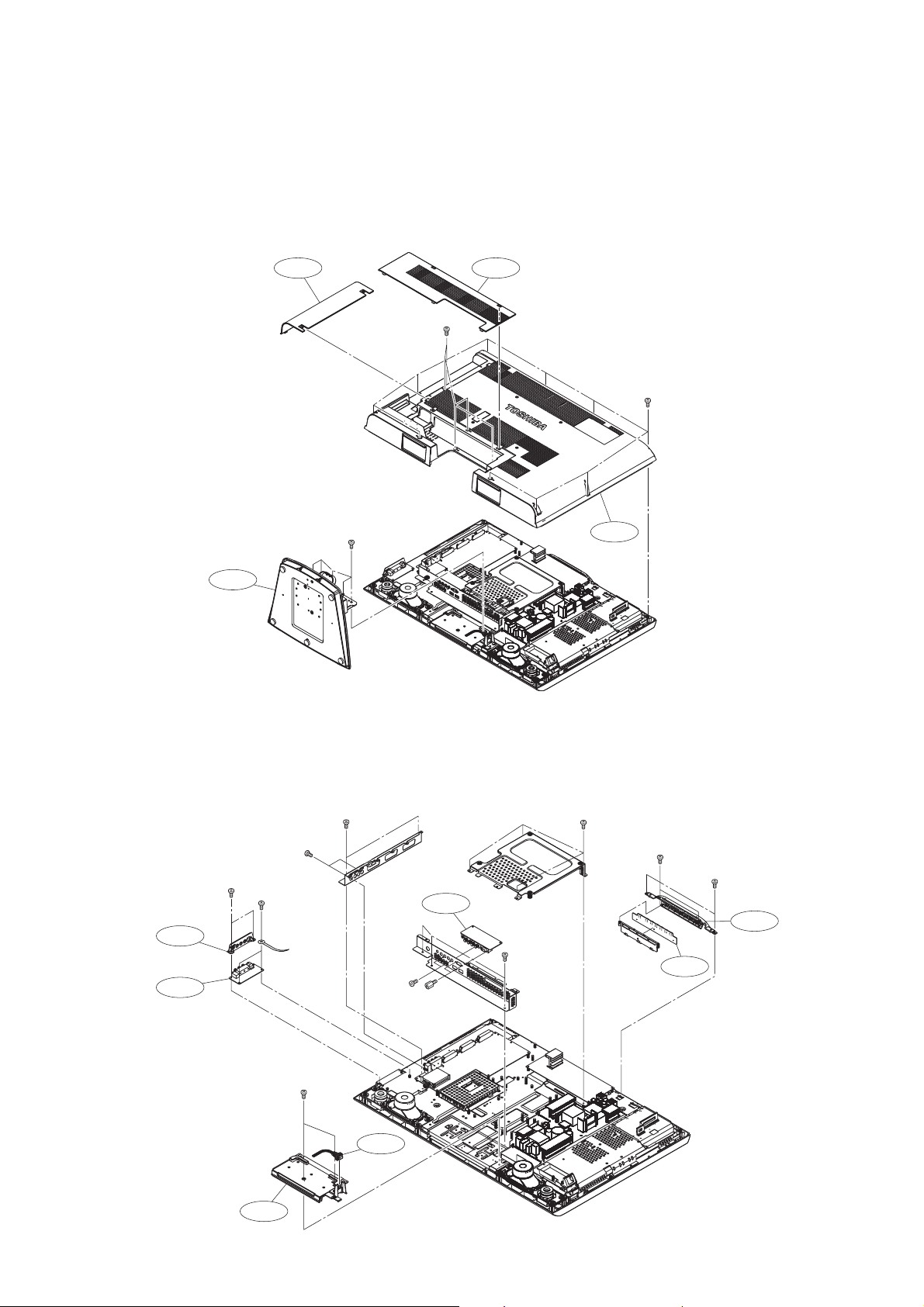
MECHANICAL DISASSEMBLY
1. Remove the stand (foot) and back cover.
A420
A450
PP 5×16 SW+W SBN
×5
A445
PP3×8
+SW+W SBN
×5
BITTB4×16 SBN
×10
A401
2. Remove the boards (FRONT AV,PC HDMI, KEY) and back center cover.
PP3×8+SW+W SBN
×2
PP3×8
+SW+W SBN
×2
PP3×8+SW+W SBN
×2
PP3×8+SW+W SBN
×2
A320
U003B
PP3×8+SW+W SBN
×2
PP3×8+SW+W SBN
×2
PP3×8
+SW+W SBN
×2
U003G
BITTB
3×12SBN
×2
P801
BITTB3×12SBN
×2
BITTB4×16 SBN
×2
U003D
A340
A315
– 15 –
3. Remove the boards (POWER, AC-IN, SIGNAL, LOW B, TN AV, RMT LED, BRIDGE MEDIA,
POWER SW) and speakers.
PP3×8+SW+W SBN
×6
U003A
BITTB3×12SBN
×3
U003C
BITTB4×16
SBN ×2
W661
W661
PP3×8
+SW+W SBN
×4
BITTB4×16
SBN ×2
U004
U001
U002B
PP3×8+SW+W SBN
×4
PP3×8
+SW+W SBN
×2
PP3×8
+SW+W SBN
×1
PP3×8+SW+W SBN
×8
U002A
PP3×8
+SW+W SBN
×4
U005
U003F
A331
PP3×8
+SW+W SBN
×4
PP3×8
+SW+W SBN
×1
4. Remove the display.
BITTB4×16 SBN
×2
BITTB4×16 SBN
×12
BITTB4×16 SBN
BITTB4×16 SBN
×2
BITTB4×16
SBN
BITTB4×16 SBN
×2
BITTB4×16 SBN
×2
B001
– 16 –
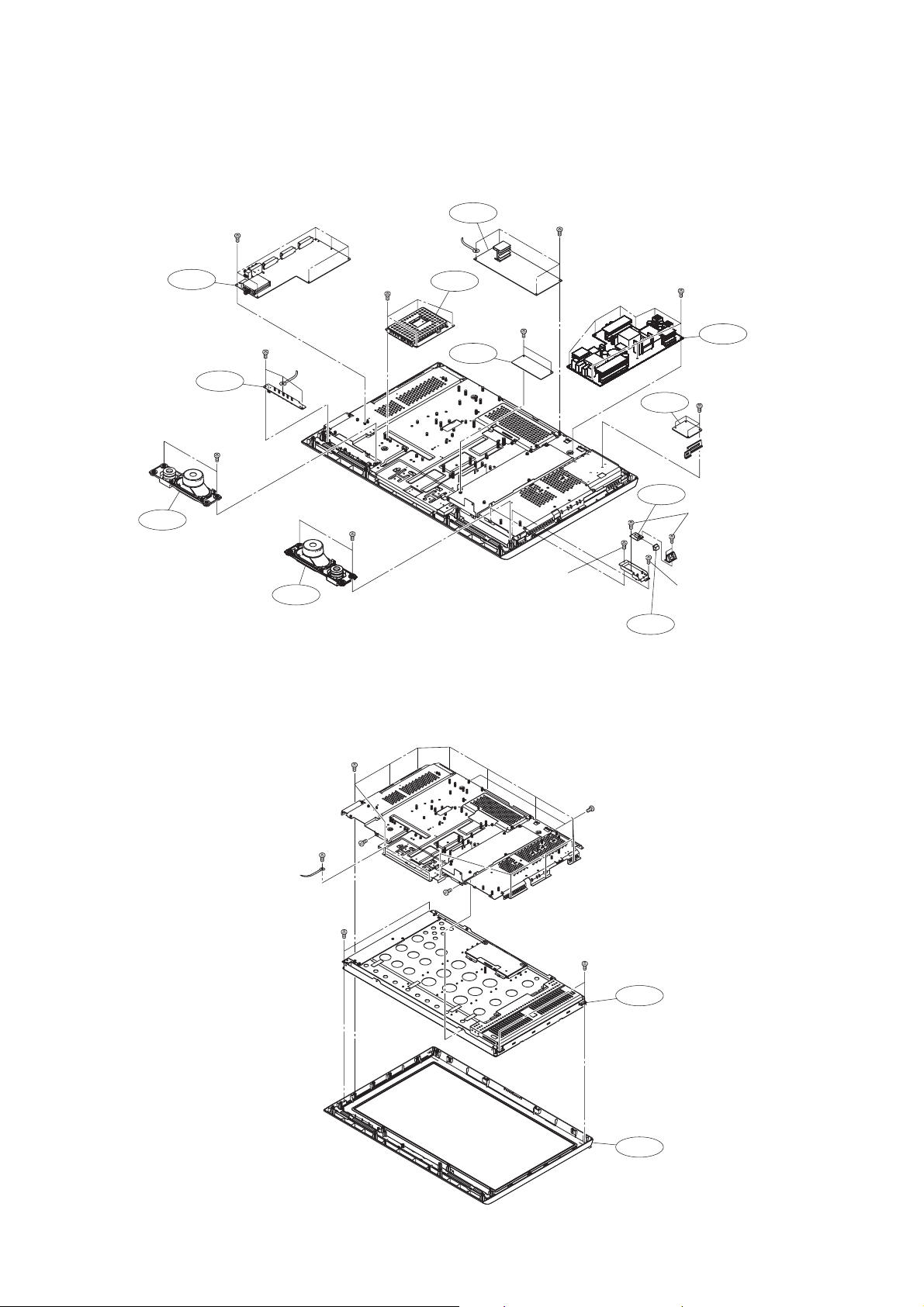
A201
1. Chassis Block
A450
EXPLODED VIEWS
A445
PP3×8+SW+W SBN
×5
BITTB4×16 SBN
×10
A401
PP3×8+SW+W SBN
×2
PP3×8+SW+W SBN
×2
PP3×8+SW+W SBN
×2
A320
U003B
PP 5×16 SW+W SBN
×5
PP3×8
+SW+W SBN
×2
BITTB3×12SBN
×2
U003G
PP3×8+SW+W SBN
×2
PP3×8+SW+W SBN
×2
A340
BITTB3×12SBN
×2
BITTB4×16 SBN
×2
U003D
U005
PP3×8
+SW+W SBN
×4
A420
– 17 –
PP3×8
+SW+W SBN
×1
U003F
A331
PP3×8
+SW+W SBN
×4
PP3×8
+SW+W SBN
×1
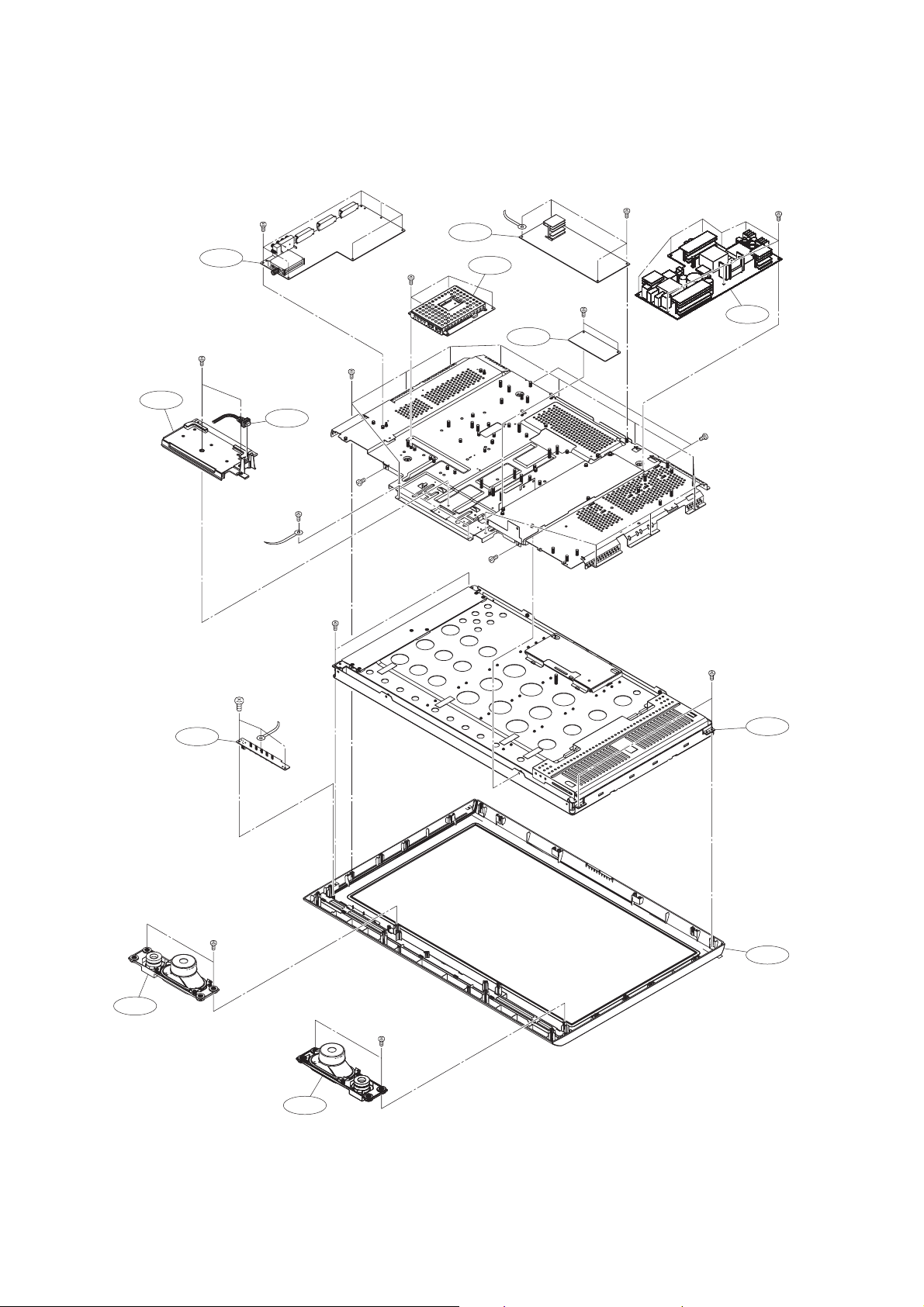
2. Main Block
PP3×8+SW+W SBN
×6
U003A
PP3×8+SW+W SBN
×2
A315
BITTB4×16 SBN
×12
P801
BITTB4×16 SBN
BITTB4×16 SBN
×2
BITTB4×16 SBN
×2
PP3×8+SW+W SBN
×4
BITTB4×16 SBN
U004
U001
PP3×8+SW+W SBN
×4
PP3×8+SW+W SBN
×2
U002B
PP3×8+SW+W SBN
×8
U002A
BITTB4×16 SBN
×2
W661
BITTB3×12SBN
×3
U003C
BITTB4×16 SBN
×2
W661
BITTB4×16 SBN
×2
BITTB4×16 SBN
×2
B001
A201
– 18 –
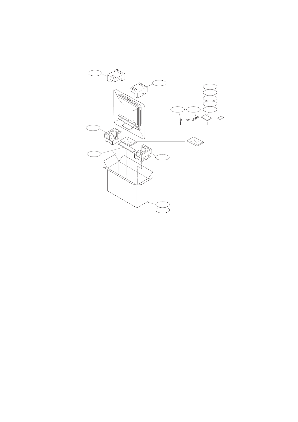
PACKING DISASSEMBLY
A702A
A702B
A709
A702A
A702B
A701
A701R
Y101M
Y101K
Y101J
Y101H
Y130Y170 Y101A
– 19 –
CHASSIS AND CABINET REPLACEMENT PARTS LIST
WARNING: BEFORE SERVICING THIS CHASSIS, READ THE "SERVICE SAFETY PRECAUTIONS" ON PAGE 3 OF
THIS MANUAL.
CAUTION: The international hazard symbols " " in the schematic diagram and the parts list designate components
which have special characteristics important for safety and should be replaced only with types identical to those in the
original circuit or specified in the parts list. The mounting position of replacements is to be identical with originals.
Before replacing any of these components, read carefully the PRODUCT SAFETY NOTICE. Do not degrade the safety
of the receiver through improper servicing.
NOTICE:
••
•
The part number must be used when ordering parts, in order to assist in processing, be sure to include the
••
Model number and Description.
••
•
The PC board assembly with * mark is no longer available after the end of the production.
••
Model : 32WL58A/32WL58E/32WL58R/32WL58T
Capacitors ............. CD : Ceramic Disk PF : Plastic Film EL : Electrolytic
Resistors ............... CF : Carbon Film CC : Carbon Composition MF : Metal Film
OMF : Oxide Metal Film VR : Variable Resistor FR : Fusible Resistor
(All CD and PF capacitors are
±5%, 50V and all resistors, ±5%, 1/6W unless otherwise noted.)
Location Parts No. Description
No.
#1 : [32WL58A]
#2 : [32WL58E]
#3 : [32WL58R]
#4 : [32WL58T]
CAPACITORS
C101 76109103 CERAMIC CHIP, 50V B 0.01UF K
C102 76073019 ELECTROLYTIC, 10V 470UF M 3A
C103 76109102 CERAMIC CHIP, 50V B 1000PF K
C104 76619143 ELECTROLYTIC CHIP, 50V 4.7UF M
C105 76073019 ELECTROLYTIC, 10V 470UF M 3A
C113 76109102 CERAMIC CHIP, 50V B 1000PF K
C117 76109103 CERAMIC CHIP, 50V B 0.01UF K
C118 76109103 CERAMIC CHIP, 50V B 0.01UF K
C162 76105101 CERAMIC CHIP, 50V CH 100PF J
C164 76100103 CERAMIC CHIP, 50V F 0.01UF Z
C190 76092730 CERAMIC CHIP, 16V B 0.1UF K
C501 76100104 CERAMIC CHIP, 25V F 0.1UF Z
C502 76100104 CERAMIC CHIP, 25V F 0.1UF Z
C503 76619046 ELECTROLYTIC CHIP, 16V 470UF
C504 76109103 CERAMIC CHIP, 50V B 0.01UF K
C505 76619046 ELECTROLYTIC CHIP, 16V 470UF
C506 76109103 CERAMIC CHIP, 50V B 0.01UF K
C507 76100104 CERAMIC CHIP, 25V F 0.1UF Z
C508 76100104 CERAMIC CHIP, 25V F 0.1UF Z
C509 76100104 CERAMIC CHIP, 25V F 0.1UF Z
C514 76665221 ELECTROLYTIC, 10V 220UF M 3A
C516 76105110 CERAMIC CHIP, 50V CH 11PF J
C517 76092785 CERAMIC CHIP, 10V B 0.47UF K
C519 76619048 ELECTROLYTIC CHIP, 25V 4.7UF M
C521 76092733 CERAMIC CHIP, 50V B 0.022UF K
C524 76109103 CERAMIC CHIP, 50V B 0.01UF K
C526 76109103 CERAMIC CHIP, 50V B 0.01UF K
C527 76619071 ELECTROLYTIC CHIP, 50V 2.2UF
C529 76100104 CERAMIC CHIP, 25V F 0.1UF Z
C530 76619157 ELECTROLYTIC CHIP, 16V 100UF
C605 76109102 CERAMIC CHIP, 50V B 1000PF K
C606 76109102 CERAMIC CHIP, 50V B 1000PF K
C607 76109103 CERAMIC CHIP, 50V B 0.01UF K
C612 76664102 ELECTROLYTIC, 6.3V 1000UF M 3A
C631 76619102 ELECTROLYTIC CHIP, 16V 47UF M
C632 76092731 CERAMIC CHIP, 16V B 1UF K
C633 76109103 CERAMIC CHIP, 50V B 0.01UF K
C634 76109103 CERAMIC CHIP, 50V B 0.01UF K
C640 76619100 ELECTROLYTIC CHIP, 16V 10UF M
C641 76666101 ELECTROLYTIC, 16V 100UF M 3A
Location Parts No. Description
No.
C642 76092731 CERAMIC CHIP, 16V B 1UF K
C643 76092731 CERAMIC CHIP, 16V B 1UF K
C644 76092731 CERAMIC CHIP, 16V B 1UF K
C645 76092731 CERAMIC CHIP, 16V B 1UF K
C647 76105221 CERAMIC CHIP, 50V CH 220PF J
C648 76105221 CERAMIC CHIP, 50V CH 220PF J
C649 76666470 ELECTORLYTIC, 16V 47UF M 3A
C650 76666470 ELECTORLYTIC, 16V 47UF M 3A
C651 76092463 CERAMIC CHIP, 16V B 0.22UF K
C652 76092463 CERAMIC CHIP, 16V B 0.22UF K
C653 76092538 CERAMIC CHIP, 10V F 1UF Z
C655 76109103 CERAMIC CHIP, 50V B 0.01UF K
C657 76092731 CERAMIC CHIP, 16V B 1UF K
C661 76109102 CERAMIC CHIP, 50V B 1000PF K
C662 76109102 CERAMIC CHIP, 50V B 1000PF K
C663 76619100 ELECTROLYTIC CHIP, 16V 10UF M
C665 76669479 ELECTROLYTIC, 50V 4.7UF M
C666 76669479 ELECTROLYTIC, 50V 4.7UF M
C671 76669100 ELECTROLYTIC, 50V 10UF M
C674 76669100 ELECTROLYTIC, 50V 10UF M
C677 76109681 CERAMIC CHIP, 50V B 680PF K
C678 76109681 CERAMIC CHIP, 50V B 680PF K
C680 76668102 ELECTROLYTIC, 35V 1000UF M 3A
C681 76668102 ELECTROLYTIC, 35V 1000UF M 3A
C682 76668102 ELECTROLYTIC, 35V 1000UF M 3A
C690 76815103 CERAMIC CHIP, 50V B 0.01UF K
C694 76285104 CERAMIC CHIP, 50V B 0.1UF K
C696 76285104 CERAMIC CHIP, 50V B 0.1UF K
C801 76168007 MT PLA AC275V 1UF M
C802 76503508 MT PLA PCX2 337 11474
C806 76092555 CERAMIC DISC, AC250V E 1000PF M
C807 76092555 CERAMIC DISC, AC250V E 1000PF M
C808 76092553 CERAMIC DISC, AC250V B 470PF K
C809 76092553 CERAMIC DISC, AC250V B 470PF K
C812 76109102 CERAMIC CHIP, 50V B 1000PF K
C814 76109102 CERAMIC CHIP, 50V B 1000PF K
C815 76073037 ELECTROLYTIC, 16V 47UF M 3A
C815A 23960136 ADHESIVE, SILICONE, TSE3843-W
C816 76109102 CERAMIC CHIP, 50V B 1000PF K
C817 76109102 CERAMIC CHIP, 50V B 1000PF K
C818 76669010 ELECTROLYTIC, 50V 1UF M
C819 76539684 PLASTIC FILM, 50V 0.68UF J
C820 76125010 CHEMICON CE69R 450V 270UF M 3H
C821 76125011 CHEMICON CE04R 450V 82UF M 4A
C822 76214103 CERAMIC DISC, 500V B 0.01UF K
C824 76168008 MT PLA 450V 1UF K
– 20 –
Location Parts No. Description
No.
C825 76168008 MT PLA 450V 1UF K
C826 76092339 CERAMIC DISC, 2KV 330PF K
C827 76092339 CERAMIC DISC, 2KV 330PF K
C840 76125009 CHEMICON 450V 47UF M
C843 76166001 CERAMIC DISK CC45 SL 3.15KV 47PF J
C844 76669479 ELECTROLYTIC, 50V 4.7UF M
C845 76073196 ELECTROLYTIC, 50V 22UF M 3A
C846 76073140 ELECTROLYTIC CE04P 10V 680UF M 3A
C847 76665471 ELECTROLYTIC, 10V 470UF M
C848 76214471 CERAMIC DISC, 500V B 470PF K
C849A 23960136 ADHESIVE, SILICONE, TSE3843-W
C860 76214103 CERAMIC DISC, 500V B 0.01UF K
C861 76503053 PLASTIC FILM, 63V 1UF J
C862 76669229 ELECTROLYTIC, 50V 2.2UF M
C863 76503049 PLASTIC FILM, 63V 0.47UF J
C864 76567224 PLASTIC FILM, 50V 0.22UF J
C865 76567224 PLASTIC FILM, 50V 0.22UF J
C866 76092341 CERAMIC DISC, 2KV R 470PF K
C868 76435221 CERAMIC DISC, 500V SL 220PF J
C869 76435221 CERAMIC DISC, 500V SL 220PF J
C870 76503425 PLASTIC FILM CQ92 3D2J473J-K5
C872 76073189 ELECTROLYTIC, 35V 1000UF M
C873 76073189 ELECTROLYTIC, 35V 1000UF M
C876 76073204 ELECTROLYTIC CE04P 50V 330UF M 3A
C877 76669229 ELECTROLYTIC, 50V 2.2UF M
C878 76503041 PLASTIC FILM , 63V 0.1UF J
C880 76503229 PLASTIC FILM, 1250VH 1000PF H
C881 76092337 CERAMIC DISC, 2KV 220PF K
C882 76567334 PLASTIC FILM, 50V 0.33UF J
C883 76212221 CERAMIC DISC, 50V B 220PF K
C884 76073196 ELECTROLYTIC, 50V 22UF M 3A
C885 76214471 CERAMIC DISC, 500V B 470PF K
C886 76212152 CERAMIC DISC, 50V B 1500PF K
C887 76214471 CERAMIC DISC, 500V B 470PF K
C888 76073189 ELECTROLYTIC, 35V 1000UF M
C889 76073189 ELECTROLYTIC, 35V 1000UF M
C890 76796102 ELECTROLYTIC, 35V 1000UF M
C891 76214471 CERAMIC DISC, 500V B 470PF K
C892 76676100 ELECTROLYTIC, 100V 10UF M 3A
C893 76747220 ELECTROLYTIC, 50V 22UF M 7L 3A
C894 76214471 CERAMIC DISC, 500V B 470PF K
C895 76073188 ELECTROLYTIC, 35V 680UF M
C896 76073188 ELECTROLYTIC, 35V 680UF M
C897 76796102 ELECTROLYTIC, 35V 1000UF M
C898 76669010 ELECTROLYTIC, 50V 1UF M
C1801 76285104 CERAMIC CHIP, 50V B 0.1UF K
C1802 76109103 CERAMIC CHIP, 50V B 0.01UF K
C1805 76109103 CERAMIC CHIP, 50V B 0.01UF K
C1806 76109103 CERAMIC CHIP, 50V B 0.01UF K
C1807 76109103 CERAMIC CHIP, 50V B 0.01UF K
C1808 76109103 CERAMIC CHIP, 50V B 0.01UF K
C1809 76109103 CERAMIC CHIP, 50V B 0.01UF K
C1810 76109103 CERAMIC CHIP, 50V B 0.01UF K
C1811 76109103 CERAMIC CHIP, 50V B 0.01UF K
C3212 76105620 CERAMIC CHIP, 50V CH 62PF J
C3242 76105620 CERAMIC CHIP, 50V CH 62PF J
C3272 76105620 CERAMIC CHIP, 50V CH 62PF J
C4222 76092538 CERAMIC CHIP, 10V F 1UF Z
C4406 76109103 CERAMIC CHIP, 50V B 0.01UF K
C4407 76109103 CERAMIC CHIP, 50V B 0.01UF K
C4408 76092538 CERAMIC CHIP, 10V F 1UF Z
C4409 76666471 ELECTROLYTIC, 16V 470UF M
C4410 76109103 CERAMIC CHIP, 50V B 0.01UF K
C5440 76109103 CERAMIC CHIP, 50V B 0.01UF K
C8171 76092730 CERAMIC CHIP, 16V B 0.1UF K
C8191 76092730 CERAMIC CHIP, 16V B 0.1UF K
C8210 76105331 CERAMIC CHIP, 50V CH 330PF J
C8211 76815473 CERAMIC CHIP, 50V B 0.047UF K
C8212 76092178 CERAMIC CHIP, 25V B 0.1UF K
C8213 76109102 CERAMIC CHIP, 50V B 1000PF K
C8241 76073196 ELECTROLYTIC, 50V 22UF M 3A
C8250 76092341 CERAMIC DISC, 2KV R 470PF K
C8251 76434100 CERAMIC DISC, 500V SL 10PF D
C8390 76109102 CERAMIC CHIP, 50V B 1000PF K
C8401 76092733 CERAMIC CHIP, 50V B 0.022UF K
C8402 76092733 CERAMIC CHIP, 50V B 0.022UF K
Location Parts No. Description
No.
C8403 76669470 ELECTROLYTIC, 50V 47UF M
C8490 76669010 ELECTROLYTIC, 50V 1UF M
C8601 76591682 PLASTIC FILM, 50V 6800PF J
C8602 76212101 CERAMIC DISC, 50V B 100PF K
C8605 76285104 CERAMIC CHIP, 50V B 0.1UF K
C8701 76567224 PLASTIC FILM, 50V 0.22UF J
C8702 76287224 CHIP CER 50V F 224Z GRM319F11H224ZA01D
C8703 76109102 CERAMIC CHIP, 50V B 1000PF K
C8801 76092730 CERAMIC CHIP, 16V B 0.1UF K
C8802 76092883 CERAMIC CHIP, 50V B 0.1UF K
C8891 76503049 PLASTIC FILM, 63V 0.47UF J
CB01 76202221 ELECTROLYTIC, 10V 220UF M 7L 3A
CB02 76202221 ELECTROLYTIC, 10V 220UF M 7L 3A
CB03 76100104 CERAMIC CHIP, 25V F 0.1UF Z
CB04 76100104 CERAMIC CHIP, 25V F 0.1UF Z
CB05 76202221 ELECTROLYTIC, 10V 220UF M 7L 3A
CB38 76100104 CERAMIC CHIP, 25V F 0.1UF Z
CC11 76109102 CERAMIC CHIP, 50V B 1000PF K
CC12 76109102 CERAMIC CHIP, 50V B 1000PF K
CC21 76109102 CERAMIC CHIP, 50V B 1000PF K
CC31 76109102 CERAMIC CHIP, 50V B 1000PF K
CC62 76109102 CERAMIC CHIP, 50V B 1000PF K
CC63 76109102 CERAMIC CHIP, 50V B 1000PF K
CC66 76109102 CERAMIC CHIP, 50V B 1000PF K
CC67 76109102 CERAMIC CHIP, 50V B 1000PF K
CC71 76109102 CERAMIC CHIP, 50V B 1000PF K
CC74 76109102 CERAMIC CHIP, 50V B 1000PF K
CC75 76109102 CERAMIC CHIP, 50V B 1000PF K
CC76 76109102 CERAMIC CHIP, 50V B 1000PF K
CC79 76109102 CERAMIC CHIP, 50V B 1000PF K
CC82 76109102 CERAMIC CHIP, 50V B 1000PF K
CC141 76109102 CERAMIC CHIP, 50V B 1000PF K
CC151 76109102 CERAMIC CHIP, 50V B 1000PF K
CC161 76109102 CERAMIC CHIP, 50V B 1000PF K
CC171 76109102 CERAMIC CHIP, 50V B 1000PF K
CC401 76109102 CERAMIC CHIP, 50V B 1000PF K
CC411 76109102 CERAMIC CHIP, 50V B 1000PF K
CE05 76073090 ELECTROLYTIC, 50V 100UF M 3A
CE10 76666470 ELECTORLYTIC, 16V 47UF M 3A
CE11 76539474 PLASTIC FILM, 50V 0.47UF J
CE12 76666470 ELECTORLYTIC, 16V 47UF M 3A
CE60 76073186 ELECTROLYTIC, 35V 470UF M
CE61 76617028 ELECTROLYTIC, 16V 1200UF M
CE62 76073020 ELECTROLYTIC, 10V 1000UF M 3A
CE63 76539104 PLASTIC FILM, 50V 0.1UF J
CE64 76539104 PLASTIC FILM, 50V 0.1UF J
CE65 76666470 ELECTORLYTIC, 16V 47UF M 3A
CE66 76539474 PLASTIC FILM, 50V 0.47UF J
CE67 76666470 ELECTORLYTIC, 16V 47UF M 3A
CE90 76073186 ELECTROLYTIC, 35V 470UF M
CE91 76617028 ELECTROLYTIC, 16V 1200UF M
CE92 76666471 ELECTROLYTIC, 16V 470UF M
CE93 76539104 PLASTIC FILM, 50V 0.1UF J
CE94 76539104 PLASTIC FILM, 50V 0.1UF J
CE95 76668101 ELECTROLYTIC, 35V 100UF M 3A
CS01 76092731 CERAMIC CHIP, 16V B 1UF K
CS02 76092515 CERAMIC CHIP, 16V F 4.7UF Z
CS03 76092726 CERAMIC CHIP, 10V B 2.2UF K
CS04 76092726 CERAMIC CHIP, 10V B 2.2UF K
CS05 76092726 CERAMIC CHIP, 10V B 2.2UF K
CS06 76092726 CERAMIC CHIP, 10V B 2.2UF K
CS08 76092611 CERAMIC CHIP, 6.3V B 2.2UF K
CS09 76092611 CERAMIC CHIP, 6.3V B 2.2UF K
CS10 76092628 CERAMIC CHIP, 6.3V B 10UF K
CS11 76092628 CERAMIC CHIP, 6.3V B 10UF K
CS12 76109473 CERAMIC CHIP, 25V B 0.047UF K
CS15 76092628 CERAMIC CHIP, 6.3V B 10UF K
CS16 76092628 CERAMIC CHIP, 6.3V B 10UF K
CS26 76619100 ELECTROLYTIC CHIP, 16V 10UF M
CS39 76092573 CERAMIC CHIP, 16V B 0.47UF K
CS40 76092611 CERAMIC CHIP, 6.3V B 2.2UF K
CS41 76092611 CERAMIC CHIP, 6.3V B 2.2UF K
CS42 76092611 CERAMIC CHIP, 6.3V B 2.2UF K
CS43 76092611 CERAMIC CHIP, 6.3V B 2.2UF K
CS44 76092611 CERAMIC CHIP, 6.3V B 2.2UF K
CS45 76092611 CERAMIC CHIP, 6.3V B 2.2UF K
– 21 –
Location Parts No. Description
No.
CS46 76092611 CERAMIC CHIP, 6.3V B 2.2UF K
CS47 76092611 CERAMIC CHIP, 6.3V B 2.2UF K
CS48 76092611 CERAMIC CHIP, 6.3V B 2.2UF K
CS49 76092611 CERAMIC CHIP, 6.3V B 2.2UF K
CS50 76092611 CERAMIC CHIP, 6.3V B 2.2UF K
CS51 76092611 CERAMIC CHIP, 6.3V B 2.2UF K
CS52 76092611 CERAMIC CHIP, 6.3V B 2.2UF K
CS53 76092611 CERAMIC CHIP, 6.3V B 2.2UF K
CS54 76092611 CERAMIC CHIP, 6.3V B 2.2UF K
CS55 76092611 CERAMIC CHIP, 6.3V B 2.2UF K
CS56 76092611 CERAMIC CHIP, 6.3V B 2.2UF K
CS57 76619102 ELECTROLYTIC CHIP, 16V 47UF M
CS62 76092611 CERAMIC CHIP, 6.3V B 2.2UF K
CS64 76619101 ELECTROLYTIC CHIP, 16V 22UF M
CS82 76092611 CERAMIC CHIP, 6.3V B 2.2UF K
CS83 76092611 CERAMIC CHIP, 6.3V B 2.2UF K
CS85 76092611 CERAMIC CHIP, 6.3V B 2.2UF K
CS86 76092611 CERAMIC CHIP, 6.3V B 2.2UF K
CT01 76092790 CERAMIC CHIP CK732B 6.3V 10UF K
CT04 76105820 CERAMIC CHIP, 50V CH 82PF J
CT05 76092731 CERAMIC CHIP, 16V B 1UF K
CT06 76092790 CERAMIC CHIP CK732B 6.3V 10UF K
CT07 76092790 CERAMIC CHIP CK732B 6.3V 10UF K
CT10 76105151 CERAMIC CHIP, 50V CH 150PF J
CT11 76092731 CERAMIC CHIP, 16V B 1UF K
CT12 76092790 CERAMIC CHIP CK732B 6.3V 10UF K
CT13 76092790 CERAMIC CHIP CK732B 6.3V 10UF K
CT16 76105151 CERAMIC CHIP, 50V CH 150PF J
CT17 76092731 CERAMIC CHIP, 16V B 1UF K
CT18 76092790 CERAMIC CHIP CK732B 6.3V 10UF K
CT19 76092790 CERAMIC CHIP CK732B 6.3V 10UF K
CT20 76092789 CERAMIC CHIP, 6.3V B 1UF K
CV01 76666471 ELECTROLYTIC, 16V 470UF M
CV02 76100104 CERAMIC CHIP, 25V F 0.1UF Z
CV03 76100104 CERAMIC CHIP, 25V F 0.1UF Z
CV04 76100104 CERAMIC CHIP, 25V F 0.1UF Z
CV07 76100104 CERAMIC CHIP, 25V F 0.1UF Z
CV09 76092731 CERAMIC CHIP, 16V B 1UF K
CV10 76100104 CERAMIC CHIP, 25V F 0.1UF Z
CV12 76092731 CERAMIC CHIP, 16V B 1UF K
CV16 76092731 CERAMIC CHIP, 16V B 1UF K
CV17 76092731 CERAMIC CHIP, 16V B 1UF K
CV18 76100104 CERAMIC CHIP, 25V F 0.1UF Z
CV19 76092731 CERAMIC CHIP, 16V B 1UF K
CV20 76092731 CERAMIC CHIP, 16V B 1UF K
CV21 76092731 CERAMIC CHIP, 16V B 1UF K
CV22 76092731 CERAMIC CHIP, 16V B 1UF K
CV23 76092731 CERAMIC CHIP, 16V B 1UF K
CV24 76092731 CERAMIC CHIP, 16V B 1UF K
CV25 76092731 CERAMIC CHIP, 16V B 1UF K
CV26 76092731 CERAMIC CHIP, 16V B 1UF K
CV27 76092731 CERAMIC CHIP, 16V B 1UF K
CV28 76092731 CERAMIC CHIP, 16V B 1UF K
CV29 76092731 CERAMIC CHIP, 16V B 1UF K
CV33 76100104 CERAMIC CHIP, 25V F 0.1UF Z
CV40 76100104 CERAMIC CHIP, 25V F 0.1UF Z
CV41 76100104 CERAMIC CHIP, 25V F 0.1UF Z
CV42 76100104 CERAMIC CHIP, 25V F 0.1UF Z
CV50 76619102 ELECTROLYTIC CHIP, 16V 47UF M
CV53 76100104 CERAMIC CHIP, 25V F 0.1UF Z
CV56 76619157 ELECTROLYTIC CHIP, 16V 100UF
CV59 76666471 ELECTROLYTIC, 16V 470UF M
CV62 76100104 CERAMIC CHIP, 25V F 0.1UF Z
CV63 76666471 ELECTROLYTIC, 16V 470UF M
CV72 76619101 ELECTROLYTIC CHIP, 16V 22UF M
CV74 76092731 CERAMIC CHIP, 16V B 1UF K
CV121 76109103 CERAMIC CHIP, 50V B 0.01UF K
CV122 76105101 CERAMIC CHIP, 50V CH 100PF J
CY01 76100104 CERAMIC CHIP, 25V F 0.1UF Z
CY02 76100104 CERAMIC CHIP, 25V F 0.1UF Z
CY03 76100104 CERAMIC CHIP, 25V F 0.1UF Z
CY101 76109103 CERAMIC CHIP, 50V B 0.01UF K
CY102 76073019 ELECTROLYTIC, 10V 470UF M 3A
CY103 76109102 CERAMIC CHIP, 50V B 1000PF K
CY113 76109102 CERAMIC CHIP, 50V B 1000PF K
CY190 76092730 CERAMIC CHIP, 16V B 0.1UF K
Location Parts No. Description
No.
CY650 76109103 CERAMIC CHIP, 50V B 0.01UF K
RESISTORS
R101 76011101 CHIP, 1/20W 100 OHM J
R102 76011101 CHIP, 1/20W 100 OHM J
R103 76011101 CHIP, 1/20W 100 OHM J
R104 76011103 CHIP, 1/20W 10K OHM J
R105 76011273 CHIP, 1/20W 27K OHM J
R107 76000445 CHIP JUMPER, 1608TYPE
R108 76000445 CHIP JUMPER, 1608TYPE
R114 76000445 CHIP JUMPER, 1608TYPE
R123 76011101 CHIP, 1/20W 100 OHM J
R124 76011101 CHIP, 1/20W 100 OHM J
R167 76011101 CHIP, 1/20W 100 OHM J
R169 76000445 CHIP JUMPER, 1608TYPE
R170 76011682 CHIP, 1/20W 6.8K OHM J
R229 76872750 CHIP, 1/16W 75 OHM J
R501 76011682 CHIP, 1/20W 6.8K OHM J
R502 76011272 CHIP, 1/20W 2.7K OHM J
R504 76011101 CHIP, 1/20W 100 OHM J
R505 76011101 CHIP, 1/20W 100 OHM J
R506 76011273 CHIP, 1/20W 27K OHM J
R507 76011392 CHIP, 1/20W 3.9K OHM J
R508 76011682 CHIP, 1/20W 6.8K OHM J
R512 76011101 CHIP, 1/20W 100 OHM J
R514 76011102 CHIP, 1/20W 1K OHM J
R607 76011223 CHIP, 1/20W 22K OHM J
R620 76011223 CHIP, 1/20W 22K OHM J
R621 76011472 CHIP, 1/20W 4.7K OHM J
R625 76871151 CHIP, 1/8W 150 OHM J
R626 76871151 CHIP, 1/8W 150 OHM J
R627 76011473 CHIP, 1/20W 47K OHM J
R628 76011473 CHIP, 1/20W 47K OHM J
R629 76011103 CHIP, 1/20W 10K OHM J
R630 76011103 CHIP, 1/20W 10K OHM J
R631 76871750 CHIP, 1/8W 75 OHM J
R632 76871750 CHIP, 1/8W 75 OHM J
R640 76011101 CHIP, 1/20W 100 OHM J
R641 76011101 CHIP, 1/20W 100 OHM J
R644 76011102 CHIP, 1/20W 1K OHM J
R645 76011102 CHIP, 1/20W 1K OHM J
R646 76011473 CHIP, 1/20W 47K OHM J
R647 76011473 CHIP, 1/20W 47K OHM J
R648 76871151 CHIP, 1/8W 150 OHM J
R649 76871151 CHIP, 1/8W 150 OHM J
R650 76011102 CHIP, 1/20W 1K OHM J
R651 76011473 CHIP, 1/20W 47K OHM J
R652 76011103 CHIP, 1/20W 10K OHM J
R653 76011223 CHIP, 1/20W 22K OHM J
R654 76011103 CHIP, 1/20W 10K OHM J
R655 76011222 CHIP, 1/20W 2.2K OHM J
R656 76011103 CHIP, 1/20W 10K OHM J
R664 76011104 CHIP, 1/20W 100K OHM J
R665 76011104 CHIP, 1/20W 100K OHM J
R667 76011104 CHIP, 1/20W 100K OHM J
R670 76011472 CHIP, 1/20W 4.7K OHM J
R671 76011182 CHIP, 1/20W 1.8K OHM J
R672 76011472 CHIP, 1/20W 4.7K OHM J
R673 76011182 CHIP, 1/20W 1.8K OHM J
R675 76011102 CHIP, 1/20W 1K OHM J
R676 76011473 CHIP, 1/20W 47K OHM J
R677 76011473 CHIP, 1/20W 47K OHM J
R684 76871229 CHIP, 1/8W 2.2 OHM J
R685 76871229 CHIP, 1/8W 2.2 OHM J
R697 76000576 CHIP JUMPER, 3216TYPE
R801 76017004 METAL GLAZE 1/2W 510K J
R809 76004718 METAL GLAZE, 1/2W 8.2M OHM J
R812 76011473 CHIP, 1/20W 47K OHM J
R820 76019461 METAL PLATE, 2W 0.15 OHM J
R821 76019461 METAL PLATE, 2W 0.15 OHM J
R826 76004714 METAL GLAZE, 1/2W 1.2M OHM J
R830 76007061 CERAMIC COVERED, 2W 1.8 OHM K
R831 76120003 CERAMIC COVERED G 5W 4.7 J
R840 76382823 0XIDE FILM 1W 82K J
R841 76322339 METAL FILM 1W 3R3 J
R842 76310479 OXIDE METAL FILM, 1/2W 4.7 OHM J
– 22 –

Location Parts No. Description
No.
R860 76552271 OXIDE METAL FILM, 1/2W 270 OHM J
R862 76552681 OXIDE METAL FILM, 1/2W 680 OHM J
R863 76011272 CHIP, 1/20W 2.7K OHM J
R864 76552101 OXIDE METAL FILM, 1/2W 100 OHM J
R865 76552100 OXIDE METAL FILM, 1/2W 10 OHM J
R867 76552330 OXIDE METAL FILM, 1/2W 33 OHM J
R880 76553683 OXIDE METAL FILM, 1W 68K OHM J
R881 76553683 OXIDE METAL FILM, 1W 68K OHM J
R882 76323569 METAL FILM 2W 5R6 J
R883 76079010 METAL RES 2W R47 J
R884 76321339 OXIDE METAL FILM, 1/2W 3.3 OHM J
R885 76553101 OXIDE METAL FILM, 1W 100 OHM J
R886 76554432 OXIDE FILM 2W 4.3K J
R4100 76011102 CHIP, 1/20W 1K OHM J
R4101 76011681 CHIP, 1/20W 680 OHM J
R4102 76011471 CHIP, 1/20W 470 OHM J
R4103 76011102 CHIP, 1/20W 1K OHM J
R4104 76011152 CHIP, 1/20W 1.5K OHM J
R4105 76011102 CHIP, 1/20W 1K OHM J
R4106 76011681 CHIP, 1/20W 680 OHM J
R4107 76011471 CHIP, 1/20W 470 OHM J
R4108 76011102 CHIP, 1/20W 1K OHM J
R4109 76011152 CHIP, 1/20W 1.5K OHM J
R4120 76000445 CHIP JUMPER, 1608TYPE
R4122 76000445 CHIP JUMPER, 1608TYPE
R4408 76011361 CHIP, 1/20W 360 OHM J
R4430 76011622 CHIP, 1/20W 6.2K OHM J
R4465 76011332 CHIP, 1/20W 3.3K OHM J
R4473 76011101 CHIP, 1/20W 100 OHM J
R4474 76011101 CHIP, 1/20W 100 OHM J
R4526 76011101 CHIP, 1/20W 100 OHM J
R6603 76011223 CHIP, 1/20W 22K OHM J
R6605 76011103 CHIP, 1/20W 10K OHM J
R6606 76011104 CHIP, 1/20W 100K OHM J
R8110 76000250 METAL FILM, 1/4W 56K OHM F
R8111 76000250 METAL FILM, 1/4W 56K OHM F
R8112 76000250 METAL FILM, 1/4W 56K OHM F
R8113 76000250 METAL FILM, 1/4W 56K OHM F
R8114 76000527 METAL FILM, 1/4W 5.6K OHM F
R8115 76000639 METAL FILM, 1/4W 22K OHM F
R8116 76000554 CHIP 1/16W 510 F
R8117 76000574 METAL FILM CHIP 1/16W 2.7K F
R8118 76000574 METAL FILM CHIP 1/16W 2.7K F
R8130 76871182 CHIP, 1/8W 1.8K OHM J
R8131 76871182 CHIP, 1/8W 1.8K OHM J
R8132 76871182 CHIP, 1/8W 1.8K OHM J
R8133 76011102 CHIP, 1/20W 1K OHM J
R8140 76011682 CHIP, 1/20W 6.8K OHM J
R8141 76011473 CHIP, 1/20W 47K OHM J
R8142 76872470 CHIP, 1/16W 47 OHM J
R8143 76872470 CHIP, 1/16W 47 OHM J
R8144 76872390 CHIP, 1/16W 39 OHM J
R8150 76011562 CHIP, 1/20W 5.6K OHM J
R8151 76011222 CHIP, 1/20W 2.2K OHM J
R8152 76011473 CHIP, 1/20W 47K OHM J
R8160 76011103 CHIP, 1/20W 10K OHM J
R8161 76011473 CHIP, 1/20W 47K OHM J
R8162 76011103 CHIP, 1/20W 10K OHM J
R8191 76000445 CHIP JUMPER, 1608TYPE
R8192 76011471 CHIP, 1/20W 470 OHM J
R8193 76011102 CHIP, 1/20W 1K OHM J
R8194 76011151 CHIP, 1/20W 150 OHM J
R8195 76011151 CHIP, 1/20W 150 OHM J
R8210 76998471 CHIP, 1/16W 470 OHM
R8212 76998102 CHIP, 1/16W 1K OHM
R8213 76011222 CHIP, 1/20W 2.2K OHM J
R8214 76000445 CHIP JUMPER, 1608TYPE
R8215 76998222 CHIP, 1/16W 2.2K OHM
R8216 76998222 CHIP, 1/16W 2.2K OHM
R8217 76011229 CHIP, 1/16W 2.2 OHM J
R8218 76998152 CHIP, 1/16W 1.5K OHM D
R8230 76872332 CHIP, 1/16W 3.3K OHM J
R8231 76011223 CHIP, 1/20W 22K OHM J
R8232 76011472 CHIP, 1/20W 4.7K OHM J
R8233 76011473 CHIP, 1/20W 47K OHM J
R8240 76190015 CHIP RES 1/16W 473D
Location Parts No. Description
No.
R8241 76190015 CHIP RES 1/16W 473D
R8242 76190015 CHIP RES 1/16W 473D
R8243 76190015 CHIP RES 1/16W 473D
R8244 76190015 CHIP RES 1/16W 473D
R8245 76190015 CHIP RES 1/16W 473D
R8246 76190015 CHIP RES 1/16W 473D
R8247 76190015 CHIP RES 1/16W 473D
R8248 76190015 CHIP RES 1/16W 473D
R8249 76000445 CHIP JUMPER, 1608TYPE
R8310 76011223 CHIP, 1/20W 22K OHM J
R8312 76011471 CHIP, 1/20W 470 OHM J
R8313 76011102 CHIP, 1/20W 1K OHM J
R8390 76011473 CHIP, 1/20W 47K OHM J
R8391 76011102 CHIP, 1/20W 1K OHM J
R8392 76011681 CHIP, 1/20W 680 OHM J
R8393 76011681 CHIP, 1/20W 680 OHM J
R8394 76011681 CHIP, 1/20W 680 OHM J
R8395 76011681 CHIP, 1/20W 680 OHM J
R8396 76011222 CHIP, 1/20W 2.2K OHM J
R8403 76011102 CHIP, 1/20W 1K OHM J
R8404 76011101 CHIP, 1/20W 100 OHM J
R8405 76011102 CHIP, 1/20W 1K OHM J
R8406 76011473 CHIP, 1/20W 47K OHM J
R8407 76000572 CHIP 1/16W 3.3K F
R8408 76000422 CHIP 1/16W 2.2K F
R8409 76011102 CHIP, 1/20W 1K OHM J
R8410 76000445 CHIP JUMPER, 1608TYPE
R8411 76321479 OXIDE METAL FILM, 1/2W 4.7 OHM J
R8412 76871822 CHIP, 1/8W 8.2K OHM J
R8601 76000247 METAL FILM, 1/4W 39K OHM F
R8602 76366472 CARBON FILM, 1/6W 4.7K OHM J
R8603 76011103 CHIP, 1/20W 10K OHM J
R8604 76011102 CHIP, 1/20W 1K OHM J
R8605 76011472 CHIP, 1/20W 4.7K OHM J
R8606 76011103 CHIP, 1/20W 10K OHM J
R8607 76872221 CHIP, 1/16W 220 OHM J
R8701 76000595 CHIP 1/16W 15K F
R8702 76190012 METAL FILM CHIP 1/16W 1.5K F
R8703 76011221 CHIP, 1/20W 220 OHM J
R8704 76000445 CHIP JUMPER, 1608TYPE
R8705 76011220 CHIP, 1/20W 22 OHM J
R8706 76011103 CHIP, 1/20W 10K OHM J
R8707 76011103 CHIP, 1/20W 10K OHM J
R8709 76011101 CHIP, 1/20W 100 OHM J
R8710 76011101 CHIP, 1/20W 100 OHM J
R8711 76011223 CHIP, 1/20W 22K OHM J
R8712 76011473 CHIP, 1/20W 47K OHM J
R8713 76011103 CHIP, 1/20W 10K OHM J
R8714 76011102 CHIP, 1/20W 1K OHM J
R8715 76011102 CHIP, 1/20W 1K OHM J
R8716 76011103 CHIP, 1/20W 10K OHM J
R8801 76011102 CHIP, 1/20W 1K OHM J
R8802 76011102 CHIP, 1/20W 1K OHM J
R8803 76366221 CARBON FILM, 1/6W 220 OHM J
R8804 76871222 CHIP, 1/8W 2.2K OHM J
R8805 76011102 CHIP, 1/20W 1K OHM J
R8806 76011102 CHIP, 1/20W 1K OHM J
R8807 76011152 CHIP, 1/20W 1.5K OHM J
R8808 76011101 CHIP, 1/20W 100 OHM J
R8809 76011223 CHIP, 1/20W 22K OHM J
R8810 76000605 CHIP, 1/16W 6.8K OHM F
R8811 76190012 METAL FILM CHIP 1/16W 1.5K F
R8812 76000446 CHIP 1/16W 220 F
R8813 76000824 CHIP JUMPER, 2125TYPE
R8814 76011103 CHIP, 1/20W 10K OHM J
R8815 76872151 CHIP, 1/16W 150 OHM J
RA71 76011683 CHIP, 1/20W 68K OHM J
RA72 76011223 CHIP, 1/20W 22K OHM J
RA73 76011103 CHIP, 1/20W 10K OHM J
RA74 76000445 CHIP JUMPER, 1608TYPE
RA77 76011103 CHIP, 1/20W 10K OHM J
RA78 76000445 CHIP JUMPER, 1608TYPE
RA79 76000445 CHIP JUMPER, 1608TYPE
RB08 76011470 CHIP, 1/20W 47 OHM J
RB09 76011470 CHIP, 1/20W 47 OHM J
RB10 76011331 CHIP, 1/20W 330 OHM J
– 23 –

Location Parts No. Description
No.
RB15 76011471 CHIP, 1/20W 470 OHM J
RB24 76000445 CHIP JUMPER, 1608TYPE
RC01 76011101 CHIP, 1/20W 100 OHM J
RC02 76011101 CHIP, 1/20W 100 OHM J
RC03 76011101 CHIP, 1/20W 100 OHM J
RC04 76011101 CHIP, 1/20W 100 OHM J
RC11 76011101 CHIP, 1/20W 100 OHM J
RC12 76011101 CHIP, 1/20W 100 OHM J
RC13 76011101 CHIP, 1/20W 100 OHM J
RC16 76011101 CHIP, 1/20W 100 OHM J
RC141 76011101 CHIP, 1/20W 100 OHM J
RC401 76011101 CHIP, 1/20W 100 OHM J
RC411 76011101 CHIP, 1/20W 100 OHM J
RC511 76011101 CHIP, 1/20W 100 OHM J
RC521 76011101 CHIP, 1/20W 100 OHM J
RC531 76011101 CHIP, 1/20W 100 OHM J
RE01 76366153 CARBON FILM, 1/6W 15K OHM J
RE02 76366473 CARBON FILM, 1/6W 47K OHM J
RE03 76366153 CARBON FILM, 1/6W 15K OHM J
RE05 76366472 CARBON FILM, 1/6W 4.7K OHM J
RE06 76366473 CARBON FILM, 1/6W 47K OHM J
RE10 76367180 CARBON FILM, 1/6W 18 OHM G
RE11 76367222 CARBON FILM, 1/6W 2.2K OHM G
RE12 76366472 CARBON FILM, 1/6W 4.7K OHM J
RE13 76366102 CARBON FILM, 1/6W 1K OHM J
RE18 76366153 CARBON FILM, 1/6W 15K OHM J
RE19 76366473 CARBON FILM, 1/6W 47K OHM J
RE60 76000142 METAL FILM, 1/4W 240 OHM F
RE61 76000360 METAL FILM, 1/4W 1.2K OHM F
RE63 76366102 CARBON FILM, 1/6W 1K OHM J
RE65 76367620 CARBON FILM 1/6W 62 G
RE66 76367222 CARBON FILM, 1/6W 2.2K OHM G
RE90 76000155 METAL FILM, 1/4W 15 OHM F
RE91 76000358 METAL FILM, 1/4W 1K OHM F
RE92 76366101 CARBON FILM, 1/6W 100 OHM J
RE93 76366102 CARBON FILM, 1/6W 1K OHM J
RE94 76553101 OXIDE METAL FILM, 1W 100 OHM J
RE95 76552102 OXIDE METAL FILM, 1/2W 1K OHM J
RE96 76366473 CARBON FILM, 1/6W 47K OHM J
RE97 76366472 CARBON FILM, 1/6W 4.7K OHM J
RE98 76366473 CARBON FILM, 1/6W 47K OHM J
RE99 76366101 CARBON FILM, 1/6W 100 OHM J
RR011 76871750 CHIP, 1/8W 75 OHM J
RR021 76871750 CHIP, 1/8W 75 OHM J
RR031 76871750 CHIP, 1/8W 75 OHM J
RR041 76011100 CHIP, 1/20W 10 OHM J
RR051 76011100 CHIP, 1/20W 10 OHM J
RR061 76011100 CHIP, 1/20W 10 OHM J
RS01 76011222 CHIP, 1/20W 2.2K OHM J
RS03 76011101 CHIP, 1/20W 100 OHM J
RS04 76011101 CHIP, 1/20W 100 OHM J
RS05 76011101 CHIP, 1/20W 100 OHM J
RS06 76011101 CHIP, 1/20W 100 OHM J
RS07 76011104 CHIP, 1/20W 100K OHM J
RS08 76011104 CHIP, 1/20W 100K OHM J
RS09 76011104 CHIP, 1/20W 100K OHM J
RS10 76011104 CHIP, 1/20W 100K OHM J
RS11 76011223 CHIP, 1/20W 22K OHM J
RS12 76011104 CHIP, 1/20W 100K OHM J
RS13 76011104 CHIP, 1/20W 100K OHM J
RS16 76011473 CHIP, 1/20W 47K OHM J
RS17 76011473 CHIP, 1/20W 47K OHM J
RS18 76011103 CHIP, 1/20W 10K OHM J
RS19 76011104 CHIP, 1/20W 100K OHM J
RS20 76011104 CHIP, 1/20W 100K OHM J
RS27 76011222 CHIP, 1/20W 2.2K OHM J
RS28 76011222 CHIP, 1/20W 2.2K OHM J
RS29 76011102 CHIP, 1/20W 1K OHM J
RS30 76011102 CHIP, 1/20W 1K OHM J
RS33 76011473 CHIP, 1/20W 47K OHM J
RS34 76011473 CHIP, 1/20W 47K OHM J
RS35 76011104 CHIP, 1/20W 100K OHM J
RS36 76011101 CHIP, 1/20W 100 OHM J
RS39 76011101 CHIP, 1/20W 100 OHM J
RS40 76011472 CHIP, 1/20W 4.7K OHM J
RS41 76011472 CHIP, 1/20W 4.7K OHM J
Location Parts No. Description
No.
RS42 76011472 CHIP, 1/20W 4.7K OHM J
RS43 76011472 CHIP, 1/20W 4.7K OHM J
RS44 76011472 CHIP, 1/20W 4.7K OHM J
RS45 76011472 CHIP, 1/20W 4.7K OHM J
RS46 76011472 CHIP, 1/20W 4.7K OHM J
RS47 76011472 CHIP, 1/20W 4.7K OHM J
RS48 76011472 CHIP, 1/20W 4.7K OHM J
RS49 76011472 CHIP, 1/20W 4.7K OHM J
RS50 76011472 CHIP, 1/20W 4.7K OHM J
RS51 76011472 CHIP, 1/20W 4.7K OHM J
RS52 76011472 CHIP, 1/20W 4.7K OHM J
RS53 76011472 CHIP, 1/20W 4.7K OHM J
RS54 76011472 CHIP, 1/20W 4.7K OHM J
RS55 76011472 CHIP, 1/20W 4.7K OHM J
RS56 76011472 CHIP, 1/20W 4.7K OHM J
RS57 76011104 CHIP, 1/20W 100K OHM J
RS58 76011101 CHIP, 1/20W 100 OHM J
RS59 76011101 CHIP, 1/20W 100 OHM J
RS60 76011101 CHIP, 1/20W 100 OHM J
RS61 76011101 CHIP, 1/20W 100 OHM J
RS62 76011472 CHIP, 1/20W 4.7K OHM J
RS63 76011473 CHIP, 1/20W 47K OHM J
RS64 76011682 CHIP, 1/20W 6.8K OHM J
RS65 76011182 CHIP, 1/20W 1.8K OHM J
RS66 76011100 CHIP, 1/20W 10 OHM J
RS67 76011101 CHIP, 1/20W 100 OHM J
RS68 76011101 CHIP, 1/20W 100 OHM J
RS73 76011391 CHIP, 1/20W 390 OHM J
RS74 76011104 CHIP, 1/20W 100K OHM J
RS76 76011101 CHIP, 1/20W 100 OHM J
RS77 76011472 CHIP, 1/20W 4.7K OHM J
RS78 76011102 CHIP, 1/20W 1K OHM J
RS79 76011101 CHIP, 1/20W 100 OHM J
RS80 76011472 CHIP, 1/20W 4.7K OHM J
RS81 76011102 CHIP, 1/20W 1K OHM J
RS82 76011472 CHIP, 1/20W 4.7K OHM J
RS83 76011472 CHIP, 1/20W 4.7K OHM J
RS85 76011472 CHIP, 1/20W 4.7K OHM J
RS86 76011472 CHIP, 1/20W 4.7K OHM J
RS87 76011101 CHIP, 1/20W 100 OHM J
RS88 76011101 CHIP, 1/20W 100 OHM J
RS89 76011104 CHIP, 1/20W 100K OHM J
RS90 76011391 CHIP, 1/20W 390 OHM J
RS91 76011473 CHIP, 1/20W 47K OHM J
RS94 76011102 CHIP, 1/20W 1K OHM J
RS95 76011223 CHIP, 1/20W 22K OHM J
RS529 76011223 CHIP, 1/20W 22K OHM J
RS530 76011103 CHIP, 1/20W 10K OHM J
RT01 76011222 CHIP, 1/20W 2.2K OHM J
RT04 76011102 CHIP, 1/20W 1K OHM J
RT05 76011101 CHIP, 1/20W 100 OHM J
RT06 76011221 CHIP, 1/20W 220 OHM J
RT07 76011561 CHIP, 1/20W 560 OHM J
RT08 76011221 CHIP, 1/20W 220 OHM J
RT09 76011471 CHIP, 1/20W 470 OHM J
RT10 76011222 CHIP, 1/20W 2.2K OHM J
RT13 76011102 CHIP, 1/20W 1K OHM J
RT14 76011101 CHIP, 1/20W 100 OHM J
RT15 76011151 CHIP, 1/20W 150 OHM J
RT16 76011391 CHIP, 1/20W 390 OHM J
RT17 76011181 CHIP, 1/20W 180 OHM J
RT18 76011471 CHIP, 1/20W 470 OHM J
RT19 76011222 CHIP, 1/20W 2.2K OHM J
RT22 76011102 CHIP, 1/20W 1K OHM J
RT23 76011101 CHIP, 1/20W 100 OHM J
RT24 76011151 CHIP, 1/20W 150 OHM J
RT25 76011391 CHIP, 1/20W 390 OHM J
RT26 76011221 CHIP, 1/20W 220 OHM J
RT27 76011471 CHIP, 1/20W 470 OHM J
RT28 76011103 CHIP, 1/20W 10K OHM J
RT29 76011103 CHIP, 1/20W 10K OHM J
RV01 76011101 CHIP, 1/20W 100 OHM J
RV02 76011562 CHIP, 1/20W 5.6K OHM J
RV04 76011101 CHIP, 1/20W 100 OHM J
RV05 76011101 CHIP, 1/20W 100 OHM J
RV08 76011101 CHIP, 1/20W 100 OHM J
– 24 –

Location Parts No. Description
No.
RV09 76011562 CHIP, 1/20W 5.6K OHM J
RV10 76011101 CHIP, 1/20W 100 OHM J
RV11 76011101 CHIP, 1/20W 100 OHM J
RV12 76011101 CHIP, 1/20W 100 OHM J
RV13 76011101 CHIP, 1/20W 100 OHM J
RV14 76011101 CHIP, 1/20W 100 OHM J
RV15 76011101 CHIP, 1/20W 100 OHM J
RV16 76011101 CHIP, 1/20W 100 OHM J
RV17 76011101 CHIP, 1/20W 100 OHM J
RV18 76011101 CHIP, 1/20W 100 OHM J
RV19 76011101 CHIP, 1/20W 100 OHM J
RV20 76011101 CHIP, 1/20W 100 OHM J
RV21 76011101 CHIP, 1/20W 100 OHM J
RV22 76011101 CHIP, 1/20W 100 OHM J
RV28 76011103 CHIP, 1/20W 10K OHM J
RV29 76011103 CHIP, 1/20W 10K OHM J
RV31 76011104 CHIP, 1/20W 100K OHM J
RV32 76011104 CHIP, 1/20W 100K OHM J
RV39 76011330 CHIP, 1/20W 33 OHM J
RV40 76011101 CHIP, 1/20W 100 OHM J
RV41 76011101 CHIP, 1/20W 100 OHM J
RV43 76011101 CHIP, 1/20W 100 OHM J
RV45 76871681 CHIP, 1/8W 680 OHM J
RV47 76011330 CHIP, 1/20W 33 OHM J
RV50 76011101 CHIP, 1/20W 100 OHM J
RV51 76011101 CHIP, 1/20W 100 OHM J
RV52 76011101 CHIP, 1/20W 100 OHM J
RV53 76011101 CHIP, 1/20W 100 OHM J
RV56 76011101 CHIP, 1/20W 100 OHM J
RV58 76871681 CHIP, 1/8W 680 OHM J
RV59 76871681 CHIP, 1/8W 680 OHM J
RV60 76871681 CHIP, 1/8W 680 OHM J
RV61 76011104 CHIP, 1/20W 100K OHM J
RV64 76011330 CHIP, 1/20W 33 OHM J
RV65 76011330 CHIP, 1/20W 33 OHM J
RV66 76011330 CHIP, 1/20W 33 OHM J
RV74 76011101 CHIP, 1/20W 100 OHM J
RV79 76872750 CHIP, 1/16W 75 OHM J
RV80 76872750 CHIP, 1/16W 75 OHM J
RV81 76872750 CHIP, 1/16W 75 OHM J
RV121 76872750 CHIP, 1/16W 75 OHM J
RV122 76872750 CHIP, 1/16W 75 OHM J
RV123 76872750 CHIP, 1/16W 75 OHM J
RV129 76011101 CHIP, 1/20W 100 OHM J
RV211 76872750 CHIP, 1/16W 75 OHM J
RV212 76872750 CHIP, 1/16W 75 OHM J
RV231 76011100 CHIP, 1/20W 10 OHM J
RV232 76011100 CHIP, 1/20W 10 OHM J
RV233 76011100 CHIP, 1/20W 10 OHM J
RV236 76872750 CHIP, 1/16W 75 OHM J
RV237 76872750 CHIP, 1/16W 75 OHM J
RV240 76872750 CHIP, 1/16W 75 OHM J
RV241 76011100 CHIP, 1/20W 10 OHM J
RV242 76011100 CHIP, 1/20W 10 OHM J
RV243 76011100 CHIP, 1/20W 10 OHM J
RV244 76872750 CHIP, 1/16W 75 OHM J
RV245 76872750 CHIP, 1/16W 75 OHM J
RV246 76872750 CHIP, 1/16W 75 OHM J
RV247 76872750 CHIP, 1/16W 75 OHM J
RV248 76872750 CHIP, 1/16W 75 OHM J
RY01 76011101 CHIP, 1/20W 100 OHM J
RY02 76011101 CHIP, 1/20W 100 OHM J
RY03 76011101 CHIP, 1/20W 100 OHM J
RY04 76871681 CHIP, 1/8W 680 OHM J
RY05 76871681 CHIP, 1/8W 680 OHM J
RY06 76871681 CHIP, 1/8W 680 OHM J
RY07 76011330 CHIP, 1/20W 33 OHM J
RY08 76011330 CHIP, 1/20W 33 OHM J
RY09 76011330 CHIP, 1/20W 33 OHM J
RY11 76011330 CHIP, 1/20W 33 OHM J
RY101 76011101 CHIP, 1/20W 100 OHM J
RY102 76011101 CHIP, 1/20W 100 OHM J
RY103 76011101 CHIP, 1/20W 100 OHM J
RY104 76011103 CHIP, 1/20W 10K OHM J
RY105 76011273 CHIP, 1/20W 27K OHM J
RY106 76011101 CHIP, 1/20W 100 OHM J
Location Parts No. Description
No.
RY107 76000445 CHIP JUMPER, 1608TYPE
RY108 76000445 CHIP JUMPER, 1608TYPE
RY114 76000445 CHIP JUMPER, 1608TYPE
RY121 76011472 CHIP, 1/20W 4.7K OHM J
RY122 76011472 CHIP, 1/20W 4.7K OHM J
GC01 76000445 CHIP JUMPER, 1608TYPE
GC02 76000445 CHIP JUMPER, 1608TYPE
GC03 76000445 CHIP JUMPER, 1608TYPE
GC04 76000445 CHIP JUMPER, 1608TYPE
GC05 76000445 CHIP JUMPER, 1608TYPE
GC06 76000445 CHIP JUMPER, 1608TYPE
GJ413 76000445 CHIP JUMPER, 1608TYPE
GJ414 76000445 CHIP JUMPER, 1608TYPE
GJ603 76000445 CHIP JUMPER, 1608TYPE
GR05 76000445 CHIP JUMPER, 1608TYPE
GR06 76000445 CHIP JUMPER, 1608TYPE
GR25 76000445 CHIP JUMPER, 1608TYPE
GR26 76000445 CHIP JUMPER, 1608TYPE
GR27 76000445 CHIP JUMPER, 1608TYPE
GR28 76000445 CHIP JUMPER, 1608TYPE
GR101 76000445 CHIP JUMPER, 1608TYPE
GR102 76000445 CHIP JUMPER, 1608TYPE
GR103 76000445 CHIP JUMPER, 1608TYPE
GR113 76000445 CHIP JUMPER, 1608TYPE
GR151 76000445 CHIP JUMPER, 1608TYPE
GR152 76000445 CHIP JUMPER, 1608TYPE
GR153 76000445 CHIP JUMPER, 1608TYPE
GR501 76000445 CHIP JUMPER, 1608TYPE
GR510 76000445 CHIP JUMPER, 1608TYPE
GR605 76000445 CHIP JUMPER, 1608TYPE
GR614 76000445 CHIP JUMPER, 1608TYPE
GR615 76000445 CHIP JUMPER, 1608TYPE
GR616 76000445 CHIP JUMPER, 1608TYPE
GR623 76000445 CHIP JUMPER, 1608TYPE
GR624 76000445 CHIP JUMPER, 1608TYPE
GR627 76000445 CHIP JUMPER, 1608TYPE
GR628 76000445 CHIP JUMPER, 1608TYPE
GRR06 76000445 CHIP JUMPER, 1608TYPE
GRR07 76000445 CHIP JUMPER, 1608TYPE
GRR44 76000445 CHIP JUMPER, 1608TYPE
GRV09 76000445 CHIP JUMPER, 1608TYPE
GRV10 76000445 CHIP JUMPER, 1608TYPE
GRV11 76000445 CHIP JUMPER, 1608TYPE
GRV12 76000445 CHIP JUMPER, 1608TYPE
GRV13 76000445 CHIP JUMPER, 1608TYPE
GRV14 76000445 CHIP JUMPER, 1608TYPE
GRV37 76000445 CHIP JUMPER, 1608TYPE
GRV38 76000445 CHIP JUMPER, 1608TYPE
GRV39 76000445 CHIP JUMPER, 1608TYPE
GRV40 76000445 CHIP JUMPER, 1608TYPE
GRV41 76000445 CHIP JUMPER, 1608TYPE
GRV42 76000445 CHIP JUMPER, 1608TYPE
GRV43 76000445 CHIP JUMPER, 1608TYPE
GRV44 76000445 CHIP JUMPER, 1608TYPE
GRV45 76000445 CHIP JUMPER, 1608TYPE
GRV46 76000445 CHIP JUMPER, 1608TYPE
GRV47 76000445 CHIP JUMPER, 1608TYPE
GRV48 76000445 CHIP JUMPER, 1608TYPE
GRV49 76000445 CHIP JUMPER, 1608TYPE
GRV50 76000445 CHIP JUMPER, 1608TYPE
GRV54 76000445 CHIP JUMPER, 1608TYPE
GRV55 76000445 CHIP JUMPER, 1608TYPE
GRV56 76000445 CHIP JUMPER, 1608TYPE
GRV57 76000445 CHIP JUMPER, 1608TYPE
GRV58 76000445 CHIP JUMPER, 1608TYPE
GRV59 76000445 CHIP JUMPER, 1608TYPE
GRV60 76000445 CHIP JUMPER, 1608TYPE
GRV61 76000445 CHIP JUMPER, 1608TYPE
GRV75 76000445 CHIP JUMPER, 1608TYPE
GRV76 76000445 CHIP JUMPER, 1608TYPE
GRV77 76000445 CHIP JUMPER, 1608TYPE
GRV78 76000445 CHIP JUMPER, 1608TYPE
GRY01 76000445 CHIP JUMPER, 1608TYPE
GRY02 76000445 CHIP JUMPER, 1608TYPE
GRY03 76000445 CHIP JUMPER, 1608TYPE
GRY04 76000445 CHIP JUMPER, 1608TYPE
– 25 –
Location Parts No. Description
No.
GRY05 76000445 CHIP JUMPER, 1608TYPE
GRY06 76000445 CHIP JUMPER, 1608TYPE
GT01 76000445 CHIP JUMPER, 1608TYPE
GT02 76000445 CHIP JUMPER, 1608TYPE
GT03 76000445 CHIP JUMPER, 1608TYPE
COILS & TRANSFORMERS
L101 23248398 COIL, CHOKE, TLN3278D
L102 23103828 INDUCTOR, BEAD, TEM2121M
L103 23103828 INDUCTOR, BEAD, TEM2121M
L104 23103828 INDUCTOR, BEAD, TEM2121M
L105 23277002 FERRITE CORE, ACM3225-102-2PT100
L190 23103828 INDUCTOR, BEAD, TEM2121M
L400 23289022 COIL, PEAKING, TRF4100AT
L505 23289022 COIL, PEAKING, TRF4100AT
L820 23248491 COIL, CHOKE 26X13 108MMH 5A TLN3641AF
L821 23248491 COIL, CHOKE 26X13 108MMH 5A TLN3641AF
L824 23103330 FILTER, FERRITE CHOKE 3.5X5X2 TEM2014AH
L825 23103304 FERRITE CHOKE, TEM2011AA
L840 23289981 COIL, PEAKING, TRF4330AZ
L860 23103320 COIL, CHOKE, TEM2011
L862 23103320 COIL, CHOKE, TEM2011
L870 23103320 COIL, CHOKE, TEM2011
L871 23103320 COIL, CHOKE, TEM2011
L878 23248489 COIL, CHOKE COIL 1.5MMH 8A TLN3639AH
L880 23103304 FERRITE CHOKE, TEM2011AA
L881 23248388
L883 23103304 FERRITE CHOKE, TEM2011AA
L884 23248387 COIL, CHOKE 9X11H 22MMHK 2.5A TLN3499AA
L886 23103304 FERRITE CHOKE, TEM2011AA
L5001 23248458 COIL, CHOKE 6X2H 10MMHM 1.09A TLN3542AV
L5002 23248458 COIL, CHOKE 6X2H 10MMHM 1.09A TLN3542AV
L5010 23248458 COIL, CHOKE 6X2H 10MMHM 1.09A TLN3542AV
L8211 23103330 FILTER, FERRITE CHOKE 3.5X5X2 TEM2014AH
L8212 23103330 FILTER, FERRITE CHOKE 3.5X5X2 TEM2014AH
LC09 23103828 INDUCTOR, BEAD, TEM2121M
LC10 23103828 INDUCTOR, BEAD, TEM2121M
LC11 23103828 INDUCTOR, BEAD, TEM2121M
LC12 23103828 INDUCTOR, BEAD, TEM2121M
LC13 23103828 INDUCTOR, BEAD, TEM2121M
LC31 23103238 INDUCTOR, BEAD, TEM2142AD
LC32 23103238 INDUCTOR, BEAD, TEM2142AD
LC33 23103828 INDUCTOR, BEAD, TEM2121M
LE10 23289980 COIL, PEAKING, TRF4220AZ
LE60 23248456 COIL, CHOKE, TLN3540AH
LE61 23289980 COIL, PEAKING, TRF4220AZ
LE62 23248432 COIL, CHOKE, TLN3499AH
LE90 23248456 COIL, CHOKE, TLN3540AH
LE91 23289980 COIL, PEAKING, TRF4220AZ
LE92 23248432 COIL, CHOKE, TLN3499AH
LT01 23289027 COIL, PEAKING, TRF4680AT
LT02 23289072 COIL, PEAKING, TRF4151AT
LT03 23289072 COIL, PEAKING, TRF4151AT
LV01 23277002 FERRITE CORE, ACM3225-102-2PT100
LV02 23277002 FERRITE CORE, ACM3225-102-2PT100
LV03 23277002 FERRITE CORE, ACM3225-102-2PT100
LV15 23289022 COIL, PEAKING, TRF4100AT
LV28 23277002 FERRITE CORE, ACM3225-102-2PT100
LV29 23277002 FERRITE CORE, ACM3225-102-2PT100
LV30 23277002 FERRITE CORE, ACM3225-102-2PT100
LY101 23248398 COIL, CHOKE, TLN3278D
LY102 23103828 INDUCTOR, BEAD, TEM2121M
LY103 23103828 INDUCTOR, BEAD, TEM2121M
LY104 23103828 INDUCTOR, BEAD, TEM2121M
LY105 23277002 FERRITE CORE, ACM3225-102-2PT100
LY190 23103828 INDUCTOR, BEAD, TEM2121M
T801 23211904 COIL, LINE FILTER 35X34H 10MH TRF3255AF
T802 23211904 COIL, LINE FILTER 35X34H 10MH TRF3255AF
T820 23217799 TRANSFORMER, CONVERTER TPW3564AS
T822 23248490 COIL, CHOKE EI25 5.3MMH 8.0A TLN3640AH
T840 23217800 TRANSFORMER, CONVERTER TPW3565AS
T860 23217802 TRANSFORMER, CONVERTER TPW3567AS
T880 23217801 TRANSFORMER, CONVERTER TPW3566AS
ZA01 23103840 FERRITE CORE, TFE1013
ZA02 23103778 FERRITE CORE, TFE1008
COIL, CHOKE 9X11H 4.7MMHK 4.0A TLN3515AA
Location Parts No. Description
No.
SEMICONDUCTORS
IC414 23085936 IC, BU4245G-TR
IC501 75001320 IC, TC90101FG(BS,DRY)
Q101 23205506 TRANSISTOR, 2SC4081 Q
Q501 23085049 IC, TB1274BFG(DRY)
Q504 23205507 TRANSISTOR, 2SA1576A Q
Q612 23205443 TRANSISTOR, 2SA1162-Y(F)
Q620 23205506 TRANSISTOR, 2SC4081 Q
Q621 23205506 TRANSISTOR, 2SC4081 Q
Q622 23205506 TRANSISTOR, 2SC4081 Q
Q627 23205325 TRANSISTOR, RN2404(F)
Q664 23205506 TRANSISTOR, 2SC4081 Q
Q665 23205325 TRANSISTOR, RN2404(F)
Q668 23205302 TRANSISTOR, 2SC3326-B(F)
Q669 23205302 TRANSISTOR, 2SC3326-B(F)
Q670 23085896
Q671 23205302 TRANSISTOR, 2SC3326-B(F)
Q672 23205302 TRANSISTOR, 2SC3326-B(F)
Q673 23205302 TRANSISTOR, 2SC3326-B(F)
Q674 23205302 TRANSISTOR, 2SC3326-B(F)
Q812 23205506 TRANSISTOR, 2SC4081 Q
Q813 23000823 IC, PHOTO COUPLER, TLP421F(GR)
Q814 23205506 TRANSISTOR, 2SC4081 Q
Q815 23205506 TRANSISTOR, 2SC4081 Q
Q816 23205506 TRANSISTOR, 2SC4081 Q
Q820 23135094 IC, PFC 7PIN SRX2039
Q821 23000823 IC, PHOTO COUPLER, TLP421F(GR)
Q822 23205339 TRANSISTOR, 2SC2655-Y(F)
Q840 23135083 IC, HYBRID VDSS=800V
Q841 23000823 IC, PHOTO COUPLER, TLP421F(GR)
Q842 23085389 IC, NJM431L
Q860 23135066 IC, STRZ4479
Q862 23000823 IC, PHOTO COUPLER, TLP421F(GR)
Q863 23000823 IC, PHOTO COUPLER, TLP421F(GR)
Q864 23205339 TRANSISTOR, 2SC2655-Y(F)
Q870 23085389 IC, NJM431L
Q880 23135072 IC, STRW6765
Q881 23000823 IC, PHOTO COUPLER, TLP421F(GR)
Q882 23085389 IC, NJM431L
Q1008 23009676
Q1009 23009676
Q1010 23009676
Q1011 23009676
Q3201 23085645
Q3281 23085645
Q4100 23085635 TRANSISTOR, 2SC3437-Y(TE85L,F)
Q4101 23085635 TRANSISTOR, 2SC3437-Y(TE85L,F)
Q4102 23085635 TRANSISTOR, 2SC3437-Y(TE85L,F)
Q4103 23085635 TRANSISTOR, 2SC3437-Y(TE85L,F)
Q4464 23205507 TRANSISTOR, 2SA1576A Q
Q5013 23085646
Q7007 23085460
Q7016 23085225 IC, TC7SHU04FU(TE85L,F)
Q8191 23205506 TRANSISTOR, 2SC4081 Q
Q8230 23205328 TRANSISTOR, RN1405(F)
Q8231 23205506 TRANSISTOR, 2SC4081 Q
Q8310 23205328 TRANSISTOR, RN1405(F)
Q8311 23205506 TRANSISTOR, 2SC4081 Q
Q8312 23205506 TRANSISTOR, 2SC4081 Q
Q8390 23205506 TRANSISTOR, 2SC4081 Q
Q8391 23000823 IC, PHOTO COUPLER, TLP421F(GR)
Q8601 23205329 TRANSISTOR, RN1404(F)
Q8602 23205506 TRANSISTOR, 2SC4081 Q
Q8701 23205506 TRANSISTOR, 2SC4081 Q
Q8702 23205329 TRANSISTOR, RN1404(F)
Q8703 23205328 TRANSISTOR, RN1405(F)
Q8704 23085338 IC, BD5245G-TR
Q8801 23205329 TRANSISTOR, RN1404(F)
Q8802 23205329 TRANSISTOR, RN1404(F)
QB04 23205463 TRANSISTOR, 2SC2712-Y(TE85L,F)
QB07 23205463 TRANSISTOR, 2SC2712-Y(TE85L,F)
QE01 23205376 TRANSISTOR, 2SC5343-Y(BULK)
QE02 23205376 TRANSISTOR, 2SC5343-Y(BULK)
QE03 23205315 TRANSISTOR, RN1206(F)
QE10 23135077 IC, SI-3090CA
QE11 23205315 TRANSISTOR, RN1206(F)
IC, HP AMP I2C VOLUME DMP14 NJW1109M(TE1)
IC, CMOS OCTAL BUS SWITCH VSSOP TC7MB3244FK(EL)
IC, CMOS OCTAL BUS SWITCH VSSOP TC7MB3244FK(EL)
IC, CMOS OCTAL BUS SWITCH VSSOP TC7MB3244FK(EL)
IC, CMOS OCTAL BUS SWITCH VSSOP TC7MB3244FK(EL)
IC, OP AMP +3V/5V HIGH SP PB-FR MAX4416ESA+
IC, OP AMP +3V/5V HIGH SP PB-FR MAX4416ESA+
IC, RESET 2.5V SOT-143 PB-FREE MAX6315US29D3+T
IC, CMOS BUS TRANSCEIVER TC74LVXC3245FS(E,F)
– 26 –

Location Parts No. Description
No.
QE60 23085381 IC, SI-8050SS
QE65 23135076 IC, SI-3050C
QE90 23085381 IC, SI-8050SS
QE91 23205376 TRANSISTOR, 2SC5343-Y(BULK)
QE92 23205376 TRANSISTOR, 2SC5343-Y(BULK)
QE93 23205315 TRANSISTOR, RN1206(F)
QE95 23205442 TRANSISTOR, 2SC3852
QS01 23009916 IC, MM1631AJBE
QS02 23009614 IC, CD4053BNSR
QS03 23205302 TRANSISTOR, 2SC3326-B(F)
QS04 23205302 TRANSISTOR, 2SC3326-B(F)
QS05 23205325 TRANSISTOR, RN2404(F)
QS06 23205325 TRANSISTOR, RN2404(F)
QS08 23205347 TRANSISTOR, KTC4075Y/P
QS09 23205347 TRANSISTOR, KTC4075Y/P
QS10 23205302 TRANSISTOR, 2SC3326-B(F)
QS11 23205302 TRANSISTOR, 2SC3326-B(F)
QS14 23205302 TRANSISTOR, 2SC3326-B(F)
QS18 23205302 TRANSISTOR, 2SC3326-B(F)
QS19 23205506 TRANSISTOR, 2SC4081 Q
QS20 23205347 TRANSISTOR, KTC4075Y/P
QS21 23205347 TRANSISTOR, KTC4075Y/P
QS52 23205463 TRANSISTOR, 2SC2712-Y(TE85L,F)
QS108 23205506 TRANSISTOR, 2SC4081 Q
QT01 23205507 TRANSISTOR, 2SA1576A Q
QT02 23205506 TRANSISTOR, 2SC4081 Q
QT03 23205507 TRANSISTOR, 2SA1576A Q
QT04 23205507 TRANSISTOR, 2SA1576A Q
QT05 23205506 TRANSISTOR, 2SC4081 Q
QT06 23205507 TRANSISTOR, 2SA1576A Q
QT07 23205507 TRANSISTOR, 2SA1576A Q
QT08 23205506 TRANSISTOR, 2SC4081 Q
QT09 23205507 TRANSISTOR, 2SA1576A Q
QT10 23085758 IC, VIDEO SW 5IN-1OUT BA7649AF
QT11 23205402 TRANSISTOR, DTC144EUA
QT12 23205402 TRANSISTOR, DTC144EUA
QV01 23009940 IC, MM1630AQ
QV03 23205506 TRANSISTOR, 2SC4081 Q
QV04 23205506 TRANSISTOR, 2SC4081 Q
QV05 23205506 TRANSISTOR, 2SC4081 Q
QV06 23205506 TRANSISTOR, 2SC4081 Q
QV10 23009418 IC, MM1505XNRE
QY01 23205506 TRANSISTOR, 2SC4081 Q
QY02 23205506 TRANSISTOR, 2SC4081 Q
QY03 23205506 TRANSISTOR, 2SC4081 Q
QY101 23205506 TRANSISTOR, 2SC4081 Q
D1 23357703 DIODE, 1SS355
D2 23357703 DIODE, 1SS355
D607 23357802 DIODE, ZENER, MA8330-M
D612 23362140 DIODE, KDS160-RTK
D613 23362140 DIODE, KDS160-RTK
D614 23362140 DIODE, KDS160-RTK
D617 23362140 DIODE, KDS160-RTK
D618 23362140 DIODE, KDS160-RTK
D640 23362140 DIODE, KDS160-RTK
D641 23362140 DIODE, KDS160-RTK
D674 23362140 DIODE, KDS160-RTK
D675 23362140 DIODE, KDS160-RTK
D690 23362140 DIODE, KDS160-RTK
D691 23362140 DIODE, KDS160-RTK
D692 23362140 DIODE, KDS160-RTK
D693 23362140 DIODE, KDS160-RTK
D809 76000656 VARISTOR, TNR15G471K
D811 23357841 DIODE, ZENER, MTZJ6.8A
D815 23357692 DIODE, ZENER, RD2.0ESA B2
D816 23357738 DIODE, ZENER, MA8047-L
D819 23357718 THYRISTOR, SF0R3G42(N,G5H1)
D820 23357913 DIODE, RBV-1506, LF-A
D821 23362240 DIODE, VRM=1200V IF(AV)=3A FMC-26UAR
D822 23362220 DIODE, VRM=600V IF=5A FMX-G16S
D823 23362223
D825 23357899 DIODE, ZENER, MTZJ33A
D826 23357513 DIODE, EU2A
D828 76000656 VARISTOR, TNR15G471K
D841 23362221 DIODE, VRM=1000V 1.0A EM1C,LF-F7
D842 23362221 DIODE, VRM=1000V 1.0A EM1C,LF-F7
DIODE, VRM=600V IF=1.2A DO201AD :RM3A,LF014-102
Location Parts No. Description
No.
D843 23357854 DIODE, ZENER, MTZJ10B
D844 23357837 DIODE, ZENER, MTZJ5.6B
D845 23357510 DIODE, AG01
D846 23357513 DIODE, EU2A
D860 23357850 DIODE, ZENER, MTZJ9.1A
D861 23357893 DIODE, ZENER, MTZJ27C
D862 23357893 DIODE, ZENER, MTZJ27C
D863 23357854 DIODE, ZENER, MTZJ10B
D864 23357854 DIODE, ZENER, MTZJ10B
D865 23357513 DIODE, EU2A
D866 23357853 DIODE, ZENER, MTZJ10A
D870 23362219 DIODE, VRM=100V IF=20A FME-220A(023-108)
D871 23362219 DIODE, VRM=100V IF=20A FME-220A(023-108)
D874 23362219 DIODE, VRM=100V IF=20A FME-220A(023-108)
D880 23357513 DIODE, EU2A
D881 23357104 DIODE, 1SS244
D882 23357104 DIODE, 1SS244
D883 23357837 DIODE, ZENER, MTZJ5.6B
D884 23362219 DIODE, VRM=100V IF=20A FME-220A(023-108)
D885 23357513 DIODE, EU2A
D886 23357408 DIODE, FMX-12S(023-108)
D887 23357900 DIODE, ZENER, MTZJ33B
D888 23357848 DIODE, ZENER, MTZJ8.2B
D889 23357848 DIODE, ZENER, MTZJ8.2B
D890 23357847 DIODE, ZENER, MTZJ8.2A
D891 23357847 DIODE, ZENER, MTZJ8.2A
D892 23357892 DIODE, ZENER, MTZJ27B
D7001 23362040 DIODE, ZENER, UDZS5.1B
D8230 23357792 DIODE, ZENER 22.80-23.97 MA8240-L, TX
D8231 23357703 DIODE, 1SS355
D8232 23357745 DIODE, ZENER, MA8056-M
D8271 23357697 DIODE, 1SS133
D8272 23357910 DIODE, ZENER, MTZJ39D
D8273 23357883 DIODE, ZENER, MTZJ22A
D8274 23357883 DIODE, ZENER, MTZJ22A
D8310 23357703 DIODE, 1SS355
D8311 23357745 DIODE, ZENER, MA8056-M
D8312 23357703 DIODE, 1SS355
D8313 23357762 DIODE, ZENER, MA8091-M
D8390 23357889 DIODE, ZENER, MTZJ24C
D8391 23357890 DIODE, ZENER, MTZJ24D
D8401 23357703 DIODE, 1SS355
D8402 23357703 DIODE, 1SS355
D8403 23357703 DIODE, 1SS355
D8404 23357703 DIODE, 1SS355
D8601 23357703 DIODE, 1SS355
D8602 23357731 DIODE, ZENER, MA8033-H
D8701 23357703 DIODE, 1SS355
D8702 23357703 DIODE, 1SS355
D8705 23357894 DIODE, ZENER, MTZJ27D
D8706 23357703 DIODE, 1SS355
D8801 23357703 DIODE, 1SS355
D8802 23357703 DIODE, 1SS355
D8803 23357778 DIODE, ZENER, MA8150-M
D8804 23357703 DIODE, 1SS355
D8805 23357745 DIODE, ZENER, MA8056-M
DA01 23357751 DIODE, ZENER, MA8068-M
DA06 23357751 DIODE, ZENER, MA8068-M
DA07 23357751 DIODE, ZENER, MA8068-M
DB01 23358606 DIODE, LED RED, SLR-56VC3FPQ
DB02 23358605 DIODE, LED GREEN, SLR-56MC3FPQR
DB20 23357406 DIODE, ZENER, UDZS5.6B
DB22 23357703 DIODE, 1SS355
DB23 23357703 DIODE, 1SS355
DE01 23357706 DIODE, AK04
DE02 23357706 DIODE, AK04
DE03 23357823 DIODE, ZENER, MTZJ3.6A
DE05 23357499 DIODE, ERB12-01
DE06 23357697 DIODE, 1SS133
DE07 23357821 DIODE, ZENER, MTZJ3.3A
DE60 23357810 DIODE, FMB-G14L
DE61 23357697 DIODE, 1SS133
DE62 23357845 DIODE, ZENER, MTZJ7.5B
DE90 23357810 DIODE, FMB-G14L
DE91 23357697 DIODE, 1SS133
DE92 23357912 DIODE, ZENER, MTZJ6.2C
– 27 –
Location Parts No. Description
No.
DE97 23357895 DIODE, ZENER, MTZJ30A
DE99 23357840 DIODE, ZENER, MTZJ6.2B
DR41 23357744 DIODE, ZENER, MA8056-L
DR42 23357744 DIODE, ZENER, MA8056-L
DR43 23357744 DIODE, ZENER, MA8056-L
DS13 23362140 DIODE, KDS160-RTK
DS16 23357744 DIODE, ZENER, MA8056-L
DV02 23357762 DIODE, ZENER, MA8091-M
DV04 23357762 DIODE, ZENER, MA8091-M
DV05 23357762 DIODE, ZENER, MA8091-M
DV08 23357762 DIODE, ZENER, MA8091-M
DV09 23357762 DIODE, ZENER, MA8091-M
DV10 23357762 DIODE, ZENER, MA8091-M
KB01 23009710 REMOCON RECEIVER, GP1UE281RK
MISCELLANEOUS
A205 23717267 SCREW, BITTB4X16 SBN
A370 23717267 SCREW, BITTB4X16 SBN
A375 23717214 SCREW, BITTB3X12SBN
A385 23717219 SCREW, PP3X8+SW+W SBN
A410 23717219 SCREW, PP3X8+SW+W SBN
A411 23717267 SCREW, BITTB4X16 SBN
A440 23738074 SCREW, PP 5X16 SW+W SBN
B001 23301643 DISPLAY, 05SHP32 LQ315T3LZ21
B215 23469405 INSULATOR, INSULATOR AC
B310 23717219 SCREW, PP3X8+SW+W SBN
B325 23717214 SCREW, BITTB3X12SBN
B406 23717225 SCREW, PP4X20+SW+W SBN
E205 23960101 SILICONE RUBBER, TSE-382 RTV
F801 23144406 FUSE, CERA 5X20 250V 6.3A
F801A 23165433 FUSE HOLDER, 5.2
F801B 23165433 FUSE HOLDER, 5.2
F820 23144378 FUSE, RADIAL LEAD SUB-MINIATUR 250V 2A
F870 23144378 FUSE, RADIAL LEAD SUB-MINIATUR 250V 2A
FE20 23144373
H001B 23368919 CABLE, PHONO 2.5C 250MM TSC C4-0807ALI
MJ22 23389359 CABLE, FFC 0.5 50P L70 GOLD
MJ60 23389359 CABLE, FFC 0.5 50P L70 GOLD
MV99 23389333
MZ01 23368908 CABLE, LVDS30P170MM SHP T2 E30-X30
P601 23713755 PLUG, 4P 2.5MM G, B4B-EH-F1-TV4
P602A 23713938 CONNECTOR, CONNECT B5B-PH-K-S(LF)
P661 23023302 EARPHONE JACK
P801 #1 23372294 POWER CORD, SAA 2.3M 7.5A 32WL58A
#2 23372356 POWER CORD, UK-HK-PSB 10A 32WL58E
#3 23372298 POWER CORD, 250V2.5A 32WL58R
#4 23372297 POWER CORD, CEE 32WL58T
P801A 23713702 PLUG, 2P 11.88MM W VT
P803A 23713764 PLUG, 13P
P803B 23713764 PLUG, 13P
P807A 23713764 PLUG, 13P
P807B 23713764 PLUG, 13P
P809A 23713763 PLUG, NP 2.5MM G, B12B-EH-F1A
P809B 23713763 PLUG, NP 2.5MM G, B12B-EH-F1A
P860 23713942 CONNECTOR, CONNECT B10B-PH-K-S(LF)
P861 23713942 CONNECTOR, CONNECT B10B-PH-K-S(LF)
P6621 23023302 EARPHONE JACK
PG01 23165495 TERMINAL, EARTH PHI3 MET31-0332
PG03 23165495 TERMINAL, EARTH PHI3 MET31-0332
PJ21A 23713934 CONNECTOR, 2MM 3P S WHT B3B-PH-K-S(LF)
PJ22 23757180 CONNECTOR, FH12-50S-0.5SV(55)
PJ22A 23757176 CONNECTOR, IRS 9637S-50Y902 GLD
PJ41 23713943 CONNECTOR, CONNECT B11B-PH-K-S(LF)
PJ41A 23713943 CONNECTOR, CONNECT B11B-PH-K-S(LF)
PJ42 23713939 CONNECTOR, CONNECT B6B-PH-K-S(LF)
PJ42A 23713948 CONNECTOR, CONNECT S6B-PH-K-S(LF)
PJ60 23757180 CONNECTOR, FH12-50S-0.5SV(55)
PJ60A 23757176 CONNECTOR, IRS 9637S-50Y902 GLD
PJ930 23713574
PM01B 23713755 PLUG, 4P 2.5MM G, B4B-EH-F1-TV4
PM02 23713945 CONNECTOR, CONNECT B13B-PH-K-S(LF)
PP01 23845859 HOLDER, WIRE, PVC-C0AT, L=70MM
PP02 23974994 BAND, KESSOKU
PP07 23528292 HOLDER, ABMM-A-D, (NO SERVICE)
PP08 23974994 BAND, KESSOKU
PP12 23974994 BAND, KESSOKU
FUSE, RADIAL LEAD SUB-MINIATUR 250V 630MA
FFC, 20706SFWR-P=1.0-L1-19-137 P1.0-19P-145(WR)
CONNECTOR, 7P TOPTYPE BM07B-SRSS-TBT(LF)
Location Parts No. Description
No.
PP21 23845834 LEAD CLAMPER
PS011 23023440 JACK, PIN RA 2P SMK LPR8021-0110F
PS021 23023440 JACK, PIN RA 2P SMK LPR8021-0110F
PV01A 23023472 JACK, 1S0P JLC YKF51-5586N
PV02B 23023441 JACK, PIN 3P JALCO YLC21-3013N
PV03 23023269 JACK, PIN 5/6P JALCO, YKC21-4674N
PV04 23023269 JACK, PIN 5/6P JALCO, YKC21-4674N
PV05 23023270 JACK, PIN 6/6P JALCO, YKC21-4670N
PV25A 23713944 CONNECTOR, CONNECT B12B-PH-K-S(LF)
PV60 23365275 JACK, PHONO 3P V-L-R YKC21
PV61 23023300 JACK, Y/C YKF51-5560
PV901 23713710 SOCKET, D-SUB 15P, KRD-8622
UF01 23125932 MOTOR, DCFAN 12V 60MM 150, D06R-12SL11B
S801 23344530 SWITCH, ESB92S21B NAT
SA01 23344505 SWITCH, PUSH 1C1P
SA02 23344505 SWITCH, PUSH 1C1P
SA03 23344505 SWITCH, PUSH 1C1P
SA04 23344505 SWITCH, PUSH 1C1P
SA05 23344505 SWITCH, PUSH 1C1P
SA06 23344505 SWITCH, PUSH 1C1P
SA07 23344505 SWITCH, PUSH 1C1P
SR80 23146588 RELAY, DLS5D1-O(M) 0.15W
SR81 23146584 RELAY, DC12V, TV5, DG-3
W661 23351321
X501 23153612 CRYSTAL, 16.200 25PPM 25OHM
X4010 23153721 CERAMIC RESONATOR, 503KHZ
PC BOARD ASSEMBLIES
U001 75001747 PC BOARD ASSY, PD2238E1 SIGNAL
*
U002A 75001532 PC BOARD ASSY, POWER PD2171A1
*
U002B 75001533 PC BOARD ASSY, AC IN PD2171A2
*
U003A 75001750 PC BOARD ASSY, PD2235B1 TN AV
*
U003B 75001751 PC BOARD ASSY, PD2235B2 FRONT AV
*
U003C 75001752 PC BOARD ASSY, PD2235B3 RMT LED
*
U003D 75001753 PC BOARD ASSY, PD2235B4 KEY
*
U003F 75001755 PC BOARD ASSY, PD2235B6 POWER SW
*
U003G 75001756 PC BOARD ASSY, PD2235B7 PC HDMI
*
U004 75001749 PC BOARD ASSY, PD2173F1 LOWB
*
U005 75001748 PC BOARD ASSY, PD2305A1 BM
*
TUNER
H001 23321541
HY01 23321542
ACCESSORIES
A701 #1 23015204 CARTON, CASE 32WL58A
#2 23015204 CARTON, CASE 32WL58E
#4 23015204 CARTON, CASE 32WL58T
A701R #3 23015205 CARTON, CASE 32WL58R
A702A 23580067 PACKING, TOP PACKING
A702B 23580068 PACKING, BOTTOM PACKING
A709 23946938 PACKING, CENTER PACKING
Y101A #1 23566763 OWNERS MANUAL, ENGL LCD 32WL58A
#2 23566763 OWNERS MANUAL, ENGL LCD 32WL58E
#4 23566763 OWNERS MANUAL, ENGL LCD 32WL58T
Y101H #2 23566764 OWNERS MANUAL, CT LCD 32WL58E-1
Y101J #2 23566765 OWNERS MANUAL, ARABIC LCD 32 WL58E-2
Y101K #4 23566766 OWNERS MANUAL, THAI LCD 32WL58T
Y101M #3 23566762 OWNERS MANUAL, ENGL/RUSIA LCD 32WL58R
Y130 23306638 REMOCON HAND UNIT IR, PDPPAL CT-90241
Y170 23845800 HOLDER, WIRE, NYLON66 D6.8
CABINET PARTS
A201 23533657 COVER, FRONT BEZEL ASSY
A315 23533654 COVER, BACK CENTER COVER
A320 23940536 PIECE, FRONT AV ASSY
A331 23445961 BUTTON, PIECE POWER BUTTON
A340 23940537 PIECE CONTROL HOLDER ASSY
A401 23533652 COVER, BACK COVER
A420 23436880 FOOT, STAND ASSY
A445 23533890 COVER, CABLE COVER BOTTOM ASSY
A450 23533595 COVER, CABLE COVER SIDE
SPEAKER, ASSY, 6X12+TW 8-OHM 10 SPK-1469AO
TUNER, TIF CHI HOR61 IEC PAL+M ENGF9304GF
TUNER, TIF CHI HOR61 PH PAL+M ENG39A16GF
– 28 –
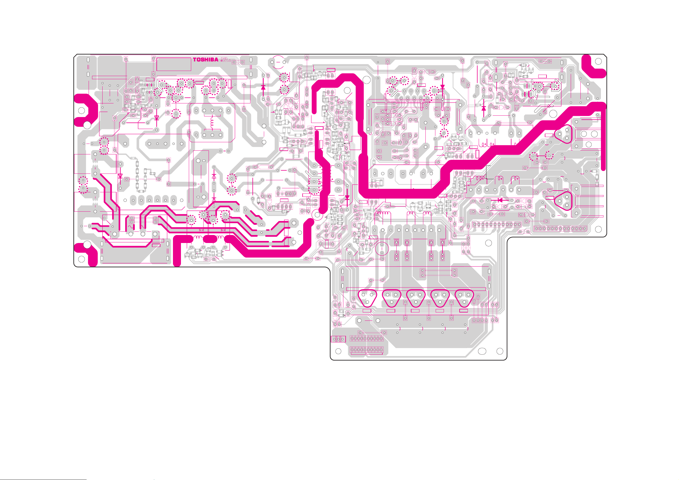
L8212
Q820A
PP83
C825
L821
GAP12
L820
GAP11
C824
PP84
R823
C8213
R8216
R8215
R820
C8240
+
D820A
R8214
D828
R8210
L8211
R821
D8274
R8218
D8273
D823
R8218
9
8
K
C8241
A
R8216
R8215
D8271
R826
R8249
R8249
C8240
R8246
R8245
POWER BOARD PD2171A1 (U002A)
BOTTOM (FOIL) SIDE
R8395
C8390
R8390
Q8390
D825
C8212
C8212
+
R8213
C8211
K
C8213
R8214
R8212
R8210
R8212
R8248
R8247
R8247
R8246R8248
R8245
R8244
7
R8213
A
C8211
R8241
R8241
R8242
R8243
R8244
Q820
6
C8210
C8210
T820
R8242
R8243
D8272
R8240
R8240
3
K
C8250
A
D824
LIVE AREA
1
2
C8251
1412
CAUTION
L825
16
1
KA
L823
C826
23547832
A
D822
C827
6
5
R825
L8242
SR80
T822
D842
D841
SR81
IS-P C3AE-568
L824
K
2
L8241
D821
C822
10
C840
+
R831
R841
F820
F2AL 250V
D826
C820
+
D845
D8403
D8403
C8403
+
R8118
R830
R8116
R8117
R812
R842
D843
C8401
C8401
D8230
R8118
R8117
R8217
C821
R812
C812
4
+
C812
R8130
D8231
D811
R8116
Q822
C843
Q840
D8404
Q812
R8130
D8230
R8217
R8412
R8411
R840
D8404
21
Q812
R8115
D8390
R8131
R8131
E
D8231
85
1
R8114
R8412
P802B
R8113
D8391
R8132
C845
C844
+
R8392
R8112
R8132
R8230
R8393
R8392
R8133
R8133
B
R8230
T840
Q841
D844
-
R8310
D8310
D8311
R8310
Q8311
D8310
Q8311
R8312
Q8312
R8312
Q8312
R8313
D8312
R8313
D8313
D8312
D8313
D820
Q8310
D8311
Q8310
R8391
R8394
R8394
R8393
R8110
R8111
+
4
1
R8390
R8161
C8490
C8390
R8395
R8162
R8160
Q813
PP85
C847
R8195
C8171
+
Q8390
R8194
D816
C817
R8141
R8396
Q816
C814
Q821
A
K
R
R8391
R8396
R8195
C8171
D8402
R8231
R8232
Q842
Q8391
R8194
D816
Q816
R8162
R8160
R8161
R8231
Q8230
D8401
D8402
R8410
C817
Q815
D819
R8141
R8144
R8232
6
D8401
R8410
C8402
Q815
Q8230
6
R8406
C8402
Q814
R8405
R8193
R8193
C814
R8143
D8232
R8403
R8403
R8404
R8409
R8407
L840
Q8191
R8140
R8142
C848
+
Q8191
R8150
Q8231
C846
R8408
R8151
R8409
R8408
R8407
C876
R8191
C816
+
C815
D8232
R8192
C819
C8191
C8191
R8191
R8152
R8233
Q8231
C816
R8152
R8151
D815
R8144
R8233
D846
D8701
C877
R8192
+
C818
Q814
R8142
R8143
R8405
R8406
+
R8704
R8704
R8140
R8404
R8709
R8709
R8150
Q862
D8702
D8702
D8701
+
R8701
R8705
R8705
R8701
C8702
R8710
A
R8708
K
R
R8703
R8702
R8702
R8605
R8707
R8708
R8703
R863
R8706
Q870
PP82
C862
R8605
C861
C860
L860
1
5
3
D860
D864
R8602
D862
+
C864
C863
R862
C8601
R864
R860
R863
1
C8605
C8605
R8706
R8707
C8702
R8710
17
D861
R866
C8602
Q8702
Q8702
R865
R8716
Q860
R8601
C869
C868
T860
R8716
Q8703
Q8703
D863
Q8704
R867
11
C870
12
C865
D8602
75
Q8704
14
R8603
C8703
R8711
D866
C866
Q864
R8604
R8711
15
R8606
Q8701
C8703
R8712
D8601
Q882
Q8701
R8811
R8812
R8813
R8712
E
D865
D8602
R8809
A
R8811
R8813
R8603
L862
Q860A
R8606
R8604
R8713
R8714
R8809
R8812
Q8601
R8713
R8714
K
Q8601
D8601
R8810
C8801
R
C898
Q8602
+
Q8602
B
R8806
R8807
D8801
D8802
C892
+
C8701
F2AL 250V
F870
L872
13
L870
L871
9
L873
R8607
1
R8607
Q863
R8808
16
12
R880
R881
C891
C893
POWER
R8802
R8802
Q881
C8891
C884
+
D880
2
POWER_SIG
PROTECT
C885
+
ACDETECT
R8807
R8810
D8801
D8802
C8801
P809B
GND
D883
R8806
R8804
4
R8808
5V-1
R8804
24V
R8803
D881
R885
T880
D885
GND
D888
C883
D882
S-GND
C8802
C8802
C886
R8801
R8801
6
R886
D891
S-GND
30V
D887
R8814
7
30V
D8805
R8814
7
D892
D889
D890
D8805
Q8801
Q8802
Q8801
Q8802
R8815
R8815
6
1
4
C882
3
Q880
C881
L886
C880
Q880A
R882
R884
R883
C899
PP81
D884A
+
D884
C888
+
C890
12V
L881
D8803
+
D8804
D8803
D8804
R8805
R8805
1
12V
L880
10
C887
C894
C897
C896
D886
C889
+
C895
+
D886A
L883
+
L884
1
13
20V
P807B
GND
GND
GND
GND
GND
12V
20V
20V
12V
32V
D8705
PG03
R8715
R8715
D8706
D870A
C878
D8706
10
10
GND 24V INV
D874
L878
C874
D873
+
+
C875
D872
D870
D871
++
C872
1
P860
C873
1
P861
– 29 – – 30 –
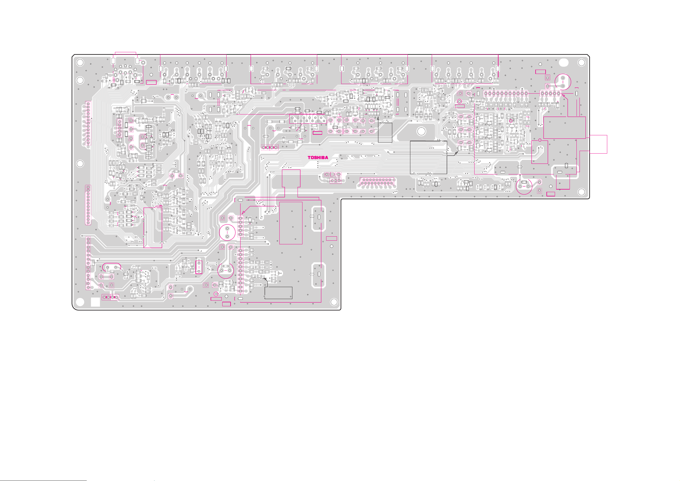
TN AV BOARD PD2235B1 (U003A)
BOTTOM (FOIL) SIDE
SW_E3
SC_E3
SY_E3
AUDIO-GND
AUDIO-GND
ACDETECT
RS530
C1802
C1802
P516B
EXT5
RV244
RV244
RV241
GC02
Q620
QS108
Q620
RS530
QS108
R620
RS529
R621
RS529
C652
C652
C677
Q671
R670
R670
QS05
R620
R621
C651
R676
R677
C651
R677
R676
Q671
C678
C678
R673
R673
C687
R681
R681
C688
R-1786
DE99
13
PJ21A
9V1
5V-2
GND
PV04
RV245
L
Y
CC66
RS25
GC02
RS25
RV241
RC03
CC66
RC03
CS39
D617
D617
D619
RS35
CS12
D619
CS12
QS05
RS35
RS18
D614
Q672
D618
D615
D614
R672
Q672
R672
R664
C661
R665
R680
R680
+
C665
+
C666
9: V_PC
8:H_PC
7:GND
6:B_PC
5:GND
4:G_PC
3: GND
1:GND
2:R_PC
2
1
RV245
RV242
CS39
DS13
D613
10:GND
C662
11:L_PC
RV246
R
Cb
RV246
RC04
RS90
RS73
RS74
RS63
16:GND
RC04
QS14
RS74
18:R_HDMI2
17:L_HDMI2
18
19
Q610A
19:GND
Cr
RV243
RV243
RS04
RS04
CS04
CS06
CS04
CT14
RT27
RT26
QT09
RT08
RT09
QT03
CT02
CT08
RT18
QT06
RT17
C1805
C1805
RS26
CC67
RS26
CC67
RV242
Q627
Q627
RS90
RS73
RS91
RS63
QS14
QS18
QS18
RS91
RS18
DS13
D618
D615
D613
R664
C661
R665
C662
15:R_HDMI1
14:L_HDMI1
13:GND
12:R_PC
PV99B
MONI,AUDIO,WOOFER
V
GJ603
CC21
R229
LC13
CC21
LC13
R229
GJ603
RS16
RS09
RS08
RS16
RS12
QS04
RS12
RS08
RS09
RS07
RS06
RS06
CS06
QS04
RS19
RS10
RS07
RS19
RS17
RS78
RS10
RS17
RS78
RS05
RS81
RS05
RS03
RS03
QS03
RS81
QS03
RS20
RS20
CS05
CS03
CT18
CS05
CS03
CT12
CT12
RT23 RT22
RT21
QT08
GT03
RT19
QT07
RT24
RT20
RT04
RT05
RT03
QT02
GT01
RT01
RT06
QT01
RT02
RT14
RT13
QT05
RT12
GT02
RT15
RT10
QT04
RT11
C1806
C1810
C1809
C1811
C1811
C1807
C1808
C1806
C1810
C1809
C1808
C1807
PV05
LW
CC76
CC74
GC04
LC09
GC05
LC09
CC74
GC04
GC05
C119
+
PK02
R115
TP-12
CT18
LT0 3
RT27
QT09
LT0 1
CT06
CT06
QT03
RT09
RT08
CT02
LT0 2
RT18
QT06
GR05
GR05
C117
C117
C118
GR06
GR07
GR06
C118
GR07
R
CC75
LC11
LC11
LC10
LC12
CC75
LC10
CC71
CC76
CC71
LC12
17
P515B
C102
+
7
6
L101
3
2
R111
R112
R115
R111
Q102
R114
R112
R113
Q102
R114
R113
RT23
GT03
CT14
RT24
RT26
RT05
GT01
QT02 QT08
QT01
RT06
RT14
GT02
QT05
CT08
RT17
QT04
RT15
GR08
GR26
GR25
GR08
GR26
GR25
L190
R167
C116
C103
QT07
C115
C1803
C114
C116
C114
C113
C115
L190
C190
R169
C161
CT13
R161
R166
B
CT13
Q161
R165
C163
CT01
R162
C164
R168
CT01
R163
Q162
CT07
R170
R164
Q162
C162
R170
CT07
C162
R164
GR612
GR612
C1804
C1803
C1804
GR28
GR28
C103
R167
RT22
RT21
RT19
RT20
RT04
RT03
RT01
RT02
RT13
RT12
RT10
RT11
GR27
GR27
C111
R102
R101
C113
C112
C112
L103
L102
L103
C190
L102
R103
R108
R108
R107
R107
Q101
Q101
R105
R169
R104
R105
R161
R104
C163
R162
GR101
GR101
L110
C101
C111
C110
D101
D101
C110
R101
C101
R102
13:AUDIO det out
14:SIF out
15:32V
16:NC
17:VIDEO out
B
C161
R166
R103
Q161
R165
R163
R168
C164
12:AFT
9:NC
10:SCL
11:SDA
GR614
2:NC
3:5V
4:NC
5:SW1
6:SW2
7:VT
8:RF AGC
H001
GR614
+
C105
PK01
CV59
PV02A
PV02B
V
RV248
RV248
R645
R645
R644
R644
GRV28
GRV28
LV1 5
L
CC79
RC16
RS97
GC03
RC38
CC70
GC06
CC79
RC16
RS97
GC03
RC38
GC06
CC70
C612
CS40
CS40
RS40
GR623
GR623
GR624
GR624
CS78
RS52
CV33
RV45
RV47
QV06
CY03
RY06
RY09
QY03
CY02
QY02
RY05
RY08
CY01
QY01
RY04
RY07
RY07
RY11
RY11
CV42
QV05
RV60
RV66
RV66
R
CC82
RC13
RS96
RC05
RS96
RC13
CC82
RC05
+
GR621
GR622
GR621
GR622
CS41
CS41
CS42
CS43
RS40
RS41
RS43
RS42
RS41
RS43
RS42
GR628
GR627
GR628
GR627
RS68
CS79
CS78
CS79
RS68
RS52
RS53
RS53
CS52
CS53
CS53
CS52
RC37
CC69
RC06
RC37
CC69
RC06
C653
C653
R652
D612
R652
D612
R655
Q612
Q612
R667
R655
R667
R6605
R650
Q665
R6606
R650
CS46
CS47
R6605
Q665
R6606
CS48
CS46
CS47
CS43
CS48
CS49
CS49
CS42
RS47
RS46
RS49
RS48
RS49
RS46
RS47
RS48
RS51
RS85
RS85
RS86
RS50
RS86
RS51
RS50
CS86
CS86
CS85
RS67
CS51
CS50
CS85
RS67
CS51
CS50
CY102
+
23
LY1 0 1
6
+
7
CY105
C4407
R4430
R4474
R4430
C4407
C4408
R4473
R4474
R4473
C4409
C4408
X4010
R4408
R4408
+
CY119
GR151
GR151
LY1 1 0
QY102
RY115
+
RY115
QY102
RY112
RY111
RY112
PK04
TP-12A
RY111
RY113
RY114
RY113
RY114
EXT4
RV240
RV240
RV231
RV231
Q622
Q621
R654
Q622
Q621
R651
R654
Q664
Q664
+
R651
R653
R6603
R653
R6603
C680
C601
C601
4
PV03
RV237
R
Cb
RV236
RS24
RV232
RS24
C690
C690
D607
11
D675
D640
RV237
CC63
RC02
RC02
CC63
C632
C632
D674
D640
D641
D641
+
C681
R684
R684
23547871
Cr
RV233
RV233
C655
Q615
Q615
C655
R617
R617
C677
R675
R671
R675
R671
2
+
1
R697
R697
C671
+
Q610
C674
RV236
L
Y
GC01
RC01
RS23
RC01
GC01
CC62
RV232
RS23
CC62
D607
12
R685
C696
R685
C696
P601
GND
R-AUDIO
D674
+
D675
C682
C602
C602
C694
C694
1
GND
L-AUDIO
HY01
2:NC
3:5V
4:NC
RY108
RY108
RY107
RY103
CY114
CY115 LY102
LY190
CY116
RY104
RY105
5:SW1
6:SW2
7:VT
8:RF AGC
9:NC
10:SCL
11:SDA
12:AFT
13:AUDIO det out
14:SIF out
15:32V
16:NC
17:VIDEO out
QY101
QY101
RY104
RY105
LY1 0 3
RY107
RY103
CY190
RY106
GR158
GR157
GR158
GR157
DY10 1
CY101
DY101
CY101
RY102
RY102
CY110
CY110
CY111
CY111
RY101
RY101
CY112
CY112
CY113
CY113
LY10 3CY114
LY10 2
CY115
CY190
LY19 0
CY116
RY106
CY120
CY120
LY104
LY10 4
CY103
CY103
17
PK03
PV01A
CV08
CV08
RV234
RV234
13
9V1
RX_BM
TX_BM
GND
R_BM
P602A
GND
L_BM
PM02
GND
R_HP
CR_BM
GND
CB_BM
GND
Y_BM
1
RV14
CV21
12
GND
GND
R_E3
L_E3
GND
V_E3
GND
GND
GND
+
CV63
PV25A
RV03
RV01
RV06
1
1
26V
26V
P803B
5V1
32V
9V-1
C1801
GND
GND
C1801
5V-3
5V-3
L505
GND
13
C514
PM01B
4
GND
DET_HP
L_HP
GND
DV12
RV03
RV01
RV06
RV04
RV04
GND
RV212
RV235
RV211
RV14
CV21
CV07
RV212
RV211
CV07
C656
R646
Q668
Q668
R646
C656
C633
C649
C633
R629
R629
5
GND
R631
R631
R632
R632
1
R630
R630
C634
C634
C650
Q669
Q669
Q674
C646
R647
R647
C646
Q674
RV15
RV16
R628
CV23
RV16
R628
RV15
DV24
DV24
CV23
CV22
DV12
DV13
CV22
DV13
RS94
RS95
CV20
CV20
RS94
RS95
CV19
RV12
CV19
CV74
CV74
RV29
RV29
CV13
CV12
DV06
CV13
DV01
CV12
DV11
CV11
DV04
CV09
DV04
CV09
CV11
P517B
RV235
GRV30
GRV30
LV10
LV10
C658
R627
Q673
R627
Q673
C658
R626
+
R625
D691
+
D694
C641
D693
+
D690
R649
C659
C659
R648
R648
CV24
DV15
DV15
CV24
DV16
DV16
CV25
DV17
CV26
DV17
RV13
RV13
RV12
RV53
RV53
RV74
RV74
RV28
RV28
DV06
RV43
GRV74
DV01
RY03
DV11
RY02
RY01
RV52
X501
C516
C516
+
1
5V-3
5V-3
R518
R519
R518
R519
R501
R501
C524
L504
C524
L504
L502
L502
R504
R505
C507
C509
C508
C507
C509
C508
EXT1 & EXT2
RV247
RV247
+
R656
R656
QS06
C657
QS06
R657
R626
D694
QV06
GRY73
GRY72
GRY71
GRV73
C502
R657
C657
R625
C645
C648
D691
C648
C645
D692
D692
C644
C647
D693
C647
C644
D690
R649
CV25
RV17
RV17
RV18
RV18
RV19
RV19
CV26
RV41
RV41
CV01
RV40
RV40
+
RV56
RV56
RV43
GRV74
RY03
GRY73
RY02
GRY72
RV47
CV33
RV45
RY01
RY06
QY03
CY03
RY09
GRY71
RY05
CY02
RY08
QY02
RV52
GRV73
RY04
CY01
QY01
CV42
RV60
QV05
C502
R504
R505
L400
– 31 – – 32 –
 Loading...