Toshiba 20AF45, 20AF45C Schematic
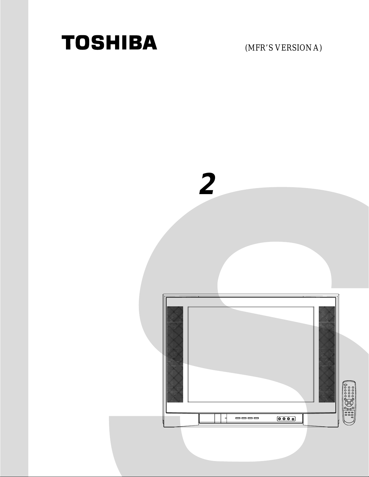
FILE NO. 053-200504A
SUPPLEMENT
This Supplement serves as an update to the original 20AF45C Service Manual, file number 050-200504.
Please refer to this Supplement in conjunction with the original Service Manual when servicing this
model.
(MFR’S VERSION A)
SERVICE MANUAL
COLOR TELEVISION
2
20AF45C
DOCUMENT CREATED IN JAPAN, August, 2005

SERVICE INSTRUCTION
Product: COLOR TELEVISION
ORION ELECTRIC CO.,LTD.
41-1 IEHISA-CHO,TAKEFU-CITY,FUKUI 915-8555 JAPAN
FACSIMILE: (0778)24-5456 PHONE: (0778)23-0001
FILE NO. 053-200504A
DATE:Aug.,2005
RANK:
A
Model: 20AF45C
Corrective reason:
Corrective action:
Applicable units:
Performance improvement of PCB
Parts exchange.
BA302015904 or younger.
ORION ELECTRIC CO.,LTD.
NOBUO TSUKAMOTO
MANAGER
TEC-HQ 2TEC SEC3
TECHNICAL ENGINEERING DEPT
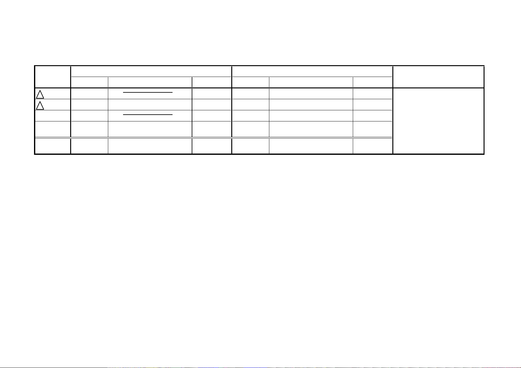
ELECTRICAL REPLACEMENT PARTS LIST
MFR'S VERSION A MFR'S VERSION B
REF. NO.
! R517 R3X28BR22J R,METAL OXIDE 0.22 OHM 3W AD301973 PCB VERSION UP.
! R518 R3X28BR22J R,METAL OXIDE 0.22 OHM 3W AD301973 DELETE
C625 CS0PB0415K CC 0.1 UF 50V B AE005068
PCB010 A3S002U010
PART NO. DESCRIPTION TSB P/N PART NO. DESCRIPTION TSB P/N CAUSE
MAIN PCB ASS'Y (VERSION A)
CME017A
AE006897 A3S002U010
MAIN PCB ASS'Y (VERSION B)
CME017B
AE006897
PCB110 A3S002U110
All parts are not interchangeable between version.
CRT PCB ASS'Y (VERSION A)
CCE011A
AE006219 A3S002U110
CRT PCB ASS'Y (VERSION B)
CCE011B
AE006219
W179
CP1001
C1011
J1001
W133
W138
S801Y
C1532
R1515
C1514
L1504
C1515
R1507
W848
W178
C1501
R1516
W177
R1012
W859
W018
L1501
W057
W145
C1503
B1502
C1512
C1521
W015
W858
W146
R1503
W162
W016
TU001
W137
W014
C641
L1503
W837
C1513_1
R1013
D001
C1006
W011
R649
W147
W142
W143
C1504_1
W865
R1511
C626
W165
W079
R304
R303
C316
C618
C1009
W066
W164
W058
R601
W172
C001_1
C1005
IC1001
R602
W140
W020
R614
CD802A
W078
C314
C1012
D709
R1015
HS1001
C319
C733
R1014
W152
W154
W144
W160
Q606
L1507
C602
D604
CP802A
C317
C308
W812
R1002
W005
W151
Q604
C603
Q601
R623
W115
L301
J702
W135
S803X
C514_1
W008
W155
R603
C608_2
C609
Q611
W167
C305
R301
W134
W017
W139
C304
C725
W819
W820
S802X
S802Y
C615
W170
C633
C333
C302C306
Q602
C606
W169
W096
R302
W180
D704
C621
W862
R1010
R1016
R616
D601
S801X
W110
R626
W095
C722
W006
Q607
D605
W176
D703
W174
W175
J701
C614
C619
D602
C629
W092
J705J706J707
C605
C610
D606
W833W832
C903
W077
W076
W073
W059
R1001
W187
C622
S804Y
D706
D701
W075
C611
C904
W072
W087
W102
W100
J704
R517
W069
X602
W831
W109
W090
R617
W089
W021
W104
C905
W074
W070
W068
C630
D607
W829
W830
D702
C642
S804X
W113
W098
C907
W105
W125
C916
C910
W067
C919
C914
W185
C645
W081
C638
W012
W111
L901
W065
D608
TP005
W086
R612
W046
W045
W114
W093
D105
W844
R407
W022
W025
W112
W129
R119
CP101
R441
R436
TP006
D415
C408
W024
W048
W107
W108
W106
D104
W091
CME017B
W128
R139
R140
W118
W121
W116
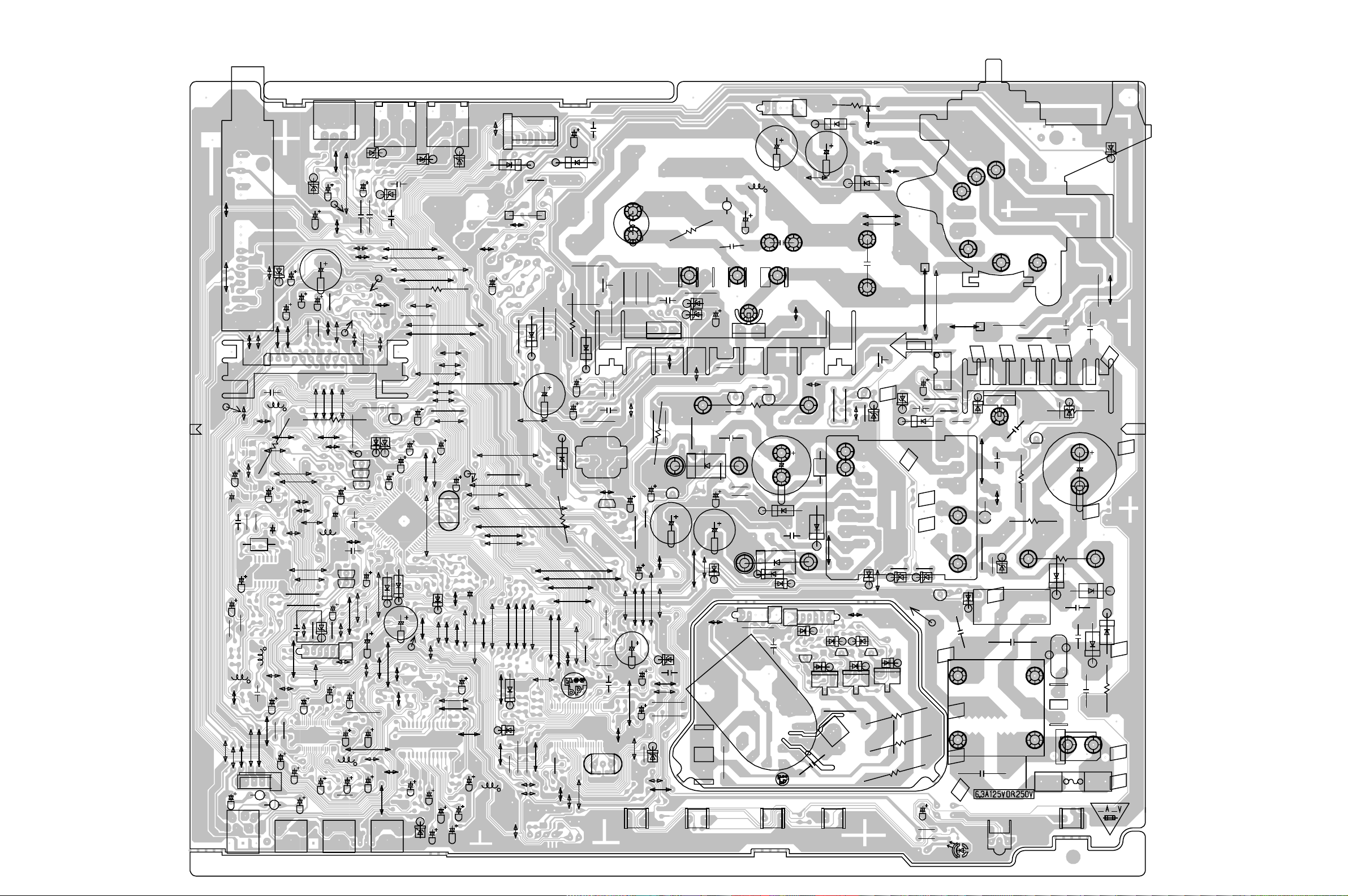
PRINTED CIRCUIT BOARDS
MAIN/CRT (INSERTED PARTS)
SOLDER SIDE
(MFR'S VERSION B)
D411
C407
W094
R418
D402
W041
W120
R422
W097
W052
VR401_1
R406
T401_1
Q402
R124
R453
X101_1
C427_1
L402_1
R439
R421
R429
R433
C417_1
C402
W027
R130
R413
R132
W053
R427
R414
C113
IC401
W871
R002
R
527
C539_1
W037
R146
R537
W032
C110
W049
W035
W056
W055
W050
Q512
C527
W039
W033
D406
C109
R133
R515
D106
C403
R426
C139
W040
C122
W028
C114
W822
SW103 SW104 SW101
W019
R001
D403
R535
W806
R536
C504
R437
W821
R503
D410
C501
W043
CP801B
W054
R402
C410
C425_1
CP401
C409
R428
Q503
R505
C517_1
D510
R524
R546
D513
CD801B
R804
CP803
CCE011B
L401
R420
R
D414
4
5
2
_
1
W103
W123
R416
W030
W071
R118
C430
R410_1
C406
W044
W805
R507
D517
R824
CD801A
Q505
R434
CP801A
C413_1
C418
Q405
HS402
C521_1
D511
C520
D505
D514
C801
R438_1
D407
W001
W853
W863
R553
D512
CP802B
CD802B
D810
D811
Q801
Q803
D802
J
8
01
_1
C802
SW102
B504
W825
Q805
R554
R806
C426
C420_1
Q507
W817
W802
D812
D801
CP806
W007
D405
R506
D520
Q804
W857
VR502
W850
D528
W861
W813
T501
W013
Q802
D509
R510
D508
Q806
R802
R
R805
D803
8
TP004
C509
D506
07
803
R
C108
W010
R547
D525
Q504
R120
R102
C524
W009
S803Y
D109
R543
W003
IC504
R508
R545
D516
C
519_1
TP003
D524
Q502
C505_1
FB401
W004
B501
R539
R540
L501
OS101
R430
C535_1
C512
W801
C506_1
R502
D523
R432
Q514
RY501
R520
R541_1
CP508
D503
FH502
C415_1
R544
D507
C507
R501
CP507
TH501_2
F501
SW105
C508_1
R542
D502
C503_1
C502_1
CP502
CP501
R443
HS501
C513_1
FH501
D404
W002
ATTENTION
D501
D504
R500
CAUTION
FOR SERVICE INFORMATION ABOUT CRITICAL
COMPONENTS, SEE INSIDE BACK COVER.
INFORMATION POUR SERVICE DES
PIECE CRITIQUE, VOIR AU VERSO.
RISK OF FIRE
- REPLACE AS MARKED.
R517
ADD:
W139
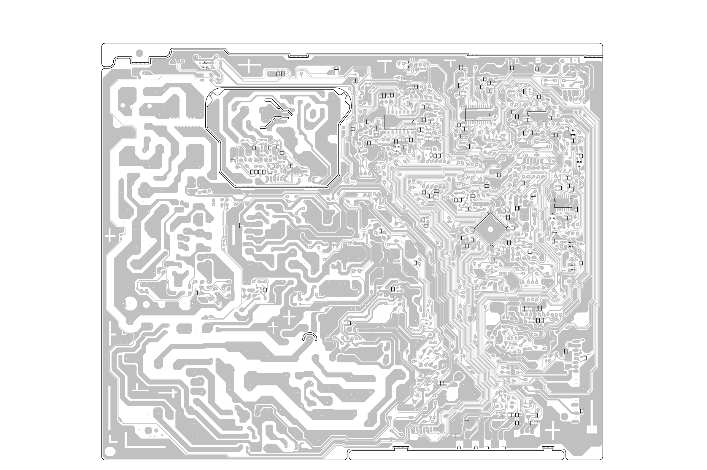
PRINTED CIRCUIT BOARDS
MAIN/CRT (CHIP MOUNTED PARTS)
SOLDER SIDE
(MFR'S VERSION B)
Q101
R532 R533
R810
R801
C511
R813
R811
R815
R809
C811
C809
R808
R821
R819
R818
R817
R812
R103
C810
R814
R106
R820
CCE011B
R816
C805_1
R109
R525
R114
R101
R113
R112
R131
C106
C115
R138
R137
C119
C121
R125
C117
C111
R409_1
C102
C104
IC101
CME017B
R122
C146
C131
C145
C125
Q103
R403
IC199_1
R105
C120
R150
R110
R126
C143
R401
R134
R128
C128
C141
R127
R628
R627
R136
C644
C140
W811
R142 R129
R141
C643
C136
R145
C637
R135
R143
C137
C135
C138
R632
R629
C912
C911
R625
C908
C918
C917
C913
C632
C915
R912
R634
R618
R652
R653
R622
C631
R746
C607
C142
R636
C628
1
R610
R654
C616
C640
C741
C303
R314
C301
R620
R611
R609
C612
R724
R745
C720
C719
R907
IC902
R635
R641
17
33
IC601
49
R651
R621
C334
C309
C307
C625
R1514
C311
IC302
C310
R1502
C313
C742
C312
C315
C322
C320
Q1501
Q1507
C1505
C1507
R1517
R1505
C1502
IC1501
R1509
R1518
C1517
C1519
C1510
C1509
R1510
Q1502
R1513
C1522
R1504
R1506
C1516
C1518
C1508
IC1503
IC1502
R1508
C1526_1
Q1505
C1511
C1523
C541
C554
R513
R516
C405
R417
C416
R415
R404
C439
C411
R730
R725
C624
R736
R726
C736
R729
R733
C738
C1007
R1017
C1004
R1008
C1003
C734
C1002
R1006
R739
R735
R1003
C1001
C005
R006
C002
ADD: C625
8
ADD: C625
7
6
5
4
3
2
ABC D E F GH
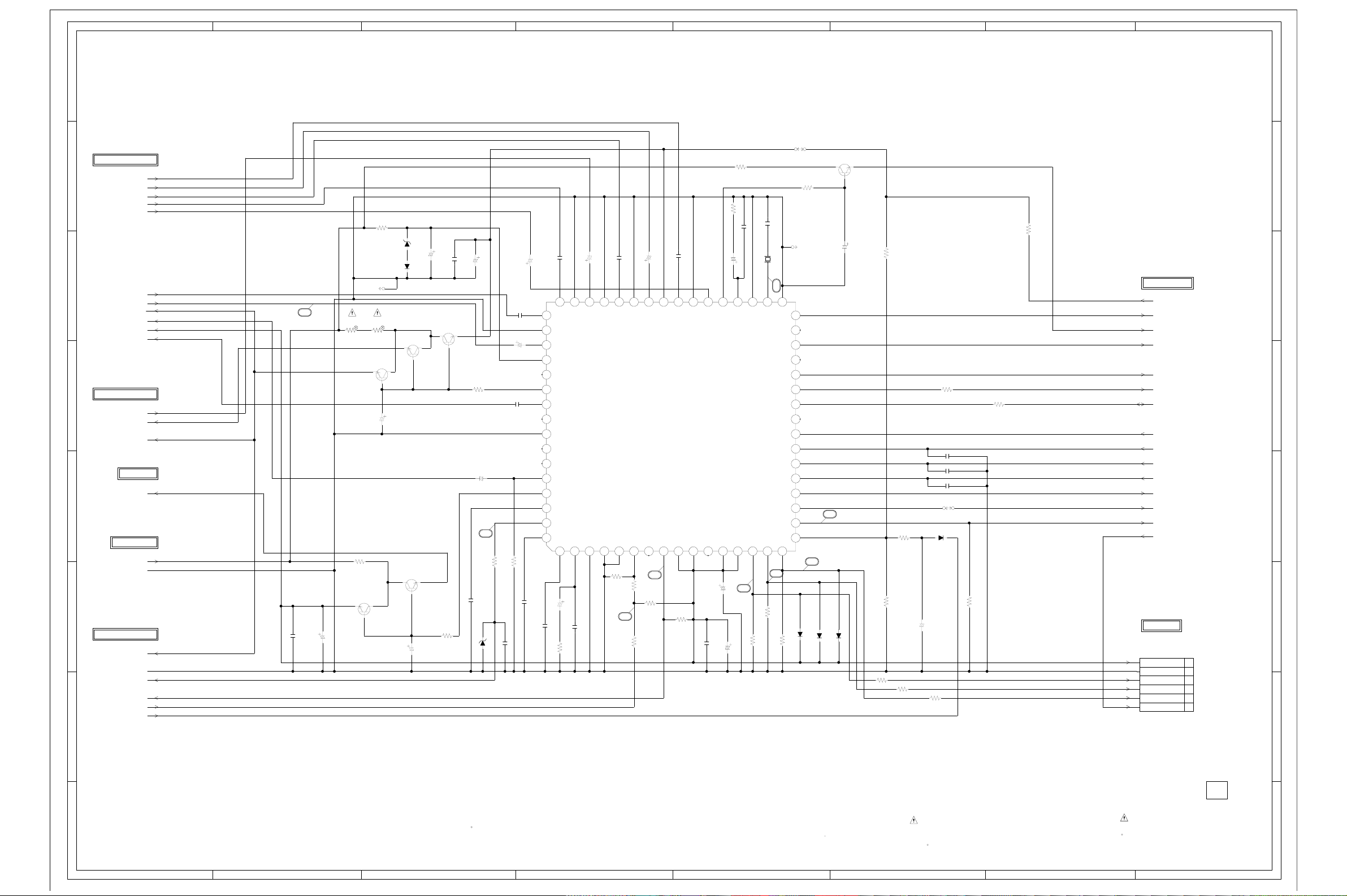
CHROMA SCHEMATIC DIAGRAM
(MAIN PCB)
(MFR’S VERSION B)
W831
FROM/TO COMB FILTER
V_IN[YUV]
VIDEO_IN1
U_IN[YUV]
Y_IN[YUV]
VIDEO_IN3
C_V_OUT_SW
Y_V_OUT_SW
P.CON+5V
VIDEO_OUT
P.CON+8V[A] AT+5V
FSC_OUT
FROM/TO TUNER/STEREO
TUNER_VIDEO
TUNER+5V
P.CON+5V
TO SOUND
P.CON+8V[B] VD
FROM POWER
UNREG+12V
GND
FROM/TO DEFLECTION
P.CON+5V
GND
V_OUT
H.OUT
H_SYNC
ABCL
C625
7
P.CON 5V REG
KTC3209_Y
10016V YK
C645
0.1 B
R602
12 3W
Q602
R601
15 1/2W
P.CON 8V REG
Q601
KTC3209_Y
7.9
R603
330 1/2W
S801X
R649
10 3W
5.0
C603
11.3
8.5
7.2
5.5
4716V YK
D602
MTZJ8.2B
D601
1SS133
7.2
5.0
5.5
P.CON 5V REG
Q604
KTC3209_Y
P.CON 8V REG
Q611
KTC3209_Y
7.911.3
8.5
4716V YK
C602
4716V YK
C605
P.CON+5V REG
Q606
KTC3209_Y
7.2 5.0
R609
100
C607
5.5
0.01 B
C610
C608_2
C606
4716V YK
R610
100
1016V KANP
8
0.33 TF
D604
R614
C626
MTZJ12B
2.2K 1/4W
C641
0.1 B
C642
C640
0.01 F
R621
0.0047 B
9
150V KA
V/C VCC
H OUT
C624
V IN(YUV)
CHROMA IC
IC601
M61283BFP
NC(Vcc)
R636
1.5K
B
0.1
NC(GND)
DEF VCCNCNC(Vcc)
KA
150V KA
C614
C611
2.2
C IN(Y/C)
49
0
NC(GND)
50515253545556575859
3.0
150V KA
C609
Y IN(Y/C)
8.7
VREG VCC
1.9
CVBS4
NC
5.7
5.7V VREG OUT
3.2
fsc OUT
0
NC
NC
0
FAST YUV
2.8
DELAYDE Y OUT
NC
3.0
EW OUT
NC
3.0
VIDEO LINE OUT
6061626364
8.7
8.7 VREG OUT
4.0
VRAMP AGC CAP
4.0
V OUT
4.0
VRAMP CAP
110
3.2 4.0 0 0 0 5.5 0 3.8 8.0 8.0 0 8.0 8.0 4.0 4.0 4.0
2.2K
C615
0.1 TF
C612
0.01 B
R611
150V
C619
C618
0.1 B
CVBS1
NC(GND)
HVCO F/BDEF GND1
LOGIC GND
2
3
150V KA
C616
0.01 B
6.8K
U IN(YUV)
47 NC(GND)
48 Y IN(YUV)
1 HVCO F/B
DEF GND2
5
R654
56K
10
0.1 B
R641
R612
C621
NC(GND)
FBP IN
6
10K
10K 1/4W
CVBS2
NC
789
NC
R635
120K
R616
120 1/2W
8.2K
R618
B
C632
C631
0.015
0.4750V KA
X602
C630
CVBS3
MCU 5.7 VREG OUT
33 V/C GND
34 XTAL 3.58
15 G OUT
16 B OUT2 AFC FILTER
11 12 13 14 15 16
NC
C633
C628
C629
0.01 B
10050V YK
100016V YK
C_APC
NC(GND)
MCU CLOCK OUT
V PULSE OUT
INV.FBP OUT
MONITOR OUT
HI VCC
R OUT
13
R651
100DT3R531
Y SW OUT
MCU RESET
P_CON CONT
CLK CONT
FAST BLK
R652
3.3K
18P CH
S804Y
3.579545MHz
12
03.202.85.61.901.25.01.901.203.002.7
333435363738394404142434445464748
NC
SCL
SDA
R IN
G IN
B IN
ACL
14
3.3K
3.3K
R653
R617
100 1/4W
3.6
0
NC
5.0
30 31 32
3.5
NC
5.0
3.5
3.5
4.9
NC
4.2
2.9
2.9
2.9
4.6
20 21 22 23 24 25 26 27 28 29
4.9
4.9
2.1
17 18 19
15
1SS133
D605
D606
5.5
11
D607
1SS133
C622
1SS133
4.98.8
AT+5V REG
Q607
KTC3203_Y
4716V YK
R620
100
R622
R625
6.8K
R629
6.8K
5.6K
R623
100 1/4W
C637 33P CH
C643 33P CH
C644 33P CH
11E1-EIC
1016V KANP
C638
R626
100 1/4W
D608
R627
100
W805
R632
1K
R634
R628
100
33K
FROM/TO MICON
PROTECT
SW_Y_OUT
RESET
POWER
SCL
SDA
OSD_BLK
OSD_R
OSD_G
OSD_B
HD
SYNC_OUT
CLAMP_OFF
TO CRT/SVM
(CP802B)
CP802A
B2013H02-6P
P.CON+8V
GND
R.OUT
G.OUT
B.OUT
CLAMP_OFF
8
7
6
5
4
3
1
2
3
4
5
6
2
PCB010
CME017
NOTE:THIS SCHEMATIC DIAGRAM IS THE LATEST AT THE TIME
1
OF PRINTING AND SUBJECT TO CHANGE WITHOUT NOTICE
NOTE:THE DC VOLTAGE AT EACH PART WAS MEASURED
WITH THE DIGITAL TESTER WHEN THE COLOR BROADCAST
WAS RECEIVED IN GOOD CONDITION AND PICTURE IS NORMAL.
ATTENTION
:LES PIECES REPAREES PAR UN ETANT
DANGEREUSES AN POINT DE VUE SECURITE
N’UTILISER QUE CELLS DECRITES
DANS LA NOMENCLATURE DES PIECES
CAUTION
:SINCE THESE PARTS MARKED BY
CRITICAL FOR SAFETY,USE ONES
DESCRIBED IN PARTS LIST ONLY
ARE
1
ABC D E F GH
ABC D E F GH
ADD: R517
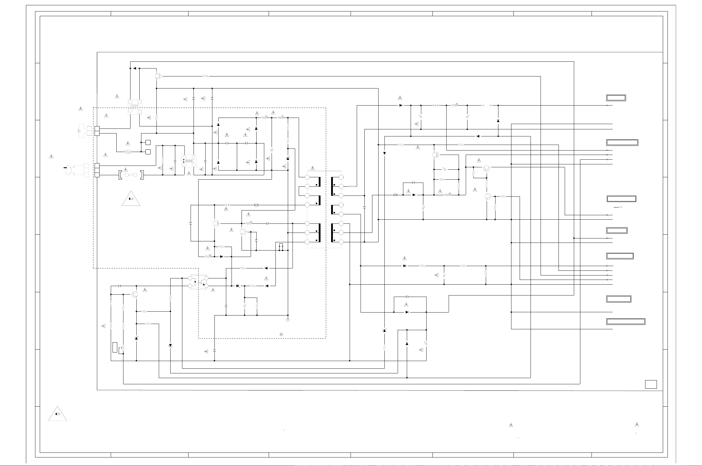
POWER SCHEMATIC DIAGRAM
8
(MAIN PCB)
(MFR’S VERSION B)
8
7
6
5
4
3
AC120V_60Hz
CD501_1
09615904
WIDE
BLADE
DEGAUSS COIL
L503
8R200024
WHITE
BLACK
21
21
1
2
G5PA-1-SA(WEC)
CP502
A1561WV2-2P
CP501
A3963WV2-3PD
WHITE
12
BLACK
W817
R506
RY501
TH501_2
B59203-S1060-B14
F501
6.3A125V
FH501
EYF-52BCY
6.3A125Vor51MS063L
6.3A 125V
C554
0.022 B
6.3
R553
6.8K 1/2W
1/4W
R554
100K 1/2W
6.8K
VR502
+B ADJ
D516
1SS133
3
9.7
5.7
22K
12
4
FH502
EYF-52BCY
D528
CP507
003P-2100
1
1
CP508
003P-2100
FEED BACK
SWITCHING
Q507
KTC3198
R532
1.5K
R510
100 1/4W
MTZJ5.6B
10.9
RELAY DRIVE
0
R500
KTC3198
0
2.7M 1/2W
R520
Q504
+-10%
1.5M 1/2W
D508
C505_1
COIL,LINE FILTER
R533
270
MTZJ3.9B
1R5A123F28Y
10K 1/4W
0.0015250V KX
C513_1
34
0.22275V ECQUL
12
L501
0.00222KV RR
C535_1
0.15
10.7 16.3
1
9.7
2
R515
C519_1
0.1275V ECQUL
C506_1
159.4
R542
1W
1.5
34
FEED BACK
IC504
LTV-817M-VB
C508_1
D
0
S
0.0015250V KX
D501
RM11C-EIC
C502_1
D504
RM11C-EIC
SWITCHING
Q502
2SK3326(2)
G
5.3
R544
270 1/4W
D507
1SS133
0.0022250V KX
0.0012KV
W801
SWITCHING
Q514
KTC3203_Y
MTZJ18B
C541
0.056 B
2KV
RR
5.3
R545
150 1/4W
D509
C503_1
0.001
R502
330 2W
0
C509
1.5
100 1/4W
D502
RR
D503
B501
BL02RN1-R62
C524
R508
4725V YK
R543
R501
17W
RM11C-EIC
C507
RM11C-EIC
C512
0.047100V MMTS
0.001500V B
D524
1SS133
D506
1N4937
1K 1/4W
R541_1
0.22 1W
470200V UP
HS501
763WAAA074
GND1
D523
IS THE LIVE CONNECTIONCAUTION:
R539
R540
1/4W
1.2M
1/4W
1.2M
MTZJ18B
141.6
40.0
159.4
138.9
8
P1
7
0
6
P2
5
3
2
1
T501 8135091S
7
TO SOUND
SOUND+B
GND
SOUND_GND
FROM/TO DEFLECTION
H+B
+B
FBT+B
GND
TO TUNER/STEREO
S803Y
P.CON+B
GND
TO CHROMA
UNREG+12V
GND
FROM/TO MICON
P.FAIL
X-RAY
DEGAUSS_H
POWER
GND
FROM/TO SOUND
GND
FROM/TO COMB FILTER/AV
GND
6
5
4
3
220025V YK
Q505
S802X
D517
1SS133
115.5
10K
+B SW.
Q503
2SA1371
1/4W
R507
R525
S802Y
114.7
115.2
0
115.1
82K 1/4W
15K
0
R513
D513
1SS133
R516
10K
10K
D505
30PRA60-FC
C501
220025V YK
R503
10K 1/4W
B504
D511
1N4937
C520
0.001500V B
D512
21DQ09N
D520
CURRENT DET.
2SA1624
C517_1
0.00152KV RR
D510
FE201-6L49
1SS133
D514
1SS133
50.0
9
NC
25.0
W825
10
0
11
240.0
NC
12
13
0
14
26.0
15
16
C511
W5RH3.5X5X1.0
220P CH
D525
MTZJ12B
R547
100 1/4W
Q512
R546
100 1/4W
C521_1
C527
38
115.7
220160V ED
220016V YK
W806
115.4
R536
47K
C539_1
2.2100V YK
1/4W
R527
0.68 2W
C504
R517
0.22 3W
100K 1/4W
R535
3.3K
2.250V YK
R537
R524
C514_1
R505
3.9K 1/4W
STAND BY SW.
2SC2909
1/4W
2
6.3A 125V
CAUTION
1
ATTENTION
2
PCB010
CME017
:FOR CONTINUED PROTECTION AGAINST FIRE HAZARD,
REPLACE ONLY WITH THE SAME TYPE FUSE
:POUR UNE PROTECTION CONTINUE LES RISQUES D’INCEIE
N’UTILISER QUE DES FUSIBLE DE MEME TYPE
6.3A 125V(F501)
6.3A 125V(F501)
NOTE:THIS SCHEMATIC DIAGRAM IS THE LATEST AT THE TIME
OF PRINTING AND SUBJECT TO CHANGE WITHOUT NOTICE
NOTE:THE DC VOLTAGE AT EACH PART WAS MEASURED
WITH THE DIGITAL TESTER WHEN THE COLOR BROADCAST
WAS RECEIVED IN GOOD CONDITION AND PICTURE IS NORMAL.
THE RESISTOR MARKED F IS FUSE RESISTOR.NOTE:
THE ALUMI ELECTROLYTIC CAPACITOR MARKED NP
IS NON POLAR ONE.
ATTENTION
:LES PIECES REPAREES PAR UN ETANT
DANGEREUSES AN POINT DE VUE SECURITE
N’UTILISER QUE CELLS DECRITES
DANS LA NOMENCLATURE DES PIECES
CAUTION
:SINCE THESE PARTS MARKED BY
CRITICAL FOR SAFETY,USE ONES
DESCRIBED IN PARTS LIST ONLY
ARE
1
ABC D E F GH

TOSHIBA CORPORATION
1-1, SHIBAURA 1-CHOME, MINATO-KU, TOKYO 105-8001, JAPAN
FILE NO. 050-200504
(MFR’S VERSION A)
SERVICE MANUAL
COLOR TELEVISION
20AF45
20AF45C
DOCUMENT CREATED IN JAPAN, February, 2005
SERVICING NOTICES ON CHECKING
As for the places which need special attentions,
they are indicated with the labels or seals on the
cabinet, chassis and parts. Make sure to keep the
indications and notices in the operation manual.
2. AVOID AN ELECTRIC SHOCK
There is a high voltage part inside. Avoid an
electric shock while the electric current is
flowing.
3. USE THE DESIGNATED PARTS
The parts in this equipment have the specific
characters of incombustibility and withstand
voltage for safety. Therefore, the part which is
replaced should be used the part which has
the same character.
Especially as to the important parts for safety
which is indicated in the circuit diagram or the
table of parts as a mark, the designated
parts must be used.
4. PUT PARTS AND WIRES IN THE
ORIGINAL POSITION AFTER
ASSEMBLING OR WIRING
There are parts which use the insulation
material such as a tube or tape for safety, or
which are assembled in the condition that
these do not contact with the printed board.
The inside wiring is designed not to get closer
to the pyrogenic parts and high voltage parts.
Therefore, put these parts in the original
positions.
5. TAKE CARE TO DEAL WITH THE
CATHODE-RAY TUBE
In the condition that an explosion-proof cathoderay tube is set in this equipment, safety is
secured against implosion. However, when
removing it or serving from backward, it is
dangerous to give a shock. Take enough care to
deal with it.
6. AVOID AN X-RAY1. KEEP THE NOTICES
Safety is secured against an X-ray by considering about the cathode-ray tube and the high
voltage peripheral circuit, etc.
Therefore, when repairing the high voltage peripheral circuit, use the designated parts and
make sure not modify the circuit.
Repairing except indicates causes rising of high
voltage, and it emits an X-ray from the cathoderay tube.
PERFORM A SAFETY CHECK AFTER
7.
SERVICING
Confirm that the screws, parts and wiring which
were removed in order to service are put in the
original positions, or whether there are the
portions which are deteriorated around the
serviced places serviced or not. Check the
insulation between the antenna terminal or
external metal and the AC cord plug blades.
And be sure the safety of that.
(INSULATION CHECK PROCEDURE)
1.
Unplug the plug from the AC outlet.
2.
Remove the antenna terminal on TV and turn
on the TV.
3.
Insulation resistance between the cord plug
terminals and the eternal exposure metal
[Note 2] should be more than 1M ohm by
using the 500V insulation resistance meter
[Note 1].
4.
If the insulation resistance is less than 1M
ohm, the inspection repair should be
required.
[Note 1]
If you have not the 500V insulation
resistance meter, use a Tester.
[Note 2]
External exposure metal: Antenna terminal
Headphone jack
HOW TO ORDER PARTS
Please include the following informations when you order parts. (Particularly the VERSION LETTER.)
1. MODEL NUMBER and VERSION LETTER
The MODEL NUMBER can be found on the back of each product and the VERSION LETTER can be
found at the end of the SERIAL NUMBER.
2. PART NO. and DESCRIPTION
You can find it in your SERVICE MANUAL.
IMPORTANT
When you exchange IC and Transistor with a heat sink, apply silicon grease on the contact section of
the heat sink. Befor applying new silicon grease, remove all the old silicon grease. (Old grease may
cause damages to the IC and Transistor.)
A1-1
20AF45/20AF45C
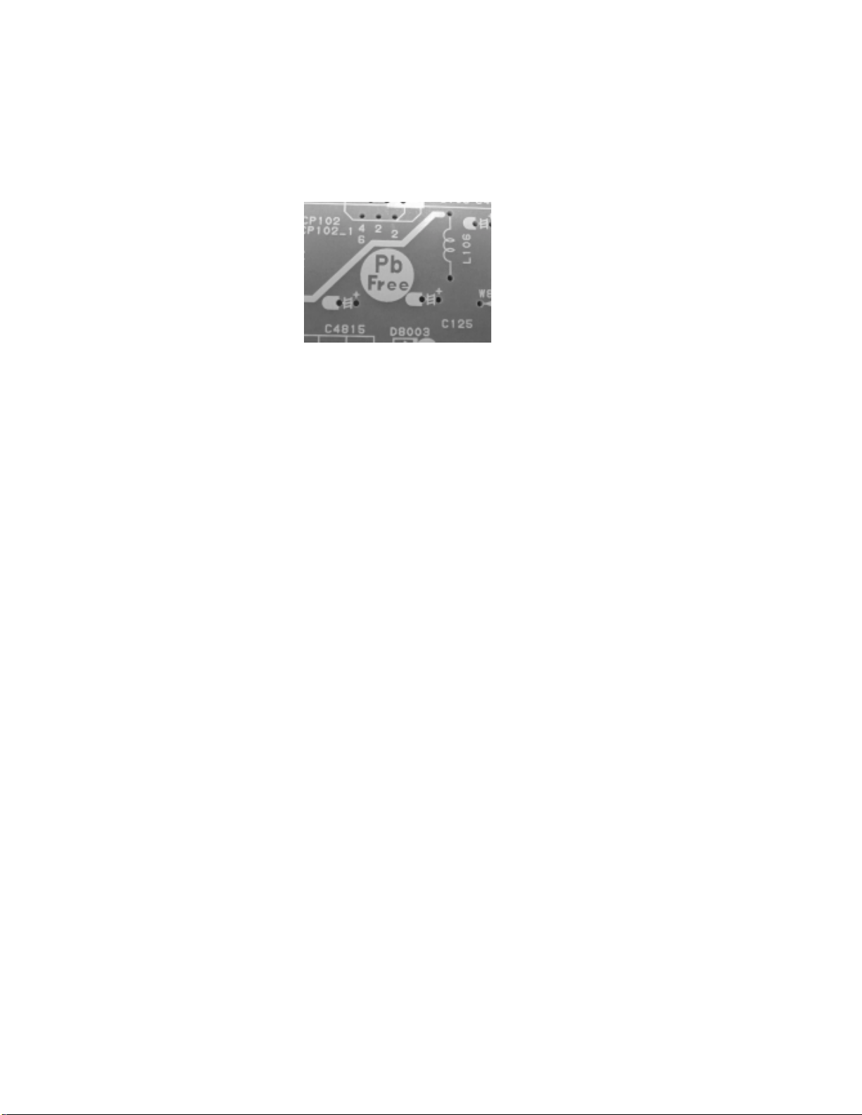
ABOUT LEAD FREE SOLDER (PbF)
Distinction of PbF PCB:
PCBs (manufactured) using lead free solder will have a PbF printing on the PCB.
(Please refer to figures.)
Caution:
Pb free solder has a higher melting point than standard solder;
•
Typically the melting point is 50°F~70°F(30°C~40°C) higher.
Please use a soldering iron with temperature control and adjust it to 650°F ± 20°F (350°C ± 10°C).
In case of using high temperature soldering iron, please be carefull not to heat too long.
Pb free solder will tend to splash when heated too high (about 1100°F/ 600°C).
•
All products with the printed circuit board with PbF printing must be serviced with lead free solder.
•
When soldering or unsoldering, completely remove all of the solder from the pins or solder area,
and be sure to heat the soldering points with the lead free solder until it melts sufficiently.
Recommendations
Recommended lead free solder composition is Sn-3.0Ag-0.5Cu.
A1-2
20AF45/20AF45C

TABLE OF CONTENTS
SERVICING NOTICES ON CHECKING.....................................................................................
HOW TO ORDER PARTS ..........................................................................................................
IMPORTANT ...............................................................................................................................
ABOUT LEAD FREE SOLDER (PbF)........................................................................................
TABLE OF CONTENTS..............................................................................................................
GENERAL SPECIFICATIONS ...................................................................................................
DISASSEMBLY INSTRUCTIONS
1. REMOVAL OF ANODE CAP ...............................................................................................
2. REMOVAL AND INSTALLATION OF FLAT PACKAGE IC ................................................
SERVICE MODE LIST ................................................................................................................
CONFIRMATION OF HOURS USED .........................................................................................
WHEN REPLACING EEPROM (MEMORY) IC ..........................................................................
ELECTRICAL ADJUSTMENTS..................................................................................................
BLOCK DIAGRAMS ...................................................................................................................
PRINTED CIRCUIT BOARDS
MAIN/CRT................................................................................................................................
SCHEMATIC DIAGRAMS
MICON .....................................................................................................................................
CHROMA .................................................................................................................................
DEFLECTION ..........................................................................................................................
POWER ...................................................................................................................................
SOUND ....................................................................................................................................
TUNER/STEREO.....................................................................................................................
COMB/FILTER/AV...................................................................................................................
CRT..........................................................................................................................................
WAVEFORMS .............................................................................................................................
MECHANICAL EXPLODED VIEWS...........................................................................................
MECHANICAL REPLACEMENT PARTS LIST .........................................................................
ELECTRICAL REPLACEMENT PARTS LIST...........................................................................
A1-1
A1-1
A1-1
A1-2
A2-1
A3-1~A3-10
B1-1
B2-1, B2-2
C-1
C-1
C-1
D-1~D-6
E-1, E-2
F-1~F-4
G-1, G-2
G-3, G-4
G-5, G-6
G-7, G-8
G-9, G-10
G-11, G-12
G-13, G-14
G-15, G-16
H-1, H-2
I-1, I-2
J1-1, J1-2
J2-1~J2-8
A2-1
20AF45/20AF45C
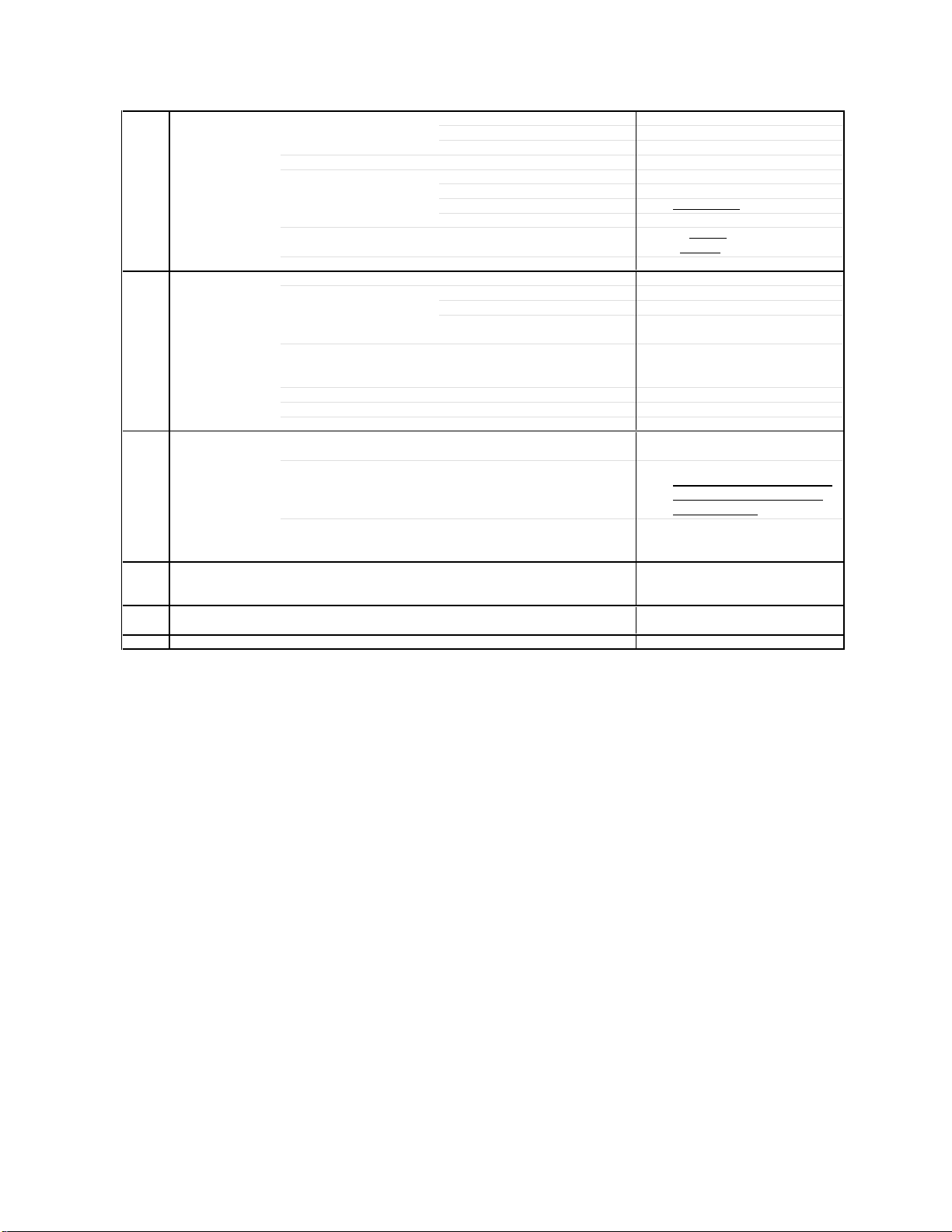
GENERAL SPECIFICATIONS
G-1 TV CRT CRT Size / Visual Size 20 inch / 508mmV
G-2 Tuning Broadcasting System US System M
G-3 Power Power Source AC 120V AC 60Hz
G-4 Regulation Safety UL
G-5 Temperature Operation +5oC ~ +40oC
G-6 Operating Humidity Less than 80% RH
System CRT Type Flat
Color System NTSC
Speaker 2 Speaker
Sound Output MAX
NTSC3.58+4.43 /PAL60Hz No
System Tuner and System 1Tuner
Receive CH Destination USA(W/ CATV)
Intermediate Picture(FP) 45.75MHz
Frequency Sound(FS) 41.25MHz
Preset CH
Stereo/Dual TV Sound Yes
Tuner Sound Muting Yes
Power Consumption at AC
Protector Power Fuse Yes
Magnetic Field BV/BH +0.45G/0.18G
Position Front Side
Size 2 x 4.7 Inch
Impedance 8 ohm
2.5+2.5 W
10%(Typical) - W
CH Coverage A - I, J - W, W+1 - W+84
FP-FS 4.50MHz
DC
105 W at AC 120 V 60 Hz
Stand by (at AC) 3 W at AC 120 V 60 Hz
Per Year -- kWh/Year
Safety Circuit Yes
IC Protector(Micro Fuse) No
Radiation FCC
X-Radiation DHHS
Storage -20oC ~ +60oC
2 - 69, 4A, A-5 - A-1,
No
A3-1 20AF45
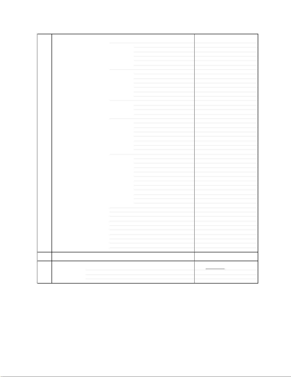
GENERAL SPECIFICATIONS
G-7 On Screen Menu Yes
G-8 OSD Language English French Spanish
Display Menu Type Icon
Picture Yes
Sound Yes
Set Up Yes
Option
Control Level Yes
Stereo,Audio Output,SAP Yes
Video Yes
Color Stream Yes
Channel(TV/Cable) Yes
CH Label Yes
Game Timer Yes
Sleep Timer Yes
Sound Mute Yes
V-chip Rating Yes
16: 9 Yes
Contrast Yes
Brightness Yes
Color Yes
Tint Yes
Sharpness Yes
Bass Yes
Treble Yes
Balance Yes
BBE On/Off No
Stable Sound On/Off Yes
Surround On/Off Yes
TV/CATV Yes
Auto CH Memory Yes
Add/ Delete Yes
Yes
Language Yes
CH Label Yes
Favorite CH Yes
V-Chip Yes
Lock Yes
On/Off Timer Yes
Color Stream DVD/DTV Yes
Volume Yes
Brightness Yes
Contrast Yes
Color Yes
Tint Yes
Sharpness Yes
Tuning No
Bass Yes
Treble Yes
Balance Yes
Back Light No
G-9 Clock and Sleep Timer Max Time 120 Min
Timer Step
On/Off Timer Program(On Timer / Off Timer / Clock) Yes
Wake Up Timer No
Timer Back-up (at Power Off Mode) more than -- Min Sec
10 Min
A3-2 20AF45
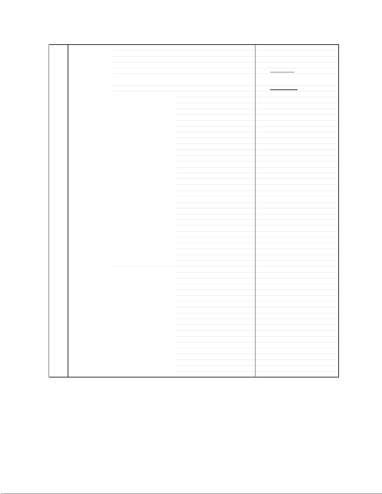
GENERAL SPECIFICATIONS
G-10 Remote Unit RC-GQ
Control Glow in Dark Remocon Yes
Format Toshiba
Remocon Format Toshiba
Custom Code
Power Source Voltage(D.C) 3V
UM size x pcs UM-4 x 2 pcs
Total Keys
Keys Power Yes
1 Yes
2 Yes
3 Yes
4 Yes
5 Yes
6 Yes
7 Yes
8 Yes
9 Yes
0 Yes
100 Yes
CH Up Yes
CH Down Yes
Volume Up Yes
Volume Down Yes
Cap/Text(TV/Caption/Text) Yes
1/2(CH1/CH2) Yes
TV/Video(TV/AV) Yes
CH RTN(Quick View) Yes
Sleep Yes
RECall(Call) Yes
Reset Yes
Menu/Enter Yes
Mute Yes
Exit Yes
MTS(Audio Select) Yes
Fav.Up Yes
Fav.Down Yes
16: 9 Yes
Multi Brand Keys CH Up(VCR) No
CH Down(VCR) No
Pause/Still No
TV/VCR(VCR) No
FF No
Rew No
Rec No
Play No
Stop No
TV No
VCR No
Cable No
DVD No
CODE No
DVD MENU < No
DVD MENU > No
DVD CLEAR No
TOP MENU No
DVD MENU No
TV:40-BF h
30 Keys
A3-3 20AF45
GENERAL SPECIFICATIONS
G-11 Features Auto Degauss Yes
G-12 Accessories Owner's Manual Language English/Spanish
Auto Shut Off Yes
Canal+ No
CATV Yes
Anti-theft No
Rental No
Memory(Last CH) Yes
Memory(Last Volume) Yes
V-Chip Yes
Type
BBE No
Auto Search No
CH Allocation No
SAP Yes
Just Clock Function No
CH Label Yes
VM Circuit No
Full OSD No
Premiere No
Comb Filter Yes
Auto CH Memory Yes
Hotel Lock No
Closed Caption Yes
Stable Sound Yes
FBT Leak Test Protect Yes
CH Lock Yes
Video Lock Yes
Game Timer (Max Time:120 Min) Yes
Energy Star No
Favorite CH Yes
Surround Yes
16:9 Mode Yes
W/ Warranty Yes
Remote Control Unit Yes
Rod Antenna
Poles
Terminal
Loop Antenna
Terminal -
U/V Mixer
DC Car Cord (Center+)
Guarantee Card
Warning Sheet
Circuit Diagram
Antenna Change Plug
Service Station List
Important Safety Instruction
Dew/AHC Caution Sheet
AC Plug Adapter
Quick Set-up Sheet
Battery Yes
UM size x pcs UM-4 x 2
OEM Brand
AC Cord
AV Cord (2Pin-1Pin)
Registration Card (NDL Card) Yes
PTB Sheet
ESP Card
300 ohm to 75 ohm Antenna Adapter
USA,Toshiba Type
2 Lines
No
No
No
No
No
No
No
No
No
No
No
No
No
No
No
No
No
No
No
A3-4 20AF45
GENERAL SPECIFICATIONS
G-13 Interface Switch Front Power Yes
Rear AC/DC No
Indicator Power Yes(RED)
Terminals Front Video Input = VIDEO2
Rear Video Input(Rear1) = VIDEO1
G-14 Set Size Approx. W x D x H (mm)
G-15 Weight Net (Approx.) 23 kg
G-16 Carton Master Carton
Gift Box Material Double/Brown
Drop Test
Container Stuffing
G-17 Cabinet Material Cabinet Cabinet Front PS 94V0 DECABROM
PCB Non-Halogen Demand
G-18 Environment Pb-free Soldering Yes
Parts Specification(Phase3 : based on RoHS) Yes
System Select No
Main Power SW No
Sub Power No
Channel Up Yes
Channel Down Yes
Volume Up Yes
Volume Down Yes
TV/CATV Selector No
Degauss No
Main Power SW No
Stand-by No
On Timer No
Audio Input = VIDEO2
Other Terminal
Video Input(Rear2) = VIDEO2 No
Audio Input(Rear1) = VIDEO1
Audio Input(Rear2) = VIDEO2 No
Video Output No
Audio Output No
Euro Scart No
Color Stream
S Input Yes
Diversity No
Ext Speaker No
DC Jack 12V(Center +) No
VHF/UHF Antenna Input
AC Outlet No
Gross (Approx.) 26.5 kg
Content ---Material --
Dimensions W x D x H(mm) -- x -- x --
Description of Origin
Dimensions W x D x H(mm) 695 x 575 x 549
Description of Origin Yes
Height (cm) 60 (ORION SPEC:46)
Cabinet Rear PS 94V0 DECABROM
Eyelet Demand Yes
RCA
RCA x 2
Head Phone
RCA
RCA x 2
RCA x 3
F Type
590 x 484 x 446.5
( 50.6 lbs)
( 58.3 lbs)
No
Sets
/--
No
Natural Dropping At 1 Corner / 3
Edges / 6 Surfaces
272
Sets/40' container
No
A3-5 20AF45
GENERAL SPECIFICATIONS
G-1 TV CRT CRT Size / Visual Size 20 inch / 508mmV
G-2 Tuning Broadcasting System US System M
G-3 Power Power Source AC 120V AC 60Hz
G-4 Regulation Safety CSA
G-5 Temperature Operation +5oC ~ +40oC
G-6 Operating Humidity Less than 80% RH
System CRT Type Flat
Color System NTSC
Speaker 2 Speaker
Sound Output MAX
NTSC3.58+4.43 /PAL60Hz No
System Tuner and System 1Tuner
Receive CH Destination USA(W/ CATV)
Intermediate Picture(FP) 45.75MHz
Frequency Sound(FS) 41.25MHz
Preset CH
Stereo/Dual TV Sound Yes
Tuner Sound Muting Yes
Power Consumption at AC
Protector Power Fuse Yes
Magnetic Field BV/BH +0.45G/0.18G
Position Front Side
Size 2 x 4.7 Inch
Impedance 8 ohm
2.5+2.5 W
10%(Typical) - W
CH Coverage A - I, J - W, W+1 - W+84
FP-FS 4.50MHz
DC
105 W at AC 120 V 60 Hz
Stand by (at AC) 3 W at AC 120 V 60 Hz
Per Year -- kWh/Year
Safety Circuit Yes
IC Protector(Micro Fuse) No
Radiation IC
X-Radiation HWC
Storage -20oC ~ +60oC
2 - 69, 4A, A-5 - A-1,
No
A3-6 20AF45C
 Loading...