

Page 1

TOSHIBA
SERVICE MANUAL
FILE NO.050-200102
COLOR TELEVISION
20AF41C
DOCUMENT CREATED IN JAPAN, DEC., 2001
Page 2
SERVICING NOTICES ON CHECKING
As for the places which need special attentions,
they are indicated with the labels or seals on the
cabinet, chassis and parts. Make sure to keep the
indications and notices in the operation manual.
2. AVOID AN ELECTRIC SHOCK
There is a high voltage part inside. Avoid an
electric shock while the electric current is
flowing.
3. USE THE DESIGNATED PARTS
The parts in this equipment have the specific
characters of incombustibility and withstand
voltage for safety. Therefore, the part which is
replaced should be used the part which has
the same character.
Especially as to the important parts for safety
which is indicated in the circuit diagram or the
table of parts as a mark, the designated
parts must be used.
4. PUT PARTS AND WIRES IN THE
ORIGINAL POSITION AFTER
ASSEMBLING OR WIRING
There are parts which use the insulation
material such as a tube or tape for safety, or
which are assembled in the condition that
these do not contact with the printed board.
The inside wiring is designed not to get closer
to the pyrogenic parts and high voltage parts.
Therefore, put these parts in the original
positions.
5. TAKE CARE TO DEAL WITH THE
CATHODE-RAY TUBE
In the condition that an explosion-proof cathoderay tube is set in this equipment, safety is
secured against implosion. However, when
removing it or serving from backward, it is
dangerous to give a shock. Take enough care to
deal with it.
6. AVOID AN X-RAY1. KEEP THE NOTICES
Safety is secured against an X-ray by considering about the cathode-ray tube and the high
voltage peripheral circuit, etc.
Therefore, when repairing the high voltage peripheral circuit, use the designated parts and
make sure not modify the circuit.
Repairing except indicates causes rising of high
voltage, and it emits an X-ray from the cathoderay tube.
PERFORM A SAFETY CHECK AFTER
7.
SERVICING
Confirm that the screws, parts and wiring which
were removed in order to service are put in the
original positions, or whether there are the
portions which are deteriorated around the
serviced places serviced or not. Check the
insulation between the antenna terminal or
external metal and the AC cord plug blades.
And be sure the safety of that.
(INSULATION CHECK PROCEDURE)
1.
Unplug the plug from the AC outlet.
2.
Remove the antenna terminal on TV and turn
on the TV.
3.
Insulation resistance between the cord plug
terminals and the eternal exposure metal
[Note 2] should be more than 1M ohm by
using the 500V insulation resistance meter
[Note 1] .
4.
If the insulation resistance is less than 1M
ohm, the inspection repair should be
required.
[Note 1]
If you have not the 500V insulation
resistance meter, use a Tester.
[Note 2]
External exposure metal: Antenna terminal
Earphone jack
HOW TO ORDER PARTS
Please include the following informations when you order parts. (Particularly the VERSION LETTER.)
1. MODEL NUMBER and VERSION LETTER
The MODEL NUMBER can be found on the back of each product and the VERSION LETTER can be
found at the end of the SERIAL NUMBER.
2. PART NO. and DESCRIPTION
You can find it in your SERVICE MANUAL.
IMPORTANT
Inferior silicon grease can damage IC's and transistors.
When replacing an IC's or transistors, use only specified silicon grease (YG6260M).
Remove all old silicon before applying new silicon.
Licensed by BBE Sound, Inc. under USP4638258 and 4482866.
BBE and BBE symbol are registered trademarks of BBE
Sound, Inc.
Page 3
GENERAL SPECIFICATIONS
G-1.Ou tline of t he Product
20 inch( 508.0
Color CRT 90 degree deflection
G-2.Broadcasting System
US System M
G-3.Color System NTSC PAL SECAM or Monochrome signal
mmV):Measured diagonally
G-4.NTSC Playback(PAL 60Hz)
G-5.NTSC 3.58+4.43/PAL60Hz
G-6.An tenna Input Impedance
VHF/UHF 75 ohm unbalanced
G-7.Tuner and Receiving Contactless Electric tuner
channel Tuner
channel coverage
(USA) 2~69 , 4A ,
Tuning System
Frequency syn. Voltage syn. Others
G-8.Preset Channel
-- channels
G-9.Intermediate Frequency
Picture(fP) 45.75 MHz
Sound (fS) 41.25 MHz MHz MHz
fP-fS 4.50 MHz MHz MHz
G-10.Stereo/Dual TV Sound
Yes( NICAM GERMAN USA JAPAN) No
G-11.Tune r S ound Muting
Oscar(W/O HYPER) Oscar(W/ HYPER)
France CATV) Others
A-5~A-1, A~I , J~W, W+1~W+84
Yes No
Yes No
Yes No
1Tuner System
2Tuner System
MHz MHz
G-12.Power Source 120 V
G-13.Power Consumption: 105 W at AC 120 V 60 Hz
- W at DC V
Stand by: 4 W at AC 120 V 60 Hz
Per Year: kWh / Year
G-14.Dimensions(Approx.)
590 mm(W) 487.5
G-15.Weight(Approx.) Net : 23 kg ( 50.6 lbs)
Gross: 26.5 kg ( 58.3 lbs)
G-16.Cabinet Material
Cabinet Front:
Back Pane l:
G-17.Protector:
Power Fuse
mm(D) 444 mm(H)
PS 94HB DECABROM
ABS 94V2 NON-DECA
PS 94HB DECABROM
ABS 94V2 NON-DECA
AC 50Hz AC 60Hz
94V0
94V0
Page 4
GENERAL SPECIFICATIONS
G-18.Regulation
Safety
UL CSA SAA SI CE SEV
BS NF NEMKO FEMKO DEMKO IEC65
SEMKO NZ HOMOLO SABS CNS SISIR
NOM AS3159 DENTORI UNE GOST NONE
Radiation
FCC DOC FTZ PTT CE SEV
SABA SI NF NZ HOMOLO UNE
CNS CISPR13 DENTORI AS/NZS NONE
X-Radiation
PTB DHHS HWC DENTORI NONE
G-19.Temperature
Operation 5 ºC~ 40
Storage -20 ºC~ 60 ºC
G-20.Operating Humidity Less than 80 %RH
G-21.Clock and Timer
Sleep Timer
On/Off Timer Yes Programs No
Wake Up Timer Yes Programs No
G-22.Timer back up Ti me
More than -- Minutes (at Power Off Mode)
G-23.Terminals
VHF/UHF Antenna Din Type F-Type France Type
Video Input(Front) (RCA ø8.3x 1)
Video Input(Rea r 1) (RCA ø8.3x1)
Video Input(Rea r 2) (RCA ø8.3x1)
Video Output(Rear) (RCA ø8.3x1)
Audio In put(Front) (RCA ø8.3x2)
Audio In put(Rear1) (R CA ø8.3x2)
Audio In put(Rear2) (R CA ø8.3x2)
Audio Output(Rear) (RCA ø8.3x2)
21 Pin (x ) DC Jack(Center +) Ear Phone Jack(ø3. 5)
Head Phone Jack(ø3.5) AC Outlet Ext Speaker
Diversity S Input(Front) S Input(Rear)
Color Streem (RCA ø8.3x3 )
G-24.Indicator
Power Stand By On Timer NONE
( RED ) (
G-25.Display
On Screen Display
Menu (Windows Type/Picture Menu)
Picture
SOUND
SETUP
OPTION
Contro l Level Sound Brightness Contrast
Stereo,Audio Output,SAP Video ColorStream
Channel CH Label Sleep Timer Sound Mute
V-Chip Rating
) ( )
Contrast Brightness Color Tint Sharpness
Bass Treble Balance
BBE ON/OFF Stable Sound ON /OFF
TV/CATV CH Prpgram Add/Erase
Language CH Label Favorit e CH
V-CHIP Color Streem DVD/DTV
Color Tint(NTSC Only) Sharpness
Tuning Bass Treble
Balance Back Light
ºC
Yes Max 120 Min.( 10 Min. Step) No
Page 5
GENERAL SPECIFICATIONS
G-26.O S D Language
Eng Ger Fre Spa Ita Por Jpn
OSD Language Se tting
Eng Ger Fre Spa Ita Por Jpn
Not Appl icable
G-27.Speaker
Pos ition
Size 2x4.7 inches
Imp 8 ohm x 2 pcs
Power Max 2.5 + 2.5 W
G-28.EX T Speaker
Yes - W Imp - ohm NO
G-29.Carton
Master Carton:
Content: ---- Set
Material: ---- / ---- Corrugated Carton
Dimensions: ---- mm(W) ---- mm(D) ---- mm(H)
Description of Origin Yes No
Gift Box
Material
Dimensions: 658 mm(W) 575
Design: As Per BUYER 's
Description of Origin: Yes No
Drop Test Natural Dropping At 1 Corner / 3 Edges / 6 Surfaces
Container Stuffing: 288 Sets / 40' container
Need No Need
Double/Brown Corrugated Carton ( with Ph oto Label)
Double/White Corrugated Carton ( with Photo Label)
Double Full Color Carton W/Photo
Height
Front Side Bottom
10% 2.0 + 2.0 W (Typical)
mm(D) 529 mm(H)
25cm 31cm 46cm 62cm 80cm
G-30.Accessories
Owner's Manual ( W/Wa rranty) [English/French]
Channel Film
AC Plug Adapter Remote Control Unit
Battery (UM- 4 x 2 )
Safety Tip Toll Free Insert Sheet
Guarantee Ca rd Audio-Video Cord (RCA)
Registration/Warranty Card Warning Sheet
Quick Se t-Up Sheet Schematic Diagram
Information Sheet U/V Mixer
75 ohm Coaxial Cable ( Single Shield Double Shield)
300 ohm to 75 ohm Antenna Plug
21pin Cable Car Cord
Rod Ant enn a
One Pole Two Pole ( F-Type Din Type France Type)
Loop Antenna ( F-Type Din Type France Type)
Importan t Safety Instructi ons Service St a ti on List
Envelope
Page 6
G-31.Other Features
Auto Degauss Auto Search Full OSD
Auto Shut Off CH Allocation Premiere
Canal+ SAP Comb Filter(3 LIN E)
CATV Channel Lock Auto CH Memory
Anti-Theft Just Clock Function Hotel Lock
Rental Game Position Closed Caption
Memory ( Last CH Last Vol.) Stable Sound
V-Chip(Toshiba Type) CH LAVEL Favorit e CH
BBE VM Circuit
G-32.Switch
Front
Power(Tact) Channel Up Volume Up
System Select Channel Down Volume Down
Main Power SW Sub Power
Rear
AC/DC TV/CATV Selector
Degauss Main Power SW
G-33.Magnetic Fiel d
BV : +0.45G BV : +0.35G BV : +0.25G
BH : 0.18G BH : 0.30G BH : 0.30G
BV : -0.15G BV : -0.25G BV : -0.50G
BH : 0.15G BH : 0.15G BH : 0.30G
GENERAL SPECIFICATIONS
G-34.Remote Control Unit: RC-DU
Glow in Dark Remocon Yes No
Power Source: D.C 3 V Battery UM - 4 x 2
Total 42 Key
Power
0 Muting TV/Video(TV/AV)
1 TV/Caption/Text Volume Up
2 CH1/CH2 Volume Down
3 Sleep MT S( A ud io S elect)
4 RE Call(Ca ll) CH Down
5 Reset CH Up
6 Menu/Enter FAV. UP
7 EXIT FAV. DOWN
8 CH RTN/CH ENT(Quick View)
9
100
Multi Brand Key
CH Up(VCR) FF TV
CH Down(VCR) Rec VCR
Pause/Still Stop Cable
TV/VCR(VCR) Rew Play
CODE
Page 7
DISASSEMBLY INSTRUCTIONS
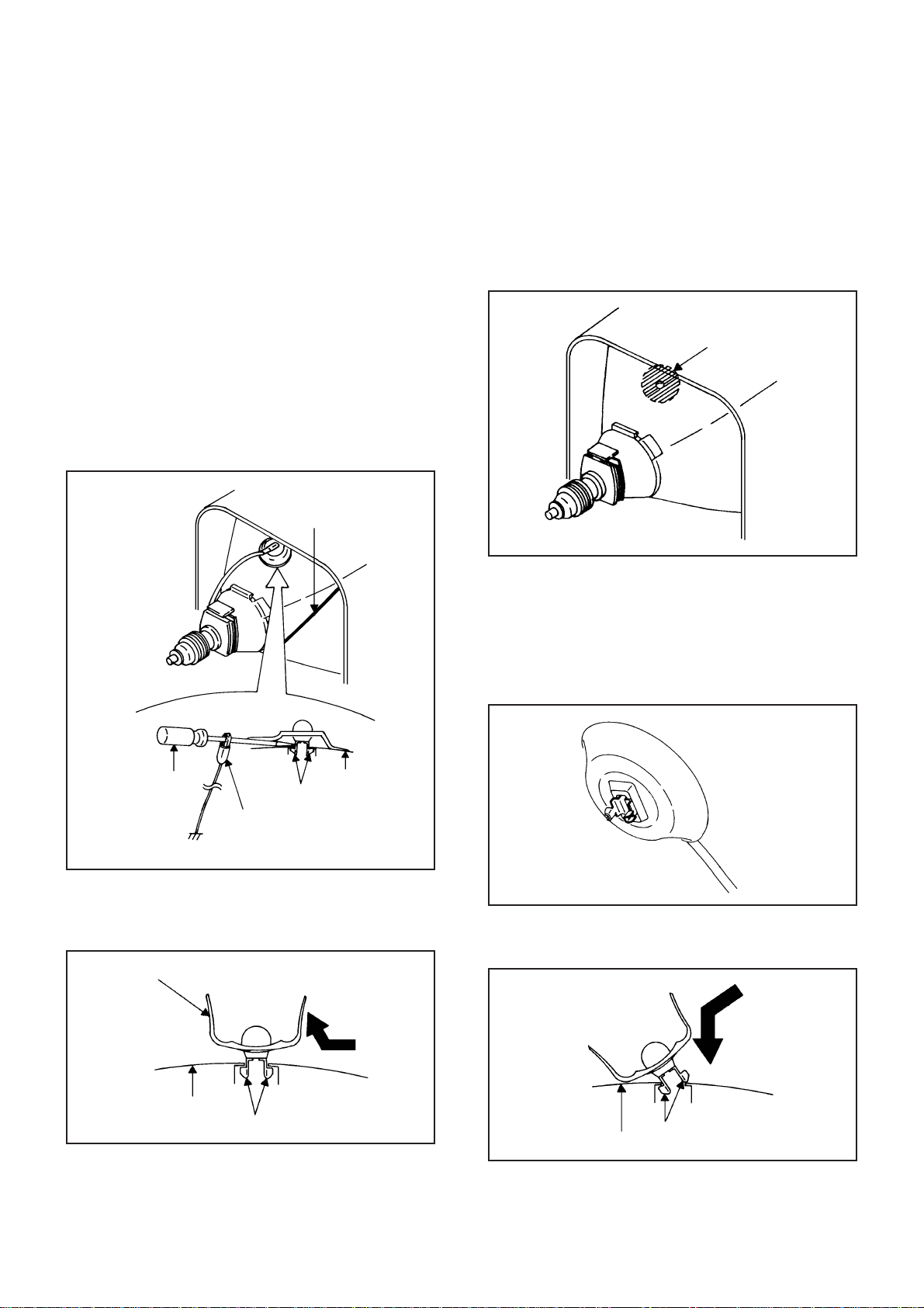
1. REMOVAL OF ANODE CAP
Read the following NOTED items before starting work.
*
After turning the power off there might still be a potential
voltage that is very dangerous. When removing the
Anode Cap, make sure to discharge the Anode Cap's
potential voltage.
*
Do not use pliers to loosen or tighten the Anode Cap
terminal, this may cause the spring to be damaged.
REMOVAL
1. Follow the steps as follows to discharge the Anode Cap.
(Refer to Fig. 1-1.)
Connect one end of an Alligator Clip to the metal part of a
flat-blade screwdriver and the other end to ground.
While holding the plastic part of the insulated Screwdriver,
touch the support of the Anode with the tip of the
Screwdriver.
A cracking noise will be heard as the voltage is discharged.
GND on the CRT
3. After one side is removed, pull in the opposite direction to
remove the other.
NOTE
Take care not to damage the Rubber Cap.
INSTALLATION
1. Clean the spot where the cap was located with a small
amount of alcohol. (Refer to Fig. 1-3.)
Location of Anode Cap
Fig. 1-3
NOTE
Confirm that there is no dirt, dust, etc. at the spot where
the cap was located.
2.3.Arrange the wire of the Anode Cap and make sure the
wire is not twisted.
Turn over the Rubber Cap. (Refer to Fig. 1-4.)
Screwdriver
Alligator Clip
GND on the CRT
Flip up the sides of the Rubber Cap in the direction of the
2.
arrow and remove one side of the support.
(Refer to Fig. 1-2.)
Rubber Cap
CRT
Support
Support
CRT
Fig. 1-1
Fig. 1-2
Fig. 1-4
4. Insert one end of the Anode Support into the anode button,
then the other as shown in Fig. 1-5.
Support
CRT
5.6.Confirm that the Support is securely connected.
Put on the Rubber Cap without moving any parts.
Fig. 1-5
Page 8
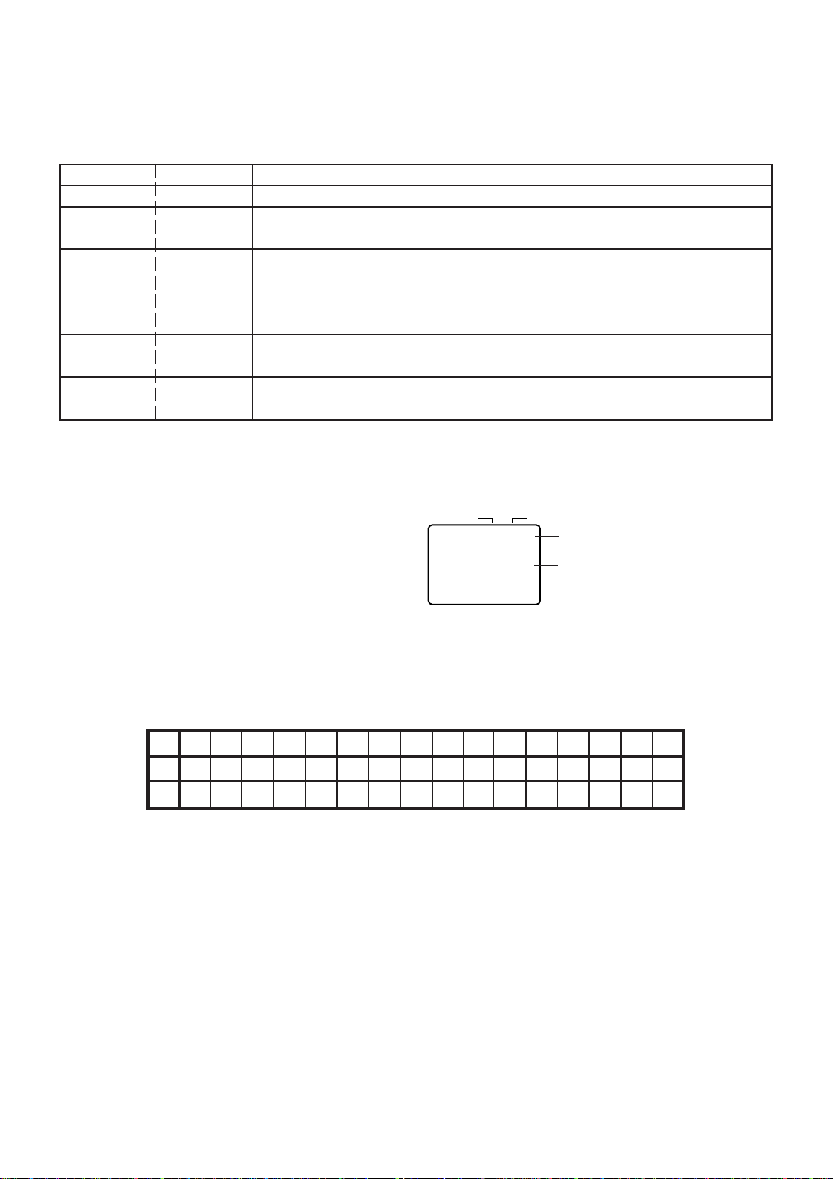
SERVICE MODE LIST
This unit provided with the following SERVICE MODES so you can repair, examine and adjust easily.
To enter the Service Mode, press both set key and remote control key for more than 1 second.
Set Key Remocon Key Operations
VOL. (-) MIN
0
Releasing of V-CHIP PASSWORD.
VOL. (-) MIN 1
VOL. (-) MIN 6
VOL. (-) MIN 8
VOL. (-) MIN
9
Initialization of the factory.
NOTE: Do not use this for the normal servicing.
POWER ON total hours is displayed on the screen.
Refer to the "CONFIRMATION OF USING HOURS".
Can be checked of the INITIAL DATA of MEMORY IC.
Refer to the "NOTE FOR THE REPLACING OF MEMORY IC".
Writing of EEPROM initial data.
NOTE: Do not use this for the normal servicing.
Display of the Adjustment MENU on the screen.
Refer to the "ELECTRICAL ADJUSTMENT" (On-Screen Display Adjustment).
CONFIRMATION OF USING HOURS
POWER ON total hours can be checked on the screen. Total hours are displayed in 16 system of notation.
1.
Set the VOLUME to minimum.
2.
Press both VOL. DOWN button on the set and Channel
button (6) on the remote control for more than 1 second.
3.
After the confirmation of using hours, turn off the power.
ADDRESS DATA
INIT 00 83
CRT ON
0010
FIG. 1
Initial setting content of MEMORY IC.
POWER ON total hours.
= (16 x 16 x 16 x thousands digit value)
+ (16 x 16 x hundreds digit value)
+ (16 x tens digit value)
+ (ones digit value)
NOTE FOR THE REPLACING OF MEMORY IC
If a service repair is undertaken where it has been required to change the MEMORY IC, the following steps should be taken to
ensure correct data settings while making reference to TABLE 1.
+0 +1 +2 +3 +4 +5 +6 +7 +8 +9
A1 C3 CF 00 31 B3 27 37 BE E8
00 F4 84 00 00 00 46
40 --- --- --- --- --- --- --- ---
10
Enter DATA SET mode by setting VOLUME to minimum.
1.
Press both VOL. DOWN button on the set and Channel button (6) on the remote control for more than 1 second.
2.
ADDRESS and DATA should appear as FIG 1.
ADDRESS is now selected and should "blink". Using the VOL. UP/DOWN button on the remote, step through the
3.
ADDRESS until required ADDRESS to be changed is reached.
Press ENTER to select DATA. When DATA is selected, it will "blink".
4.
Again, step through the DATA using VOL. UP/DOWN button until required DATA value has been selected.
5.
Pressing ENTER will take you back to ADDRESS for further selection if necessary.
6.
Repeat steps 3 to 6 until all data has been checked.
7.
When satisfied correct DATA has been entered, turn POWER off (return to STANDBY MODE) to finish DATA input.
8.
The unit will now have the correct DATA for the new MEMORY IC.
---
Table 1
+A
+B +C +D +E +FINI
--- --- --- --- --- ---
Page 9
ELECTRICAL ADJUSTMENTS
1.
BEFORE MAKING ELECTRICAL
ADJUSTMENTS
Read and perform these adjustments when repairing the
circuits or replacing electrical parts or PCB assemblies.
CAUTION
•
Use an isolation transformer when performing any
service on this chassis.
•
Before removing the anode cap, discharge electricity
because it contains high voltage.
•
When removing a PCB or related component, after
unfastening or changing a wire, be sure to put the wire
back in its original position.
Inferior silicon grease can damage IC's and transistors.
•
When replacing IC's and transistors, use only specified
silicon grease.
Remove all old silicon before applying new silicon.
Prepare the following measurement tools for electrical
adjustments.
1. Synchro Scope
2. Digital Voltmeter
On-Screen Display Adjustment
In the condition of NO indication on the screen.
1.
Press the VOL. DOWN button on the set and the
Channel button (9) on the remote control for more than
1 second to appear the adjustment mode on the screen
as shown in Fig. 1-1.
TV
00 OSD 15
Fig. 1-1
Use the Channel UP/DOWN button or Channel button
2.
(0-9) on the remote control to select the options shown
in Fig. 1-2.
Press the MENU button on the remote control to end
3.
the adjustments.
2. BASIC ADJUSTMENTS
2-1: CONSTANT VOLTAGE
1.
Set condition is AV MODE without signal.
2.
Connect the digital voltmeter to TP002.
3.
Adjust the VR502 until the digital voltmeter is 111 ± 1V.
2-2: RF AGC
1.
Receive a 70dB monoscope pattern.
2.
Connect the digital voltmeter between the TP001 and
the GND.
3.
Activate the adjustment mode display of Fig. 1-1 and
press the channel button (02) on the remote control to
select "RF. AGC".
4.
Press the VOL. UP/DOWN button on the remote
control until the digital voltmeter is 1.95 ± 0.05V.
2-3: CUT OFF
1.
Adjust the unit to the following settings.
G. DRIVE=64, B. DRIVE=64, R. BIAS=32, G. BIAS=32,
B. BIAS=32, BRIGHTNESS=70, UNI COLOR=64.
2.
Place the set with Aging Test for more than 15 minutes.
3.
Activate the adjustment mode display of Fig. 1-1 and
press the channel button (01) on the remote control to
select "CUT OFF".
4.
Adjust the Screen Volume until a dim raster is obtained.
2-4: WHITE BALANCE
NOTE: Adjust after performing CUT OFF adjustment.
1.
Place the set with Aging Test for more than 10 minutes.
2.
Receive the white 100% signal from the Pattern
Generator.
3.
Using the adjustment control, set the brightness and
contrast to normal position.
4.
Activate the adjustment mode display of Fig. 1-1 and
press the channel button (13) on the remote control to
select "R. BIAS".
5.
Using the VOL. UP/DOWN button on the remote control,
adjust the R. BIAS.
6.
Press the CH. UP/DOWN button on the remote control to
select the "G. DRV", "B. DRV", "G. BIAS" or "B. BIAS".
7.
Using the VOL. UP/DOWN button on the remote control,
adjust the G. DRV, B. DRV, G. BIAS or B. BIAS.
8.
Perform the above adjustments 6 and 7 until the white
color is looked like a white.
NO.
00
01
02
03
04
05
06
07
08
09
10
11
12
13
14
15
16
FUNCTION
OSD H
CUT OFF
RF. AGC
--H. POSI
V. POSI
H. SIZE
V. SIZE
V. CENT
V. LIN
VS. CORR
G. DRV
B. DRV
R. BIAS
G. BIAS
B. BIAS
BRI
NO.
17
18
19
20
21
22
23
24
25
26
27
28
29
30
31
32
33
FUNCTION
SUBCONT
UNI COL
--TINT
SHARP
RGB CONT
PARABOLA
TRAPEZIU
COR TOP
COR BTM
V EHT
H EHT
FM. LVL
LEVEL
SEP1
SEP2
T. STE
Fig. 1-2
2-5: FOCUS
1.
Receive a 70dB monoscope pattern.
2.
Turn the Focus Volume fully counterclockwise once.
3.
Adjust the Focus Volume until picture is distinct.
2-6: HORIZONTAL POSITION
1.
Receive the center cross signal from the Pattern
Generator.
2.
Using the remote control, set the brightness and
contrast to normal position.
3.
Activate the adjustment mode display of Fig. 1-1 and
press the channel button (04) on the remote control to
select "H. POSI".
4.
Press the VOL. UP/DOWN button on the remote
control until the right and left screen size of the vertical
line becomes the same.
Page 10
ELECTRICAL ADJUSTMENTS
2-7: HORIZONTAL SIZE
NOTE: Adjust after performing adjustments in section 2-6.
1.
Receive the monoscope pattern.
2.
Using the remote control, set the brightness and
contrast to normal position.
3.
Activate the adjustment mode display of Fig. 1-1 and
press the channel button (06) on the remote control to
select "H. SIZE".
4.
Press the VOL. UP/DOWN button on the remote
control until the SHIFT quantity of the OVER SCAN on
right and left becomes 10 ± 2%.
2-8: VERTICAL POSITION
NOTE: Adjust after performing adjustments in section 2-7.
1.
Receive the center cross signal from the Pattern
Generator.
2.
Activate the adjustment mode display of Fig. 1-1 and
press the channel button (05) on the remote control to
select "V. POSI".
3.
Press the VOL. UP/DOWN button on the remote
control until the horizontal line becomes fit to the notch
of the shadow mask.
2-9: VERTICAL SIZE
NOTE: Adjust after performing adjustments in section 2-8.
1.
Receive the crosshatch signal from the Pattern
Generator.
2.
Activate the adjustment mode display of Fig. 1-1 and
press the channel button (07) on the remote control to
select "V. SIZE".
3.
Press the VOL. UP/DOWN button on the remote
control until the rectangle on the center of the screen
becomes square.
4.
Receive a broadcast and check if the picture is normal.
2-12: CORNER CORR TOP
1.
Receive the crosshatch signal from the Pattern
Generator.
2.
Using the remote control, set the brightness and
contrast to normal position.
3.
Activate the adjustment mode display of Fig. 1-1 and
press the channel button (25) on the remote control to
select "COR TOP".
4.
Press the VOL. UP/DOWN button on the remote control
until the upper section of the both ends vertical lines are
straight.
2-13: CORNER CORR BOTTOM
1.
Receive the crosshatch signal from the Pattern
Generator.
2.
Using the remote control, set the brightness and
contrast to normal position.
3.
Activate the adjustment mode display of Fig. 1-1 and
press the channel button (26) on the remote control to
select "COR BTM".
4.
Press the VOL. UP/DOWN button on the remote control
until the bottom section of the both ends vertical lines
are straight.
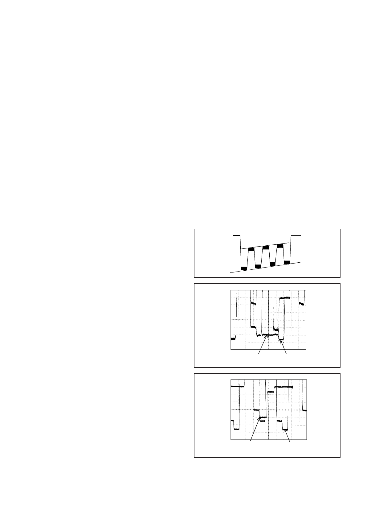
2-14: OSD HORIZONTAL
1.2.Activate the adjustment mode display of Fig. 1-1.
Press the VOL. UP/DOWN button on the remote control
until the difference of A and B becomes minimum.
(Refer to Fig. 2-1)
TV
2-10: PARABOLA
1.
Receive the crosshatch signal from the Pattern
Generator.
2.
Using the remote control, set the brightness and
contrast to normal position.
3.
Activate the adjustment mode display of Fig. 1-1 and
press the channel button (23) on the remote control to
select "PARABOLA".
4.
Press the VOL. UP/DOWN button on the remote control
until the right and left vertical lines are straight.
2-11: TRAPEZIUM
1.
Receive the crosshatch signal from the Pattern
Generator.
2.
Using the remote control, set the brightness and contrast
to normal position.
3.
Activate the adjustment mode display of Fig. 1-1 and
press the channel button (24) on the remote control to
select "TRAPEZIU".
4.
Press the VOL. UP/DOWN button on the remote control
until the both vertical lines of the screen become parallel.
00 OSD 15
A
2-15: LEVEL
1.
Receive a 70dB monoscope pattern.
2.
Connect the AC voltmeter to TP901.
3.
Activate the adjustment mode display of Fig. 1-1 and
press the channel button (30) on the remote control to
select "LEVEL".
4.
Press the VOL. UP/DOWN button on the remote
control until the AC voltmeter is 75 ± 2mV.
B
Fig. 2-1
Page 11
ELECTRICAL ADJUSTMENTS
2-16: SEPARATION 1, 2
Receive the stereo signal (L=2KHz, R=400Hz).
1.
Connect the AC voltmeter to AUDIO OUT JACK though
2.
stereo filter (L=400Hz, R=2KHz).
Activate the adjustment mode display of Fig. 1-1 and
3.
press the channel button (31) on the remote control to
select "SEP1".
Press the VOL. UP/DOWN button on the remote control
4.
until the output of L-CH and R-CH become minimum.
Press the CH UP button once the set to "SEP2" mode.
5.
Press the VOL. UP/DOWN button on the remote control
6.
until the output of L-CH and R-CH become minimum.
Press the CH DOWN button once the set to "SEP1"
7.
mode.
Repeat step 4 to step 7 several times.
8.
The output difference of the between with Filter and
without Filter should be more than 25db for both L and R.
2-17: BRIGHTNESS
1.
Activate the adjustment mode display of Fig. 1-1 and
press the channel button (16) on the remote control to
select "BRI".
2.
Press the VOL. UP/DOWN button on the remote control
until the brightness step No. becomes "68"
3.
Press the TV/VIDEO button on the remote control to set
to the AV mode. Then perform the above adjustments
1~2.
4.
Press the TV/VIDEO button on the remote control to set
to the CS mode. Then perform the above adjustments
1~2.
2-19: SUB TINT/SUB COLOR
1.
Receive the color bar pattern. (RF Input)
2.
Connect the synchro scope to TP806.
3.
Activate the adjustment mode display of Fig. 1-1 and
press the channel button (20) on the remote control to
select "TINT".
4.
Press the VOL. UP/DOWN button on the remote control
until the waveform becomes as shown in Fig. 2-2.
5.
Connect the synchro scope to TP804.
6.
Press the CH DOWN button 3 times to set to
"SUBCONT" mode.
7.
Press the VOL. UP/DOWN button on the remote control
until the red color level is adjusted to 115% of the white
level. (Refer to Fig. 2-3)
8.
Receive the color bar pattern. (Audio Video Input)
9.
Press the TV/VIDEO button on the remote control to set
to the AV mode. Then perform the above adjustments
2~7.
10.
Receive the color bar pattern. (Audio Video Input)
11.
Press the TV/VIDEO button on the remote control to set
to the CS mode. Then perform the above adjustments
2~6.
12.
Press the VOL. UP/DOWN button on the remote control
until the red color level is adjusted to 140% of the white
level. (Refer to Fig. 2-4)
2-18: UNI-COLOR
1.
Activate the adjustment mode display of Fig. 1-1 and
press the channel button (18) on the remote control to
select "UNI COL".
2.
Press the VOL. UP/DOWN button on the remote control
until the contrast step No. becomes "8"
3.
Press the TV/VIDEO button on the remote control to set
to the AV mode.
4.
Activate the adjustment mode display of Fig. 1-1 and
press the channel button (18) on the remote control to
select "UNI COL".
5.
Press the VOL. UP/DOWN button on the remote control
until the contrast step No. becomes "4"
6.
Press the TV/VIDEO button on the remote control to set
to the CS mode. Then perform the above adjustments
4~5.
White 100%
White 100%
RED Level
RED Level
Fig. 2-2
Fig. 2-3
Fig. 2-4
Page 12
ELECTRICAL ADJUSTMENTS
3.
PURITY AND CONVERGENCE
ADJUSTMENTS
NOTE
1.
Turn the unit on and let it warm up for at least 30
minutes before performing the following adjustments.
2.
Place the CRT surface facing east or west to reduce the
terrestrial magnetism.
3.
Turn ON the unit and demagnetize with a Degauss Coil.
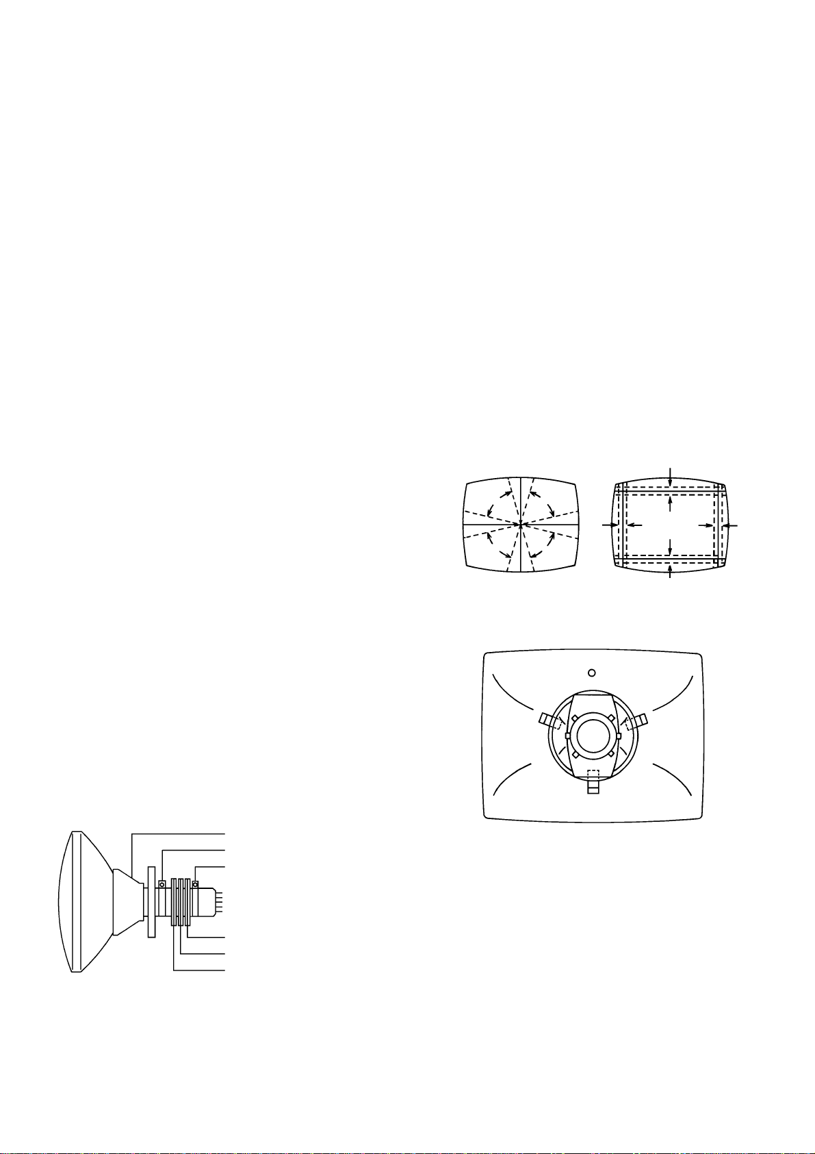
3-1: STATIC CONVERGENCE (ROUGH ADJUSTMENT)
1.
Tighten the screw for the magnet. Refer to the adjusted
CRT for the position. (Refer to Fig. 3-1)
If the deflection yoke and magnet are in one body,
untighten the screw for the body.
2.
Receive the green raster pattern from the color bar
generator.
3.
Slide the deflection yoke until it touches the funnel
side of the CRT.
4.
Adjust center of screen to green, with red and blue on the
sides, using the pair of purity magnets.
5.
Switch the color bar generator from the green raster
pattern to the crosshatch pattern.
6.
Combine red and blue of the 3 color crosshatch pattern
on the center of the screen by adjusting the pair of
4 pole magnets.
7.
Combine red/blue (magenta) and green by adjusting the
pair of 6 pole magnets.
8.
Adjust the crosshatch pattern to change to white
by repeating steps 6 and 7.
3-2: PURITY
NOTE
Adjust after performing adjustments in section 3-1.
3-3: STATIC CONVERGENCE
NOTE
Adjust after performing adjustments in section 3-2.
1.
Receive the crosshatch pattern from the color bar
generator.
2.
Combine red and blue of the 3 color crosshatch pattern
on the center of the screen by adjusting the pair of
4 pole magnets.
3.
Combine red/blue (magenta) and green by adjusting the
pair of 6 pole magnets.
3-4: DYNAMIC CONVERGENCE
NOTE
Adjust after performing adjustments in section 3-3.
1.2.Adjust the differences around the screen by moving
the deflection yoke upward/downward and right/left.
(Refer to Fig. 3-2-a)
Insert three wedges between the deflection yoke and
CRT funnel to fix the deflection yoke.
(Refer to Fig. 3-2-b)
R G B
R
G
B
UPWARD/DOWNWARD SLANT RIGHT/LEFT SLANT
R
G
B
Fig. 3-2-a
R G B
1.
Receive the green raster pattern from color bar
generator.
2.
Adjust the pair of purity magnets to center the
color on the screen.
Adjust the pair of purity magnets so the color at the
ends are equally wide.
3.
Move the deflection yoke backward (to neck side)
slowly, and stop it at the position when the whole
screen is green.
4.
Confirm red and blue colors.
5.
Adjust the slant of the deflection yoke while watching the
screen, then tighten the fixing screw.
DEFLECTION YOKE
DEFLECTION YOKE SCREW
MAGNET SCREW
PURITY MAGNETS
6 POLE MAGNETS
4 POLE MAGNETS
Fig. 3-1
WEDGE
WEDGE
WEDGE
WEDGE POSITION
Fig. 3-2-b
Page 13

TP001
TP901
MAJOR COMPONENTS LOCATION GUIDE
VR502
T501
TP002
J701
J703
J704
TU001
J702
J705
FB401
MAIN PCB
J801
CRT PCB
FOCUS VOLUME
SCREEN VOLUME
TP806
TP804
Page 14

TU001
IF
11
SDA
5
SCL
4
BLOCK DIAGRAM
MICON
IC101 OEC7054A
SCL
39
37
SDA
SPEAKER
SP351
L
12 7
SOUND AMP
IC353
AN5276
SPEAKER
SP352
R
HEAD
PHONE JACK
IF/CHROMA/AUDIO
IC201 TB1253N
38
V OUT
FBP IN
H OUT
ABCL
34
31
28
6
B OUT
16
G
B
CRT DRIVE
IF IN
G OUT
15
7
IF IN
YUV IN
24
25
SCL
SDA
R OUT
C IN
14 42 47
R
R
G
B
43 44
CVBSLNT IN
55
51
IF DET OUT
6
11
COMB FILTER
IC901
TC90A53F
8
7F10
CRT
V801
2 5
14 7
B BE
IC301
NJM2150AM
19
18
14
20 1
IC902
AN5829S
21 22
9
SDA
10 SCL
23
255
18
SCL
17
SDA
30
32
31
25
22
20
14 7
TONE CONTROL
IC303
M62420SP
19 2
24 23
AV SWITCH
IC701
MM1311AD
27 29
Y
9
C
6
Y
3
C
5
L
2
R
4
V
1
714 15 13 8 10
V
R
L
V
R
L
YUV IN
S INPUT
LINE1
1
V.OUTPUT
LA78040
5
IC401
H. OUT
Q402
Q405
DY
HV
LINE2
S
F
10
FB401
7
1
FBT
4
6
3
9
+12V
+180V
+25V
POWER SW. REG.
IC501
T501
15
13
VIDEO3
SOUND+B
+B
STR-G6624
5
4 1
3
Page 15

PRINTED CIRCUIT BOARDS
MAIN (INSERTED PARTS)
SOLDER SIDE
TP901
W111
TP001
L602
C204
L204
CF203
W810
C640
W129
C921
W138
W112
W116
W125
W124
W122
C211
W840
L901
W137
R357
R358
J351
C003
W130
C924
C929
C213
C925
W136
W119
IC353
CP902
CF201
IC201
C203
W142
W145
C918
C919
CP351
TU001
W801
D001
C004
W120
D201
C935
J712
W110
W835
C364
W844
CF202
C214
L205
CP802A
W127
R908
R705
C002
L201
L203
L202_1
C216
W133
W126
C917
R907
R707
R718
C368
W118
HS351
IC303
C304
J702
R221
C305
C604
J711
D711
C739
C740
C366
D612
W134
R330
C738
C611
CD701B
W128
C314
W123
W839
C209
X601
C310
W109
C784
C367
C630
R326
R702
C728
C744
W113
C619
C608
D614
C311
C355
L604
J701
C785
W117
W121
C615
C312
R335
C303
C328
J710
C743
L601
R708
C747
C730
W114
C612
C313
W075
C369
W115
R608
W078
C329
L302
C302
W147
L603
W132
R778
W036
C624
C616
W131
L301
W104
R743
C737
C729
L703
B501
W035
W069
C625
W061
R141
J703
C745
C733
W054
W042
W041
W040
W802
D604
W093
C351
L701
L505
W071
C610
W842
R128
R139
W144
C724
C725
IC701
W044
D603
D611
W101
W085
R131
C326
J704
CD701A
W146
C735
W051
W049
W045
W038
CP901
W070
W068
W064
D602
D613
W098
W099
W100
W094
W089
W084
W805
D107 D104
W055
W053
W039
W034
C642
R635
C711
W056
W087
W077
D102
W834
C715
W072
W066
W058
W103
R142
W047
W074
W083
IC101
R786
J705
W060
W090
W082
W048
W037
W062
W107
C783
W073
W063
W059
W102
R109
W108
W106
C705
C714
R517
W830
W095
W092
W046
W816
W820
R107
W105
D605
C741
W079
C713
C122
C111
W081
IC199
D103
W043
R430
W804
R
416_1
W811
W809
CP101
D406
W088
W080
W033
W032
W065
C436
W091
D404
C116
R421
R429
R407
W015
W013
W017
W067
Q403
X101
IC103
W026
R413
C439
CP851A
D401
R408
R404
C532
W823
L101
C407
C406
R422
R432
C427
R418
D402
HS502
IC503
R522
W018
W822
C415
R437
R410
W016
Q401
C530
W022
R414
TP002
C408
W025
C119
R440
C412
C504
C117
C428
CP401
C417
C414
Q402
IC502
W020
W829
W014
C403
W024
C529
C118
W028
W027
R423
R519
D525
C409
W012
C401
W031
W139
L401
W021
R001
D517
HS401
T401
W023
W019
R426
R521
C430
C411
IC401
C402
Q508
Q510
Q501
C422
C501_1
W813
W808
W011
R428
R529
R528
Q404
HS402
R406
W827
R520
C418
C425_1
C527
C523
D411
L402
C531
C521
R441
R436
W837
C424
Q405
C516
D505
D519
D513
SW102SW101SW104SW103
C426
W005
R
439
D408
W843
5
C
R434
_
7
1
C421
1
W010
C413
D512
D511
W008
C533
W143
D514
W825
W007
R508
CP801A
C536
B504
Q507
D510
W817
VR502
W140
C423
C416
R554
R553
D409
D528
D108
R431
C420_1
R411
R509
R137
W006
C519
D508
C419
TH501
RY501
Q504
R523
R515
Q502
D109
D407
D412
D405
D520
D507
R503
D516
CP502
C123
C506
C513
D504
OS101
IC501
T501
R502
C503
SW105
B505
CP503
FB401
W004
C502
514
C
HS501
C535_1
D515
D518
R543
B502
R542
R506
D506
D521
CP504
C510
R505
D503
D501
L501
D502
FH502 F501
- REPLACE AS MARKED.
RISK OF FIRE
W003
W002
R438
W845
TP003
TP004
W001R425
C522
C507
R501
R500
C505
CP501 FH501
Page 16

PRINTED CIRCUIT BOARDS
MAIN (CHIP MOUNTED PARTS)
SOLDER SIDE
C524
C512
C509
R533
R532
C554
R510
R511
R504
R126
Q406
R101
R511
R412
R435
Q509
C405
R525
R524
R403
R104
R405
R111
R134
R417
R415
R133
R409
R402
R419
C132
C438
Q105
R605
R442
R401
C113
R150
Q109
C114
R138
R103
C128
C124
Q103
R106
C120
R102 C121
C101
R113
R752
C109
R112
R110
R108
R751
C108
R116
C107
R725
R114
R701
R719
R124
R115
Q709
R736
R125
R119
Q101
R127
R136
C131
R724
C706
C130
C734
R755
R730
R151
R726
Q102
R130
C731
R154
R117
R118
R604
R781
R721
Q704
R322
R132
C112
R607
Q705
R737
R121
R129
C717
C722
C703
R722
R727
C135
C620
Q701
C723
R757
R738
R140
C621
R731
R123
C622
R618
R321
R314
R122
C638
R734
C325
C617
C626
R624
R362
R756
R603
R625
C748
R319
R324
R617
C708
R632
C636
C632
R740
C330
C609
C631
R616
C720
C726
C334
R320
R333
C623
R711
C333
R323
R750
R602
Q601
C793
C331
C633
R615
R622
R723
R728
C332
R623
C628
R621
R620
C727
C742
C339
R331
C607
R613R614
R619
R633
C602
Q351
C335
R327
R305
R747
C637
R355
R758
C336
R325
C606
R611
R612
C627
C353_1C352_1
R328
IC301
R609
R610
R361
R363
R716
C750
R732
C337
C338
Q604
R356
R715
C967
C966
R303
C306
R301
C308
C605
C603
C601
C618
C629
R217
C365_1
R302
C307
R636
C746
R304
C634
C222
R219
C220
R905
R904
C309
C215
R209
C208
R218
C363_1
C380C384
C212
C206
Q204
R205
C201
C218
R739
C928
C926
C959
R360
C210
C202
IC902
C965
R906
Q201
Q202
R212
R210
R202C221
R220
R211
R201
R006
C931
C922
R203
R204
C008
C001
R007 C005
R223
R214
Q203
R213
R215
R909
C932
C930
C927
C006
C007
Page 17

PRINTED CIRCUIT BOARDS
COMB FILTER (INSERTED PARTS)
SOLDER SIDE
W005
C901
CP901
L912
L911
R901
W009
L904
CP902
C908
R969
R930
L909
COMB.
L906
L903
L905
C905
W006
L902
C946
W007
C969
C947
C949
L907
W003
W002
C903
W004
L913
C909
W001
C941
L910
C953
L908
IC903
W008
C968
C962
C970
CRT/VM COIL (INSERTED PARTS)
SOLDER SIDE
R868
B853
C858
R867
R869
Q857
Q853 Q851
W815
R803
R881
C861
D852
C823
W814
C860
R875
Q855
Q854
Q852
W012
R873
R876
R871
C815
D858
R874
R870
C851
C813
D855
R816
W813
D857
D856
R857
R880
W014
R877
R872
C854
C853
R851
CP852B
Q803
TP806
L804
S851
S852
CP804
R830
Q812
CP803
Q801
C863
W011
L802
R806
R804
D803
TP804
W802
R828
C864
D801
C865
C852
C821
1
R829
TP805
L803
R802
W010
Q810
CP852_1
D854
J
80
Q802
Q811
Q856
0
8
W013
D853
C859
R866
C
8
D802
R801
Q858
W803
IC851
CP802
W801
C809
Q859
C862
CP801
C866
CP851
B851
B852
C868
R879R878
R855
C822
R808
W804
Page 18

PRINTED CIRCUIT BOARDS
COMB FILTER (CHIP MOUNTED PARTS)
SOLDER SIDE
Q912
R947
R954
Q901
R964
C958
R956
R960
Q905
R929
C948
R931
C912
R937
Q904
R903
R932
R919
R959
R938
C964
R968
R966
R957
R945
R926
Q903
R928
C907
C902
C910
C937
C954
R942
C945
R922
R917
C911
R921
R924
C938
R967
R946
C961
C951
C963
R923
C906
Q909
R943
Q911
Q907
R951
R939
R940
C942
C915
C952
C914
C916
R952
C955
R948
Q906
R936
R935
R955
R949
R944
C960
R941
C940
C943
C904
R965
R958
C950
IC901
R963
C939
C944
R918
Q913
C957
Q910
R962
R953
Q908
C913
C936
CRT (CHIP MOUNTED PARTS)
SOLDER SIDE
R811
C867
R852
R859
R856
R853
C855
C856
R864
R860
R865
R861
R854
C857
R858
R821
C806
R863
R817
R862
C804
R812
R809
R815
C805
R810
R819
R813
R814
Page 19

ABC D E F GH
8
7
6
5
4
3
2
MICON / TUNER SCHEMATIC DIAGRAM
ACCESORY
BT001
R03(AB)E_20_T
TM101
BT002
R03(AB)E_20_T
FROM/TO CHROMA/IF
SYNC_OUT
AFT_OUT
FROM/TO DEFLECTION
V.OUT1 TV_MUTE
AFC SDA
X-RAY BBE_SW
FROM/TO POWER
GND_POWER P.CON+5V_W/BL
EMERGENCY2
P.CON+9V
P.FAIL DEGAUSS_H
FROM/TO AV
CV_IN
SBKMOP006A
S801X
4.8
R137
D108
W834
R152
150 1/4W
MTZJ5.6B
W804
1K
0
0
RED LED
POWER ON
SLR-342VCT32
0
5.0
D106
1SS355
SWITCH
Q107_1
DTC114TKA
D109
0
EMERGENCY
2SA1037AK
CH DOWN
Q105
S802X
PIC-23143SY2
R126
2.7K
SW102
SKHVBED010
OS101
B+
Vout
123
4.9
SW104
VOL DOWN
GND
0
5.0
1016V KA
C123
47
R111
V-BUFFER
Q101
2SC2412K
C112
R101
560
POWER
SKHVBED010
C132
R127
4.8
0
0.0022 B
820P
SW105
1K
0
C138
0.01 Y
R150
CH
4.7K
CH UP
SKHVBED010
C122
150V KA
C121
200P CH
C128
0.001 B
R129 2.2K
0
SW101
C119
0.68 TF
C118
4706.3V YK
R128
33K 1/4W
0.3
SYNC SEP.
2SC2412K
0
R104
560
VOL UP
SKHVBED010
R102
1K
R106
15K
C124
0.1 B
R131
Q109
SW103
R103
H-BUFFER
Q102
2SC2412K
C135
10K 1/4W
0.0022 B
R115
47K
R151
4.7K
R114
2.2K
R116
2.2K
SKHVBED010
1M
2
CSTS0800MG03-T2
R136
1
3
R132
X101
4.7K
W801
820
R130
4.8
0
0
15K
MICON
0
0
0
0
0
0
0
NC
0
0
110111213141516171819 220212223242526
H SYNC
V SYNC
3
NC
4
REMOCON
5
NC
6789
SYNC
KEY 1
KEY 2
X RAY
AFT
NC
NC
NC
NC
P FAIL
NC
NC
AVCC
HLF
RVCO
VHOLD
CVIN
CNVSS
X.IN
X.OUT
IC101 OEC7054A
4.8
4.8
R117
10K
4.9
R118
0
10K
0.3
5.0
5.0
C131
220P CH
C107
0.01 B
0.1
R112
0.1
10K
R113
0.1
10K
5.0
1.7
1.7
3.5
2.8
2.3
1
1.9 3.3
W823
OSD R
OSD G
OSD B
OSD BLK
X-RAY TEST
EXT MUTE
TV MUTE
BBE H
IIC OFF
POWER
H TONE OUT
SCL1
SCL2 (PIP)
SDA1
SDA2 (PIP)
SPOT KILLER
DEGAUSS H
RESET
OSC2
OSC1
50 51 52
NC
NC
40 41 42 43 44 45 46 47 48 49
AV2
AV1
31 32 33 34 35 36 37 38 39
30
VCCVSS
27 28 29
10K
R154
0
0
0
0
0
0
0
0
0
4.9
0
NC
5.0
0
5.0
0
5.0
0
4.8
NC
0
0
NC
0
NC
0
NC
5.0
3.2
5.0
2
S801Y
L101
2.7uH
D102
1SS133
2.2K 1/4W
C114
82P CH
C113
82P CH
R107
1K 1/4W
R108
2.2K
R109
R123
4.7K
R122
4.7K
R121
4.7K
W805
R125
47K
R119
47K
C130
220P CH
R124
47K
R110
10K
C108
270P CH
C109
270P CH
W822
(MAIN PCB)
TU001 NJH3022U268
IF
11
14 15
0
1.3
C008
C004
1B
C120
R139
1K 1/4W
R140
1K
R141
1K 1/4W
D107
1SS133
0
R142
47K 1/4W
R138
1K
4
5678
SDA
SCL
VSS
E2
0000
NC
10
NC
0.01 B
R001
X-RAY TEST
0
3
0
BTL
8
9
0
NC
30.0
D001
HZ30-3L
0.022 M
27K 1W
15.8
Q103
DTC114EKA
C101
0.022 B
5.05.05.0
MODE
E1
1234
C001
D104
VCC
E0
BPL
7
5.0
C002
V.S
6
NC
R006
22006.3V YK
0.01 B
1SS133
IC199
MEMORY
S-24C08ADPA-01
TEST POINT
CP101 173979-6
12345
GND
I2C SCL
R133
AGC
SDA
5
5.0
270
C005 100P CH
NC
SCL
ADRES
2
3
4
5.0
R007
C006 100P CH
1
12 13
NC
NC
4.6
6.2
1.3
270
C007
0.01 B
AGC
TP001
C003
2.250V KA
AGC
I2C OFF
I2C SDA
IC103 PST600C
VCC GND V.OUT
123
10K
C116
0.68 TF
150V KA
C111
6
R.OUT
RESET
D103
1SS133
0.68 TF
05.0 5.0
C117
R134
FROM/TO CHROMA/IF
FROM/TO DEFLECTION
FROM/TO AV
FROM/TO SOUND
FROM/TO POWER
10K
R.OUT
AGC
SCL
SDA
IF
OSD_R
OSD_G
OSD_B
OSD_BLK
X-RAY_TEST
SCL
SDA
EXT_MUTE
SCL
POWER
GND_SIGNAL
+B
AT+5V
8
7
6
5
4
3
2
1
WITH THE DIGITAL TESTER WHEN THE COLOR BROADCAST
WAS RECEIVED IN GOOD CONDITION AND PICTURE IS NORMAL.
THE DC VOLTAGE AT EACH PART WAS MEASURED
NOTE:
NOTE:THIS SCHEMATIC DIAGRAM IS THE LATEST AT THE TIME
OF PRINTING AND SUBJECT TO CHANGE WITHOUT NOTICE
CRITICAL FOR SAFETY,USE ONES
DESCRIBED IN PARTS LIST ONLY
ARESINCE THESE PARTS MARKED BYCAUTION:
DANGEREUSES AN POINT DE VUE SECURITE
N’UTILISER QUE CELLS DECRITES
DANS LA NOMENCLATURE DES PIECES
ETANTLES PIECES REPAREES PAR UNATTENTION:
PCB010
TMX481
1
ABC D E F GH
CAUTION: DIGITAL TRANSISTOR CAUTION: DIGITAL TRANSISTOR
Page 20

ABC D E F GH
C609
H OUT
470
R605
W830
0.022 B
SYNC OUT
10K
(MAIN PCB)
C638
2.2K
R632
R607
150K
X-RAY
R608
270 1/4W
30313233343536373839
DIG VDD
FBP IN/GP OUT
100P CH
C616
29
4716V KA
EW OUT
11
C617
8
FROM/TO MICON/TUNER
SYNC_OUT
SDA
SCL
0.01 B
OSD_B
OSD_G
OSD_R
OSD_BLK
R.OUT
7
6
CHROMA / IF SCHEMATIC DIAGRAM
8
7
6
FROM/TO AV
TUNER_VIDEO
FROM/TO AV
CD701B
CH244001
C.OUT
Y.OUT
S804YS804X
100016V YK
C640
0.1 B
C607
C IN
W842
W840
1016V KA
C608
0.01 B
BLACK DET FILTER
1K
R602
8
C633
0.1 B
C610
0.68 TF
09.0
40414243444546474849
V OUT
DIG GND
CVBS OUT
5
R214
270
C227
150
2.4
R223
TV BUFFER
2SA1037AK
0
Q203
3.1
R213
470P CH
L204
12uH
330
CF203
EFCT4R5MW5
S803X
TV BUFFER
Q202
2SC2412K
R210
150
1
2
3
4
9.0
3.7
AUDIO
BUFFER
3.1
Q201
2SC2412K
1.2K
R203
9.0
4.1
3.5
3.3K
R212
220
2.2K
R204
R211
C210
6
09.0
IF GND
CHROMA
IC201 TB1253N
L205
47uH
C213
470
R215
0.0022 B
C211
0.2250V KA
R205
100
4.1 2.4 2.4 3.7 2.8 3.6 2.4 2.5 1.9 2.4 2.5 2.5 2.5 2.7 1.5 6.0 4.9
IF DET OUT
LOOP FILTER
10010V
YK
C212
0.1 B
C214
IF VCC(9V)
V REF
S803Y
1016V KA
C215
DE-EMPH
D201
33P CH
MTZJ12B
1016V KA
C216
50515253545556
DC NF FILTER
C634
0.22 B
EXT AUDIO IN
C601
0.1 B
CVBS LNT IN
Y CLAMP FILTER
7
C604
APL DET FILTER
150V KA
C603
R74775R750
C605
0.1 B
U IN
CVBS EXT IN
75
C606
0.1 B
V IN
C611
C615
10010V
YK
0.47 TF
V RAMP
S802Y
L601
47uH
R604
910
R603
8.2K
2.250V KA
C612
7.1 4.0 2.1 0 6.0 3.4 2.0
H VCC(9V)
H AFC FILTER
5
FROM/TO POWER
GND_POWER
4
3
GND_SIGNAL
P.CON+9V
P.CON+5V
FROM/TO MICON/TUNER
AFT_OUT
AGC
IF
2
FROM/TO AV
FSC_OUT
TUNER_AUDIO_L
TUNER_AUDIO_R
1
THE RESISTOR MARKED F IS FUSE RESISTOR.NOTE:
THE ALUMI ELECTROLYTIC CAPACITOR MARKED NP
IS NON POLAR ONE.
THE DC VOLTAGE AT EACH PART WAS MEASURED
NOTE:
WITH THE DIGITAL TESTER WHEN THE COLOR BROADCAST
WAS RECEIVED IN GOOD CONDITION AND PICTURE IS NORMAL.
W844
R201
CF201
1K
R202
EFCT4R5YS5A
C201
1K
0.01 B
R217
R218
SIF/H CORR IN
IF VCC(5V)
VCO ADJ FILTER
AUDIO OUT
AFT OUT
1 101112131415161718192 20 21 22 23 24 25 26 27 28
R221
470
6.8K
R219
6.2
1.3
0.6
68
2.2K
R220
3
4
5.0
3.0 0 0 0 0.1 2.7 3.2 2.1 2.0 2.9 1.6 4.8 4.8 4.8 0 2.2 0.1 2.2 2.2 2.2 1.1 6.0
C203
C202
0.01 B
L201
220 1/4W
L203
2.2uH
PRE AMP
Q204
2SC2814
10016V YK
C204
L602
100uH
100uH0305
C220
0.1 B
C221
0.01 B
NC
1016V KA
R209
33K
NOTE:THIS SCHEMATIC DIAGRAM IS THE LATEST AT THE TIME
IF IN
5
6789
C218
C206
0.1 B
C207
5P CH
OUTOUT G IN IN
CF202
SAF45MFX220ZR
OF PRINTING AND SUBJECT TO CHANGE WITHOUT NOTICE
IF IN
C208
0.01 B
0.01 B
L202_1
0.82uHELF0505
W839
12345
IF AGC
C209
0.4750V KA
RF AGC
33K 1/4W
R636
12
C222
R635
2.2K
X601
0.01 B
C627
W849
X’TAL(3.58MHz)
APC FILTER
C629
0.0022 B
3.579545MHz
C637
3P CH
C630
8P CH
R619
D611
1SS133
4.2
0
V.BLK
Q604
0
2SC2412K
CW OUT
YC VCC(5V)
R OUT
G OUT
B OUT
YC GND
SVM OUT
YS/YM IN
EXT R IN
EXT G IN
EXT B IN
RGB VCC(9V)
SCL
5.0 9.0 9.0
W847
10010V YK
0.2250V KA
33K
W848
1SS133
C618
D613
L604
C602
0.1 B
0.01 B
D614
1SS133
C935
C619
10006.3V YK
R610
R609
47uH
D604
13 14 15
4.750V KA
2.7K
100
R611
MTZJ6.2B
R904
AUDIO_L
TP901
470
R612
100
D603
R905
2.7K
R614
R613
D602
MTZJ6.2B
470
100
R906
C621
0.1 B
Switch
(L-R)/SAP
Filter
SAPout
C918
0.1 B
C623
C622
0.1 B
2021222324
ZAP
DAC
L+R Filter L+R Demod
Wide Band
4.750V KA
C919
2.7K
C620
10K
R615
R623
1.8K
D612
MTZJ6.2B
MTZJ6.2B
W820
C966
0.1 B
C967
0.1 B
2.3 2.3 2.3 2.3NC0 5.0 5.0 0 3.7 3.6 2.6 3.7
OUT SW
AGC
Matrix
De-Emph
75us
Cancel
Offset
Expand
Cancel
IC902 AN5829S
SOUND DECORDER IC
C917
220K
Wide Band
Offset
2.3
1 101112
3456789
2
0 2.3 2.3 2.2 2.2 0.4
C959
C965
0.1 B
4.750V KA
C631
C624
0.01 B
0.1 B
47uH
L603
R616
R907
R908
100 1/4W
IIC Decoder
L-R DemodL-R Filter
fH.2fH Trap Filter
RMS Det
dbx De-Emph
Vcc
5.1 2.4 2.4 0.4 2.3 3.4
2.250V KA
1016V TT
C921
+-10%
C922
100
100 1/4W
GND
0.022 B
R617
C925
SDA
EHT IN
IK IN
ABCL IN
5.05.0
R625
150K
C632
39P CH
39P CH
C636
0.1 B
100
R624
1.5M
W816
C926
C928
0.1 B
0.047 B
Det
St.PLL
Pilot
Cancel
Pilot
Wide Band
Spectral
0.3350V KA
C927
Filter
Expand
Filter
Stereo
Filter
Noise
Filter
Spectral
RMS Det
Spectral
3.316V TT
C929
0.022 B
R618
C625
Input
C930
+-10%
C626
270K
0.012 B
C642
4.750V KANP
4.750V KANP
D605
11E1-EIC
FROM/TO DEFLECTION
V.OUT2
H.OUT
AFC
EW_OUT
ABCL
VM_OUT
B.OUT
G.OUT
R.OUT
V.OUT1
10M
R909
C931
0.1 B
13141516171819
Det
VCA
SAP
Filter
SAP
Demod
SAP
Det
Noise
C932
0.1 B
0.1 B
10010V YK
C924
L901
22uH
PCB010
TMX481
5
4
3
2
1
ABC D E F GH
Page 21

ABC D E F GH
8
DEFLECTION SCHEMATIC DIAGRAM
V.OUTPUT
IC401 LA78040
AMP
+
PUMP UP
VCC GND
1234567
25.04.0 0 4.02.0 12.0 25.0
D402
11E1-EIC
C411
22P500V SL
R417 33K
820
R415
150V YK
C406
0.0121.6KV
C423
ECWH
0.018630V PP
R430
68K 1/2W
R434
2.7 10W
D408
D409
C405
RS-4FS
RU-4AM
560P CH
C421
16
R413
R416_1
0.015630V PP
R414
27K +-1%
12K +-1%
2.2 2W
C420_1
C424
R423
12W
HS401
763WAA0214
2.2K 7W
+B
TP002
C430
R407
5.6K 1/4W
20
R428
AU02A-EIC
22100V YK
C412
0.1
100 1/4W
D411
L401
ELC16B501EN
12
3
NC
6.850V UHT
21
2.8
FL OUT
Q405
2SD2499(LBOEC1)
0
HS402
763WAA0216
W845
W827
TP003
PROTECTOR TEST
TP004
7
5.6K
6.5
DRIVE
Q404
2SC4159
C403
0
R436
8.2K +-1%
15K +-1%
2.7K
1160V MHE
R408
R409
T401
5013001
345
W837
X-RAY TEST
Q406
DTA144EKA
5.6K +-1%
4.7K 1/4W
1K
12
R410
R441
330
C401
22P500V SL
0.4
R404
220 1/2W
BUFFER
Q403
2.9
2.9
0.7
17.3
R419
R418
0
19
H.DRIVE
Q402
2SC2621
1K
27K +-1%
2SA1015Y
2.3
0
0.7
C402
R406
R422
100K 1/4W
+-1%
R426
R405
0
560P500V B
4.7K 1/2W
10.9 15.9
R435
BUFFER
Q401
2SA1015Y
R401
2.3
1K
6
FROM/TO POWER
P.CON+5V
P.CON+9V
GND_POWER
+B
GND_SIGNAL
FBT+B
EMERGENCY2
R402
100K
5
R403
4
3
2
PCB010
TMX481
FROM/TO MICON/TUNER
V.OUT1
AFC
X-RAY_TEST
X-RAY
FROM/TO CHROMA/IF
AFC
V.OUT1
V.OUT2
EW_OUT
H.OUT
ABCL
B.OUT
R.OUT
G.OUT
VM_OUT
FROM/TO SOUND
UNREG+14V
C438 0.001 B
D401
MTZJ27B
C439
0.001 B
D406
MTZJ11B
C407
C408
0.00221.6KV
ECWH
THERMAL PROTECTION
10035V YK
100025V MHE
C409
D404
MTZJ9.1B
AU02A-EIC
C428
17
1050V YK
C413
220035V YK
D412
47025V YK
(MAIN PCB)
C415
100P500V B
R432
8.2K 1/2W
R411
0.39 2W
D405
AU02A-EIC
C419
0.001500V B
C436
R431
0.39 2W
4716V KA
R437
R438
R442
R412
1 1/2W
1.8 2W
1.8K
8.2K
C417
0.22100V TF
2.8
13.1
108.0
105.0
0.2
2.0
0.1
D407
AU02A-EIC
C416
470P500V B
R421
NC
NC
680 1/2W
COL
1
6
2
9
0
10
0
8
4
3
8
0
5
R429
R425
680 1/2W
FB401 3220050R
E180
B+
AFC
HEA
TER
GND
E12
E27
GND
E8
680 1/2W
C414
ABL
GND
8
7
18
TO DY
NC
NC
NC
NC
B06B-DVS-L
L402
ELH5L4113
R439
1K 1W
C425_1
0.0012KV YR
TO CRT/SVM
CP801A
51048-0610
HEATER
CP802A
51048-0710
B.OUT
R.OUT
G.OUT
P.CON+9V
CP851A
51048-0510
UNREG+14V
VM COIL
180V
GND
GND
GND
GND
CP401
NC
NC
NC
NCNC
+B
NC
V801
6
5
4
NC
3
2
NC
1
A51LSH196X07(O)
9
10
R
8
G
6
B
11
123
CD803
CP83035A
6
175
5
ANORD
FORCUS
SCREEN
1
2
3
4
5
6
7
6
5
4
3
2
1
1
2
3
4
5
CD801
2E063701
CD802
2E075701
CD851
2E053701
TO CRT
L810
ESD-R-30SD
CAUTION: DIGITAL TRANSISTOR
4
3
2
0.1100V TF
C418
0.22400V ECWF
C422
0.22400V ECWF
HV
C427
0.22100V TF
F
S
0
11
R443
8.1
7
68K 1/2W
C426
22250V MHE
1
THE DC VOLTAGE AT EACH PART WAS MEASURED
NOTE:
WITH THE DIGITAL TESTER WHEN THE COLOR BROADCAST
WAS RECEIVED IN GOOD CONDITION AND PICTURE IS NORMAL.
NOTE:THIS SCHEMATIC DIAGRAM IS THE LATEST AT THE TIME
OF PRINTING AND SUBJECT TO CHANGE WITHOUT NOTICE
CRITICAL FOR SAFETY,USE ONES
DESCRIBED IN PARTS LIST ONLY
ARESINCE THESE PARTS MARKED BYCAUTION:
DANGEREUSES AN POINT DE VUE SECURITE
N’UTILISER QUE CELLS DECRITES
DANS LA NOMENCLATURE DES PIECES
ETANTLES PIECES REPAREES PAR UNATTENTION:
THE RESISTOR MARKED F IS FUSE RESISTOR.NOTE:
THE ALUMI ELECTROLYTIC CAPACITOR MARKED NP
IS NON POLAR ONE.
1
ABC D E F GH
Page 22

ABC D E F GH
8
CAUTION:
FOR CONTINUED PROTECTION AGAINST FIRE HAZARD,
REPLACE ONLY WITH THE SAME TYPE FUSE
6.3A 125V
7
DEGAUSS
COIL
L503
8R200024
6
120V 60Hz
CD501
0R614909
WIDE
BLADE
WHITE
BLACK
21
21
TV-50P-02-A1
1
2
CP501
THL-P03P-B1
WHITE
12
BLACK
5
ATTENTION: POUR UNE PROTECTION CONTINUE LES RISQUES D’INCEIE
N’UTILISER QUE DES FUSIBLE DE MEME TYPE
ALKS321
CP502
TH501
PTBD14K2-3R0Q141
FH501
EYF-52BC
RY501
3
6.3A 125V
51MS 6.3A L CC
F501
6.3A125V
D516
1SS133
12
4
FH502
EYF-52BC
10.9
RELAY DRIVE
0
R500
2.7M 1/2W
C505
0.1250V ECQUL
Q504
2SC1815Y
0
+-10%
L501
1R5A123F28Y
34
12
6.3A 125V(F501).
6.3A 125V(F501).
R523
10K 1/4W
C506
C513
0.1250V ECQUL
R515
10K 1/4W
0.001125V MX
C519
0.001125V MX
CP503
005P-2100
1
CP504
005P-2100
1
R505
FB/
47K 3W
OCP VCC GND
D501
RM11C-EIC
D504
RM11C-EIC
SW REG.
IC501 STR-G6624
CONT
4
R503
FEED BACK
Q502
TLP621(D4-GR-LF2)
10.7
C554
0.0022 B
3
W817
R508
2.7K 1/4W
+B ADJ
2
R553
R554
9.7
6.3
FEED BACK
SWITCHING
Q507
5.7
2SC1815Y
22K 1/2W
R510
D528
R532
3.3K
MTZJ5.6B
1K
22K 1/2W
VR502 4.7K
R509
100K 1/2W
R533
D508
9.7
1.8K
1SS133
16.3
1
2
34
C509
1.5
0.0056 B
D507
1SS133
D518
C524
IS THE LIVE CONNECTIONCAUTION:
3.3K 1/4W
1SS133
0.0015 B
C512
470P CH
R543
680 1/2W
R506
2.2K 1/4W
POWER SCHEMATIC DIAGRAM
R501
1.2 7W
D502
10ELS2N
10035V MHE
0.001125V MX
D503
C535_1
D506
D521
1SS133
RM11C-EIC
RM11C-EIC
HS501
763WAA0181
B505
BL02RN2-R62T4
0.00222KV YR
R502
27 1/2W
GND1
C507
680200V MXR
141.6
40.0
125.0
138.9
132.4
0
NC
NC
P1
7
6
5
PT
4
P2
3
1
T501 81400614
C502
0.0012KV B
DRIVER
0.1017.64.0
D515
B502
BL02RN2-R62T4
R542
0.18 1W
0.001125V MX
C522
12345
C503
0.0012KV B
DS
138.9
RU2YX
C510
C514
C516
0.001500V B
D505
30DF6-FC
50.0
16
NC
25.0
15
W825
0
14
240.0
13
0
12
D517
W843
D512
21DQ09N
1SS133
20.0
11
26.0
10
0
9
(MAIN PCB)
B504
BL01RN1-A63
0.0012KV YR
C536
D511
10ELS6N
D514
21DQ09N
R511
22K
C527
220016V MHE
STAND BY SW.
Q509
DTC114EKA
C504
47016V YK
C531
+12V SW
Q508
2SB926
R519
0.1
C501_1
150V KA
+5V SW
2SD734
9.5
11.312.1
11.9
1K 1/4W
0
220035V
YK
C517_1
0.00222KV YR
D510
30DF6-FC
Q510
R520
5.0
8.78.9
R524
2.2K
IN GND OUT
C529
390 1/4W
IN GND OUT
R517
17W
100160V YXF
100160V YXF
C521
C523
D525
MTZJ5.1B
REG.+5V
IC503 KIA7805API
123
8.7
05.0
R522
27 2W
47016V YK
C532
REG.+9V
IC502 KIA7809API
123
11.3
09.0
R521
27 2W
C530
FROM/TO CHROMA/IF
GND_POWER
P.CON+9V
P.CON+5V
GND_SIGNAL
FROM/TO SOUND
SOUND+B
GND_SIGNAL
P.CON+9V
SOUND_GND
P.CON+5V
GND_POWER
FROM/TO DEFLECTION
W813
W808
R528
120K 1/4W
R529
5.6K 1/4W
W829
10K
R525
8.9 4.9
5.6
AT+5V REG.
Q501
680
R504
2SD734
1016V KA
C533
D513
MTZJ5.6B
L505
100uH
B501
BL02RN1-R62
10006.3V YK
HS502
763WAA0171
W809
W811
47010V YK
D519
1SS133
D520
1SS133
P.CON+9V
GND_SIGNAL
+B
P.CON+5V
GND_POWER
EMERGENCY2
FBT+B
FROM/TO AV
GND_SIGNAL
P.CON+9V
FROM/TO MICON/TUNER
EMERGENCY2
P.FAIL
DEGAUSS_H
GND_POWER
+B
P.CON+9V
AT+5V
GND_SIGNAL
P.CON+5V_W/BL
POWER
8
7
6
5
4
3
2
CAUTION: DIGITAL TRANSISTOR
THE DC VOLTAGE AT EACH PART WAS MEASURED
NOTE:
1
WITH THE DIGITAL TESTER WHEN THE COLOR BROADCAST
WAS RECEIVED IN GOOD CONDITION AND PICTURE IS NORMAL.
NOTE:THIS SCHEMATIC DIAGRAM IS THE LATEST AT THE TIME
OF PRINTING AND SUBJECT TO CHANGE WITHOUT NOTICE
CRITICAL FOR SAFETY,USE ONES
DESCRIBED IN PARTS LIST ONLY
ARESINCE THESE PARTS MARKED BYCAUTION:
DANGEREUSES AN POINT DE VUE SECURITE
N’UTILISER QUE CELLS DECRITES
DANS LA NOMENCLATURE DES PIECES
ETANTLES PIECES REPAREES PAR UNATTENTION:
THE RESISTOR MARKED F IS FUSE RESISTOR.NOTE:
THE ALUMI ELECTROLYTIC CAPACITOR MARKED NP
IS NON POLAR ONE.
PCB010
TMX481
1
ABC D E F GH
Page 23

ABC D E F GH
SOUND SCHEMATIC DIAGRAM
8
4716V KA
C326
R322
R321
FROM/TO AV
AUDIO_R
7
AUDIO_L
22
23
6
5
R314
6.8K
R319
4.7K
TONE CONTROL
R320
6.8K
4.7K
C302
47016V YK
IC303 M62420SP
10.0
4.7K
R324
1.8K
C331
2.250V KA
0.022
C328
110
2203456789
1.8K
136K
REF
VR1
SIMAMP1
+
-
VOLAMP1
REF
VOLAMP2
+
REF
-
SIMAMP2
VR2
136K
1.8K
5.0 5.0 4.8 4.7 5.0 4.95.0
C330
2.250V KA
C329
0.022 B
R325
1.8K
C334
0.033 B
C332
0.47 B
B
VR3
+
S1
-
6.5K
6.5K
-
S2
+
VR4
C333
0.47 B
0.033 B
(MAIN PCB)
4.8
VR5
TONE
S5
S3
S7
AMP1
+
-
6.5K
6.5K
+
TONE
S8
S6
S4
AMP2
VR6
4.8
C335
L301
47uH
C336
05.0 5.0 5.0 5.0 4.8 4.7 4.8 4.7
I2C BUS
INTERFACE
CONTROL
0
R327
100K
100P CH
LOGIC
C337
111213141516171819
100P CH
R326
100 1/4W
R328
100
C339
0.1 B
C303
4716V YK
R301
20K
2.250V NA
C304
110
2203456789
BBE
IC301 NJM2150AM
C305
2.250V NA
R302
20K
C306
0.0033
C307
0.0033 B
R303
C308
20K
0.033
B
R304
20K
B
R305
4.84.84.84.84.84.84.8 0 8.9
4.84.84.84.84.84.8
4.8
C309
0.033 B
10K
C310
R331
1016V KA
10K
C312
8.9
BBE
R333
10K
1016V KA
1016V KA
C314
R335
1K 1/4W
111213141516171819
09.54.8
8
7
6
5
C338
R355
1.5K
R356
1.5K
0.001 B
R330
10K 1/4W
C311
1016V KA
10016V YK
C313
4
24
25
SPEAKER
MSF-2D5SB10
8 OHM 5W
(L)
SPEAKER
MSF-2D5SB10
8 OHM 5W
(R)
HEADPHONE JACK
J351
HSJ2000-01-010
7
6
2
3
4
5
1
SP351
3
SP352
2
C352_1
1B
C353_1
1B
CP351
TID-X04P-Z1
4
4
3
3
2
2
1
1
CD351
CU14411A
26
27
R357
270 1/2W
R358
270 1/2W
L302
22uH
FROM/TO MICON/TUNER
SCL
4
3
FROM/TO DEFLECTION
2
SDA
BBE_SW
TV_MUTE
FROM/TO POWER
P.CON+5V
GND_POWER
P.CON+9V
GND_SIGNAL
SOUND+B
UNREG+14V
FROM/TO POWER
SOUND_GND
W835
C367
SAROUND AMP
IC353 AN5276
+
RIPPLE
FILTER
CH1
NC
RF
1 10111223456789
NC
R362
10K
C380
C364
0.01 B
10K
R360
47035V YK
+ATT.
CH2
ININ
C384
HS351
763WAA0215
NC
0.01 B
R361
GND
13.9000000 6.7 14.9 12.1 6.7
10035V YK
47010V YK
R323
C351
C368
ATT.CONT.
MUTE
100035V YK
C366
3.6
R363
10K
4.7K
STAND
VCCGND
-BY OUT
C363_1
1B
C365_1
1B
MUTE
Q351
3.6
DTC114TKA
0
0
2.250V KA
C325
0.1 B
+
-
CH2 CH1
OUT
10K
+
-
100035V YK
C369
2216V KA
C355
THE DC VOLTAGE AT EACH PART WAS MEASURED
NOTE:
1
WITH THE DIGITAL TESTER WHEN THE COLOR BROADCAST
WAS RECEIVED IN GOOD CONDITION AND PICTURE IS NORMAL.
ABC D E F GH
NOTE:THIS SCHEMATIC DIAGRAM IS THE LATEST AT THE TIME
OF PRINTING AND SUBJECT TO CHANGE WITHOUT NOTICE
CRITICAL FOR SAFETY,USE ONES
DESCRIBED IN PARTS LIST ONLY
CAUTION: DIGITAL TRANSISTOR
ARESINCE THESE PARTS MARKED BYCAUTION:
DANGEREUSES AN POINT DE VUE SECURITE
N’UTILISER QUE CELLS DECRITES
DANS LA NOMENCLATURE DES PIECES
ETANTLES PIECES REPAREES PAR UNATTENTION:
THE RESISTOR MARKED F IS FUSE RESISTOR.NOTE:
THE ALUMI ELECTROLYTIC CAPACITOR MARKED NP
IS NON POLAR ONE.
PCB010
TMX481
1
Page 24

ABC D E F GH
8
7
6
5
4
3
2
FROM/TO POWER
P.CON+9V
GND_SIGNAL
FROM/TO CHROMA/IF
TUNER_AUDIO_L
TUNER_AUDIO_R
TUNER_VIDEO
C.OUT
Y.OUT
FSC_OUT
FROM/TO SOUND
AUDIO_L
AUDIO_R
FROM/TO MICON/TUNER
CV_IN
EXT_MUTE
SCL
SDA
FROM/TO COMB FILTER
CP901
6035B-06Z002-T
+9V
1
FSC
2
GND
3
C
4
Y
5
VIDEO
6
CP902
6035B-03Z002-T
GND
1
GND
2
GND
3
W802
W810
C729
0.4750V KANP
C714
1016V KA
L701
100uH
BUFFER
Q701
2SC2412K
32
3.350V
C741
AV SCHEMATIC DIAGRAM
8
(MAIN PCB)
FROM/TO CHROMA/IF
CD701A
CH244001
123
4
28
29
R743
82 1/4W
R721
R751
1K
C738
2.250V KA
C728
150V KA
C743
2.250V KA
C744
2.250V KA
BUFFER
Q704
2SC2412K
R755
75
R723
470
R711
3.9K
C750
1B
R728
3.9K
C748
0.1 B
R715
1K
R756
470
R740
3.9K
R757
470
R734
3.9K
8.8
5.4
R7271KR731
C726
C727
R702
0.0056 B
0.0056 B
10K 1/4W
C783
R708
C708
0.0056 B
0.0056 B
R732
3.9K
C742
0.0056 B
R739
3.9K
47010V YK
C703
R758
470
R778
R786
220K
R730
C724
2.8
150V KA
220K
8.8
BUFFER
Q705
2SC2412K
R737
2.8
5.4
R7361KR738
100 1/4W
220K
C725
150V KA
220K
C715
47016V YK
L703
47uH
R724
C705
4716V KANP
AV SW
5.4
5.2
5.4
2.5
9.0
4.0
4.8
5.8
4.7
4.7
4.8
0
4.7
0
5.0
5.0
IC701 MM1311AD
30 31 32
Vcc
BIAS
GND
20 21 22 23 24 25 26 27 28 29
MUTE
SCL
SDA
17 18 19
S1
S2
ADRESS
C785
2.250V KA
C723
R722
56P CH
1.5K
1K
C735
2216V KA
3.3K
R725
3.3K
C706
110111213141516
4.7
2
5.4
3
4.8
456789
5.4
4.7
0
4.7
5.4
4.8
5.4
4.8
C734
0.01 B
0
4.8
5.4
5.4
0
270
R726
5.2
BUFFER
4.6
Q709
2SA1037AK
0
8P CH
C737
C747
2.250V KA
C722
1B
C745
2.250V KA
C717
33P CH
C739
C740
2.250V KA
C793
33P CH
150V KA
150V KA
C711
R716
10016V YK
C720
33P CH
D711
MTZJ6.2B
470
R718
82 1/4W
C784
C733
C731
0.01 B
C713
1016V KA
2.250V KA
10016V YK
R752
1K
C730
0.150V KA
30
9.0
2.5
R719
220
KA
31
3.1
R781
1.2K
33
R701
220
82 1/4W
82 1/4W
C746
YUV_IN(REAR)
JPJ4311-011852
A/V_OUT(REAR)
JPJ4312-01-432
JPJ4312-01-432
JPJ4312-01-432
R705
82 1/4W
A.V (FRONT)
J710
HTJ-032-03AY
23
HNC
J711
HTJ-032-03AW
23
HNC
J712
HTJ-032-03AR
23
HNC
0.0056 B
J704
234
HHH
J705
2345
HH
NC NC
LINE1(REAR)
J701
2345
HH
NC NC
LINE2(REAR)
J703
2345
HH
NC NC
R707
82 1/4W
12
34
E
1
E
1
E
1
E
1
E
1
E
1
E
1
VIDEO3.IN
L3.IN
R3.IN
7
6
5
56
S-JACK
J702
YKF51-5503
4
3
2
THE DC VOLTAGE AT EACH PART WAS MEASURED
1
NOTE:
WITH THE DIGITAL TESTER WHEN THE COLOR BROADCAST
WAS RECEIVED IN GOOD CONDITION AND PICTURE IS NORMAL.
NOTE:THIS SCHEMATIC DIAGRAM IS THE LATEST AT THE TIME
OF PRINTING AND SUBJECT TO CHANGE WITHOUT NOTICE
PCB010
TMX481
1
ABC D E F GH
Page 25

ABC D E F GH
8
COMB FILTER SCHEMATIC DIAGRAM
8
(COMB FILTER PCB)
7
6
5
4
3
FROM/TO AV
CP901
6035B-06Z002-T
1
+9V
2
FSC
3
GND
4
5
6
VIDEO
CP902
6035B-03Z002-T
1
2
3
C
Y
GND
GND
GND
C969
0.1 B
W810
8.9
BUFFER
0.8
Q912
2SA1037AK
0
12P CH
C914
C937
C912
R924
1.5
0
0.1 B
5.0
3.5
2.8
1.3
3.2
0
0.01 B
2.5
1.7
2.5
5.0
0.1 B
0
0
R929
1K
1.8K
IC901 TC90A53F
11011121314
VREFL
2
VSS1
3456789
VDD1
VREFH
ADIN
BIAS1
CLAMPC
TEST1
1/2VDD
VFIL
CKIN
VDD2
VSS2
KILLER
L912
15uH
1016V KA
C905
NC
NC
NC
C906
0.001 B
C901
R957
R966
10010V KA
47K
2.5
47K
COMB+5V
IC903
KIA78L05BP-AT
IN GND OUT
05.09.0
C902
0.01 B
5.0
BUFFER
Q913
2SC2412K
0.1
R967
6.8K
C948
C903
R903
0.01 B
C968
1016V KA
2SA1037AK
R917
123
1006.3V KA
C904
0.01 B
L903
12K
BUFFER
Q903
3.5
10K
15uH
L905
W828
R922
W806
15uH
1K
R923
L904
22uH
680
6.4
0
C938
22P CH
R968
470K
R901
10K
C911
180P CH
C945
C909
R918
0.01 B
C908
39P CH
C915
0.01 B
1006.3V KA
C916
0.01 B
C936
0.01 B
0.0047 B
10K
C910
1016V
W809 W805
C913
R921
820
C907
0.001 B
KA
5.1
4.5
0
COMB FILTER
C946
150V KA
BUFFER
Q904
2SA1037AK
VSS4
VDD4
VREF1
YOUT
BIAS2
COUT
BIAS3
VSS3
VDD3
CORING
1LINE
VENH1
VENH0
CBPF
BUFFER
Q911
2SC2412K
R963
220
1K
BUFFER
Q905
2SC2412K
1K
C970
0.1 B
1K
C957
R964
1K
R965
100
C958
12P CH
L908
18uH
L910
15uH
35
34
1016V KA
C949
0
5.0
3.0
4.3
1.6
4.0
3.5
0
5.0
20 21 22 23 24 25 26 27 28
0
0
5.0
5.0
0
15 16 17 18 19
C941
C947
R928
1016V
KA
C942
0.1 B
R935
8.2K
L909
C939
C943
C944
R930
0.01 B
0.01 B
100 1/4W
R931
100
R932
100
R970
100
0.01 B
C940
0.01 B
1016V
KA
100
R936
12K
15uH
36
1016V KA
C962
C950
C963
BUFFER
Q906
9.0
2SC2412K
4.3
2.1
R940
L907
27uH
560
820
R939
R937
BUFFER
Q908
2SC2412K
2.2
R938
820
C952
560
C951
0.01 B
9.0
4.0
0.01 B
22P CH
W808
22P CH
C961
C960
R941
47P CH
R942
12P CH
C953
4716V KA
3.3K
C954
0.01 B
3.3K
R943
R944
R945
R946
12K
R948
100
6.8K
12K
R947
100
6.8K
AMP
Q907
2SC2412K
4.5
100
R949
C955
68P CH
AMP
Q901
2SC2412K
4.5
560
R951
2.0
R952
R953
R954
9.0
AMP
8.7
560
560
560
R955
560
R956
Q909
2SA1037AK
1.6
9.0
1.6
1.1
R958
1.2K
R962
100
R959
AMP
8.9
Q910
8.7
2SA1037AK
3.5
9.0
3.5
1K
R960
1.2K
2.5
R961
R919
8.7
8.7
2.4
7
6
5
4
3
2
PCB330
TEXA48
1
THE DC VOLTAGE AT EACH PART WAS MEASURED
NOTE:
WITH THE DIGITAL TESTER WHEN THE COLOR BROADCAST
WAS RECEIVED IN GOOD CONDITION AND PICTURE IS NORMAL.
NOTE:THIS SCHEMATIC DIAGRAM IS THE LATEST AT THE TIME
OF PRINTING AND SUBJECT TO CHANGE WITHOUT NOTICE
2
1
ABC D E F GH
Page 26

ABC D E F GH
8
CRT / SVM SCHEMATIC DIAGRAM
R804
12K 2W
150uH
123.5
7.3
RED AMP
Q810
2SC1740SP
2.4
270
12K 2W
150uH
123.9
7.3
7.3
2.4
270
12K 2W
150uH
119.7
7.3
7.3
2.5
270
37
38
GREEN AMP
Q811
2SC1740SP
39
BLUE AMP
Q803
2SC2621
BLUE AMP
Q812
2SC1740SP
W804
R828
2.7K 1/4W
R829
2.7K 1/4W
CVT3275-5101
2.7K 1/4W
117.0
0
5
0
4
J801
C809
2.2250V YK
R830
C822
220P B
GND
GND
CP803
TS-80P-03-V1
FROM DEFLECTION
582.0
678
1
0
GND
123
VM+12V
IC851
KIA78L12BP-AT
IN OUTGND
FROM DEFLECTION
121.0
0
9
6.2
10
11
F
119.0
C808
0.0012KV B
W802
C821
0.001 B
SCREEN
FOCUS
CP804 005P-2100
1
CP851 52147-0510
1
+B
2
NC
3
GND
4
UNREG+14V
5
VM COIL
NC
2.2
123
15.0 0 12.0
C868
0.4750V YK
C866
C867
0.1 B
BUFFER
Q851
2SC1815Y
0.5
C851
0.0082 M
2.2K
R852
R853
47016V YK
2.0
R854
33K
22K
TP804
L802
RED AMP
220
220
1.8K
2SC2621
R801
100 1/4W
C804
270P CH
GREEN AMP
2SC2621
R802
100 1/4W
C805
R803
100 1/4W
C806
Q801
Q802
1SS133
220P CH
1SS133
470P CH
7.8
D801
1SS133
3.0
TP805
D802
TP806
D803
3.1
7.3
R817
R806
L803
7.8
3.0
R819
R808
L804
7.8
R821
R813
W815
W814
R809
220
R810
1.8K
R814
R812
1.8K
R815
100
R811
7
FROM DEFLECTION
CP802 52147-0710
1
GND
2
GND
3
P.CON+9V
4
G.OUT
5
6
6
7
R.OUT
B.OUT
NC NC
220 1/4W
5
R816
C813
C815
0.0022 M
330PB
W813
4
FROM DEFLECTION
CP801
52147-0610
NC NC
6
HEATER
5
GND
4
3
3
2
180V
1
NC
NC
NC
NC
C823
100P B
R851
C856
120 1/2W
C852
R856
10.3
0.1
0.01 B
R857
(CRT PCB)
4716V YK
1K
AMP
Q852
2SC1815Y
R861
33K
R858
0
100
C855
560P CH
470 1/2W
2.7K
R859
AMP
5.7
Q853
2SC752(G)(TM)_Y
0
33
R860
R855
11.8
2.5
2.5
1SS133
1SS133
2.0
2.2K 1/4W
11.8
C854
C853
1.8
82 1/4W
R867
82 1/4W
1.8
0
10160V
YK
4716V YK
SWTCHING
Q856
2SC1815Y
R868
C858
10 1/2W
R869
C859
100P CH
R872
C860
0.0047500V B
C861
0.0047500V B
100P CH
1.2K 1/4W
R871
D856
R874
1.5K 1/4W
1SS133
D855
R870
R873
68K 1/4W
R875
1SS133
1.5K 1/4W
W801
SWITCHING
Q858
2SA1837
108.0
68K 1/4W
R876
12K 1/4W
SWTCHING
Q859
2SC4793
W803
1.2K 1/4W
47160V YK
C862
R877
68 1/2W
110.0
54.5
B851
D858
BL01RN1-A63
B852
BL01RN1-A63
D857
54.5
2.0
1.0
R878
68 1/2W
10ELS2N
B853
BL01RN1-A63
10ELS2N
R880
C863
R879
2.7 1/2W
150P500V B
C865
R881
2.7 1/2W
47160V YK
10160V YK
C864
330 1/2W
BUFFER
11.811.8
Q854
2SC1815Y
5.7
1.9
R863
3.9K
D852
1SS133
3.9K
R862
C857
0.001 B
R864
R865
39K
6.0
SWITCHING
Q855
2SC1815Y
56K
SWTCHING
Q857
2SA1015Y
D853
D854
R866
68 2W
CP852_1 52147-0310
NC
PCB110
TCX341
FROM/TO VM
VM1
NC
VM2
8
7
6
5
4
1
2
3
3
(VM COIL PCB)
PCB060
2
TEXA52
TO VM COIL
S851
S852
1
THE DC VOLTAGE AT EACH PART WAS MEASURED
NOTE:
WITH THE DIGITAL TESTER WHEN THE COLOR BROADCAST
WAS RECEIVED IN GOOD CONDITION AND PICTURE IS NORMAL.
NOTE:THIS SCHEMATIC DIAGRAM IS THE LATEST AT THE TIME
OF PRINTING AND SUBJECT TO CHANGE WITHOUT NOTICE
CRITICAL FOR SAFETY,USE ONES
DESCRIBED IN PARTS LIST ONLY
ARESINCE THESE PARTS MARKED BYCAUTION:
DANGEREUSES AN POINT DE VUE SECURITE
N’UTILISER QUE CELLS DECRITES
DANS LA NOMENCLATURE DES PIECES
ETANTLES PIECES REPAREES PAR UNATTENTION:
ABC D E F GH
FROM/TO SVM
CP852B
51048-0300
1
NC
2
3
CD852_1
2E032001
1
2
3
2
1
2
3
1
Page 27

MICON/TUNER
WAVEFORMS
1 1V 0.1µs/div
2 1V 1µs/div
3 1V 50µs/div
6 1V 20µs/div
7 1V 20µs/div
8 0.5V 10ms/div
11 0.5V 20µs/div
12 1V 2µs/div
13 1V 20µs/div
4 1V 0.1ms/div
CHROMA/IF
5 1V 50µs/div
9 1V 50µs/div
10 2V 20µs/div
The following waveforms were measured at the point of the corresponding
NOTE:
balloon number in the schematic diagram.
14 2V 20µs/div
15 2V 20µs/div
Page 28

DEFLECTION
WAVEFORMS
16 2V 5ms/div
17 20V 5ms/div
18 10V 10ms/div
21 200V 50µs/div
SOUND
22 2V 5ms/div
23 2V 5ms/div
26 5V 2ms/div
27 5V 2ms/div
AV
28 200mV 20µs/div
19 20V 20µs/div
20 2V 20µs/div
24 2V 5ms/div
25 2V 5ms/div
The following waveforms were measured at the point of the corresponding
NOTE:
balloon number in the schematic diagram.
29 200mV 20µs/div
30 2V 20µs/div
Page 29

WAVEFORMS
31 1V 50µs/div
32 2V 5ms/div
33 2V 5ms/div
36 1V 5ms/div
CRT
37 50V 20µs/div
38 50V 20µs/div
COMB FILTER
34 0.5V 20µs/div
35 1V 20µs/div
39 50V 20µs/div
The following waveforms were measured at the point of the corresponding
NOTE:
balloon number in the schematic diagram.
Page 30

MECHANICAL EXPLODED VIEW
121
122
119
118
117
117
122
125
119
PCB060
(VM COIL PCB)
L503
117
116
J801
PCB110
(CRT PCB)
201
123
201
201
FB401
114
203
120
124
204
201
201
115
201
202
201
116
122
110
V801
122
113
109
107
126
SP352
117
127
112
126
127
205
202
SP351
PCB010
(MAIN PCB)
127
126
127
126
102
204
205
106
204
203
103
204
203
104
TU001
105
PCB330
(COMB PCB)
203
111
108
101
Page 31

MECHANICAL REPLACEMENT PARTS LIST
Location No. TSB P/N Reference No. Description
101 AD300131 A3I707Q720 CABINET,FRONT ASSY
102 AD300002 763WAA0181 HEAT SINK
103 AD300003 763WAA0200 HEAT SINK
104 AD300004 763WAA0214 HEAT SINK
105 AD300005 763WAA0215 HEAT SINK
106 AD300006 763WAA0216 HEAT SINK
107 AD300132 7230006818 SHEET,CAUTION
108 AD300008 701WPJ0997 CABINET,FRONT
109 AD300009 713WPA0134 GUIDE,REMOCON
110 AD300010 711WPA0147 PLATE,DISPLAY
111 AD300011 7235490007 BADGE,BRAND
112 AD300012 735WPA0531 BUTTON,BASE
113 AD300444 735WPB0109 BUTTON,FRAME
114 AD300445 702WPA0799 CABINET,BACK
115 AD300133 7225490035 SHEET,RATING
116 AD300134 800WQ00039 FELT,SHEET
117 BZ710033 8111J50D05 SCREW,TAPPING(A) GW22 5x35
118 BZ710258 741WUA0001 SPRING,EARTH
119 BZ710259 762WPA0011 HOLDER,CRT WIRE
120 BZ710260 899HV3T000 HOLDER,ANODE WIRE
121 AD300446 7230007251 FILM,DECORATION
122 AD300135 769WSA0011 WASHER CRT T=0.5
123 AD300136 A3I707Q740 CABINET,BACK ASSY
124 BZ710039 8995034000 CORD CLIP UL CO.
125 AD300447 7260000333 SHEET,CRT
126 AD300448 801JRO0002 DAMPER,MD
127 AD300449 82A2638804 SPACER M2.6x3.8xT8
201 BZ710035 8117540A64 SCREW,TAPPING(B0) TRUSS 4x16
202 BZ710031 8110630A04 SCREW,TAP TITE(P) BRAZIER 3x10
203 BZ710019 8109630802 SCREW,TAP TITE(B) BRAZIER 3x8
204 BZ710239 8109I30A04 SCREW,TAP TITE(B) WH7 3x10
205 AD300450 8110D26A64 SCREW,TAP TITE(P) WH8 M2.6x16
--- AD300018 792WHA0293 PACKAGE,TOP
--- AD300019 792WHA0294 PACKAGE,BOTTOM
--- AD300020 793WCD1308 GIFT BOX
--- AD300501 A3I707Q975 INSTRUCTION BOOK KIT
--- AD300436 J3I70416 IMPORTANT SAFETY INSTRUCTIONS
--- AD300138 J3I70701 INSTRUCTION BOOK
--- AD300139 J3I70715 SERVICE STATION LIST
--- AD300140 J3I70717 REGISTRATION CARD
--- AD300502 J3I70725 ENVELOPE
--- AD300503 JA4UD500 POLYBAG
Page 32

ELECTRICAL REPLACEMENT PARTS LIST
Location NO. TSB P/N Reference NO. Description
RESISTORS
! R001 BZ210008 R3X181273J R,METAL OXIDE 27K OHM 1W
! R410 AD300034 R5X2CE222J R,CEMENT 2.2K OHM 7W
! R411 AD300032 R6558AR39J R,FUSE 0.39 OHM 2W
R416 AD300040 R3X18A2R2J R,METAL OXIDE 2.2 OHM 2W
! R418 BZ210089 R4X5T6273F R,METAL 27K OHM 1/6W
! R422 BZ210013 R4X5T4104F R,METAL 100K OHM 1/4W
! R423 AD300042 R3X18A010J R,METAL OXIDE 1 OHM 2W
! R426 AD300037 R4X5T6153F R,METAL 15K OHM 1/6W
! R431 AD300032 R6558AR39J R,FUSE 0.39 OHM 2W
! R434 AD300033 R5X2CF2R7J R,CEMENT 2.7 OHM 10W
! R435 AD300031 R801R7272J RC 2.7K OHM 1/10W
! R436 BZ210090 R4X5T6822F R,METAL 8.2K OHM 1/6W
! R438 BZ210046 R6558A1R8J R,FUSE 1.8 OHM 2W
! R439 AD300043 R3X181102J R,METAL OXIDE 1K OHM 1W
! R441 AD300036 R4X5T6562F R,METAL 5.6K OHM 1/6W
! R500 BZ210080 R0G3K2275K RC 2.7M OHM 1/2W
! R501 BZ210031 R5X2CE1R2J R,CEMENT 1.2 OHM 7W
! R505 AD300038 R3X20B473J R,METAL 47K OHM 3W
! R517 AD300035 R5X2CE010J R,CEMENT 1 OHM 7W
! R521 AD300041 R3X18A270J R,METAL OXIDE 27 OHM 2W
! R522 AD300041 R3X18A270J R,METAL OXIDE 27 OHM 2W
! R542 BZ210085 R33681R18J R,METAL 0.18OHM 1W
! R543 BZ210049 R635U2681J R,FUSE 680 OHM 1/2W
! R804 BZ210050 R3X18A123J R,METAL OXIDE 12K OHM 2W
! R806 BZ210050 R3X18A123J R,METAL OXIDE 12K OHM 2W
! R808 BZ210050 R3X18A123J R,METAL OXIDE 12K OHM 2W
R881 AD300039 R3X18A680J R,METAL 68 OHM 2W
CAPACITORS
C138 AD300438 CHGTY0214M CC 0.01 UF 16V Y
C368 AD300067 E02LF4102M CE 1000 UF 35V
C369 AD300067 E02LF4102M CE 1000 UF 35V
! C408 BZ110032 E5EZF3102M CE 1000 UF 25V
C412 BZ110057 E53FF56R8K CE 6.8 UF 50V NP
! C413 AD300066 E02LF4222M CE 2200 UF 35V
C418 AD300047 P411F4224F CMPP 0.22 UF 400V ECWF
! C420 AD300046 P414F9123H CMPP 0.012 UF 1.6KV ECWH
! C421 AD300049 P3N1F5153J CPP 0.015 UF 630V
C422 AD300047 P411F4224F CMPP 0.22 UF 400V ECWF
! C423 AD300045 P414F9222H CMPP 0.0022UF 1.6KV ECWH
! C424 AD300048 P3N1F5183J CPP 0.018 UF 630V
C425 AD300077 C0JLYR713K CC 0.001 UF 2KV YR
! C426 AD300061 E5EZFD220M CE 22 UF 250V
! C428 BZ110041 E02LT3471M CE 470 UF 25V
! C430 AD300064 E02LT8220M CE 22 UF 100V
! C501 AD300066 E02LF4222M CE 2200 UF 35V
! C502 AD300078 C0JBB0713K CC 0.001 UF 2KV B
! C503 AD300078 C0JBB0713K CC 0.001 UF 2KV B
! C505 BZ110035 P2122B104M CMP 0.1 UF 250V ECQUL
! C506 BZ110035 P2122B104M CMP 0.1 UF 250V ECQUL
! C507 AD300062 E52SFC681M CE 680 UF 200V
! C510 BZ110018 E5EZT4101M CE 100 UF 35V
! C513 BZ110066 C034E0J13M CC 0.001 UF 125V MX
! C514 BZ110066 C034E0J13M CC 0.001 UF 125V MX
C517 BZ110115 C0JLYR7H3K CC 0.0022UF 2KV YR
! C519 BZ110066 C034E0J13M CC 0.001 UF 125V MX
! C521 AD300060 E62NFB101M CE 100 UF 160V
! C522 BZ110066 C034E0J13M CC 0.001 UF 125V MX
! C523 AD300060 E62NFB101M CE 100 UF 160V
! C527 AD300125 E5EZF2222M CE 2200 UF 16V
! C531 BZ110081 E02LT2471M CE 470 UF 16V
C535 BZ110115 C0JLYR7H3K CC 0.0022UF 2KV YR
C536 AD300077 C0JLYR713K CC 0.001 UF 2KV YR
C611 AD300439 P6M9T0474J CMPL 0.47 UF 50V TF
C808 AD300078 C0JBB0713K CC 0.001 UF 2KV B
C862 AD300063 E0ELFB470M CE 47 UF 160V
C863 AD300063 E0ELFB470M CE 47 UF 160V
DIODES
D001 AD300072 D94TA30013 DIODE,ZENER HZ30-3L TD
D102 BZ410006 D1VT001330 DIODE,SILICON 1SS133T-77
D103 BZ410006 D1VT001330 DIODE,SILICON 1SS133T-77
D104 BZ410006 D1VT001330 DIODE,SILICON 1SS133T-77
D106 AD300412 DD7R0S3550 DIODE,SILICON 1SS355 TE-17
D107 BZ410006 D1VT001330 DIODE,SILICON 1SS133T-77
D108 BZ410021 D97U05R61B DIODE,ZENER MTZJ5.6B T-77
D109 BZ410054 0021721150 LED SLR-342VCT32
D201 AD300070 D97U01201B DIODE,ZENER MTZJ12B T-77
! D401 AD300069 D97U02701B DIODE,ZENER MTZJ27B T-77
Page 33

ELECTRICAL REPLACEMENT PARTS LIST
Location NO. TSB P/N Reference NO. Description
DIODES
D402 BZ410043 D2WT011E10 DIODE,SILICON 11E1-EIC
D404 BZ410023 D97U09R11B DIODE,ZENER MTZJ9.1B T-77
! D405 BZ410063 D2WTAU02A0 DIODE,SILICON AU02A-EIC
! D406 AD300071 D97U01101B DIODE,ZENER MTZJ11B T-77
! D407 BZ410063 D2WTAU02A0 DIODE,SILICON AU02A-EIC
! D408 AD300074 D2BFRS4FS0 DIODE,SILICON RS-4FS
! D409 AD300073 D2BFRU4AM0 DIODE,SILICON RU-4AM
! D411 BZ410063 D2WTAU02A0 DIODE,SILICON AU02A-EIC
! D412 BZ410063 D2WTAU02A0 DIODE,SILICON AU02A-EIC
! D501 BZ410062 D2WTRM11C0 DIODE,SILICON RM11C-EIC
! D502 BZ410062 D2WTRM11C0 DIODE,SILICON RM11C-EIC
! D503 BZ410062 D2WTRM11C0 DIODE,SILICON RM11C-EIC
! D504 BZ410062 D2WTRM11C0 DIODE,SILICON RM11C-EIC
! D505 AD300076 D28F30DF60 DIODE,RECTIFIER 30DF6-FC
! D506 BZ410011 D28TELS2N2 DIODE,RECTIFIER 10ELS2N-TA1B2
D507 BZ410006 D1VT001330 DIODE,SILICON 1SS133T-77
D508 BZ410006 D1VT001330 DIODE,SILICON 1SS133T-77
! D510 AD300076 D28F30DF60 DIODE,RECTIFIER 30DF6-FC
D511 AD300075 D28TELS6N6 DIODE,RECTIFIER 10ELS6N-TA1B2
! D512 BZ410010 D28T21DQN9 DIODE,SCHOTTKY 21DQ09N-TA2B1
D513 BZ410021 D97U05R61B DIODE,ZENER MTZJ5.6B T-77
! D514 BZ410010 D28T21DQN9 DIODE,SCHOTTKY 21DQ09N-TA2B1
D515 BZ410047 D2BTRU2YX0 DIODE,SILICON RU2YX-V1
D516 BZ410006 D1VT001330 DIODE,SILICON 1SS133T-77
D517 BZ410006 D1VT001330 DIODE,SILICON 1SS133T-77
D518 BZ410006 D1VT001330 DIODE,SILICON 1SS133T-77
D519 BZ410006 D1VT001330 DIODE,SILICON 1SS133T-77
D520 BZ410006 D1VT001330 DIODE,SILICON 1SS133T-77
! D521 BZ410006 D1VT001330 DIODE,SILICON 1SS133T-77
D525 BZ410020 D97U05R11B DIODE,ZENER MTZJ5.1B T-77
D528 BZ410021 D97U05R61B DIODE,ZENER MTZJ5.6B T-77
D602 BZ410066 D97U06R21B DIODE,ZENER MTZJ6.2B T-77
D603 BZ410066 D97U06R21B DIODE,ZENER MTZJ6.2B T-77
D604 BZ410066 D97U06R21B DIODE,ZENER MTZJ6.2B T-77
D605 BZ410043 D2WT011E10 DIODE,SILICON 11E1-EIC
D611 BZ410006 D1VT001330 DIODE,SILICON 1SS133T-77
D612 BZ410066 D97U06R21B DIODE,ZENER MTZJ6.2B T-77
D613 BZ410006 D1VT001330 DIODE,SILICON 1SS133T-77
D614 BZ410006 D1VT001330 DIODE,SILICON 1SS133T-77
D711 BZ410066 D97U06R21B DIODE,ZENER MTZJ6.2B T-77
D801 BZ410006 D1VT001330 DIODE,SILICON 1SS133T-77
D802 BZ410006 D1VT001330 DIODE,SILICON 1SS133T-77
D803 BZ410006 D1VT001330 DIODE,SILICON 1SS133T-77
D852 BZ410006 D1VT001330 DIODE,SILICON 1SS133T-77
D853 BZ410006 D1VT001330 DIODE,SILICON 1SS133T-77
D854 BZ410006 D1VT001330 DIODE,SILICON 1SS133T-77
D855 BZ410006 D1VT001330 DIODE,SILICON 1SS133T-77
D856 BZ410006 D1VT001330 DIODE,SILICON 1SS133T-77
D857 BZ410011 D28TELS2N2 DIODE,RECTIFIER 10ELS2N-TA1B2
D858 BZ410011 D28TELS2N2 DIODE,RECTIFIER 10ELS2N-TA1B2
ICS
IC101 AD300051 I56D07054A IC OEC7054A
IC103 AD300050 I9UJ0T600C IC PST600C
IC199 AD300126 A3I707Q015 IC S-24C08ADPA-01
IC201 AD300058 I05DC12530 IC TB1253N
IC301 AD300055 I0QF021500 IC NJM2150AM
IC303 BZ611034 I06DF62420 IC M62420SP
! IC353 AD300056 I0FSP52760 IC AN5276
! IC401 BZ611025 I03TD80400 IC LA78040
! IC501 BZ611036 I2BT06624G IC STR-G6624
! IC502 BZ611033 I1KA97809A IC KIA7809API
! IC503 BZ611015 I1KA97805A IC KIA7805API
IC701 AD300054 I0UD013110 IC MM1311AD
! IC851 AD300052 I1KJ98L120 IC KIA78L12BP-AT
IC901 AD300057 I05FE90A53 IC TC90A53F
IC902 AD300059 I01FF58290 IC AN5829S
IC903 AD300053 I1K998L050 IC KIA78L05BP-AT
TRANSISTORS
Q101 BZ510002 T8YJ2412K0 TRANSISTOR,SILICON 2SC2412KT146 R,S
Q102 BZ510002 T8YJ2412K0 TRANSISTOR,SILICON 2SC2412KT146 R,S
Q103 BZ510020 TNYJB05001 COMPOUND TRANSISTOR DTC114EKAT146
Q105 BZ510001 T6YJ1037K0 TRANSISTOR,SILICON 2SA1037AKT146R,S
Q107 BZ510022 TNYJJ05001 COMPOUND TRANSISTOR DTC114TKAT146
Q109 BZ510002 T8YJ2412K0 TRANSISTOR,SILICON 2SC2412KT146 R,S
Q201 BZ510002 T8YJ2412K0 TRANSISTOR,SILICON 2SC2412KT146 R,S
Q202 BZ510002 T8YJ2412K0 TRANSISTOR,SILICON 2SC2412KT146 R,S
Q203 BZ510001 T6YJ1037K0 TRANSISTOR,SILICON 2SA1037AKT146R,S
Page 34

ELECTRICAL REPLACEMENT PARTS LIST
Location NO. TSB P/N Reference NO. Description
TRANSISTORS
Q204 AD300030 T83A028140 TRANSISTOR,SILICON 2SC2814(F3,F4)-T
Q351 BZ510022 TNYJJ05001 COMPOUND TRANSISTOR DTC114TKAT146
Q401 BZ510034 TA5T010154 TRANSISTOR,SILICON 2SA1015Y(TPE2)
! Q402 BZ510027 TC3Q026210 TRANSISTOR,SILICON 2SC2621(D,E)-RAC
Q403 BZ510034 TA5T010154 TRANSISTOR,SILICON 2SA1015Y(TPE2)
Q404 AD300027 TC30041590 TRANSISTOR,SILICON 2SC4159(D,E)
! Q405 BZ510040 TDUU024990 TRANSISTOR,SILICON 2SD2499(LB0EC1)
Q406 BZ510049 TPYJD05001 COMPOUND TRANSISTOR DTA144EKAT146
! Q501 BZ510031 TD3T007340 TRANSISTOR,SILICON 2SD734(E,F)-AA
! Q502 BZ410040 0002500560 PHOTO COUPLER TLP621(D4-GR-LF2)
Q504 BZ510012 TC5T018154 TRANSISTOR,SILICON 2SC1815Y(TPE2)
! Q507 BZ510012 TC5T018154 TRANSISTOR,SILICON 2SC1815Y(TPE2)
! Q508 AD300028 TBWT009260 TRANSISTOR,SILICON 2SB926(S,T)-AA
Q509 BZ510020 TNYJB05001 COMPOUND TRANSISTOR DTC114EKAT146
! Q510 BZ510031 TD3T007340 TRANSISTOR,SILICON 2SD734(E,F)-AA
Q604 BZ510002 T8YJ2412K0 TRANSISTOR,SILICON 2SC2412KT146 R,S
Q701 BZ510002 T8YJ2412K0 TRANSISTOR,SILICON 2SC2412KT146 R,S
Q704 BZ510002 T8YJ2412K0 TRANSISTOR,SILICON 2SC2412KT146 R,S
Q705 BZ510002 T8YJ2412K0 TRANSISTOR,SILICON 2SC2412KT146 R,S
Q709 BZ510001 T6YJ1037K0 TRANSISTOR,SILICON 2SA1037AKT146R,S
! Q801 BZ510027 TC3Q026210 TRANSISTOR,SILICON 2SC2621(D,E)-RAC
! Q802 BZ510027 TC3Q026210 TRANSISTOR,SILICON 2SC2621(D,E)-RAC
! Q803 BZ510027 TC3Q026210 TRANSISTOR,SILICON 2SC2621(D,E)-RAC
! Q810 AD300442 TCYT1740S0 TRANSISTOR,SILICON 2SC1740SP(R,S) TP
! Q811 AD300442 TCYT1740S0 TRANSISTOR,SILICON 2SC1740SP(R,S) TP
! Q812 AD300442 TCYT1740S0 TRANSISTOR,SILICON 2SC1740SP(R,S) TP
Q851 BZ510012 TC5T018154 TRANSISTOR,SILICON 2SC1815Y(TPE2)
Q852 BZ510012 TC5T018154 TRANSISTOR,SILICON 2SC1815Y(TPE2)
Q853 AD300024 TCUT00752Y TRANSISTOR,SILICON 2SC752(G)(TM)_Y
Q854 BZ510012 TC5T018154 TRANSISTOR,SILICON 2SC1815Y(TPE2)
Q855 BZ510012 TC5T018154 TRANSISTOR,SILICON 2SC1815Y(TPE2)
Q856 BZ510012 TC5T018154 TRANSISTOR,SILICON 2SC1815Y(TPE2)
Q857 BZ510034 TA5T010154 TRANSISTOR,SILICON 2SA1015Y(TPE2)
Q858 AD300029 TAU0018370 TRANSISTOR,SILICON 2SA1837
Q859 AD300025 TCU0047930 TRANSISTOR,SILICON 2SC4793
Q901 BZ510002 T8YJ2412K0 TRANSISTOR,SILICON 2SC2412KT146 R,S
Q903 BZ510001 T6YJ1037K0 TRANSISTOR,SILICON 2SA1037AKT146R,S
Q904 BZ510001 T6YJ1037K0 TRANSISTOR,SILICON 2SA1037AKT146R,S
Q905 BZ510002 T8YJ2412K0 TRANSISTOR,SILICON 2SC2412KT146 R,S
Q906 BZ510002 T8YJ2412K0 TRANSISTOR,SILICON 2SC2412KT146 R,S
Q907 BZ510002 T8YJ2412K0 TRANSISTOR,SILICON 2SC2412KT146 R,S
Q908 BZ510002 T8YJ2412K0 TRANSISTOR,SILICON 2SC2412KT146 R,S
Q909 BZ510001 T6YJ1037K0 TRANSISTOR,SILICON 2SA1037AKT146R,S
Q910 BZ510001 T6YJ1037K0 TRANSISTOR,SILICON 2SA1037AKT146R,S
Q911 BZ510002 T8YJ2412K0 TRANSISTOR,SILICON 2SC2412KT146 R,S
Q912 BZ510001 T6YJ1037K0 TRANSISTOR,SILICON 2SA1037AKT146R,S
Q913 BZ510002 T8YJ2412K0 TRANSISTOR,SILICON 2SC2412KT146 R,S
COILS &TRANSFORMERS
L101 AD300121 021LA62R7K COIL 2.7 UH
L201 BZ310041 02167F101J COIL 100 UH
L202 AD300127 02161CR82M COIL 3 0.82 UH
L203 BZ310009 021LA62R2K COIL 2.2 UH
L204 BZ310038 021LA6120K COIL 12 UH
L205 BZ310003 021673470K COIL 47 UH
L301 BZ310029 021LA6470K COIL 47 UH
L302 BZ310058 021LA6220K COIL 22 UH
L401 AD300117 02D1000001 COIL ELC16B501EN
L402 BZ310063 022100027A COIL,LINEARITY ELH5L4113
! L501 AD300119 029T000097 COIL,LINE FILTER 1R5A123F28Y
! L503 BZ310066 028R200024 COIL,DEGAUSS 8R200024
L505 BZ310002 021673101K COIL 100 UH
L601 BZ310003 021673470K COIL 47 UH
L602 BZ310002 021673101K COIL 100 UH
L603 BZ310003 021673470K COIL 47 UH
L604 BZ310003 021673470K COIL 47 UH
L701 BZ310001 021673101J COIL 100 UH
L703 BZ310003 021673470K COIL 47 UH
L802 AD300123 021673151K COIL 150 UH
L803 AD300123 021673151K COIL 150 UH
L804 AD300123 021673151K COIL 150 UH
L810 AD300118 02AXB9A971 CORE,FERRITE ESD-R-30SD
L901 BZ310058 021LA6220K COIL 22 UH
L903 BZ310043 021LA6150K COIL 15 UH
L904 BZ310058 021LA6220K COIL 22 UH
L905 BZ310043 021LA6150K COIL 15 UH
L907 AD300122 021LA6270K COIL 27 UH
L908 BZ310067 021LA6180K COIL 18 UH
Page 35

ELECTRICAL REPLACEMENT PARTS LIST
Location NO. TSB P/N Reference NO. Description
COILS &TRANSFORMERS
L909 BZ310043 021LA6150K COIL 15 UH
L910 BZ310043 021LA6150K COIL 15 UH
L912 BZ310043 021LA6150K COIL 15 UH
T401 BZ310072 045013001J TRANS,HORIZONTAL DRIVE 5013001
! T501 AD300115 0481400614 TRANSFORMER,SWITCHING 81400614
JACKS
! J351 BZ614144 0602131011 HEADPHONE JACK HSJ2000-01-010
J701 AD300113 0602431011 JACK,RCA JPJ4312-01-432
J702 AD300108 063Q700002 JACK YKF51-5503
J703 AD300113 0602431011 JACK,RCA JPJ4312-01-432
J704 AD300109 060X411015 RCA JACK JPJ4311-011852
J705 AD300113 0602431011 JACK,RCA JPJ4312-01-432
J710 AD300110 060G401047 RCA JACK HTJ-032-03AY
J711 AD300111 060G401046 RCA JACK HTJ-032-03AW
J712 AD300112 060G401039 RCA JACK HTJ-032-03AR
! J801 BZ614115 066C130017 SOCKET,CATHODE RAY TUBECVT3275-5101
SWITCHES
SW101 BZ612001 0504201T31 SWITCH,TACT SKHVBED010
SW102 BZ612001 0504201T31 SWITCH,TACT SKHVBED010
SW103 BZ612001 0504201T31 SWITCH,TACT SKHVBED010
SW104 BZ612001 0504201T31 SWITCH,TACT SKHVBED010
SW105 BZ612001 0504201T31 SWITCH,TACT SKHVBED010
VARIABLE RESISTORS
VR502 BZ210068 V1163Q3BTC VOLUME,SEMI FIXED EVNCYAA03BQ3
P.C.BOARD ASSEMBLIES
PCB010 AD300128 A3I707Q01A PCB ASS'Y TMX481A
PCB060 AD300081 A3I704Q06A PCB ASS'Y TEXA52A
PCB110 AD300080 A3I704Q11A PCB ASS'Y TCX341A
PCB330 AD300079 A3I704Q33A PCB ASS'Y TEXA48A
MISCELLANEOUS
B501 BZ310045 024AT03481 CORE,BEADS BL02RN1-R62T2
B502 BZ310015 024AT03482 CORE,BEADS BL02RN2-R62T4
B504 BZ310016 024AT03655 CORE,BEADS BL01RN1-A63T6
B505 BZ310015 024AT03482 CORE,BEADS BL02RN2-R62T4
B851 BZ310016 024AT03655 CORE,BEADS BL01RN1-A63T6
B852 BZ310016 024AT03655 CORE,BEADS BL01RN1-A63T6
B853 BZ310016 024AT03655 CORE,BEADS BL01RN1-A63T6
CD351 AD300093 06CU14411A CORD,CONNECTOR CU14411A
! CD501 BZ614053 120R614909 CORD,AC 0R614909
CD801 AD300085 122E063701 CORD,JUMPER 2E063701
CD802 AD300084 122E075701 CORD,JUMPER 2E075701
! CD803 AD300094 06CP83035A CORD,CONNECTOR CP83035A
CD851 AD300129 122E053701 CORD,JUMPER 2E053701
CD852 AD300086 122E032001 CORD,JUMPER 2E032001
CF201 BZ613015 1011T4R504 FILTER,CERAMIC EFCT4R5YS5A
CF202 AD300087 1022T45R71 FILTER,SAW SAF45MFX220ZR
CF203 BZ613016 1011T4R517 FILTER,CERAMIC EFCT4R5MW5
CP101 BZ614135 0694260139 CONNECTOR PCB SIDE 173979-6
CP351 AD300097 069W14T299 CONNECTOR PCB SIDE TID-X04P-Z1
! CP401 AD300095 069X460029 CONNECTOR PCB SIDE B06B-DVS-L
! CP501 BZ614012 0697320039 CORD,UX CONNECTOR THL-P03P-B1
CP502 BZ614018 069W420029 CONNECTOR PCB SIDE TV-50P-02-A1
CP503 BZ614058 069W010010 CONNECTOR PCB SIDE 005P-2100
CP504 BZ614058 069W010010 CONNECTOR PCB SIDE 005P-2100
CP801 AD300099 069R260589 CONNECTOR PCB SIDE 52147-0610
CP802 AD300098 069R270589 CONNECTOR PCB SIDE 52147-0710
CP803 AD300096 069W330018 CONNECTOR PCB SIDE TS-80P-03-V1
CP804 BZ614058 069W010010 CONNECTOR PCB SIDE 005P-2100
CP851 AD300100 069R250589 CONNECTOR PCB SIDE 52147-0510
CP852 AD300101 069R230589 CONNECTOR PCB SIDE 52147-0310
CP901 AD300102 069J160260 CONNECTOR PCB SIDE 6035B-06Z002-T
CP902 AD300103 069J130260 CONNECTOR PCB SIDE 6035B-03Z002-T
CD701A AD300443 06CH244002 CORD,CONNECTOR CH244002
CP801A AD300105 067R006019 WIRE HOLDER 51048-0610
CP802A AD300104 067R007019 WIRE HOLDER 51048-0710
CP851A AD300106 067R005019 WIRE HOLDER 51048-0510
CP852B AD300107 067R003019 WIRE HOLDER 51048-0300
EL001 BZ614044 124120301A EYE LET XRY20X30BD
EL002 BZ614043 124116281A EYE LET XRY16X28BD
! F501 BZ614125 081PC6R304 FUSE 51MS063LCC
! FB401 AD300116 043220050R TRANSFORMER,FLYBACK 3220050R
FH501 BZ614005 06710T0006 HOLDER,FUSE EYF-52BC
FH502 BZ614005 06710T0006 HOLDER,FUSE EYF-52BC
OS101 BZ614171 077Q014003 REMOTE RECEIVER PIC-28143SY-2
! RY501 AD300114 0560V20115 RELAY ALKS321
! SP351 AD300092 070W457001 SPEAKER MSF-2D5SB10
! SP352 AD300092 070W457001 SPEAKER MSF-2D5SB10
Page 36

ELECTRICAL REPLACEMENT PARTS LIST
Location NO. TSB P/N Reference NO. Description
MISCELLANEOUS
! TH501 AD300068 DF40B3R0Q0 DEGAUSS ELEMENT PTBD14K2-3R0Q141
TM101 AD300091 07660DU010 TRANSMITTER SBKMOP006A
! TU001 AD300124 0145W00052 TUNER,VHF-UHF NJH3022U268
! V801 AD300089 098W200487 CRT W/DY A51LSH196X07(O)
X101 AD300088 1002T00802 CERAMIC OSCILLATOR CSTS0800MG03-T2
X601 BZ613004 100CT3R505 CRYSTAL HC-49/C
RESISTOR
CAPACITORS
RC................... CARBON RESISTOR
CC................... CERAMIC CAPACITOR
CE................... ALUMI ELECTROLYTIC CAPACITOR
CP................... POLYESTER CAPACITOR
CPP.................. POLYPROPYLENE CAPACITOR
CPL.................. PLASTIC CAPACITOR
CMP....................... METAL POLYESTER CAPACITOR
CMPL................ METAL PLASTIC CAPACITOR
CMPP................ METAL POLYPROPYLENE CAPACITOR
Page 37

TOSHIBA CORPORATION
1-1, SHIBAURA 1-CHOME, MINATO-KU, TOKYO 105-8001, JAPAN
 Loading...