

Page 1

FILE NO. 050-200533
SERVICE MANUAL
LCD Color Television
15VL56B
20VL56B
20VL56G
TOSHIBA CORPORATION, 2005
Published in Japan, Sep. 2005 (YC)
Page 2

TABLE OF CONTENTS
SERVICE SAFETY PRECAUTIONS ................................................................................................................................... 3
HANDLING THE LCD MODULE ......................................................................................................................................... 5
1. SERVICE MODE ............................................................................................................................................................. 7
1-1. STARTING SERVICE MODE.................................................................................................................................... 7
2. ADJUSTMENT ................................................................................................................................................................ 9
2-1. ADJUSTMENT TOOLS AND CONDITIONS ............................................................................................................ 9
2-2. AUTO GAIN/OFFSET ADJUSTMENT ...................................................................................................................... 9
2-3. DDC EDID DATA READ & WRITE ..........................................................................................................................10
3. VCTI FIRMWARE INSTALLATIONS/UPGRADING ....................................................................................................... 20
3-1. VCTI FIRMWARE INSTALLATIONS ....................................................................................................................... 21
3-2. SCALER FIRMWARE INSTALLATIONS .................................................................................................................27
4. TROUBLESHOOTING................................................................................................................................................... 34
5. EXPLODED VIEW ......................................................................................................................................................... 39
6. CHASSIS AND CABINET REPLACEMENT PARTS LIST ............................................................................................ 40
7. PC BOARDS TOP & BOTTOM VIEW............................................................................................................................ 49
8. SCHEMATIC DIAGRAM ................................................................................................................................................ 52
8-1. WIRING DIAGRAM ................................................................................................................................................. 53
8-2. BLOCK DIAGRAM (20VL56B/G) ............................................................................................................................ 54
8-3. BLOCK DIAGRAM (15VL56B)................................................................................................................................ 55
9. SPECIFICATIONS ......................................................................................................................................................... 74
-
2
-
Page 3
GENERAL ADJUSTMENTS
SPECIFIC INFORMATIONS
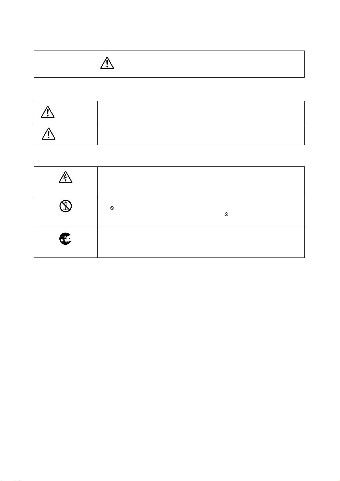
SERVICE SAFETY PRECAUTIONS
• The caution items shown here describe major safety issues and should always be observed.
• The meanings of the various indications are as follows.
WARNING
CAUTION
* Physical damage means major damage to a home, furnishings and other possessions.
Examples of marks
SHOCK HAZARD
PROHIBIT DISASSEM-
BLING
UNPULUG
Indicates a hypothetical situation in which service personnel and nearby third parties, or even
end users due to a product defect after the service operation is completed, could possibly be in
danger of injury or even death in the event of operational error.
Indicates a hypothetical situation in which service personnel and nearby third parties, or even
end users after the service operation is completed, could possibly be in danger of injury, or
where there could be physical damage in the event of operational error.
The" indicates caution (including danger and warning).
"
The actual meaning of this caution is indicated inside the
The example shown to the left indicates the danger of "electrical shock".
indicates a forbidden action.
The
The actual meaning of this caution is indicated inside the
The example shown to the left indicates that disassembly is forbidden.
The
-
indicates a forced action (an action that must be performed).
The actual meaning of this forced action is indicated by
The example shown to the left indicates that the power plug must be disconnected.
or nearby illustrations or text.
or nearby illustrations or text.
-
or nearby illustrations or text.
-
3
-
Page 4
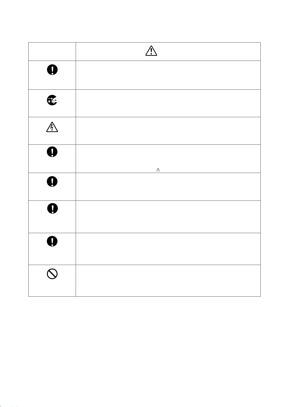
KEEP CHILDREN
AWAY
UNPULUG
SHOCK HAZARD
USE SPECIFIED
PARTS
CAUTION FOR
WIRING
CAUTION FOR
ASSEMBLING /
WIRING
WARNING
• Always advise users to keep children away.
There is danger of injury to children from tools, disassembled products, etc.
• Always disconnect the power plug before starting work whenever power is not required.
Failure to disconnect the power plug before starting work can result in electrical shock.
• Depending on the model, use an insulation transformer or wear gloves when servicing with the
power on, and disconnect the power plug to avoid electrical shock when replacing parts.
In some cases, alternating current is also impressed in the chassis, so electrical shock is possible if the chassis is contacted with the power on.
• Always use the replacement parts specified for the particular model when making repairs.
The parts used in products have the necessary safety characteristics such as inflammability,
voltage resistance, etc.; therefore, use only replacement parts that have these same characteristics.
Use only the specified parts when the
• Parts mounting and routing of the wiring should be the same as that used originally.
For safety purposes, insulating materials such as tubing or tape is sometimes used and printed
circuit boards are sometimes mounted floating.
Also make sure that wiring is routed and clamped to avoid parts that generate heat and which
use high voltage. Always follow the original scheme.
• After a repair has been completed, reassemble all disassembled parts, and route and reconnect the wiring, in accordance with the original scheme.
Do not allow internal wiring to be pinched by cabinets, panels, etc.
Any error in reassembly or wiring can result in electrical leakage, flame, etc., and may be
hazardous.
mark is included in a circuit diagram or parts list.
CHECK INSULATION
RESISTANCE
PROHIBIT
REMODELING
• After completing the work, disconnect the power plug from the outlet, remove the antenna, turn
on the power switch. Then, use a 500V insulation resistance meter to check the insulation
resistance of the antenna terminal, other metallic parts and between the prongs of the power
plug to make sure that the insulation resistance is 1M 1 or more.
The set will require inspection and repair if the insulation resistance is below this value.
• Never remodel the product in any way.
Remodeling can result in improper operation, malfunction, or electrical leakage and flame,
which may be hazardous
-
4
-
Page 5
HANDLING THE LCD MODULE
a
n
r
r
y
n
r
e
h
d
-
Safety Precautions
In the event that the screen is damaged or the liquid crystal
(fluid) leaks, do not breathe in or drink this fluid. Also, never
touch this fluid.
Such actions could cause toxicity or skin irritation. If this fluid
should enter the mouth, rinse the mouth thoroughly with water. If the fluid should contact the skin or clothing, wipe off
with alcohol, etc., and rinse thoroughly with water. If the fluid
should enter the eyes, immediately rinse the eyes thoroughly
with running water.
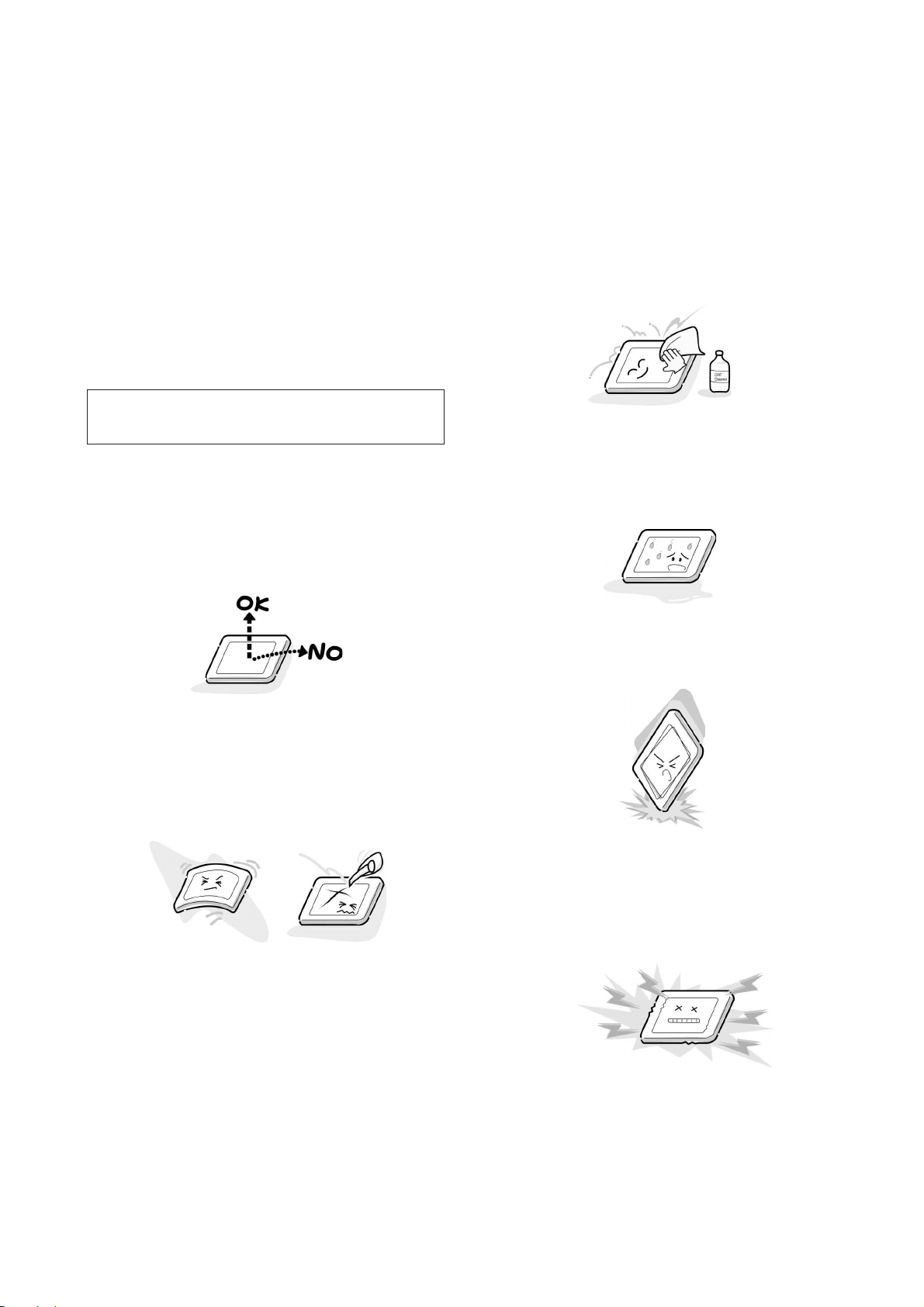
Precautions for Handling the LCD Module
CAUTION
The LCD module can easily be damaged during disassembly
or reassembly; therefore, always observe the following precautions when handling the module.
1. When attaching the LCD module to the LCD cover, position it appropriately and fasten at the position where the
display can be viewed most conveniently.
The metal edges of the LCD module
are sharp, handle it with care.
3. If the panel surface becomes soiled, wipe with cotton or
soft cloth. If this does not remove the soiling, breathe o
the surface and then wipe again.
If the panel surface is extremely solied, use a CRT cleane
as a cleaner. Wipe off the panel surface by drop the cleane
on the cloth. Do not drop the cleaner on the panel. Pa
attention not to scratch the panel surface.
4. Leaving water or other fluids on the panel screen for a
extended period of time can result in discoloration o
stripes. Immediately remove any type of fluid from th
screen.
2. Carefully align the holes at all four corners of the LCD
module with the corresponding holes in the LCD cover
and fasten with screws. Do not strongly push on the module because any impact can adversely affect the performance. Also use caution when handling the polarized screen
because it can easily be damaged.
5. Glass is used in the panel, so do not drop or strike wit
hard objects. Such actions can damage the panel.
6. CMOS-LSI circuitry is used in the LCD module, so avoi
damage due to static electricity. When handling the mod
ule, use a wrist ground or anchor ground.
-
5
-
Page 6
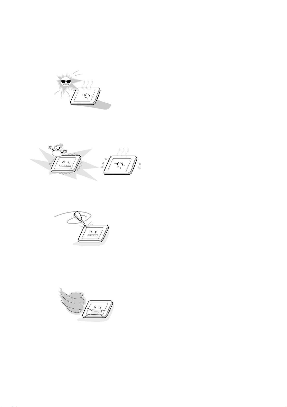
7. Do not expose the LCD module to direct sunlight or strong
ultraviolet rays for an extended period of time.
8. Do not store the LCD module below the temperature conditions described in the specifications. Failure to do so
could result in freezing of the liquid crystal due to cold air
or loss of resilience or other damage.
9. Do not disassemble the LCD module. Such actions could
result in improper operation.
10. When transporting the LCD module, do not use packing
containing epoxy resin (amine) or silicon resin (alcohol or
oxim). The gas generated by these materials can cause
loss of polarity.
-
6
-
Page 7
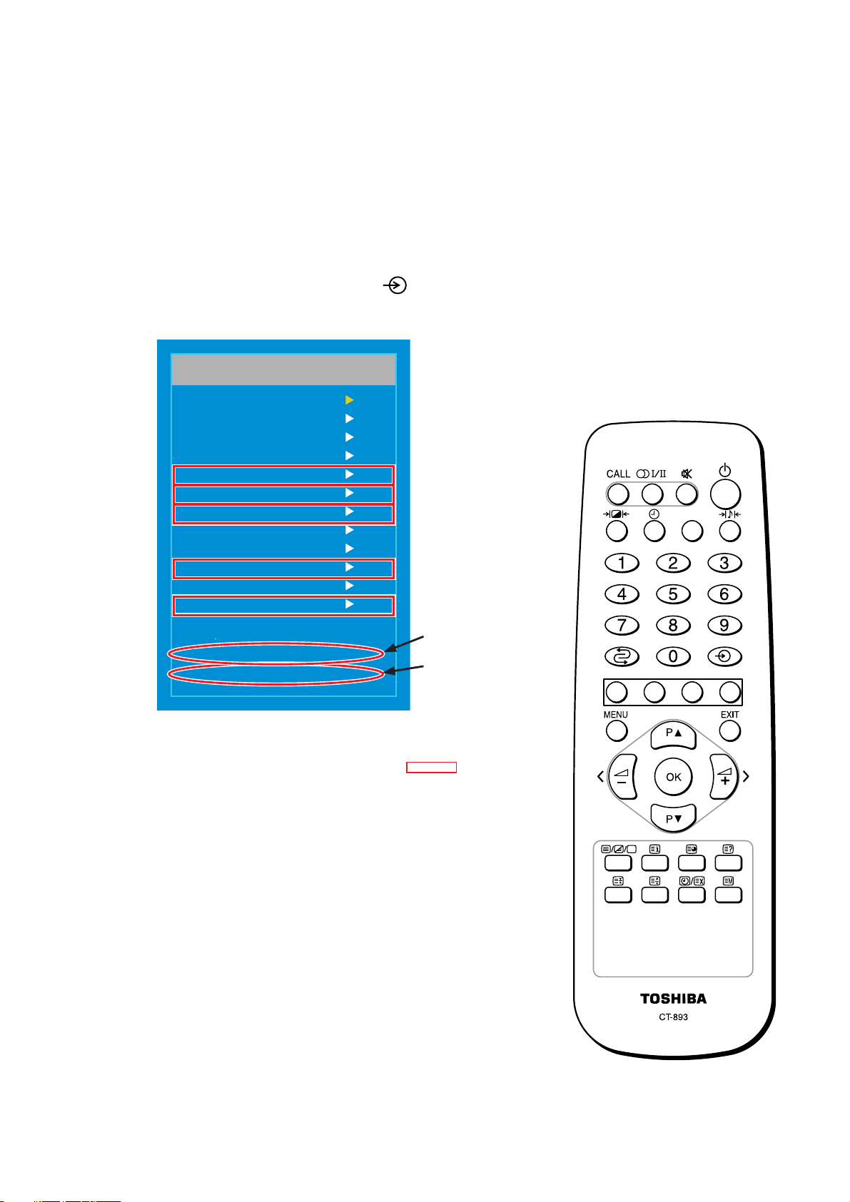
1.Service Mode
1-1.Starting Service Mode
*Set LCD TV to the normal TV signal receive mode.
Note: In this "Service Mode" section, [ ] shows a button.
1-1-1. Press [MUTE] on the remote control once.
1-1-2. Press [MUTE] again, and press [
Service Menu
Scaler ADCScaler ADC
9883ADC
VCTIADC
Audio
Option 1
Option 2
Option 3
DRX Set
NVM Edit
Download
Reset TV
Hotel Mode
FrequencyFrequency 47054705
Gm2221Gm2221 Ver. 3. 22.Ver. 3. 22.
VCTiVCTi Ver. 3. 49.Ver. 3. 49.
] on LCD TV.
Scaler version
VCTi version
Service mode displayed on TV screen
Items other than those enclosed by are default
settings.
*For EU,Hotel mode setting is not a vailable.
-
7
-
Page 8
OPTION DEFAULT DATA
15VL56B
Option 1 15VL56B
SAV 1
SCART 1
PC 1
Side Comp 0
16:9 0
200 PR 0
Te xt 1
ACMS 1
Option 2 15VL56B
HiDev 0
Hotel 0
To p 1
I ll SAVE 0
Turbo Vol 0
Ch/Aus 0
Option 3 15VL56B
Language 0
Txt Lang 7
Inch opt 2
PA NE L 0
20VL56B/G
Option 1 20VL56B 20VL56G
SAV 1 1
SCART 1 1
PC 1 1
Side Comp 0 0
16:9 0 0
200 PR 0 0
Te xt 1 1
ACMS 1 1
Option 2 20VL56B 20VL56G
HiDev 0 0
Hotel 0 0
To p 1 1
I ll SAVE 0 0
Turbo Vol 0 0
Ch/Aus 0 0
Option 3 20VL56B 20VL56G
Language 0 0
Txt Lang 7 7
Inch opt 3 3
PA NE L 0 0
-
8
-
Page 9

2. Adjustment
Note: In this "Adjustment" section, [ ] shows a button.
2-1.Adjustment Tools and Conditions
Tools: Pattern Generator (801GF, MSPG925F)
DDC Adjustment Tool
PC
Remote Control
Conditions: Heat Run 30 minutes or more
2-2. Auto Gain/Offset Adjustment
2-2-1. RF Mode Adjustment (normal TV receive mode)
No reguired
2-2-2. Component Mode Adjustment
Preparation
Carry out Heat Run for 30 minutes or more before
adjustment (with no RF signal).
1) Connect Y, Pb, and Pr output signals of Pattern Generator
to the component jack (Y, Pb, Pr) of LCD TV.
2) Connect Y, Pb, and Pr output signals of Pattern
Generator to the component jack (D Jack) of LCD TV.
3) Change the TV input mode to component mode.
4) Select 480p Mode (Y:100% Pb/Pr:75%) in Pattern Generator. Select Pattern 33 (Color Bar
Pattern signal) in Pattern Generator (MSPG925F).
5) Go into service mode, and Auto Gain menu appears, and then press VOL [+].
6) Press [OK] to store the adjustment data.
(Adjustment in component mode or PC mode)
2-2-3. PC Mode Adjustment
Preparation
Carry out Heat Run for 30 minutes or more before adjustment (with no RF signal).
Connect Pattern Generator to the 15-pin D-Sub Jack of LCD TV.
1) Change the TV input mode to PC mode.
2) Set Pattern Generator to the following:
15VL56B : XGA (1024x768) 16-step or 11-step grayscale
20VL56B,20VL56G : VGA (640x480) 16-step grayscale
3) Go into service mode, and Auto Gain menu appears, and then press VOL [+].
4) Press [OK] to store the adjustment data.
-
9
-
Page 10

2-3. DDC EDID Data Read & Write
The following software programs are used to read/write DDC EDID data.
DLPortIO.exe
t15.edi
t20.edi
UserPort.exe
UserPort.sys
WinEDID_2.0.exe
Be very careful that DDC EDID data read/write varies depending on Operating System conditions
of PC.
(See the fl owchart below.)
(Windows/system32/Drivers)
J
Start
OS: MS Windows 2000, XP
Port Setup: (2-3-1)
Preparation EDID Reading & Writing: (2-3-2)
Confi rmation of Updated EDID Data: (2-3-5)
OS: MS Windows 98
EDID Read: (2-3-3)
EDID Write: (2-3-4)
-
10
-
Page 11
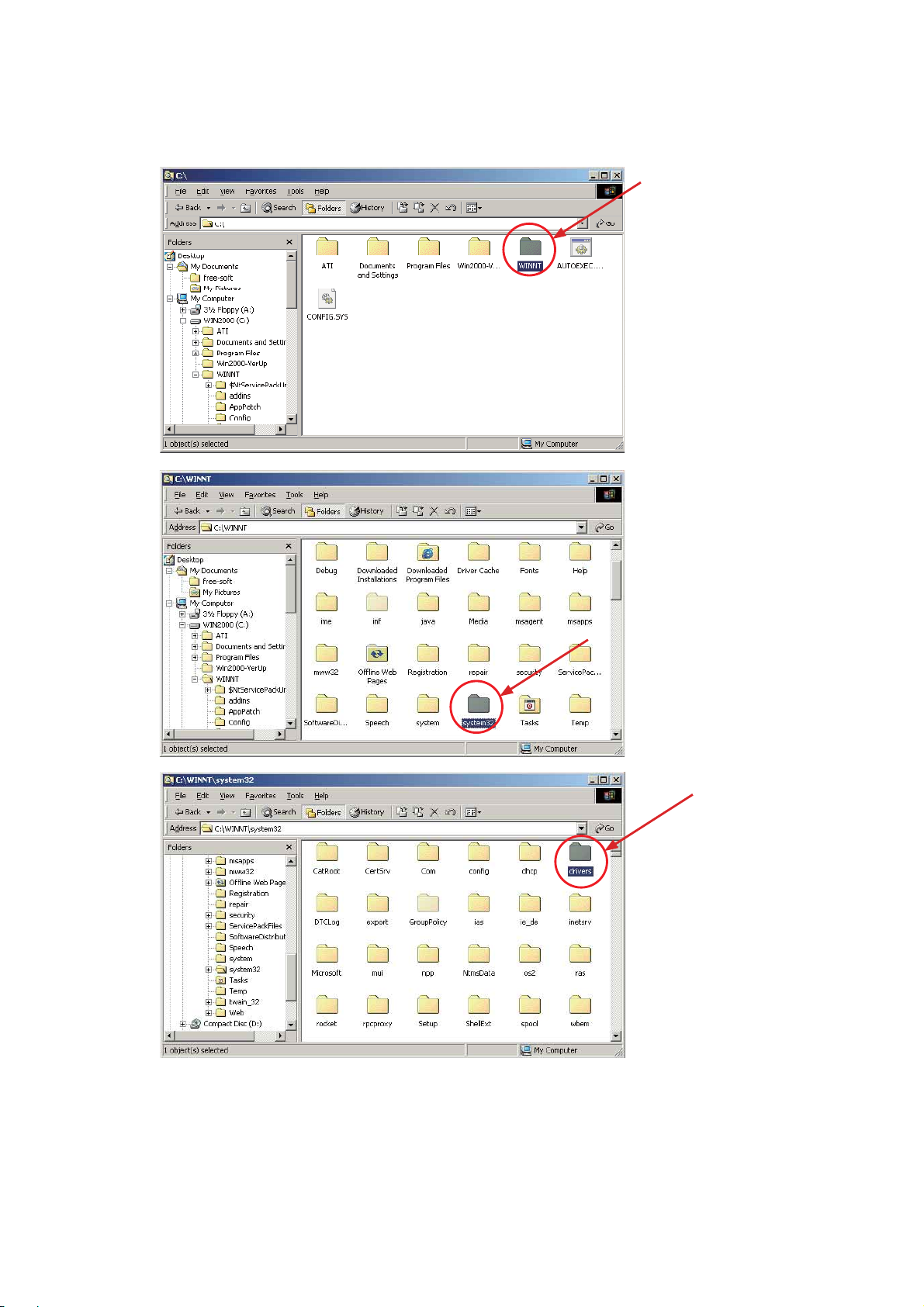
2-3-1. Port Setup (Windows 2000, XP only)
1) Copy "UserPort.sys" fi le to c:\windows\system32\drivers.
-
11
-
Page 12

2) Double-click "DLPortIO.exe" to install port setting program.
Double-click "DLPortIO.exe"
3) When the port setting program starts up, the installation program runs automatically. Continue
the installation by following instructions on the window.
Click "Next" to continue
the installation.
Click "Yes" to continue
the installation.
4) Select "Typical" on the Setup Type window and click "Next" to continue.
Select "Typical" and click
"Next" to continue.
Click "Next" to continue.
-
12
-
Page 13
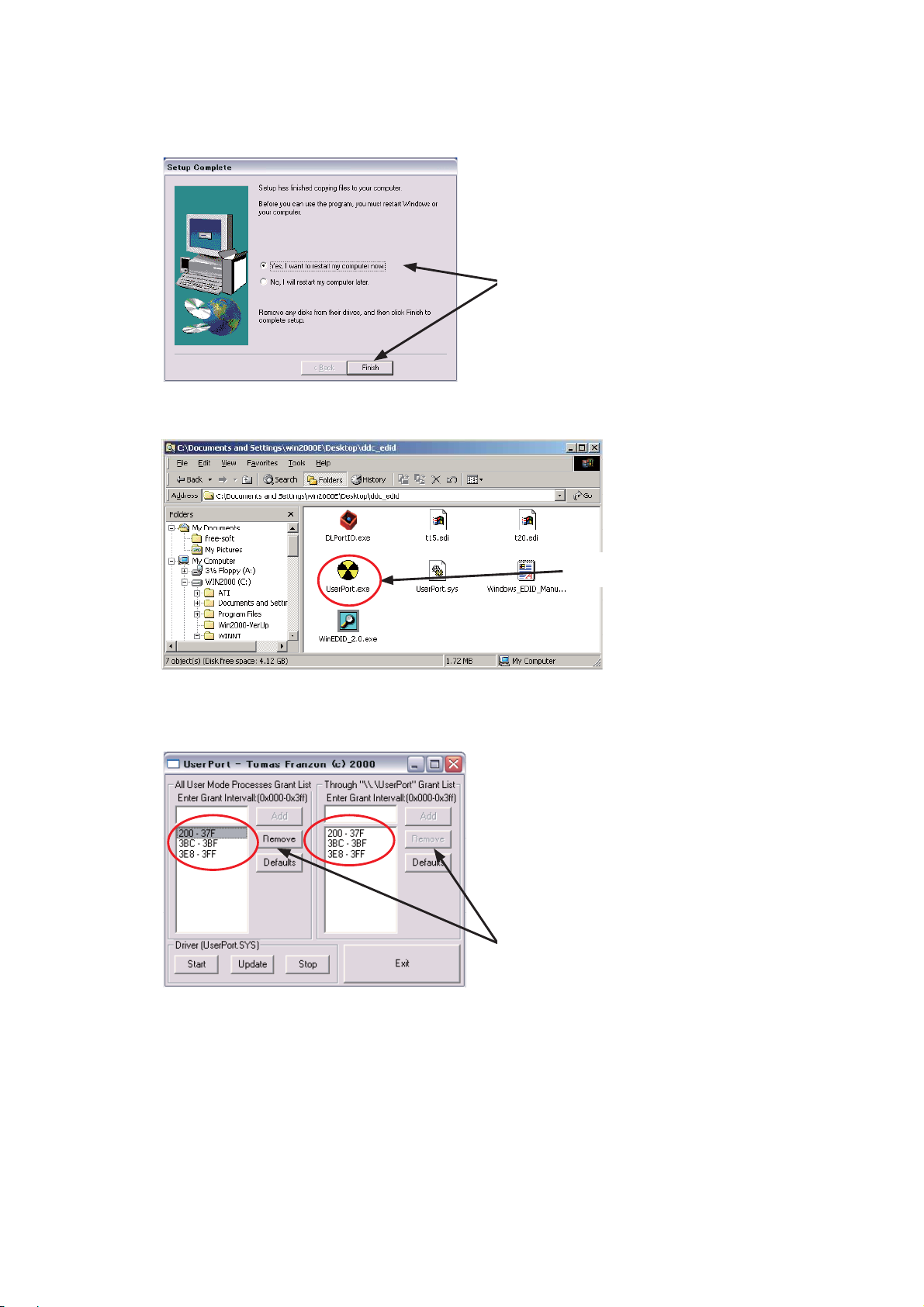
5) Select "Yes, I want to restart.." for PC restart and click "Finish" to complete the installation.
Select "Yes, I want to restart.." and click
"Finish" to complete the installation.
6) Double-click "UserPort.exe" to begin the installation.
Double-click "UserPort.exe".
7) Click the numbers in the red circle on the UserPort window, and click "Remove" to remove all
default numbers.
Click "Remove" to remove all default numbers.
-
13
-
Page 14
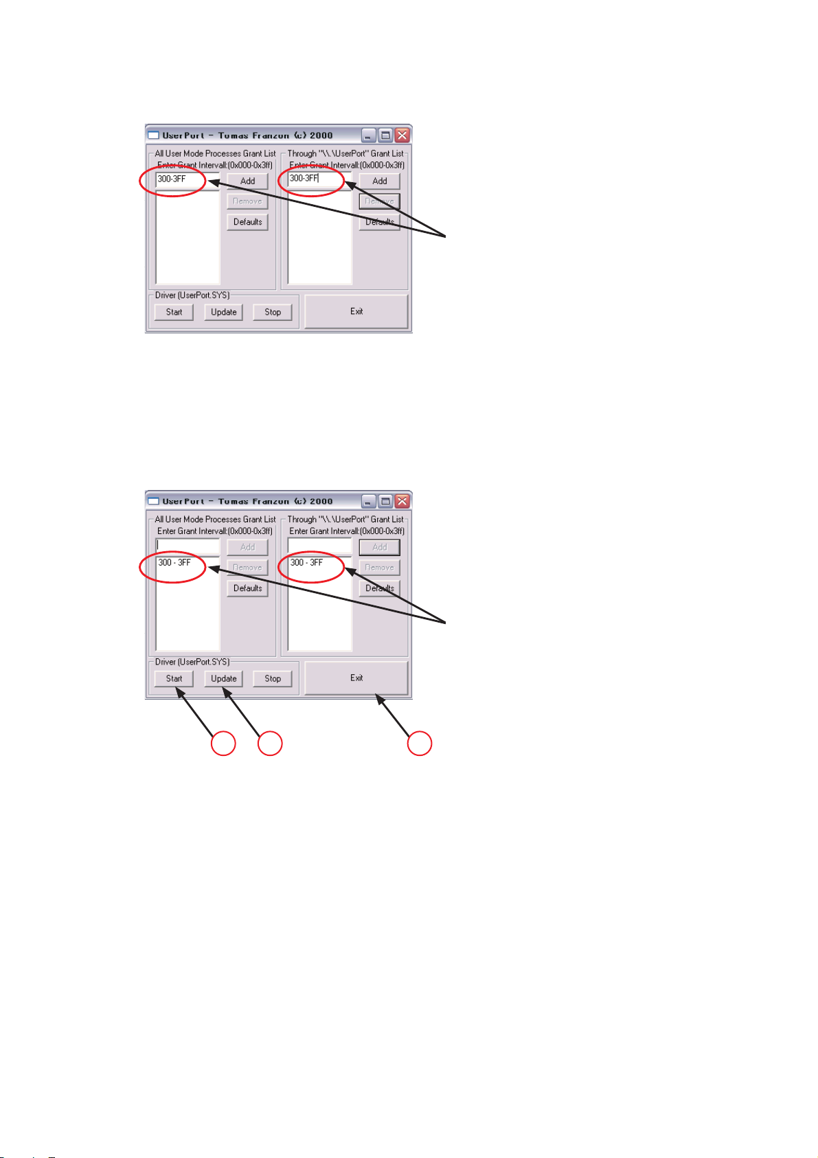
8) Add data value "300-3FF" to two areas on the UserPort window and click "Add".
After key in Value "300-3FF", click [Add]
to store "300-3FF".
9) Confi rm that "300-3FF" is added on the UserPort window. Then update the driver using the
following procedure.
1
Click [Update].
2
Click [Start].
3
Click [Exit] to fi nish the setup.
2 1 3
Added Value "300-3FF" appears.
-
14
-
Page 15
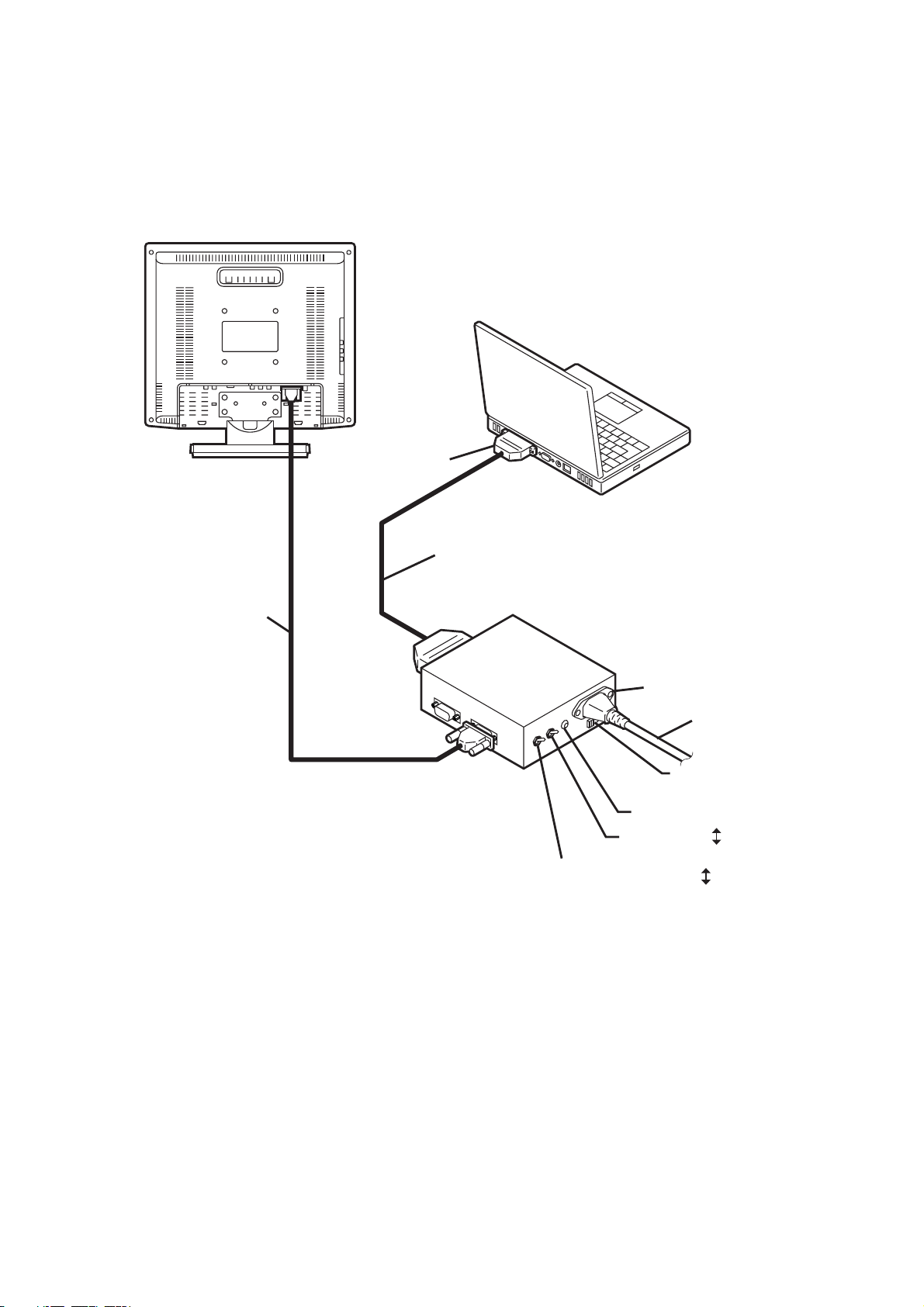
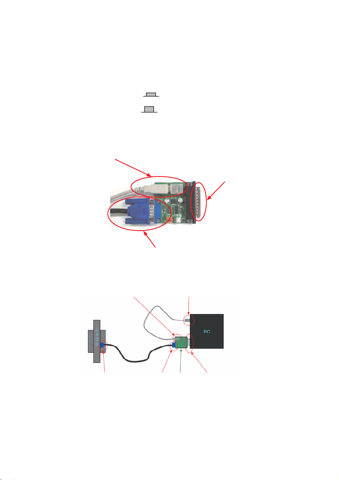
2-3-2. Preparation EDID Reading & Writing
Connect the LCD TV and PC using DDC Jig. (See the fi gure below.)
After connection is completed, turn the power ON of the LCD TV.
LCD TV
Parallel Port
PC
Parallel Port Cable
D-SUB Cable
DDC
ADAPTER
Monitor
Jig
Power inlet
Power LED
ST switch
V-Sync On/Off switch
(Switch must be ON.)
Power cord
Power select switch
ON
(
)
OFF
ON
(
)
OFF
-
15
-
Page 16
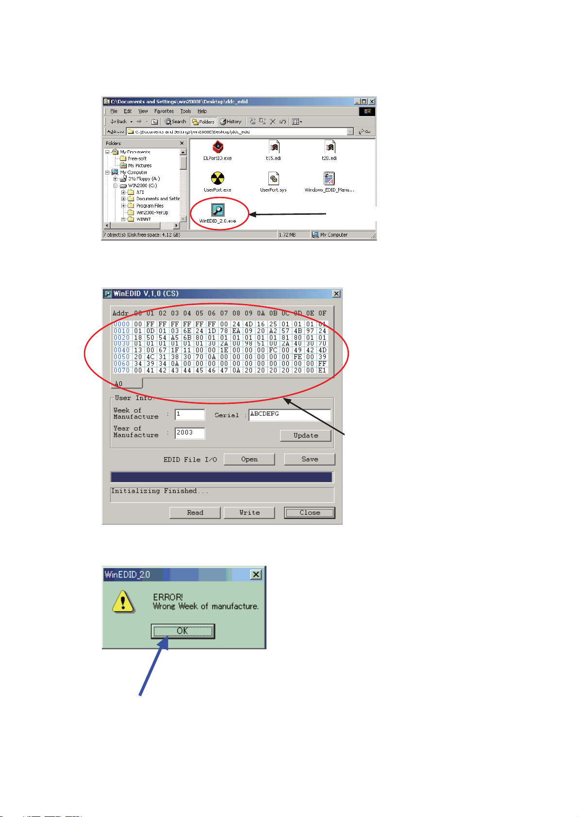
2-3-3. EDID Reading
1) Double-click "WinEDID.exe" to read EDID data.
Double-click "WinEDID.exe".
2) The WinEDID window opens. The program might read the current EDID data automatically.
Current EDID data might be displayed on
the WinEDID window.
Ignore this error message appearing several times by clicking OK.
-
16
-
Page 17
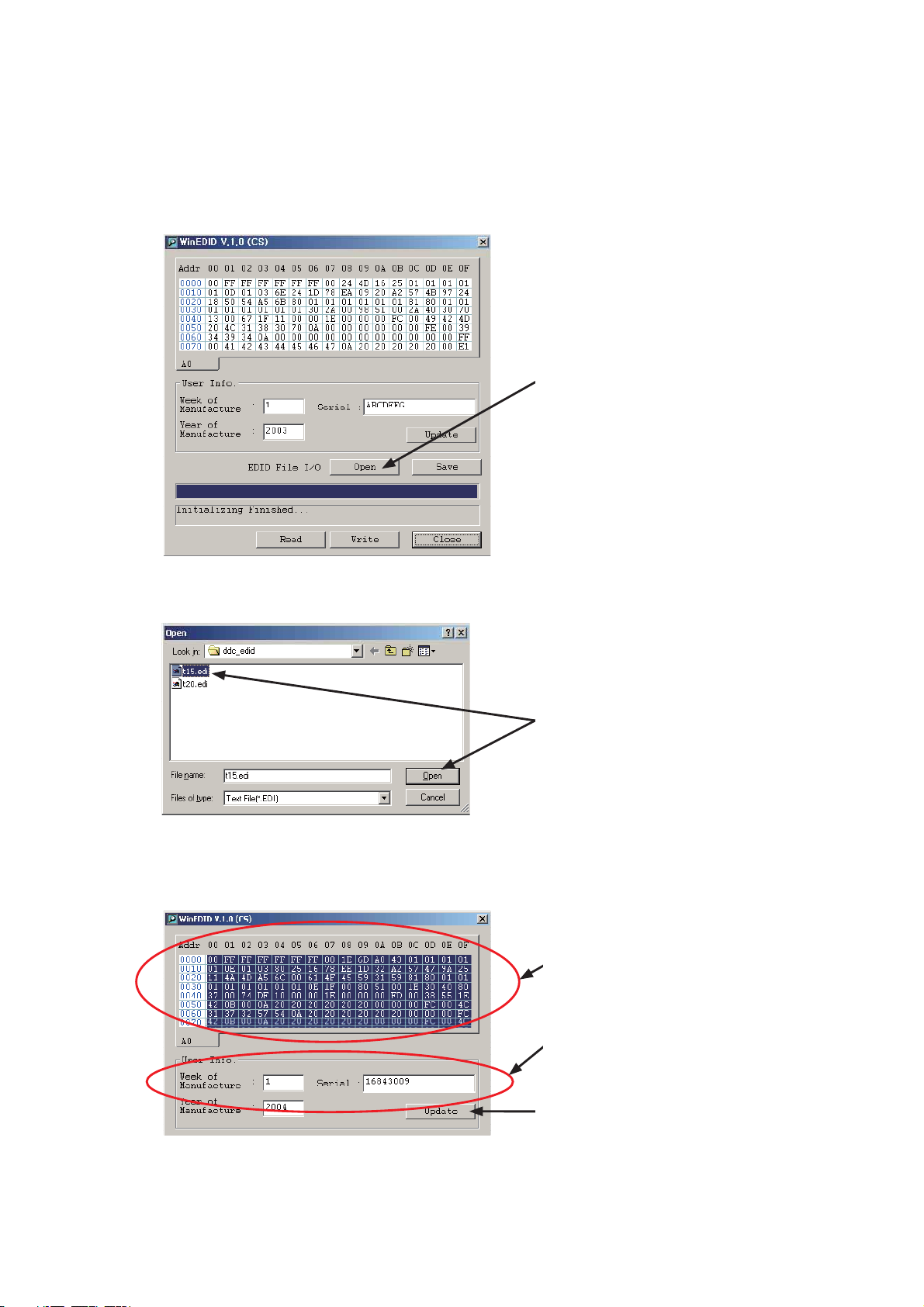
2-3-4. EDID Writing
1) Click [Open] on the WinEDID window, and search for EDIC fi le(*.edi) that matches TV size.
t15.edi : 15VL56B
t20.edi : 20VL56B,20VL56G
Click [Open]
2) When the fi le is found, click the fi le to open.
Select EDIC fi le(*.edi) that matches TV size
and click [Open]
3) The content of selected EDID fi le is displayed on the WinEDID window. Click [Update].
Note: Do not change any data appeared in User Info.
Content of selected EDID fi le
Do not change
-
17
Click [Update]
-
Page 18
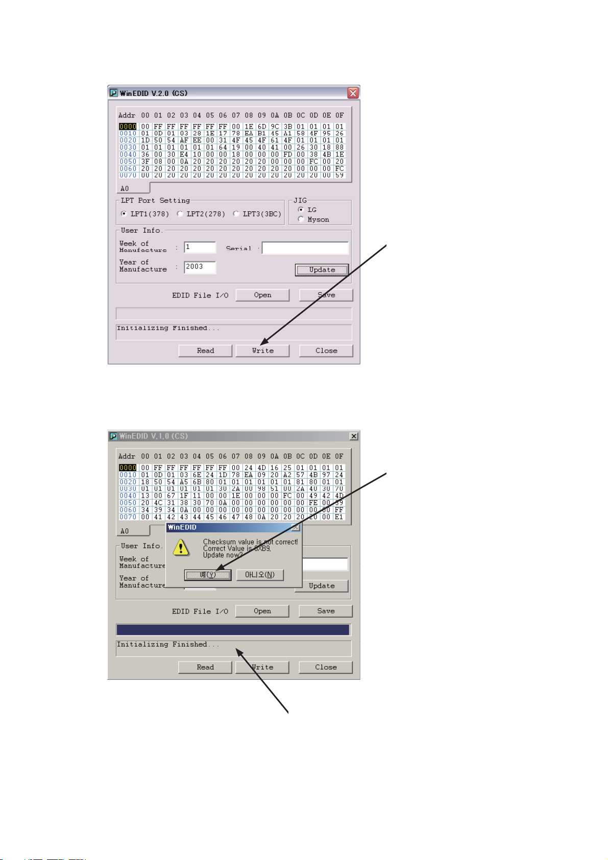
4) Click [Write] on the WinEDID window to update EDID data.
Click [Write]
5) When checksum error message appears, ignore this error and click [Y]. Upon writing process
completed, "Write Data ....Finished" message will appear.
Click [Y]
Upon writing process completed, "Write Data
....Finished" message will appear.
-
18
-
Page 19
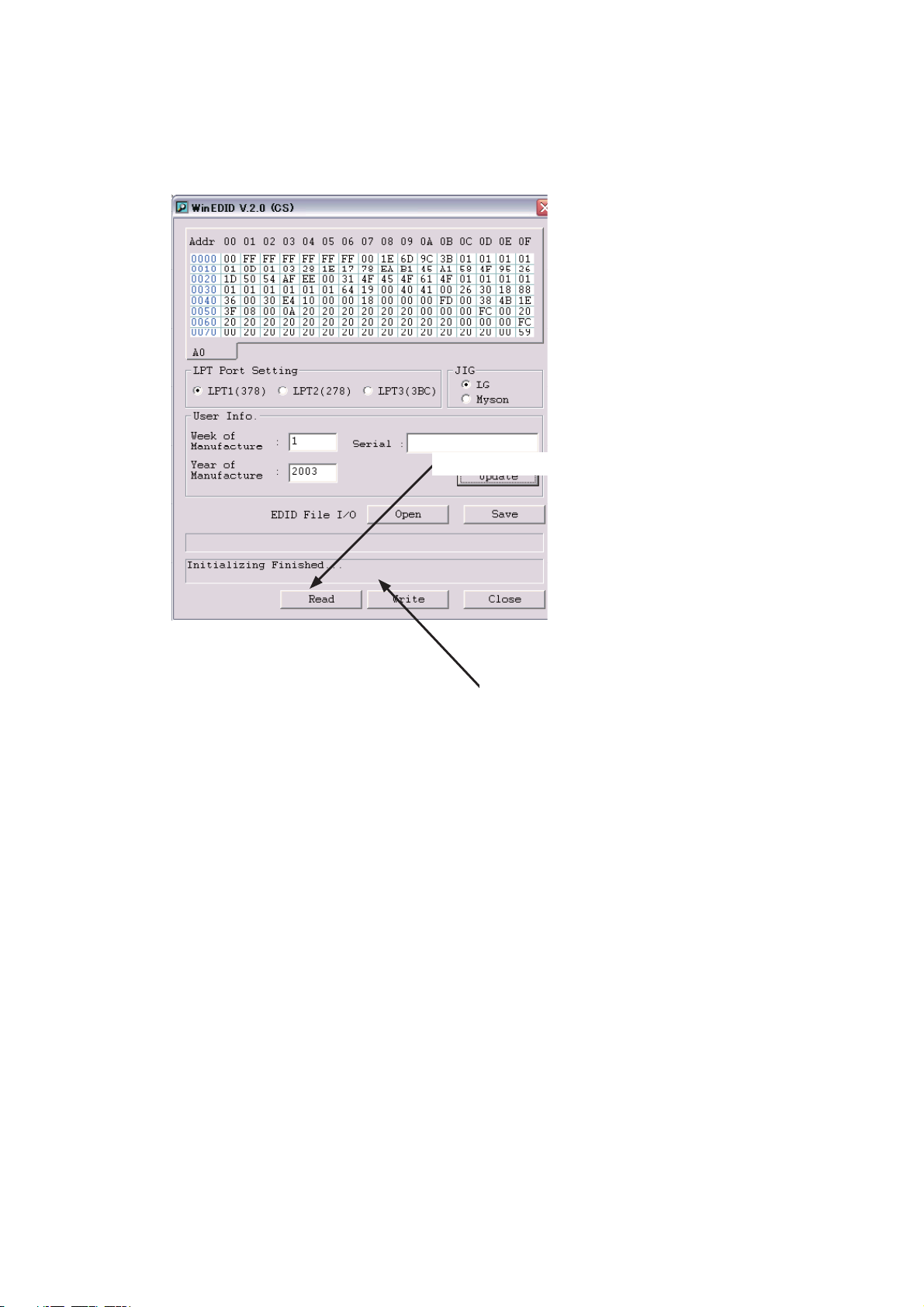
2-3-5. Confi rmation of Updated EDID Data
Click [Read] to confi rm that the EDID data are written as copied from original data.
Click [Read]
Upon reading process completed, "Read Data
....Finished" message will appear.
-
19
-
Page 20
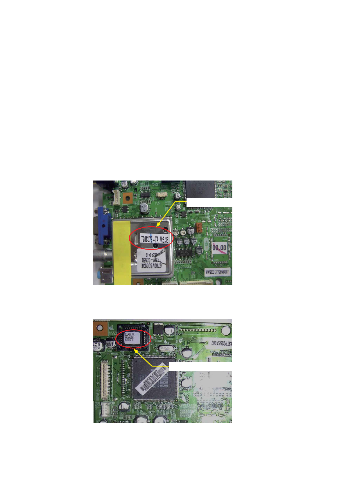
3. VCTi Firmware Installation/Upgrading
This LCD TV uses two fi rmware programs.
1. VCTi fi rmware
2. SCALER fi rmware
When the main board or IC200 is replaced, be sure to install the VCTi49xxY firmware. (No
program is included in the IC200 spare parts.)
This fi rmware program must also be installed when a new fi rmware upgrade fi le is supplied to
improve the performance.
Note: In this "VCTi Firmware Installation/Upgrading" section, [ ] show a clicking point on installation
menu.
Firmware version indication
VCTi fi rmware version
Scaler Firmware indication
SCALER fi rmware version
-
20
-
Page 21
3-1. VCTi Firmware Installation
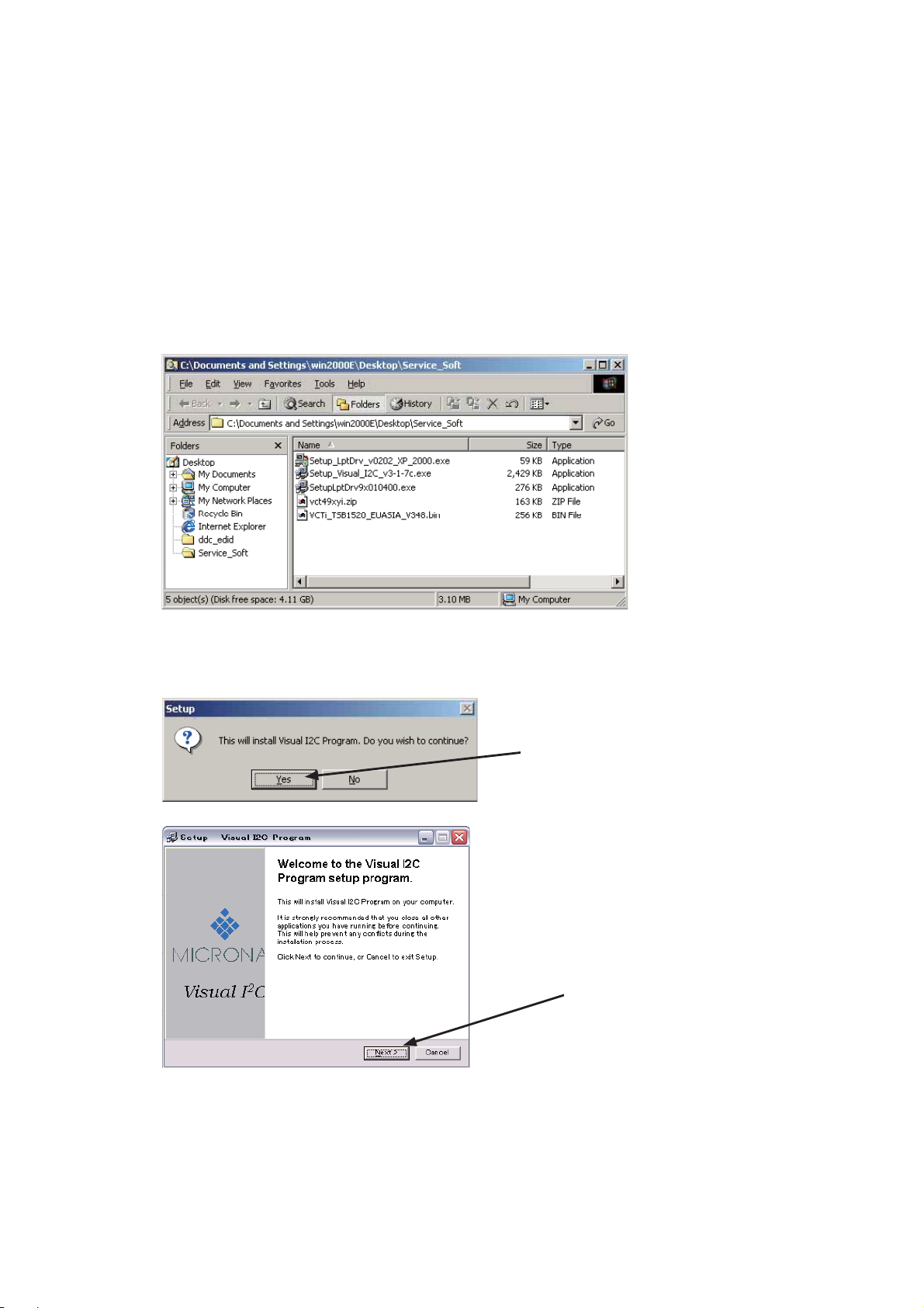
3-1-1. Preparation
1) Create a new folder on PC and copy the following fi les to the folder.
VCTi_TSBxxx_xxx_Vxxx.bin (Vxxx shows fi rmware version.)
vct49xyi.zip
Setup_Visual_I2C_v3xxx.exe
SetupLptDrv9x010400.exe
Setup_LptDrv_v0202_XP_2000.exe
Note: These software programs are supplied as required.
2) Double-click Setup_Visual_I2C_v3xxx.exe.
Continue the installation by following instructions on the window. Click [Finish] at the last to
complete the installation.
Click [Yes]
Click [Next] on the Visual I2C Program
installation window.
-
21
-
Page 22

3) Select appropriate driver fi le according to your PC OS.
Windows 98 : SetupLptDrv9x010400.exe
Windows 2000/XP : Setup_LptDrv_v0202_XP_2000.exe
Double-click the fi le appropriate for your PC OS. The following window opens.
Click [I Agree] on the installation window to complete the driver installation.
Click [I Agree] to complete the driver
installation.
4) Unzip "vct49xyi.zip" fi le.
After unzipping, "vct49xyi.zip" folder will be created.
Unzip "vct49xyi.zip" fi le to create
"vct49xyi.zip" folder.
Installation of software programs necessary for "VCTi Firmware Installation/Upgrading" in PC has
been completed.
-
22
-
Page 23
3-1-2. Proceeding VCTi Firmware Upgrading
Preparation: Connect PC and TV using Jig before proceeding.
1
Disconnect AC power cord of TV.
2
Connect Jig to PC connector on TV with D-sub cable.
3
Connect USB connector on Jig to USB connector on PC.
4
Connect LPT port of Jig to LPT port of PC.
5
Press the Jig switch down. ( )
6
Plug the AC power cord to go into standby mode. (The LED lights up red.)
7
Press the Jig switch again. ( )
Connect USB cable connector
(small).
Connect USB cable connector (small)
to USB connector on Jig board.
Connect directly to D-sub 25 pin
connector on PC.
Connect one D-sub 9 pin cable
connector.
Connect USB cable connector (large)
to USB connector on PC.
Connect one D-sub 9 pin cable
connector to PC connector on
TV.
Connect the other
D-sub 9 pin cable
connector to D-sub 9
pin connector on Jig
board.
-
23
Vcti Jig
board
-
Connect D-sub 25 pin connector
on Jig board directly to D-sub 25
pin connector on PC.
Page 24

1) Double-click "vcth_tvt.vi2c" fi le in "vct49xyi" folder to install the fi rmware.
Double-click "vcth_tvt.vi2c" fi le.
2) An error message appears. Ignore this message. Click [OK] to continue installation.
Click [OK]
3) The following window appears. Double-click the fi le name next to [Load Bin -> Flash].
Double-click this fi le name
4) The following window appears. Click the button (
…
) at the right end of "Name" to open the
fi le select window.
Click … button
-
24
-
Page 25

5) Select VCTi_TSBxxx_xxx_Vxxx.bin copied in 3-1-1 and click [Open].
6) Confi rm that the selected fi le is displayed in "Name" on the Watch Item… window.
Necessary fi rmware has been appeared. Click [OK].
Click [OK]
7) Set printer (LPT) on the vcth_txt_vi2c window.
Select "File" – "Preferences" – "LPT Preferences…" to open the LPT Setting window.
Set LPT1 for LPT Port and 8 for Delay, and click [OK].
Set LPT1
Set 8
Click [OK]
-
25
-
Page 26

8) Click cross box mark X till 21 or 22 appears.
If 21 or 22 does not appear, TV may not be in the fi rmware installation mode. Unplug the AC
power cord of TV and repeat steps from 3-1-2 "Preparation".
9) Click [Erase Flash] to erase fl ash memory data.
10) Click [Load Bin -> Flash] to start installation of the fi rmware.
Note: Progress window appears and wait till 100% completed.
8)
9)
10)
11) Press the Jig switch down. ( )
12) Disconnect the cable from PC connector on TV.
13) Unplug the AC power cord, and plug it again and turn ON the power of TV.
3-1-3. Confi rmation after Installation of VCTi Firmware
Go into service mode to check that the VCTi fi rmware version is upgraded.
Service Menu
Scaler ADCScaler ADC
9883ADC
VCTIADC
Audio
Option 1
Option 2
Option 3
DRX Set
NVM Edit
Download
Reset TV
Hotel Mode
Upgraded VCTi fi rmware version
FrequencyFrequency 47054705
Gm2221Gm2221 Ver. 3. 22.Ver. 3. 22.
VCTiVCTi Ver. 3. 49.Ver. 3. 49.
-
26
-
Page 27

3-2. SCALER Firmware Installation
3-2-1. Preparation
1) Create a new folder on PC and copy the following fi les to the folder.
CGProbe Redistributable 5.1.0.5.exe
ISPUtility 1.0.0.6.exe
Toshiba_15(SCALER)_Verx.xx.hex I (for 15-inch TV)
Toshiba_20(SCALER)_Verx.xx.hex I (for 20-inch TV)
Note: These software programs are supplied as required.
2) Double-click "CGProbe Redistributable 5.1.0.5.exe" to start installation of Genesis CGprobe
Library 5.
Continue the installation following instructions on the window.
Select "I accept the agreement" and
click [Next]
Click [Next]
3) Click [Finish] last to complete the installation. Upon completion of installation, the "DLPortIO"
folder is created in C: \Program Files to store necessary fi les.
Click [Finish] to complete the installation
-
27
-
Page 28

4) Double-click "ISPUtility1.0.0.6.exe" to start installation of Genesis ISP Utility1.
Continue the installation following instructions on the window.
Double-click this to start installation
Select "I accept the agreement" and
click [Next]
Click [Next]
5) Click [Next] to continue the installation.
Click [Next] Click [Next]
6) Select the "create a desktop icon" checkbox on the installation window, and click [Next] to
continue the installation. Click [Finish] last to complete the installation. (ISP Utility icon will be
created on the desk top.)
Click [Next] Click [Finish] to complete the installation
Installation of necessary software programs for "SCALER Firmware Installation" in PC has been
completed.
-
28
-
Page 29

3-2-2. Proceeding SCALER Firmware upgrading
Preparation: Connect PC and TV using Jig before proceeding.
1
Disconnect AC power cord of TV.
2
Connect Jig to PC connector on TV with D-sub cable.
3
Connect USB connector on Jig to USB connector on PC.
4
Connect D-sub 9 pin connector on Jig to D-sub 9 pin connector on PC.
5
Plug the AC power cord to go into standby mode. (The LED lights up red.)
Connect USB connector on Jig to
USB connector on PC
Connect to D-sub 9 pin
connector on PC
Connect PC connector on Jig
to PC connector on TV with
D-sub cable
Connect USB connector on Jig to
USB connector on PC
Connect PC connector on Jig to
PC connector on TV with D-sub
cable
Connect to D-sub 9 pin
connector on PC
-
29
-
Page 30

1) Double-click "ISP Utility" icon created on the desktop to run the Genesis ISP Utility program.
2) Set "connection" in ISP Settings to "Serial" on the Genesis ISP Utility window.
Click [T] to select "Serial"
3) Set "Chip" in ISP Settings to "GM5221BC" on the Genesis ISP Utility window.
Click [T] to select "GM5221BC"
4) Set "Flash" in ISP Settings to "SST39F010" on the Genesis ISP Utility window.
Check all settings and click [Settings].
Click [T] to select "SST39F010"
Check all settings and click [Settings].
The Connection Settings window appears.
-
30
-
Page 31

5) Set all the settings on the Connection Settings window to those in the table below. Check
all the settings, and then click [OK].
6) Click [
Item Setting
Port COM1
Baud Rate 115200
Datat Bits 8
Parity None
Stop Bits 1
Read Interva 0
Read Multiplier 0
Read Constant 0
Write Multiplier 0
Write Constant 0
Scheme Default Serial Profi le
Click [OK]
] on the Genesis ISP Utility window to load necessary "hex" data fi le.
Click [] to load necessary "hex" data fi le.
Click [OPEN] to load necessary "hex" data fi le.
7) Check that the necessary "hex" data fi le name is displayed in Flash Image on the Genesis
ISP Utility window. Setup of the SCALER fi rmware upgrading is completed.
Check that the "hex" data fi le has been loaded
-
31
-
Page 32

3-2-3. SCALER Firmware Upgrading
1) Set TV to service mode.
Starting Service Mode
1
Volume indication appears on the TV screen. Press [ ] on TV when the Volume indication
2) The Service Mode window appears on the TV screen. Check the SCALER fi rmware version
Press [MUTE] on the remote control once.
2
Keep pressing [MUTE] again.
disappears.
before upgrade.
Service Menu
Scaler ADCScaler ADC
9883ADC
VCTIADC
Audio
Option 1
Option 2
Option 3
DRX Set
NVM Edit
Download
Reset TV
Hotel Mode
FrequencyFrequency 47054705
Gm2221Gm2221 Ver. 3. 22.Ver. 3. 22.
VCTiVCTi Ver. 3. 49.Ver. 3. 49.
SCALER fi rmware version before upgrade
3) Move the cursor to "Download" with CH [T] on the remote control. Then press VOL [+] to
perform "Download".
Service Menu
Scaler ADCScaler ADC
9883ADC
VCTIADC
Audio
Option 1
Option 2
Option 3
DRX Set
NVM Edit
Download
Reset TV
Hotel Mode
FrequencyFrequency 47054705
Gm2221Gm2221 Ver. 3. 22.Ver. 3. 22.
VCTiVCTi Ver. 3. 49.Ver. 3. 49.
Remote control
CH [T] : Select "Download" item
VOL [+] : Perform "Download"
4) The SCALER DOWNLOAD window appears on the TV screen, and the TV becomes download
standby mode.
-
32
-
Page 33

5) Click [Start] on the Genesis ISP Utility window of PC to start installing new SCALER fi rmware.
Click [Start] to install new
SCALER fi rmware
6) Check that the new SCALER fi rmware has been installed.
Upon completion of the installation, "ISP
successful" appears in "Status" of Run ISP
7) Unplug the AC power cord from TV. Wait for about 5 seconds and connect the AC power cord
again.
3-2-4. Checking after Upgrading of SCALER Firmware.
et TV to service mo
S
The TV goes into service mode. Check that the SCALER fi rmware version is upgraded.
Service Menu
Scaler ADCScaler ADC
9883ADC
VCTIADC
Audio
Option 1
Option 2
Option 3
DRX Set
NVM Edit
Download
Reset TV
Hotel Mode
FrequencyFrequency 47054705
Gm2221Gm2221 Ver. 3. 22.Ver. 3. 22.
VCTiVCTi Ver. 3. 49.Ver. 3. 49.
de.
Upgraded SCALER fi rmware version
-
33
-
Page 34

4. TROUBLESHOOTING
Process A
No power
Ref.1/1-1
Check 15V or ST_ 5V
of Power B/D
Pass
Fail
Check short circuits of Main B/D
or Change Power B/D
Check Output of
IC1004, IC1005(Main B/D)
Pass
Check LED Assy
Pass
Check P101 Connector
15V : P1100, #1, 2Ref.1 ST_5V : P1100, #6, 7Ref.1-1
Fail Fail
Fail
Check IC 1004, IC1005
PIN 7 LEVEL(High 3.3V)
Change IC1004 , IC1005
or check short circuits of Main B/D
Change LED Assy
Change VCTi(IC200)
Of Main B/D
-
34
-
Page 35

No Raster on Video Signal
(Video1, Video2)
Repeat Process A
Pass
Pass
No Raster on TV(RF)
Signal
Check the Output of
TU100(Tuner)
Check 5V, 33V of TU100
Re-soldering or
Fail
Change the defect part
Check the Input source
Pass
Ref.2
Check the Input/Output
of IC200
Pass
Check the Input/Output
of IC500
Pass
Check cable and jack
Fail
Fail
Fail
Check short circuits of Main B/D
& Jack B/D
Check short circuits of Main B/D
or Change IC200
Check short circuits of Main B/D
or Change IC500
Ref.2
ITU656 Clock Out :
IC200(VCTI), #83
-
35
-
Page 36

No Raster on PC Signal
Repeat Process A
Pass
Ref.3/3-1
Check the Input/
Output of IC701
Fail
Check R715
Level(LOW 0V)
Pass
Check short circuits of
Main B/D
Fail
Pass
Ref.4/4-1
Check the Input / Output
IC500(gm2221) of Main
Pass
Check input source cable
and Jack
Ref.3
Ref.4
Re-soldering or
Change IC701
Fail
H Sync Input :
IC701 (Swiching IC), #23
H Sync Input :
IC500 (Scaler IC), #181
Ref.3-1
Ref.4-1
Re-soldering or
Change IC500
V Sync Input :
IC701 (Swiching IC), #13
V Sync Input :
IC500 (Scaler IC), #182
-
36
-
Page 37

No Raster on video Signall
(Video3 , S-video)
Repeat Process A
Pass
Check the Input
Pass
Check R212
1.Video2 : HIGH
2.s-video : LOW
Pass
Ref.5
Check the Input/Output
of IC200
Pass
Check the Input/Output
of IC500
Pass
Check cable
and Jack
source
Fail
Fail
Fail
Pass
Fail
Check short circuits of Main B/D
& side B/D
Check short circuits of Main B/D
& JACK B/D
Check short circuits of Main B/D
circuitsor change the defect part
Check short circuits of Main B/D
or Change IC500
-
37
Ref.5
ITU656 Clock Out :
IC200(VCTI), #83
-
Page 38

No Sound
(ALL MODE)
No Sound
(Only VIDEO 1 or PC mode)
Check the Input
source
Pass
Check the Input/Output
of IC200 of Main
Pass
Ref.6
Check the input/output
of IC600 of Main
Pass
Check the speaker
Pass
Fail
Fail
Fail
Fail
Change source
input
Pass
Re-soldering or
Change IC200
Re-soldering or
Change IC600
Change
speaker
Check the R750 Level
Video1 : High
PC : Low
Pass
Check Input / Ouput
& 12V Of IC 702
Chang IC 702
Fail
Check short circuits
of Main B/D
Fail
Check the speaker wire
Ref.6
Sound Input :
IC600 (Audio AMP), #3, 5
-
38
-
Page 39

5. EXPLODED VIEWS
15VL56B/20VL56B/G
030
110
050
Y151
160
130
020
170
100
090
080
070
040
150
010
-
39
140
-
Page 40

6. CHASSIS AND CABINET REPLACEMENT PARTS LIST
WARNING: BEFORE SERVICING THIS CHASSIS, READ THE “SERVICE SAFETY PRECAUTIONS” ON PAGE 3 OF
THIS MANUAL.
CAUTION: The international hazard symbols " " in the schematic diagram and the parts list designate components
which have special characteristics important for safety and should be replaced only with types identical to those in
the original circuit or specified in the parts list. The mounting position of replacements is to be identical with originals.
Before replacing any of these components, read carefully the SERVICE SAFETY PRECAUTIONS. Do not degrade
the safety of the receiver through improper servicing.
NOTICE:
•
The part number must be used when ordering parts, in order to assist in processing, be sure to include the
Model number and Description.
•
The PC board assembly with ∗ mark is no longer available after the end of the production.
Model : 15VL56B/20VL56B/20VL56G
Capacitors ............. CD : Ceramic Disk PF : Plastic Film EL : Electrolytic
Resistors ............... CF : Carbon Film CC : Carbon Composition MF : Metal Film
OMF : Oxide Metal Film VR : Variable Resistor FR : Fusible Resistor
(All CD and PF capacitors are ±5%, 50V and all resistors, ±5%, 1/6W unless otherwise noted.)
#1:[15VL56B]
#2:[20VL56B]
#3:[20VL56G]
Location
No.
Parts No. Reference Description
CAPACITORS
C1 72795154 0CH6101K416 CERAMIC, 100PF 50V 5% NP0 201
C2 72795154 0CH6101K416 CERAMIC, 100PF 50V 5% NP0 201
C3 72795154 0CH6101K416 CERAMIC, 100PF 50V 5% NP0 201
C4 72795191 0CE107WF6DC ELECTROLYTIC, 100UF MVK 16V 20% R/
C6 72795155 0CH6102K406 CERAMIC CHIP, 1000PF 50V J SL 2012
C7 72795170 0CC471CK41A CERAMIC, 470PF 1608 50V 5% R/
C8 72795157 0CH6471K416 CERAMIC CHIP, 470F 50V J NP0 2012
C9 72795155 0CH6102K406 CERAMIC CHIP, 1000PF 50V J SL 2012
C10 72795161 0CH6331K416 CERAMIC CHIP, 330PF 50V J NP0 2012
C11 72795194 0CE226WJ6DC ELECTROLYTIC, 22UF MVK 35V 20% R/T
C12 72795194 0CE226WJ6DC ELECTROLYTIC, 22UF MVK 35V 20% R/T
C20 72795177 0CK104CK56A CERAMIC, 0.1UF 1608 50V 10% R
C24 72795155 0CH6102K406 CERAMIC CHIP, 1000PF 50V J SL 2012
C53 72795163 0CC101CK41A CERAMIC, 100PF 1608 50V 5% R/
C66 72795163 0CC101CK41A CERAMIC, 100PF 1608 50V 5% R/
C67 #1 72795177 0CK104CK56A CERAMIC, 0.1UF 1608 50V 10% R
C68 #1 72795163 0CC101CK41A CERAMIC, 100PF 1608 50V 5% R/
C69 #1 72795177 0CK104CK56A CERAMIC, 0.1UF 1608 50V 10% R
C100 72795171 0CH3103K516 CERAMIC, 10000PF 50V 10% B(Y5
C101 72795172 0CH3104K566 CERAMIC, 0.1UF 50V 10% X7R 20
C102 72795177 0CK104CK56A CERAMIC, 0.1UF 1608 50V 10% R
C103 72795171 0CH3103K516 CERAMIC, 10000PF 50V 10% B(Y5
C104 72795171 0CH3103K516 CERAMIC, 10000PF 50V 10% B(Y5
C105 72795185 0CK273DK51A CERAMIC, 27000PF 2012 50V 10%
C106 72795169 0CC390DK41A CERAMIC, 39PF 2012 50V 5% NP0
C108 72795146 0CE108EF618 ELECTROLYTIC, 1000UF KMG 16V 20% F
C109 72795171 0CH3103K516 CERAMIC, 10000PF 50V 10% B(Y5
C110 72795171 0CH3103K516 CERAMIC, 10000PF 50V 10% B(Y5
C111 72795171 0CH3103K516 CERAMIC, 10000PF 50V 10% B(Y5
C112 72795172 0CH3104K566 CERAMIC, 0.1UF 50V 10% X7R 20
C113 72795151 0CH3332K516 CERAMIC CHIP, 3300PF 50V K B 2012
C114 72795183 0CK225DH94A CERAMIC, 2.2UF 2012 25V 80%, C115 72795177 0CK104CK56A CERAMIC, 0.1UF 1608 50V 10% R
C116 72795166 0CC271CK41A CERAMIC, 270PF 1608 50V 5% R/
C117 72795188 0CK475DD57A CERAMIC, 4.7UF 2012 10V 10% X
C118 72795193 0CE225WK6DC ELECTROLYTIC, 2.2UF MVK, RC 50V 20%
C119 72795172 0CH3104K566 CERAMIC, 0.1UF 50V 10% X7R 20
C120 72795193 0CE225WK6DC ELECTROLYTIC, 2.2UF MVK, RC 50V 20%
C121 72795177 0CK104CK56A CERAMIC, 0.1UF 1608 50V 10% R
C150 72795148 0CH8106F691 ELECTROLYTIC, 10UF 16V 20% 105STD
C151 72795148 0CH8106F691 ELECTROLYTIC, 10UF 16V 20% 105STD
-
40
-
Page 41

Location
No.
C152 72795148 0CH8106F691 ELECTROLYTIC, 10UF 16V 20% 105STD
C200 72795180 0CK106EF56A CERAMIC, 10UF 3216 16V 10% X7
C201 72795155 0CH6102K406 CERAMIC CHIP, 1000PF 50V J SL 2012
C202 72795180 0CK106EF56A CERAMIC, 10UF 3216 16V 10% X7
C205 72795155 0CH6102K406 CERAMIC CHIP, 1000PF 50V J SL 2012
C207 72795177 0CK104CK56A CERAMIC, 0.1UF 1608 50V 10% R
C208 72795155 0CH6102K406 CERAMIC CHIP, 1000PF 50V J SL 2012
C209 72795172 0CH3104K566 CERAMIC, 0.1UF 50V 10% X7R 20
C212 72795196 0CE475WJ6DC ELECTROLYTIC, 4.7UF MVK 35V 20% R/
C214 72795172 0CH3104K566 CERAMIC, 0.1UF 50V 10% X7R 20
C216 72795169 0CC390DK41A CERAMIC, 39PF 2012 50V 5% NP0
C218 72795172 0CH3104K566 CERAMIC, 0.1UF 50V 10% X7R 20
C222 72795199 0CH8106J691 ELECTROLYTIC, 10UF 35V 20% 105STD
C223 72795180 0CK106EF56A CERAMIC, 10UF 3216 16V 10% X7
C224 72795173 0CH3822K516 CERAMIC, 8200PF 2012 50V 10%
C226 72795186 0CK334CF94A CERAMIC, 0.33UF 1608 16V 80%,
C228 72795152 0CH3334K946 CERAMIC, 0.33UF 50V 80%, -20%
C229 72795155 0CH6102K406 CERAMIC CHIP, 1000PF 50V J SL 2012
C230 72795175 0CK102CK56A CERAMIC, 1000PF 1608 50V 0.1
C231 72795177 0CK104CK56A CERAMIC, 0.1UF 1608 50V 10% R
C232 72795180 0CK106EF56A CERAMIC, 10UF 3216 16V 10% X7
C233 72795177 0CK104CK56A CERAMIC, 0.1UF 1608 50V 10% R
C234 72795180 0CK106EF56A CERAMIC, 10UF 3216 16V 10% X7
C235 72795175 0CK102CK56A CERAMIC, 1000PF 1608 50V 0.1
C236 72795172 0CH3104K566 CERAMIC, 0.1UF 50V 10% X7R 20
C239 72795177 0CK104CK56A CERAMIC, 0.1UF 1608 50V 10% R
C240 72795177 0CK104CK56A CERAMIC, 0.1UF 1608 50V 10% R
C242 72795152 0CH3334K946 CERAMIC, 0.33UF 50V 80%, -20%
C243 72795186 0CK334CF94A CERAMIC, 0.33UF 1608 16V 80%,
C245 72795172 0CH3104K566 CERAMIC, 0.1UF 50V 10% X7R 20
C246 72795155 0CH6102K406 CERAMIC CHIP, 1000PF 50V J SL 2012
C248 72795177 0CK104CK56A CERAMIC, 0.1UF 1608 50V 10% R
C250 72795191 0CE107WF6DC ELECTROLYTIC, 100UF MVK 16V 20% R/
C251 72795177 0CK104CK56A CERAMIC, 0.1UF 1608 50V 10% R
C252 72795175 0CK102CK56A CERAMIC, 1000PF 1608 50V 0.1
C253 72795177 0CK104CK56A CERAMIC, 0.1UF 1608 50V 10% R
C254 72795172 0CH3104K566 CERAMIC, 0.1UF 50V 10% X7R 20
C255 72795177 0CK104CK56A CERAMIC, 0.1UF 1608 50V 10% R
C256 72795175 0CK102CK56A CERAMIC, 1000PF 1608 50V 0.1
C257 72795180 0CK106EF56A CERAMIC, 10UF 3216 16V 10% X7
C258 72795175 0CK102CK56A CERAMIC, 1000PF 1608 50V 0.1
C259 72795172 0CH3104K566 CERAMIC, 0.1UF 50V 10% X7R 20
C260 72795180 0CK106EF56A CERAMIC, 10UF 3216 16V 10% X7
C261 72795155 0CH6102K406 CERAMIC CHIP, 1000PF 50V J SL 2012
C262 72795180 0CK106EF56A CERAMIC, 10UF 3216 16V 10% X7
C263 72795172 0CH3104K566 CERAMIC, 0.1UF 50V 10% X7R 20
C264 72795155 0CH6102K406 CERAMIC CHIP, 1000PF 50V J SL 2012
C265 72795177 0CK104CK56A CERAMIC, 0.1UF 1608 50V 10% R
C266 72795180 0CK106EF56A CERAMIC, 10UF 3216 16V 10% X7
C268 72795160 0CH6220K416 CERAMIC, 22PF 2012 50V 5% NP0
C270 72795180 0CK106EF56A CERAMIC, 10UF 3216 16V 10% X7
C271 72795172 0CH3104K566 CERAMIC, 0.1UF 50V 10% X7R 20
C272 72795191 0CE107WF6DC ELECTROLYTIC, 100UF MVK 16V 20% R/
C273 72795172 0CH3104K566 CERAMIC, 0.1UF 50V 10% X7R 20
C275 72795155 0CH6102K406 CERAMIC CHIP, 1000PF 50V J SL 2012
C277 72795172 0CH3104K566 CERAMIC, 0.1UF 50V 10% X7R 20
C500 72795191 0CE107WF6DC ELECTROLYTIC, 100UF MVK 16V 20% R/
C504 72795177 0CK104CK56A CERAMIC, 0.1UF 1608 50V 10% R
C505 72795172 0CH3104K566 CERAMIC, 0.1UF 50V 10% X7R 20
C506 72795177 0CK104CK56A CERAMIC, 0.1UF 1608 50V 10% R
C507 72795172 0CH3104K566 CERAMIC, 0.1UF 50V 10% X7R 20
C508 72795176 0CK103CK51A CERAMIC, 0.01UF 1608 50V 10%
C509 72795171 0CH3103K516 CERAMIC, 10000PF 50V 10% B(Y5
C510 72795176 0CK103CK51A CERAMIC, 0.01UF 1608 50V 10%
C511 72795171 0CH3103K516 CERAMIC, 10000PF 50V 10% B(Y5
C512 72795176 0CK103CK51A CERAMIC, 0.01UF 1608 50V 10%
C514 72795171 0CH3103K516 CERAMIC, 10000PF 50V 10% B(Y5
C515 72795172 0CH3104K566 CERAMIC, 0.1UF 50V 10% X7R 20
C530 72795153 0CH6080K116 CERAMIC, 8PF 2012 50V 0.5 PF
C532 72795172 0CH3104K566 CERAMIC, 0.1UF 50V 10% X7R 20
C544 72795162 0CC080CK11A CERAMIC, 8PF 1608 50V 0.5 PF
C545 72795172 0CH3104K566 CERAMIC, 0.1UF 50V 10% X7R 20
C553 72795192 0CE107WH6DC ELECTROLYTIC, 100UF MVK 25V 20% R/
Parts No. Reference Description
-
41
-
Page 42

Location
No.
C554 72795177 0CK104CK56A CERAMIC, 0.1UF 1608 50V 10% R
C555 72795172 0CH3104K566 CERAMIC, 0.1UF 50V 10% X7R 20
C713 72795359 0RH0000D622 METAL GLAZE, 0 OHM 1 / 10 W 2012
C719 72795171 0CH3103K516 CERAMIC, 10000PF 50V 10% B(Y5
C725 72795157 0CH6471K416 CERAMIC CHIP, 470F 50V J NP0 2012
C727 72795178 0CK105CF94A CERAMIC, 1UF 1608 16V 80%, -20
C729 72795155 0CH6102K406 CERAMIC CHIP, 1000PF 50V J SL 2012
C731 72795183 0CK225DH94A CERAMIC, 2.2UF 2012 25V 80%, C750 72795196 0CE475WJ6DC ELECTROLYTIC, 4.7UF MVK 35V 20% R/
C758 72795199 0CH8106J691 ELECTROLYTIC, 10UF 35V 20% 105STD
C759 72795172 0CH3104K566 CERAMIC, 0.1UF 50V 10% X7R 20
C900 72795179 0CK105DK94A CERAMIC, 1UF 2012 50V 80%, -20
C905 72795182 0CK224CF56A CERAMIC, 0.22UF 1608 16V 10%
C906 72795183 0CK225DH94A CERAMIC, 2.2UF 2012 25V 80%, C907 72795172 0CH3104K566 CERAMIC, 0.1UF 50V 10% X7R 20
C908 72795182 0CK224CF56A CERAMIC, 0.22UF 1608 16V 10%
C909 72795172 0CH3104K566 CERAMIC, 0.1UF 50V 10% X7R 20
C910 72795183 0CK225DH94A CERAMIC, 2.2UF 2012 25V 80%, C911 72795172 0CH3104K566 CERAMIC, 0.1UF 50V 10% X7R 20
C912 72795183 0CK225DH94A CERAMIC, 2.2UF 2012 25V 80%, C914 72795172 0CH3104K566 CERAMIC, 0.1UF 50V 10% X7R 20
C915 72795182 0CK224CF56A CERAMIC, 0.22UF 1608 16V 10%
C916 72795192 0CE107WH6DC ELECTROLYTIC, 100UF MVK 25V 20% R/
C917 72795171 0CH3103K516 CERAMIC, 10000PF 50V 10% B(Y5
C918 72795172 0CH3104K566 CERAMIC, 0.1UF 50V 10% X7R 20
C919 72795179 0CK105DK94A CERAMIC, 1UF 2012 50V 80%, -20
C920 72795182 0CK224CF56A CERAMIC, 0.22UF 1608 16V 10%
C921 72795179 0CK105DK94A CERAMIC, 1UF 2012 50V 80%, -20
C922 72795164 0CC221CK41A CERAMIC, 220PF 1608 50V 5% R/
C923 72795179 0CK105DK94A CERAMIC, 1UF 2012 50V 80%, -20
C924 #1 72795189 0CH3474H946 CERAMIC, 0.47UF 25V 80%, -20%
C925 #2,#3 72795172 0CH3104K566 CERAMIC, 0.1UF 50V 10% X7R 20
C927 #2,#3 72795172 0CH3104K566 CERAMIC, 0.1UF 50V 10% X7R 20
C929 #2,#3 72795172 0CH3104K566 CERAMIC, 0.1UF 50V 10% X7R 20
C930 72795177 0CK104CK56A CERAMIC, 0.1UF 1608 50V 10% R
C931 72795183 0CK225DH94A CERAMIC, 2.2UF 2012 25V 80%, C934 72795192 0CE107WH6DC ELECTROLYTIC, 100UF MVK 25V 20% R/
C1001 72795183 0CK225DH94A CERAMIC, 2.2UF 2012 25V 80%, C1002 72795191 0CE107WF6DC ELECTROLYTIC, 100UF MVK 16V 20% R/
C1003 72795183 0CK225DH94A CERAMIC, 2.2UF 2012 25V 80%, C1004 72795192 0CE107WH6DC ELECTROLYTIC, 100UF MVK 25V 20% R/
C1006 72795172 0CH3104K566 CERAMIC, 0.1UF 50V 10% X7R 20
C1008 72795197 0CE476WF6DC ELECTROLYTIC, 47UF MVK 16V 20% R/T
C1009 72795198 0CE477EJ618 ELECTROLYTIC, 470UF KMG 35V 20% FL
C1010 72795155 0CH6102K406 CERAMIC CHIP, 1000PF 50V J SL 2012
C1011 72795183 0CK225DH94A CERAMIC, 2.2UF 2012 25V 80%, C1013 72795180 0CK106EF56A CERAMIC, 10UF 3216 16V 10% X7
C1014 72795191 0CE107WF6DC ELECTROLYTIC, 100UF MVK 16V 20% R/
C1015 72795183 0CK225DH94A CERAMIC, 2.2UF 2012 25V 80%, C1016 72795192 0CE107WH6DC ELECTROLYTIC, 100UF MVK 25V 20% R/
C1017 72795191 0CE107WF6DC ELECTROLYTIC, 100UF MVK 16V 20% R/
C1018 72795172 0CH3104K566 CERAMIC, 0.1UF 50V 10% X7R 20
C1019 72795183 0CK225DH94A CERAMIC, 2.2UF 2012 25V 80%, C1021 72795189 0CH3474H946 CERAMIC, 0.47UF 25V 80%, -20%
C1022 72795176 0CK103CK51A CERAMIC, 0.01UF 1608 50V 10%
C1024 72795189 0CH3474H946 CERAMIC, 0.47UF 25V 80%, -20%
C1025 72795176 0CK103CK51A CERAMIC, 0.01UF 1608 50V 10%
C1027 72795181 0CK222CK51A CERAMIC, 2200PF 1608 50V 10%
C1030 72795184 0CK226FF67A CERAMIC, 22UF 3225 16V 20% X5
C1032 72795151 0CH3332K516 CERAMIC CHIP, 3300PF 50V K B 2012
C1034 72795184 0CK226FF67A CERAMIC, 22UF 3225 16V 20% X5
C1035 72795198 0CE477EJ618 ELECTROLYTIC, 470UF KMG 35V 20% FL
C1037 72795155 0CH6102K406 CERAMIC CHIP, 1000PF 50V J SL 2012
C1038 72795146 0CE108EF618 ELECTROLYTIC, 1000UF KMG 16V 20% F
C1039 72795155 0CH6102K406 CERAMIC CHIP, 1000PF 50V J SL 2012
C1040 72795155 0CH6102K406 CERAMIC CHIP, 1000PF 50V J SL 2012
C1042 72795146 0CE108EF618 ELECTROLYTIC, 1000UF KMG 16V 20% F
C1043 72795183 0CK225DH94A CERAMIC, 2.2UF 2012 25V 80%, C1044 72795155 0CH6102K406 CERAMIC CHIP, 1000PF 50V J SL 2012
C1045 72795180 0CK106EF56A CERAMIC, 10UF 3216 16V 10% X7
C1046 72795183 0CK225DH94A CERAMIC, 2.2UF 2012 25V 80%, C1050 72795183 0CK225DH94A CERAMIC, 2.2UF 2012 25V 80%, -
#2,#3 72795172 0CH3104K566 CERAMIC, 0.1UF 50V 10% X7R 20
Parts No. Reference Description
-
42
-
Page 43

Location
No.
C1051 72795191 0CE107WF6DC ELECTROLYTIC, 100UF MVK 16V 20% R/
C1052 72795183 0CK225DH94A CERAMIC, 2.2UF 2012 25V 80%, C1053 #2,#3 72795192 0CE107WH6DC ELECTROLYTIC, 100UF MVK 25V 20% R/
C1054 72795172 0CH3104K566 CERAMIC, 0.1UF 50V 10% X7R 20
C1056 #2,#3 72781846 0CE107BH618 ELECTROLYTIC, 100UF KME TYPE 25V 20% FL TP 5
C1057 72795177 0CK104CK56A CERAMIC, 0.1UF 1608 50V 10% R
C1059 72795172 0CH3104K566 CERAMIC, 0.1UF 50V 10% X7R 20
C1101 72795198 0CE477EJ618 ELECTROLYTIC, 470UF KMG 35V 20% FL
C1118 #1 72795191 0CE107WF6DC ELECTROLYTIC, 100UF MVK 16V 20% R/
C1300 72795188 0CK475DD57A CERAMIC, 4.7UF 2012 10V 10% X
C1301 72795174 0CH6470K416 CERAMIC, 47PF 50V 5% NP0 2012
C1502 72795157 0CH6471K416 CERAMIC CHIP, 470F 50V J NP0 2012
C1505 72795161 0CH6331K416 CERAMIC CHIP, 330PF 50V J NP0 2012
C1515 72795145 0CE106BF618 ELECTROLYTIC, 10UF KME TYPE 16V 20% FL TP 5
C1700 72795180 0CK106EF56A CERAMIC, 10UF 3216 16V 10% X7
C1702 72795171 0CH3103K516 CERAMIC, 10000PF 50V 10% B(Y5
C2000 72795177 0CK104CK56A CERAMIC, 0.1UF 1608 50V 10% R
C4001 72781844 0CH6221K416 CERAMIC CHIP, 220PF 50V J NP0 2012
C4002 72795154 0CH6101K416 CERAMIC, 100PF 50V 5% NP0 201
C4003 72795157 0CH6471K416 CERAMIC CHIP, 470F 50V J NP0 2012
C4005 72796137 0CE226WF6DC ELECTROLYTIC, 22UF MVK 16V 20% R/T
C4006 72795157 0CH6471K416 CERAMIC CHIP, 470F 50V J NP0 2012
C4007 72796137 0CE226WF6DC ELECTROLYTIC, 22UF MVK 16V 20% R/T
C4008 72795157 0CH6471K416 CERAMIC CHIP, 470F 50V J NP0 2012
C4009 72795154 0CH6101K416 CERAMIC, 100PF 50V 5% NP0 201
Parts No. Reference Description
RESISTORS
R1 72795361 0RH0752D622 METAL GLAZE, 75 OHM 1 / 10 W 2012
R2 72795361 0RH0752D622 METAL GLAZE, 75 OHM 1 / 10 W 2012
R4 72795361 0RH0752D622 METAL GLAZE, 75 OHM 1 / 10 W 2012
R5 72795377 0RJ0682D677 METAL GLAZE, 68 OHM 1/10 W 5% 160
R6 72795360 0RH0222D622 METAL GLAZE, 22 OHM 1 / 10 W 2012
R7 72795361 0RH0752D622 METAL GLAZE, 75 OHM 1 / 10 W 2012
R8 72795360 0RH0222D622 METAL GLAZE, 22 OHM 1 / 10 W 2012
R10 72795372 0RH5602D622 METAL GLAZE, 56K OHM 1 / 10 W 201
R11 72795375 0RJ0222D677 METAL GLAZE, 22 OHM 1/10 W 5% 160
R12 72795378 0RJ0752D677 METAL GLAZE, 75 OHM 1/10 W 5% 160
R13 72795395 0RJ4703D677 METAL GLAZE, 470K OHM 1/10 W 5% 1
R14 72795347 0RH4703D622 METAL GLAZE, 470K OHM 1 / 10 W 20
R15 72795371 0RH2402D622 METAL GLAZE, 24K OHM 1 / 10 W 201
R20 72795362 0RH1000D622 METAL GLAZE, 100 OHM 1 / 10 W 201
R21 72795361 0RH0752D622 METAL GLAZE, 75 OHM 1 / 10 W 2012
R22 72795361 0RH0752D622 METAL GLAZE, 75 OHM 1 / 10 W 2012
R23 72795361 0RH0752D622 METAL GLAZE, 75 OHM 1 / 10 W 2012
R24 72795380 0RJ1000D677 METAL GLAZE, 100 OHM 1/10 W 5% 16
R26 72795363 0RH1001D622 METAL GLAZE, 1K OHM 1 / 10 W 2012
R27 72795362 0RH1000D622 METAL GLAZE, 100 OHM 1 / 10 W 201
R28 72795360 0RH0222D622 METAL GLAZE, 22 OHM 1 / 10 W 2012
R33 72795347 0RH4703D622 METAL GLAZE, 470K OHM 1 / 10 W 20
R35 72795367 0RH1202D622 METAL GLAZE, 12K OHM 1 / 10 W 201
R37 72795360 0RH0222D622 METAL GLAZE, 22 OHM 1 / 10 W 2012
R38 72795341 0RH3301D622 METAL GLAZE, 3.3K OHM 1 / 10 W 20
R39 72795337 0RH2001D622 CHIP, 2.0K 1/10W 5 D.R/TP
R42 72795396 0RJ5101D677 METAL GLAZE, 5.1K OHM 1/10 W 5% 1
R43 72795348 0RH5101D622 METAL GLAZE, 5.1K OHM 1 / 10 W 20
R54 72795373 0RJ0000D677 METAL GLAZE, 0 OHM 1/10 W 5% 1608
R58 72795364 0RH1002D622 METAL GLAZE, 10K OHM 1 / 10 W 201
R60 72795364 0RH1002D622 METAL GLAZE, 10K OHM 1 / 10 W 201
R64 72795363 0RH1001D622 METAL GLAZE, 1K OHM 1 / 10 W 2012
R67 72795360 0RH0222D622 METAL GLAZE, 22 OHM 1 / 10 W 2012
R70 72795359 0RH0000D622 METAL GLAZE, 0 OHM 1 / 10 W 2012
R71 72795373 0RJ0000D677 METAL GLAZE, 0 OHM 1/10 W 5% 1608
R72 72795359 0RH0000D622 METAL GLAZE, 0 OHM 1 / 10 W 2012
R73 72795373 0RJ0000D677 METAL GLAZE, 0 OHM 1/10 W 5% 1608
R74 72795359 0RH0000D622 METAL GLAZE, 0 OHM 1 / 10 W 2012
R75 72795373 0RJ0000D677 METAL GLAZE, 0 OHM 1/10 W 5% 1608
R76 72795373 0RJ0000D677 METAL GLAZE, 0 OHM 1/10 W 5% 1608
R77 72795373 0RJ0000D677 METAL GLAZE, 0 OHM 1/10 W 5% 1608
R100 72795401 0RH0562D622 CHIP, 56 1/10W 5 D.R/TP
R101 72795354 0RH8200D622 METAL GLAZE, 820 OHM 1 / 10 W 201
R102 72795368 0RH1501D622 METAL GLAZE, 1.5K OHM 1 / 10 W 20
R103 72795380 0RJ1000D677 METAL GLAZE, 100 OHM 1/10 W 5% 16
R104 72795359 0RH0000D622 METAL GLAZE, 0 OHM 1 / 10 W 2012
-
43
-
Page 44

Location
No.
R105 72795340 0RH3000D622 METAL GLAZE, 300 OHM 1 / 10 W 201
R106 72795335 0RH0682D622 METAL GLAZE, 68 OHM 1 / 10 W 2012
R109 72795352 0RH7501D622 METAL GLAZE, 7.5K OHM 1 / 10 W 20
R110 72795353 0RH7502D622 METAL GLAZE, 75K OHM 1 / 10 W 201
R111 72795395 0RJ4703D677 METAL GLAZE, 470K OHM 1/10 W 5% 1
R112 72795399 0RJ7501D677 METAL GLAZE, 7.5K OHM 1/10 W 5% 1
R113 72795392 0RJ3301D677 METAL GLAZE, 3.3K OHM 1/10 W 5% 1
R114 72795396 0RJ5101D677 METAL GLAZE, 5.1K OHM 1/10 W 5% 1
R115 72795374 0RJ0102D677 METAL GLAZE, 10 OHM 1/10 W 5% 160
R116 72795345 0RH4701D622 METAL GLAZE, 4.7K OHM 1 / 10 W 20
R117 72795359 0RH0000D622 METAL GLAZE, 0 OHM 1 / 10 W 2012
R150 72795364 0RH1002D622 METAL GLAZE, 10K OHM 1 / 10 W 201
R151 72795364 0RH1002D622 METAL GLAZE, 10K OHM 1 / 10 W 201
R152 72795384 0RJ1002D677 METAL GLAZE, 10K OHM 1/10 W 5% 16
R153 #2,#3 72795384 0RJ1002D677 METAL GLAZE, 10K OHM 1/10 W 5% 16
R154 72795364 0RH1002D622 METAL GLAZE, 10K OHM 1 / 10 W 201
R156 72795363 0RH1001D622 METAL GLAZE, 1K OHM 1 / 10 W 2012
R159 72795364 0RH1002D622 METAL GLAZE, 10K OHM 1 / 10 W 201
R163 72795382 0RJ1001D677 METAL GLAZE, 1K OHM 1/10 W 5% 160
R165 72795375 0RJ0222D677 METAL GLAZE, 22 OHM 1/10 W 5% 160
R200 72795363 0RH1001D622 METAL GLAZE, 1K OHM 1 / 10 W 2012
R202 72795341 0RH3301D622 METAL GLAZE, 3.3K OHM 1 / 10 W 20
R204 72795380 0RJ1000D677 METAL GLAZE, 100 OHM 1/10 W 5% 16
R205 72795362 0RH1000D622 METAL GLAZE, 100 OHM 1 / 10 W 201
R207 72795380 0RJ1000D677 METAL GLAZE, 100 OHM 1/10 W 5% 16
R209 72795392 0RJ3301D677 METAL GLAZE, 3.3K OHM 1/10 W 5% 1
R210 72795362 0RH1000D622 METAL GLAZE, 100 OHM 1 / 10 W 201
R211 72795403 0RH1201D622 METAL GLAZE, 1.2K OHM 1 / 10 W 20
R212 72795380 0RJ1000D677 METAL GLAZE, 100 OHM 1/10 W 5% 16
R214 #1 72795382 0RJ1001D677 METAL GLAZE, 1K OHM 1/10 W 5% 160
R216 72795362 0RH1000D622 METAL GLAZE, 100 OHM 1 / 10 W 201
R218 72795380 0RJ1000D677 METAL GLAZE, 100 OHM 1/10 W 5% 16
R220 72795380 0RJ1000D677 METAL GLAZE, 100 OHM 1/10 W 5% 16
R222 72795362 0RH1000D622 METAL GLAZE, 100 OHM 1 / 10 W 201
R225 72795380 0RJ1000D677 METAL GLAZE, 100 OHM 1/10 W 5% 16
R227 72795362 0RH1000D622 METAL GLAZE, 100 OHM 1 / 10 W 201
R229 72795380 0RJ1000D677 METAL GLAZE, 100 OHM 1/10 W 5% 16
R230 72795362 0RH1000D622 METAL GLAZE, 100 OHM 1 / 10 W 201
R233 72795364 0RH1002D622 METAL GLAZE, 10K OHM 1 / 10 W 201
R234 72795344 0RH4700D622 METAL GLAZE, 470 OHM 1 / 10 W 201
R235 72795364 0RH1002D622 METAL GLAZE, 10K OHM 1 / 10 W 201
R236 72795336 0RH1500D622 METAL GLAZE, 150 OHM 1 / 10 W 201
R237 72795390 0RJ2202D677 METAL GLAZE, 22K OHM 1/10 W 5% 16
R238 72795386 0RJ1500D677 METAL GLAZE, 150 OHM 1/10 W 5% 16
R239 72795364 0RH1002D622 METAL GLAZE, 10K OHM 1 / 10 W 201
R240 72795364 0RH1002D622 METAL GLAZE, 10K OHM 1 / 10 W 201
R241 72795344 0RH4700D622 METAL GLAZE, 470 OHM 1 / 10 W 201
R242 72795336 0RH1500D622 METAL GLAZE, 150 OHM 1 / 10 W 201
R244 72795380 0RJ1000D677 METAL GLAZE, 100 OHM 1/10 W 5% 16
R257 72795362 0RH1000D622 METAL GLAZE, 100 OHM 1 / 10 W 201
R260 72795373 0RJ0000D677 METAL GLAZE, 0 OHM 1/10 W 5% 1608
R266 72795375 0RJ0222D677 METAL GLAZE, 22 OHM 1/10 W 5% 160
R270 72795375 0RJ0222D677 METAL GLAZE, 22 OHM 1/10 W 5% 160
R500 72795349 0RH5600D622 METAL GLAZE, 560 OHM 1 / 10 W 201
R502 72795402 0RH0822D622 METAL GLAZE, 82 OHM 1 / 10 W 2012
R503 72795376 0RJ0472D677 METAL GLAZE, 47 OHM 1/10 W 5% 160
R504 72795402 0RH0822D622 METAL GLAZE, 82 OHM 1 / 10 W 2012
R505 72795376 0RJ0472D677 METAL GLAZE, 47 OHM 1/10 W 5% 160
R506 72795402 0RH0822D622 METAL GLAZE, 82 OHM 1 / 10 W 2012
R507 72795376 0RJ0472D677 METAL GLAZE, 47 OHM 1/10 W 5% 160
R508 72795363 0RH1001D622 METAL GLAZE, 1K OHM 1 / 10 W 2012
R509 72795359 0RH0000D622 METAL GLAZE, 0 OHM 1 / 10 W 2012
R514 72795342 0RH3600D622 METAL GLAZE, CHIP 360-J 1/10 W
R515 72795354 0RH8200D622 METAL GLAZE, 820 OHM 1 / 10 W 201
R516 72795362 0RH1000D622 METAL GLAZE, 100 OHM 1 / 10 W 201
R519 72795380 0RJ1000D677 METAL GLAZE, 100 OHM 1/10 W 5% 16
R520 72795362 0RH1000D622 METAL GLAZE, 100 OHM 1 / 10 W 201
R521 72795380 0RJ1000D677 METAL GLAZE, 100 OHM 1/10 W 5% 16
R523 72795341 0RH3301D622 METAL GLAZE, 3.3K OHM 1 / 10 W 20
R525 72795362 0RH1000D622 METAL GLAZE, 100 OHM 1 / 10 W 201
R529 72795380 0RJ1000D677 METAL GLAZE, 100 OHM 1/10 W 5% 16
R531 72795345 0RH4701D622 METAL GLAZE, 4.7K OHM 1 / 10 W 20
R532 72795359 0RH0000D622 METAL GLAZE, 0 OHM 1 / 10 W 2012
Parts No. Reference Description
-
44
-
Page 45

Location
No.
R533 72795345 0RH4701D622 METAL GLAZE, 4.7K OHM 1 / 10 W 20
R534 72795359 0RH0000D622 METAL GLAZE, 0 OHM 1 / 10 W 2012
R535 72795345 0RH4701D622 METAL GLAZE, 4.7K OHM 1 / 10 W 20
R536 #2,#3 72795359 0RH0000D622 METAL GLAZE, 0 OHM 1 / 10 W 2012
R537 72795380 0RJ1000D677 METAL GLAZE, 100 OHM 1/10 W 5% 16
R539 72795362 0RH1000D622 METAL GLAZE, 100 OHM 1 / 10 W 201
R540 72795362 0RH1000D622 METAL GLAZE, 100 OHM 1 / 10 W 201
R544 72795380 0RJ1000D677 METAL GLAZE, 100 OHM 1/10 W 5% 16
R546 72795364 0RH1002D622 METAL GLAZE, 10K OHM 1 / 10 W 201
R548 72795362 0RH1000D622 METAL GLAZE, 100 OHM 1 / 10 W 201
R557 72795380 0RJ1000D677 METAL GLAZE, 100 OHM 1/10 W 5% 16
R559 72795375 0RJ0222D677 METAL GLAZE, 22 OHM 1/10 W 5% 160
R595 72795384 0RJ1002D677 METAL GLAZE, 10K OHM 1/10 W 5% 16
R704 72795347 0RH4703D622 METAL GLAZE, 470K OHM 1 / 10 W 20
R705 72795359 0RH0000D622 METAL GLAZE, 0 OHM 1 / 10 W 2012
R713 72795359 0RH0000D622 METAL GLAZE, 0 OHM 1 / 10 W 2012
R715 72795380 0RJ1000D677 METAL GLAZE, 100 OHM 1/10 W 5% 16
R721 72795380 0RJ1000D677 METAL GLAZE, 100 OHM 1/10 W 5% 16
R723 72795373 0RJ0000D677 METAL GLAZE, 0 OHM 1/10 W 5% 1608
R725 72795380 0RJ1000D677 METAL GLAZE, 100 OHM 1/10 W 5% 16
R728 #1 72795372 0RH5602D622 METAL GLAZE, 56K OHM 1 / 10 W 201
R730 72795388 0RJ2001D677 METAL GLAZE, 2K OHM 1/10 W 5% 160
R732 72795396 0RJ5101D677 METAL GLAZE, 5.1K OHM 1/10 W 5% 1
R750 72795345 0RH4701D622 METAL GLAZE, 4.7K OHM 1 / 10 W 20
R751 72795346 0RH4702D622 METAL GLAZE, 47K OHM 1 / 10 W 201
R752 72795345 0RH4701D622 METAL GLAZE, 4.7K OHM 1 / 10 W 20
R753 72795373 0RJ0000D677 METAL GLAZE, 0 OHM 1/10 W 5% 1608
R758 72795363 0RH1001D622 METAL GLAZE, 1K OHM 1 / 10 W 2012
R762 72795360 0RH0222D622 METAL GLAZE, 22 OHM 1 / 10 W 2012
R764 72795387 0RJ1501D677 METAL GLAZE, 1.5K OHM 1/10 W 5% 1
R903 72795380 0RJ1000D677 METAL GLAZE, 100 OHM 1/10 W 5% 16
R904 72795469 0RJ1203D677 METAL GLAZE, 120K OHM 1/10 W 5% 1
R905 #1 72795359 0RH0000D622 METAL GLAZE, 0 OHM 1 / 10 W 2012
R906 #1 72795469 0RJ1203D677 METAL GLAZE, 120K OHM 1/10 W 5% 1
R907 72795359 0RH0000D622 METAL GLAZE, 0 OHM 1 / 10 W 2012
R908 72795469 0RJ1203D677 METAL GLAZE, 120K OHM 1/10 W 5% 1
R912 72795394 0RJ4701D677 METAL GLAZE, 4.7K OHM 1/10 W 5% 1
R913 72795345 0RH4701D622 METAL GLAZE, 4.7K OHM 1 / 10 W 20
R916 72795373 0RJ0000D677 METAL GLAZE, 0 OHM 1/10 W 5% 1608
R919 #1 72795346 0RH4702D622 METAL GLAZE, 47K OHM 1 / 10 W 201
R920 72795364 0RH1002D622 METAL GLAZE, 10K OHM 1 / 10 W 201
R922 72795365 0RH1003D622 METAL GLAZE, 100K OHM 1 / 10 W 20
R1000 72795362 0RH1000D622 METAL GLAZE, 100 OHM 1 / 10 W 201
R1001 72795345 0RH4701D622 METAL GLAZE, 4.7K OHM 1 / 10 W 20
R1002 #2,#3 72795359 0RH0000D622 METAL GLAZE, 0 OHM 1 / 10 W 2012
R1003 72795384 0RJ1002D677 METAL GLAZE, 10K OHM 1/10 W 5% 16
R1004 72795382 0RJ1001D677 METAL GLAZE, 1K OHM 1/10 W 5% 160
R1005 #1 72795364 0RH1002D622 METAL GLAZE, 10K OHM 1 / 10 W 201
R1006 72795363 0RH1001D622 METAL GLAZE, 1K OHM 1 / 10 W 2012
R1007 72795365 0RH1003D622 METAL GLAZE, 100K OHM 1 / 10 W 20
R1009 72795398 0RJ6801D477 METAL GLAZE, 6.8K OHM 1/10 W 1% 1
R1010 72795399 0RJ7501D677 METAL GLAZE, 7.5K OHM 1/10 W 5% 1
R1011 72795389 0RJ2202D477 METAL GLAZE, 22K OHM 1/10 W 1% 16
R1012 72795397 0RJ5601D477 METAL GLAZE, 5.6K OHM 1/10 W 1% 1
R1013 72795345 0RH4701D622 METAL GLAZE, 4.7K OHM 1 / 10 W 20
R1014 72795400 0RJ9311D477 METAL GLAZE, 9.31K OHM 1/10 W 1%
R1017 72795362 0RH1000D622 METAL GLAZE, 100 OHM 1 / 10 W 201
R1018 72795385 0RJ1211D477 METAL GLAZE, 1.21K OHM 1/10 W 1%
R1019 72795369 0RH1502D622 METAL GLAZE, 15K OHM 1 / 10 W 201
R1020 72795363 0RH1001D622 METAL GLAZE, 1K OHM 1 / 10 W 2012
R1021 72795365 0RH1003D622 METAL GLAZE, 100K OHM 1 / 10 W 20
R1022 72795383 0RJ1002D477 METAL GLAZE, 10K OHM 1/10 W 1% 16
R1024 72795364 0RH1002D622 METAL GLAZE, 10K OHM 1 / 10 W 201
R1201 72795358 0RD6200Q609 CARBON FILM, 620 1/4W(3 5% TA52
R1202 72795356 0RD2401Q609 CARBON FILM, 2.40K 1/4W(3 5% TA52
R1204 72795355 0RD1801Q609 CARBON FILM, 1.80K 1/4W(3 5% TA52
R1205 72795357 0RD3301Q509 CARBON FILM, 3.3K OHM 1/4 W (3.4)
R1207 72795355 0RD1801Q609 CARBON FILM, 1.80K 1/4W(3 5% TA52
R1208 72795356 0RD2401Q609 CARBON FILM, 2.40K 1/4W(3 5% TA52
R1209 72795358 0RD6200Q609 CARBON FILM, 620 1/4W(3 5% TA52
R1300 72795362 0RH1000D622 METAL GLAZE, 100 OHM 1 / 10 W 201
#2,#3 72795350 0RH6202D622 METAL GLAZE, 62K OHM 1 / 10 W 201
#2,#3 72795365 0RH1003D622 METAL GLAZE, 100K OHM 1 / 10 W 20
Parts No. Reference Description
-
45
-
Page 46

Location
No.
R1301 72795345 0RH4701D622 METAL GLAZE, 4.7K OHM 1 / 10 W 20
R1302 72795364 0RH1002D622 METAL GLAZE, 10K OHM 1 / 10 W 201
R1304 72795345 0RH4701D622 METAL GLAZE, 4.7K OHM 1 / 10 W 20
R1305 72795363 0RH1001D622 METAL GLAZE, 1K OHM 1 / 10 W 2012
R1306 72795345 0RH4701D622 METAL GLAZE, 4.7K OHM 1 / 10 W 20
R1502 72795361 0RH0752D622 METAL GLAZE, 75 OHM 1 / 10 W 2012
R1505 72795347 0RH4703D622 METAL GLAZE, 470K OHM 1 / 10 W 20
R1507 72795361 0RH0752D622 METAL GLAZE, 75 OHM 1 / 10 W 2012
R1508 72795370 0RH1802D622 METAL GLAZE, 18K OHM 1 / 10 W 201
R1510 72795361 0RH0752D622 METAL GLAZE, 75 OHM 1 / 10 W 2012
R1523 #2,#3 72795359 0RH0000D622 METAL GLAZE, 0 OHM 1 / 10 W 2012
R1700 72795381 0RJ1000H680 METAL GLAZE, 100 OHM 1/2 W 5% 502
R2000 72795380 0RJ1000D677 METAL GLAZE, 100 OHM 1/10 W 5% 16
R2004 72795373 0RJ0000D677 METAL GLAZE, 0 OHM 1/10 W 5% 1608
R2006 72795384 0RJ1002D677 METAL GLAZE, 10K OHM 1/10 W 5% 16
R2008 72795380 0RJ1000D677 METAL GLAZE, 100 OHM 1/10 W 5% 16
R4000 72795335 0RH0682D622 METAL GLAZE, 68 OHM 1 / 10 W 2012
R4001 72795361 0RH0752D622 METAL GLAZE, 75 OHM 1 / 10 W 2012
R4002 72795360 0RH0222D622 METAL GLAZE, 22 OHM 1 / 10 W 2012
R4003 72795371 0RH2402D622 METAL GLAZE, 24K OHM 1 / 10 W 201
R4004 72795372 0RH5602D622 METAL GLAZE, 56K OHM 1 / 10 W 201
R4005 72795347 0RH4703D622 METAL GLAZE, 470K OHM 1 / 10 W 20
R4006 72795370 0RH1802D622 METAL GLAZE, 18K OHM 1 / 10 W 201
R4007 72795348 0RH5101D622 METAL GLAZE, 5.1K OHM 1 / 10 W 20
R4009 72795347 0RH4703D622 METAL GLAZE, 470K OHM 1 / 10 W 20
R4010 72795370 0RH1802D622 METAL GLAZE, 18K OHM 1 / 10 W 201
R4011 72795363 0RH1001D622 METAL GLAZE, 1K OHM 1 / 10 W 2012
Parts No. Reference Description
COIL & TRANSFORMERS
L1 72795273 0LC0233002A INDUCTOR, CHIP, 3.3UH CERATECH R/TP
L3 72795246 6210TCE001A FERRITECORE, BEAD, HB-1S2012-080JT CERA
L51 72795246 6210TCE001A FERRITECORE, BEAD, HB-1S2012-080JT CERA
L54 72795215 6210TCE001G FILTER, EMI, HH-1M3216-501 CERATE
L59 72795246 6210TCE001A FERRITECORE, BEAD, HB-1S2012-080JT CERA
L61 72795215 6210TCE001G FILTER, EMI, HH-1M3216-501 CERATE
L62 72795246 6210TCE001A FERRITECORE, BEAD, HB-1S2012-080JT CERA
L100 72795215 6210TCE001G FILTER, EMI, HH-1M3216-501 CERATE
L101 72795272 0LA1000K139 INDUCTOR, AXIAL, LEAD, 100UH 10% A 4.0 X 10.5 TA52 L102 72795274 0LC1020101A INDUCTOR, CHIP, 1UH 10% 2012 R/TC FI
L103 72795279 0LCTO00018A INDUCTOR, CHIP, 888FU-101M TOKO R/TP
L104 72795246 6210TCE001A FERRITECORE, BEAD, HB-1S2012-080JT CERA
L200 72795275 0LC1032101A INDUCTOR, CHIP, 10UH 10% 3216 R/TC F
L201 72795275 0LC1032101A INDUCTOR, CHIP, 10UH 10% 3216 R/TC F
L213 72795215 6210TCE001G FILTER, EMI, HH-1M3216-501 CERATE
L500 72795215 6210TCE001G FILTER, EMI, HH-1M3216-501 CERATE
L900 72795215 6210TCE001G FILTER, EMI, HH-1M3216-501 CERATE
L902 72795201 6140VR0005B COIL, ENERGY RECOVERY, SLF7045T-330MR82 TDK
L1008 72795202 6140VR0008B COIL, ENERGY RECOVERY, SLF12575T-150M3R2 1
L1010 #2,#3 72795215 6210TCE001G FILTER, EMI, HH-1M3216-501 CERATE
L1012 #1 72795215 6210TCE001G FILTER, EMI, HH-1M3216-501 CERATE
L1110 #2,#3 72795215 6210TCE001G FILTER, EMI, HH-1M3216-501 CERATE
L1111 #1 72795215 6210TCE001G FILTER, EMI, HH-1M3216-501 CERATE
L1503 72795246 6210TCE001A FERRITECORE, BEAD, HB-1S2012-080JT CERA
L1505 72795276 0LC2000005D INDUCTOR, CHIP, F1-B2012-332KJT, 3.3
L1701 72795246 6210TCE001A FERRITECORE, BEAD, HB-1S2012-080JT CERA
L2000 72795215 6210TCE001G FILTER, EMI, HH-1M3216-501 CERATE
L4000 72795274 0LC1020101A INDUCTOR, CHIP, 1UH 10% 2012 R/TC FI
L4001 72795246 6210TCE001A FERRITECORE, BEAD, HB-1S2012-080JT CERA
SEMICONDUCTORS
Q50 72795446 0TR387500AA TRANSISTOR, CHIP 2SC3875S(ALY) B
Q100 72795447 0TR388109AA TRANSISTOR, KTC3881 CHIP TP KEC
Q201 72795445 0TR150400BA TRANSISTOR, CHIP 2SA1504S(ASY) B
Q202 72795446 0TR387500AA TRANSISTOR, CHIP 2SC3875S(ALY) B
Q203 72795445 0TR150400BA TRANSISTOR, CHIP 2SA1504S(ASY) B
Q905 72795448 0TFIR80017B TRANSISTOR, FET, IRLML5203TRPBF, LF IN
Q1000 72795446 0TR387500AA TRANSISTOR, CHIP 2SC3875S(ALY) B
D101 72795241 0DSRM00148A DIODE, 1SS355 ROHM R/TP SOD
D1000 72795238 0DR340009AA DIODE, MBRS340 TP FAIRCHILD
D1200 72795240 0DSGF00019A DIODE, 1N4148 GULF TP DO35
LED3001 72795283 0DLBE0138AA DIODE, LED, BRIGHT DIODE, LED, ELECTRONI
ZD1 72795243 0DZ510009EE DIODE, ZENER, UDZ S 5.1B TP ROHM-K
ZD5 72795243 0DZ510009EE DIODE, ZENER, UDZ S 5.1B TP ROHM-K
-
46
-
Page 47

Location
No.
ZD4000 72795244 0DZ620009HB DIODE, ZENER, UDZ S 6.2B TP ROHM S
IC20 72795256 0IMMRSG036A IC, M24C02-WMN6T(P), LF S
IC100 72795271 0ITK118100B IC, TK11840L 8P SOT23L R
IC200 72796164 0IPRPMN003H IC, VCT49X3F-F2-100, LF M
IC201 72795255 0IMCRAL006A IC, AT24C16AN-10SU-2.7, L
IC202 72795253 0IKE702700D IC, KIA7027AF 3, SOT-89
IC203 72795260 0IMI623200B IC, M62320FP, I/O EXPANDE
IC500 72795262 0IPRPGN015C IC, GM2221-BC-LF, PB FREE
IC501 72795255 0IMCRAL006A IC, AT24C16AN-10SU-2.7, L
IC550 72795251 0IZZTSA080A IC, ML-05TA TOSHIBA SCAL
IC600 72795261 0IPRP00522A IC, TPA3008D2PHPRG4, LF T
IC702 72795254 0ISA722200A IC, LA7222 (1280 AUDIO) - - - IC1000 72795259 0IMCRNS007E IC, LMS1587CS-3.3 NATION
IC1001 72795265 0IMCRKE010A IC, KIA7812AF KEC 2P DPA
IC1002 72795266 0IPMGKE044A IC, KIA7808AF KEC 2P DPA
IC1003 72795268 0IPMGSG018D IC, LD1086DT18TR-LF SGSIC1004 72795257 0IMCRMZ001A IC, MP1583DN-Z, LF MONOLI
IC1006 72795245 0TF492509AA TRANSISTOR, FET, SI4925DY TP TEMIC 30
IC1007 72795268 0IPMGSG018D IC, LD1086DT18TR-LF SGSIC1012 #2,#3 72795258 0IMCRNS007B IC, LM2941S NATIONAL SEM
IC2000 72795270 0ISTL00026A IC, MC14066BDR2G, LF ON S
Parts No. Reference Description
MISCELLANEOUS
P1100 72795205 6631T20028G CONNECTOR ASSEMBLY, 11P-12P H-B 100MM UL
P1200 72795206 6631T20028Z CONNECTOR ASSEMBLY, 4P-5P H-B 220MM UL10
P4000 72795432 6620K00007D SOCKET, POWER, I-SHENG 7004A AC PSE
PA1300 72795333 6726TV0001A REMOCON RECEIVER, TSOP4838SO1 VISHAY 3
SW1200 72795435 140-313B SWITCH, TACT, TACT 2LEAD 160G(TA) LG C&D NON 5V 0.001A HORIZON
X200 72795406 6202VDT002E CRYSTAL, SX-1SMD SUNNY RADIAL
X500 72795405 6202VDT002B CRYSTAL, SX-1 SUNNY SC14.3MHZ
Y101 #2 72795304 3920TKE370A PACKING, TOSHIBA 20V EPS TOP/
Y151 #1,#2 72795305 6410TBW006A POWER CORD, UK13A2 SZ7CS VOLEX B
Z100 72795248 6200QL3002F SAW FILTER, X6966M EPCOS ST SIP5
#3 72795306 6410TEW015A POWER CORD, M4206 SZC7S VOLEX VD
PC BOARD ASSEMBLIES
070 #1 72782421 6871TSTB53C PWB ASSEMBLY EARPHONE
*
*
080 #1 72795313 6871TPT281G PC BOARD ASSY, POWER, 15DL75(TSB) POWER TO
*
*
090 #1 72782422 3313TP1059A MAIN TOTAL ASSEMBLY
*
*
100 #1 72795327 6871TSTB52C PC BOARD ASSY, SUB, TOSHIBA 15(NT-CKD)SI
*
*
130 72782424 6871TSTB49F PWB ASSEMBLY SCART JACK
*
140 #1 72795326 6871TSTB51G PC BOARD ASSY, SUB, TOSHIBA 15 NON-BS JA
*
*
170 72795324 6871TSTB50A PC BOARD ASSY, SUB, TOSHIBA 20-15 (NT-CK
*
#2,#3 72782429 6871TSTB53D PWB ASSEMBLY EARPHONE
#2,#3 72795312 6871TPT280Q PC BOARD ASSY, POWER, 20LS30(TOSHIBA) POWE
#2,#3 72782427 3313TP2076A MAIN TOTAL ASSEMBLY
#2,#3 72782428 6871TSTB52F PWB ASSEMBLY SIDE AV
#2,#3 72795325 6871TSTB51A PC BOARD ASSY, SUB, TOSHIBA 20-15 INCH(
TUNER
TU100 72781925 6700VS0003F TUNER, TAEW-G057D LGIT MULT
ACCESSORIES
A701 72795135 3890TSE750Q CORTON BOX, T15, 20, 23W TOSHIBA 3
A702 #1 72795303 3920TKE369A PACKING, TOSHIBA 15V EPS TOP/
K902 72781911 6710T00018B REMOCON HAND UNIT, 15/20VL56G EU, TX TO
#2,#3 72795304 3920TKE370A PACKING, TOSHIBA 20V EPS TOP/
CABINET PARTS
010 #1 72782419 3091TKB053G CABINET ASSEMBLY
020 #1 72795282 6304FLP234A LCD, LC150X02-TL01 LG PHI
030 #1 72782420 3809TKB034G BACK COVER ASSEMBLY
040 #1 72781920 3043TKK247G TILT SWIVEL ASSEMBLY, TOSHIBA 15V , (C/SKD,GU
050 #1 72795220 3550TKK863B COVER, TOSHIBA 15V REAR COV
110 #1 72782423 3551TAK001G COVER ASSEMBLY SIDE AV
150 #1 72781919 6400GTTS01A SPEAKER, N1527C-6603-1 TOPTON
160 #1 72795228 3550TKK967B COVER, TOSHIBA15 BACK HINGE
#2,#3 72782425 3091TKL164K CABINET ASSEMBLY
#2,#3 72795280 6304FLP188A LCD, LC201V02-A3KA LG PHI
#2,#3 72782426 3809TKL114E BACK COVER ASSEMBLY
#2,#3 72781923 3043TKK244J TILT SWIVEL ASSEMBLY, TOSHIBA 20V , (C/SKD
#2,#3 72795216 3550TKK856B COVER, TOSHIBA REAR DOOR(C/
#2,#3 72781867 3551TKK590E COVER ASSEMBLY, TOSHIBA 20V REAR 355
#2,#3 72796232 6400GKTX01B SPEAKER, F1527C-6428-2 K-TONE
#3 72795224 3550TKK924B COVER, TOSHIBA 20 PIECE EAR
-
47
-
Page 48

7. PC BOARDS TOP & BOTTOM VIEW
MAIN BOARD BOTTOM (FOIL) SIDE
The information contained in this section subjects to model.
*
-
48
-
Page 49

MAIN BOARD
TOP (COMPONENT) SIDE
-
49
-
Page 50

CONTROL BOARD
BOTTOM (FOIL) SIDE
CONTROL BOARD
TOP (COMPONENT) SIDE
SIDE BOARD (20VL56B/G)
BOTTOM (FOIL) SIDE
SIDE BOARD (15VL56B)
BOTTOM (FOIL) SIDE
SIDE BOARD (20VL56B/G)
TOP (COMPONENT) SIDE
SIDE BOARD (15VL56B)
TOP (COMPONENT) SIDE
-
50
-
Page 51

JACK BOARD
BOTTOM (FOIL) SIDE
JACK BOARD
TOP (COMPONENT) SIDE
IR BOARD
BOTTOM (FOIL) SIDE
HEADPHONE BOARD (20VL56B/G)
BOTTOM (FOIL) SIDE
HEADPHONE BOARD (20VL56B/G)
TOP (COMPONENT) SIDE
IR BOARD
TOP (COMPONENT) SIDE
HEADPHONE BOARD (15VL56B)
BOTTOM (FOIL) SIDE
-
51
HEADPHONE BOARD (15VL56B)
TOP (COMPONENT) SIDE
-
Page 52

9. SPECIFICATIONS
LCD colour television specifications
• Design and specifications are subject to change without notice.
• Never service or remodel the TV by yourself. It may expose you to a fire hazard or dangerous voltages.
Model 15VL56B, 20VL56B/G
Power source 100 - 240V AC, 50/60 Hz
Power consumption 15VL56B : 50 W, 0.8 W (standby mode)
20VL56B/G: 65 W, 0.8 W (standby mode)
Dimensions 15VL56B : 379 mm (W) 388 mm (H) 203 mm (D)
(Including TV stand) 20VL56B/G: 491 mm (W) 469 mm (H) 228 mm (D)
Mass (Weight) 15VL56B : 5.6 kg
20VL56B/G: 9.1 kg
Television system Channel coverage:
(Aerial input) PA L B/G (CCIR) VHF 2 - 12
UHF 21 - 69
CATV X - Z+2, S1 - S41
PAL I (UK) VHF -
UHF 21 - 69
CATV -
PAL D/K (CHINA) VHF 1 - 12
UHF 13 - 57
CATV Z1 - Z38
SECAM B/G (CCIR) VHF 2 - 12
UHF 21 - 69
CATV X - Z+2, S1 - S41
SECAM D/K (OIRT) VHF 1 - 12
UHF 21 - 69
CATV X1 - X19
SECAM L (FRANCE) VHF 2 - 10
UHF 21 - 69
CATV B - Q
NTSC M (US) VHF 2 - 13
UHF 14 - 69
CATV A6 - A1, A - W, AA - ZZ, AAA, BBB
NTSC M (JAPAN) VHF 1 - 12
UHF 13 - 62
CATV M1 - M10, S1 - S41
Special RF signal:
NTSC 4.43 colour system 5.5/6.0/6.5 MHz sound system
PAL 60 Hz colour system 5.5/6.0/6.5 MHz sound system
-
74
-
Page 53

LCD colour television specifications (continued)
Colour system PAL, SECAM, NTSC 3.58/4.43
Aspect ratio 4 : 3
Visible size (diagonal) 15VL56B : 38.0 cm
20VL56B/G: 51.0 cm
Number of pixels 15VL56B : 1024 (H) dots × 768 (V) dots
20VL56B/G: 640 (H) dots × 480 (V) dots
Audio power 5 W + 5 W (10% THD)
Speakers 40 × 70 mm 2pcs.
Input/Output terminals VIDEO 1 Input/Output 21 pin Scart RGB, A/V
VIDEO 2 Input/Output 21 pin Scart A/V
VIDEO 3 Input 4 pin S-video
Phono jacks A/V
PC Input Analogue RGB (Mini D-sub 15-pin)
Audio (3.5 mm stereo mini)
Headphone jack 3.5 mm stereo mini
Operating condition Temperature 0 C - 35 C
Humidity 20% - 80% (No moisture condensation)
Supplied accessories Owner "s manual (1),
Power cord (1),
Remote control (1),
Batteries (2),
Clip (1)
This is used to fix the TV to a wall, pillar , etc.
-
75
-
Page 54

Page 55

FILE NO. 050-200533
SERVICE MANUAL
LCD Color Television
15VL56B
20VL56B
20VL56G
TOSHIBA CORPORATION, 2005
Published in Japan, Sep. 2005 (YC)
Page 56

8. SCHEMATIC DIAGRAM
MODEL : 15VL56B/20VL56B/G
WARNING : BEFORE SERVICING THIS CHASSIS, READ THE "SERVICE SAFETY PRECAUTIONS" ON PAGE 3 OF
THIS MANUAL.
CAUTION : The international hazard symbols " " in the schematic diagram and the parts list designate components
which have special characteristics important for safety and should be replaced only with types identical to those in the
original circuit or specified in the parts list. The mounting position of replacements is to be identical with originals. Before
replacing any of these components, read carefully the SERVICE SAFETY PRECAUTIONS on the MANUAL for this
model. Do not degrade the safety of the receiver through improper servicing.
NOTE:
1. RESISTOR Resistance is shown in ohm [K = 1.000, M = 1.000.000]. All resistors are 1/6W and 5%
tolerance carbon resistor, unless otherwise noted as the following marks.
1/2R = Metal or Metal oxide of 1/2 watt 1/2S = Carbon compsistion of 1/2 watt
1RF = Fuse resistor of 1 watt 10W = Cement of 10 watt
K = ±10% G = ±2% F = ± 1%
2. CAPACITOR Unless otherwise noted in schematic, all capacitor values less than 1 are expressed in
?F, and the values more than 1 in pF.
All capacitors are ceramic 50V, unless otherwise noted as the following marks.
Electolytic capacitor Mylar capacitor
3. The parts indicated with " * " have special characteristics, and should be replaced with identical parts only.
4. Voltages read with DIGITAL MULTI-METER from point indicated to chassing ground, using a color bar signal with all
controls at normal, line voltage 220 volts.
5. Waveforms are taken receiving color bar signal with enough sensitivity.
6. Voltage reading shown are nominal values and may vary ±20% except H.V.
The information contained in this section subjects to model.
*
SCHEMATIC DIAGRAM STRUCTURE:
TUNER ............................................................................................................................................................... 1/17
VCTI .................................................................................................................................................................... 2/17
INPUT ................................................................................................................................................................. 3/17
3D COMB ............................................................................................................................................................ 4/17
S/W & ROM ......................................................................................................................................................... 5/17
AMP .................................................................................................................................................................... 6/17
SCALER ............................................................................................................................................................. 7/17
INTERFACE ........................................................................................................................................................ 8/17
POWER ............................................................................................................................................................... 9/17
COMPONENT JACK ........................................................................................................................................ 10/17
D-JACK ............................................................................................................................................................. 11/17
SCART JACK .................................................................................................................................................... 12/17
KEY ................................................................................................................................................................... 13/17
HEADPHONE ................................................................................................................................................... 14/17
LED & IR ........................................................................................................................................................... 15/17
SIDE (20VL56B/G) ........................................................................................................................................... 16/17
SIDE (15VL56B) ............................................................................................................................................... 17/17
-
52
-
Page 57

8-1. WIRING DIAGRAM
5
4
CONTROL BOARD
2
9
8
15"
9
MAIN BOARD
1
8
20"
3
6
AC POWER BOARD
INVERTER BOARD
-
53
7
-
Page 58

8-2. BLOCK DIAGRAM (20VL56B/G)
-
54
-
Page 59

8-3. BLOCK DIAGRAM (15VL56B)
-
55
-
Page 60

1. Video Controller Unit & Display Data Conversion Unit
The video controller unit receives the video signals inputted through the tuner, AV port (VIDEO1, VIDEO2,
VIDEO3), and converts them into an ITU656 signal through the microcomputer (VCTI) combined with the video
decoder that integrates various functions in one chip.
Either component YPbPr signal or PC RGB signal is selected by the switching IC and inputted to a scaler
(GM2221), which is sent to the LCD module after being modified to an LVDS signal through the integrated
LVDS IC.(Only 15VL56B)
Or, it is sent to the LCD module as a TTL output.(Only 20VL56B/G)
VCTi is the main microprocessor that handles video signal processing and sound signal processing. It also
manages the RF signals received from the tuner.
The scaler can control timing to fit into the LCD panel, and can also control the size and position of the input
signal.
2. Power Supply Unit
The power supply unit provides 15V and 5V DC power to the mainboard.
The PWM Step- Up DC/ DC Converter circuit is used to generate the 33V used for the tuner.
15V power is directly used by the sound amplifier IC and is also used to generate 5V and 3.3V power through
the Step- Down DC/ DC Converter. 5V power is converted to 3.3V and 1.8V power through the regulator, which
in turn supplies electrical power for ICs such as VCTI and scaler.
The information contained in this section subjects to model.
*
-
56
-
Page 61

The information contained in this section subjects to model.
*
-
57
15VL56B/20VL56B/G
TUNER
(1/17)
-
Page 62

-
58
15VL56B/20VL56B/G
VCTI
(2/17)
-
Page 63

-
59
15VL56B/20VL56B/G
INPUT
(3/17)
-
Page 64

-
60
15VL56B/20VL56B/G
3D COMB
(4/17)
-
Page 65

-
61
15VL56B/20VL56B/G
S/W&ROM
(5/17)
-
Page 66

-
62
15VL56B/20VL56B/G
AMP
(6/17)
-
Page 67

-
63
15VL56B/20VL56B/G
SCALER
(7/17)
-
Page 68

-
64
15VL56B/20VL56B/G
INTERFACE
(8/17)
-
Page 69

-
65
15VL56B/20VL56B/G
POWER
(9/17)
-
Page 70

-
66
15VL56B/20VL56B/G
COMPONENT JACK
(10/17)
-
Page 71

-
67
15VL56B/20VL56B/G
D-JACK
(11/17)
-
Page 72

-
68
15VL56B/20VL56B/G
SCART JACK
(12/17)
-
Page 73

-
69
15VL56B/20VL56B/G
KEY
(13/17)
-
Page 74

-
70
15VL56B/20VL56B/G
HEADPHONE
(14/17)
-
Page 75

-
71
15VL56B/20VL56B/G
LED&IR
(15/17)
-
Page 76

-
72
20VL56B/G
SIDE
(16/17)
-
Page 77

-
73
15VL56B
SIDE
(17/17)
-
 Loading...