Toshiba 15VL26P Schematic
SERVICE MANUAL
15VL26P
FILE NO. 050-200223
LCD TV
Nov., 2002
S

PRODUCT SAFETY NOTICE
Many electrical and mechanical parts in this chassis have special safety-related characteristics. These characteristics are often passed unnoticed by a visual inspection and the protection afforded by them cannot necessarily be obtained by using replacement components rated for higher voltage, wattage, etc. Replacement parts
which have these special safety characteristics are identified in this manual and its supplements; electrical
components having such features are identified by the international hazard symbols on the schematic diagram
and the parts list.
Before replacing any of these components, read the parts list in this manual carefully. The use of substitute
replacement parts which do not have the same safety characteristics as specified in the parts list may create
shock, fire or other hazards.
DANGER
The components such as the power supply and FL inverter carry high voltages. When you partially disassemble the computer and turn on the components, use extreme care not to touch the connectors and components to avoid the risk of electrical shock. Do not disassemble individual components during first-level maintenance.
3-1
SAFETY NOTICE
Handling the LCD Module
Safety Precaution
In case the screen is damaged and the internal liquid
leaks, do not suck or drink the internal fluid. Nor do you
touch it either, otherwise you might be poisoned or get a
rash with your skin. If the internal fluid enters your
mouth, rinse with water. If it adheres to your skin or
clothes, wipe it away with alcohol and then wash with
water. If it enters your eyes, wash with running water
immediately.
Precautions for handling the LCD module
The LCD module can be easily damaged during assembly
or disassembly. Observe the following precautions when
handling the LCD module:
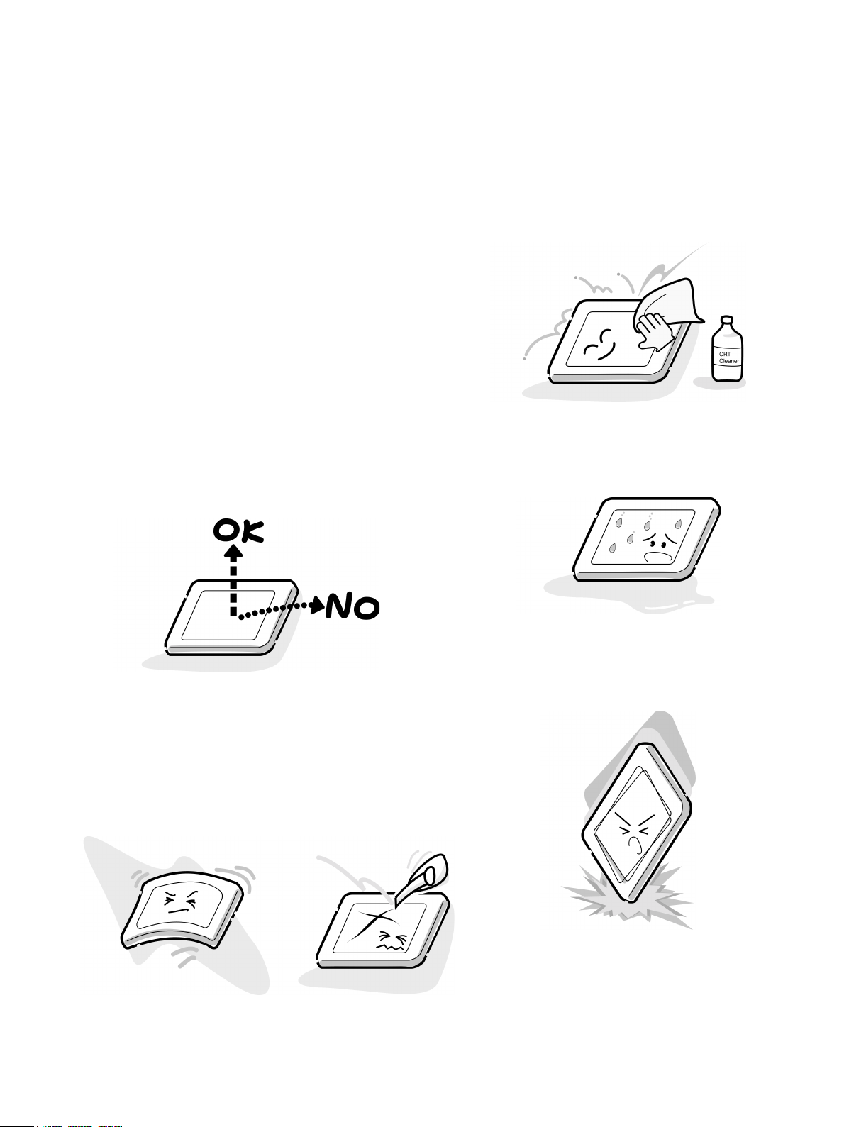
1. When installing the LCD module in the LCD cover, be
sure to seat it so that it is properly aligned and
maximum visibility of the display is maintained.
3. If the panel’s surface gets dirty, wipe it with cotton or
a soft cloth. If it is still dirty, try breathing on the
surface to create a light condensate and wipe it again.
If the surface is very dirty, we recommend a CRT
cleaning agent. Apply the agent to a cloth and then
wipe the panel’s surface. Do not apply cleanser
directly to the panel. Also, never scratch the surface.
4. If water or other liquid is left on the panel’s surface for
a long period, it can change the screen’s tint or stain it.
Be sure to quickly wipe off any liquid.
2. Be careful to align the four holes at the right side and
left side of the LCD module with the corresponding
holes in the LCD cover before securing the module
with four screws. Do not force the module into place,
because stress can affect its performance. Also, the
panel’s polarized surface is easily scarred, so be
careful when handling it.
5. Glass is used in the panel, so be careful not to drop it
or let it strike a hard object, which could cause
breakage or cracks.
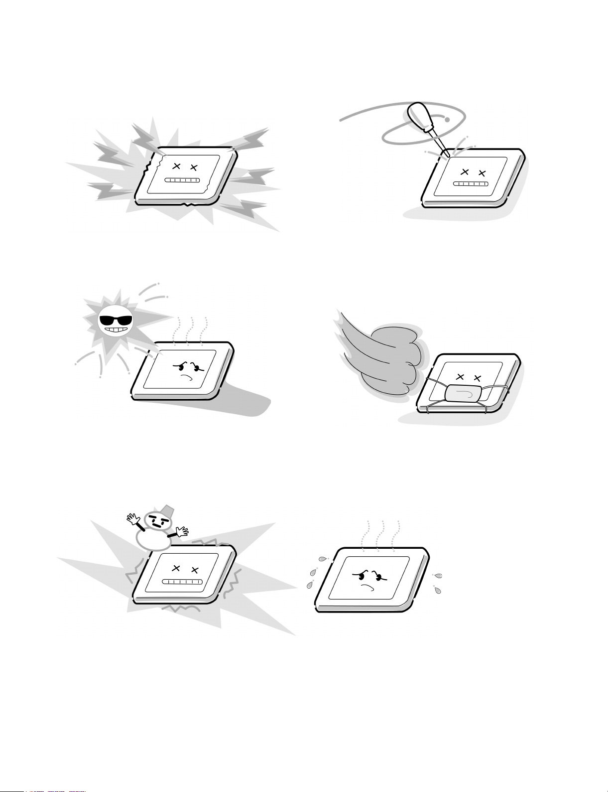
6. CMOS-LSI circuits are used in the module, so guard
against damage from electrostatic discharge. Be sure
to wear a wrist or ankle ground when handling the
module.
9. Do not disassemble the LCD module. Disassembly can
cause malfunctions.
7. Do not expose the module to direct sunlight or strong
ultraviolet rays for long periods.
8. Do not store the module at temperatures below
specifications. Cold can cause the liquid crystals to
freeze, lose their elasticity or otherwise suffer damage.
10. If you transport the module, do not use packing
material that contains epoxy resin (amine) or silicon
glue (alcohol or oxime). These materials can release
gas that can damage the panel’s polarization.

CONTENTS
GENERAL DESCRIPTIONS AND PART REPLACEMENT
1. LOCATION OF PARTS ............................................................. 1-1
1-1. Buttons on the Front Panel, and
Terminals on the Side and the Back Panel ........................ 1-1
1-2. Remote Control ................................................................... 1-2
1-3. Location of Main Parts ....................................................... 1-3
2. REMOVAL .................................................................................. 1-4
2-1. Front Panel .......................................................................... 1-4
2-2. LCD Panel ............................................................................ 1-4
2-3. Inverter PC Board ............................................................... 1-5
2-4. Sensor PC Board ................................................................. 1-6
2-5. LCD Rear Cover ................................................................. 1-6
2-6. Wall Hanging Plate ............................................................. 1-7
2-7. Bottom Cover ....................................................................... 1-7
2-8. Side Cover ............................................................................ 1-7
2-9. Rear Terminal Panel, Main PC Board .............................. 1-7
2-10.Front Net, Speaker .............................................................. 1-8
SERVICING DIAGRAMS
1. CIRCUIT SYMBOLS AND
SUPPLEMENTARY EXPLANATION ..................................... 2-1
1-1. Solid Resistor Indication ..................................................... 2-1
1-2. Inductor Indication ............................................................. 2-1
1-3. Capacitance Indication ....................................................... 2-1
1-4. Waveform and Voltage Measurement .............................. 2-1
1-5. Precautions for Part Replacement ..................................... 2-1
2. BLOCK DIAGRAMS .................................................................. 2-2
2-1. Power Block Diagram ......................................................... 2-2
2-2. Inverter Block Diagram ...................................................... 2-3
2-2-1.
Pin Assignments (microprocessor) IC701: KS88C6348 ...
2-3. Main Block Diagram ........................................................... 2-5
3. CIRCUIT DIAGRAMS ............................................................... 2-7
3-1. Power Supply Circuit Diagram .......................................... 2-7
3-2. Microprocessor Circuit Diagram ....................................... 2-9
2-4
SECTION 1
2-11.Switch PC Board ................................................................. 1-8
2-12.Hinge, Top Cover ................................................................ 1-8
3. GND LEAD WIRE CONNECTION DIAGRAM .................... 1-9
4. TROUBLESHOOTING ............................................................ 1-10
4-1. No Power (No Video & No Sound) .................................. 1-10
4-2. No Video ............................................................................. 1-11
4-2-1. No Video (Sound O.K) .................................................. 1-11
4-2-2. No Video (Sound O.K) .................................................. 1-11
4-3. No Sound (Video O.K) ...................................................... 1-12
SECTION 2
3-3. Input Jack Circuit Diagram ............................................. 2-11
3-4. VPC3230 Circuit Diagram ............................................... 2-13
3-5. TTX&Caption Circuit Diagram ...................................... 2-15
3-6. MXIC Circuit Diagram .................................................... 2-17
3-7. Frame Buffer Circuit Diagram ........................................ 2-19
3-8. Panel Interface Circuit Diagram ..................................... 2-21
3-9. Sound Circuit Diagram ..................................................... 2-23
3-10.Wow Control Circuit Diagram ........................................ 2-25
3-11.Sound Amplifier Circuit Diagram ................................... 2-27
3-12.Pin Voltage ......................................................................... 2-29
3-13.Waveforms ......................................................................... 2-36
4. PC BOARDS .............................................................................. 2-41
4-1. Main PC Board .................................................................. 2-41
4-2. Switch PC Board ............................................................... 2-45
4-3. Sensor PC Board ............................................................... 2-45
SAFETY PRECAUTION ................................................................. 3-1
NOTICE ............................................................................................. 3-1
SECTION 3
PARTS LIST
1. EXPLODED VIEWS ................................................................... 3-2
1-1. Packing Assembly ................................................................ 3-2
1-2. Chassis Assembly ................................................................ 3-3
2. PARTS LIST ................................................................................ 3-4
SECTION 1
GENERAL DESCRIPTIONS AND
PART REPLACEMENT
1. LOCATION OF PARTS
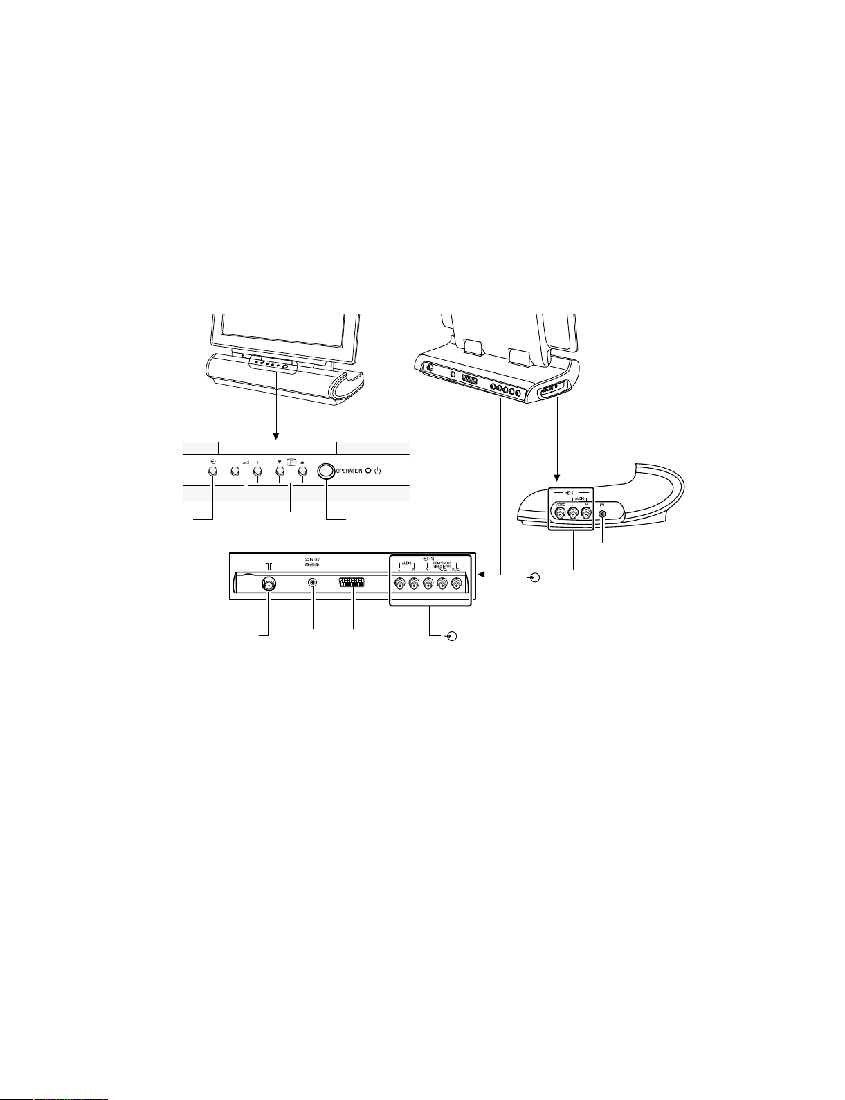
1-1. Buttons on the Front Panel, and Terminals on the Side and the Back Panel
<Front>
TV/Video Power
Volume
up/down
Aerial input DC Input 21Pin
Channel
up/down
SCART input
<Rear>
2
(2) : Video 2 input terminals
(Video Audio L/R)
(1) : Video1 input terminals
(Audio L/R,
Component video input Y, P
Headphone jack
B/CB
, PR/CR)
Fig. 1-1-1
1-1
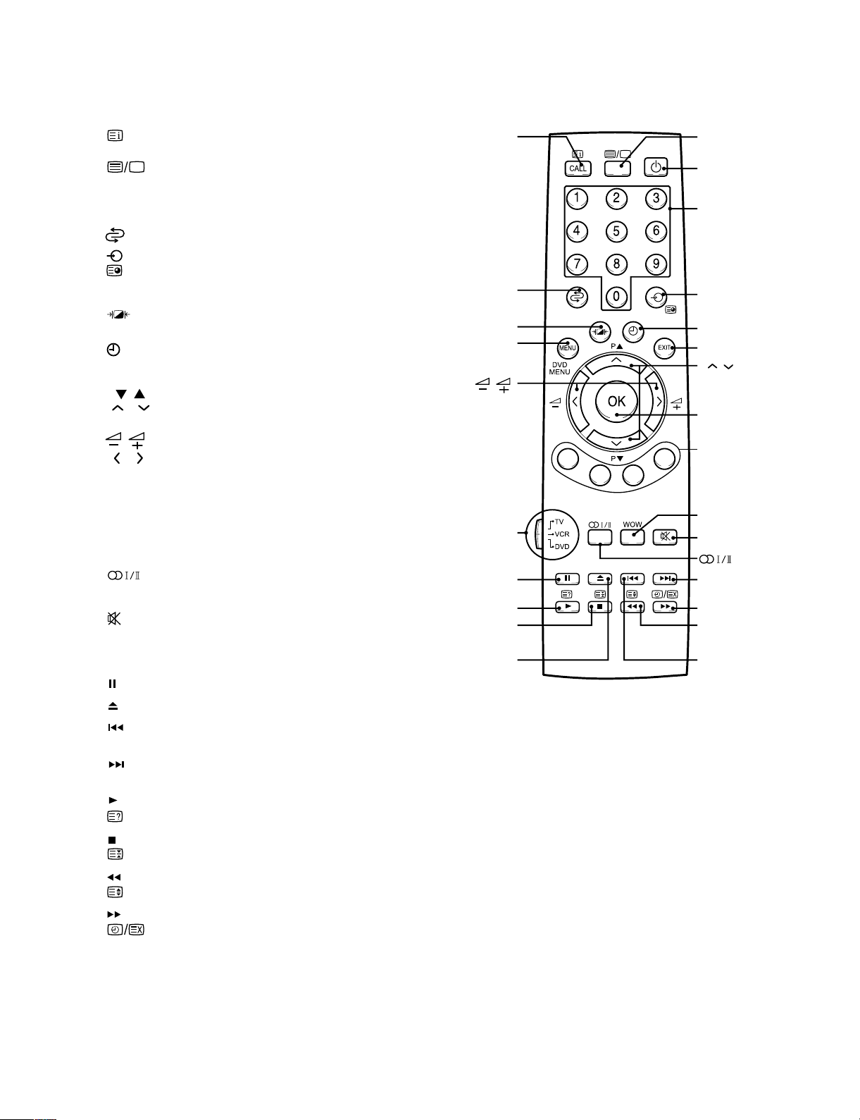
1-2. Remote Control
CALL displays screen information. (TV)
displays teletext initial/index. (TTX)
selects teletext/TV mode.
POWER turns the TV on and off.
CHANNEL NUMBERS allow direct access to channels.
returns to the last viewed channel.
selects the signal input source.
press to display a secondary page. (TTX)
MENU allows access to programming menus. (TV/DVD)
adjusts the TV picture by selecting one of the preset
factory settings.
sets the TV to turn off at a specific time.
EXIT sets menu information and closes menus.
P / cycles through programmed channels.
( / ) Also used to highlight selections on the
on-screen menus.
adjusts the volume level. Also used to increase or
( / ) reduce the value of a menu option.
OK sets programmed menu information.
FAST TEXT TOPIC SELECTION directly access teletext
linked page.
TV/VCR/DVD switch switches among TV,VCR and
DVD inputs.
switches sound mode.
WOW ON/OFF switches sound effect on and off.
mutes the sound.
Note:
Toshiba VCR,DVD can be operated with these buttons.
press to pause or still. (DVD/VCR)
press to open/close the tray. (DVD/VCR)
Prev press to skip back the current chapter or track.
(DVD/VCR)
press to skip forward to the next chapter or track.
(DVD/VCR)
press to play a videotape or disc. (DVD/VCR)
selects hidden content during teletext display. (TTX)
press to stop a videotape or disc. (DVD/VCR)
holds function during teletext display. (TTX)
press to rewind a videotape or disc. (DVD/VCR)
press to change double-size letters. (TTX)
press to fast forward a videotape or disc. (DVD/VCR)
press to cancel the TTX mode or display the accurate time. (TTX)
CALL
Ch RVT
P.STD
MENU
TV/VCR/DVD
PAUSE
PLAY
STOP
OPEN/CLOSE
TEXT/TV
POWER
CHANNEL
NUMBER
TV/VIDEO
TIME
EXIT
P/
OK
FASTTEXT
TOPIC
SELECTION
WOW
MUTE
CHAPTER
NEXT
FAST NEXT
FAST BACK
CHAPTER
BACK
Fig. 1-1-2
1-2
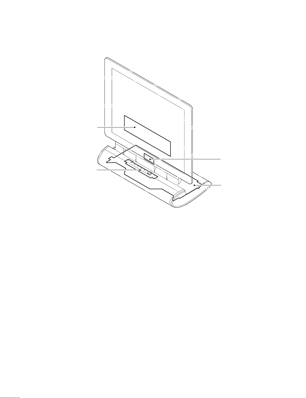
1-3. Location of Main Parts
U004 Inverter PC board
U002 Switch PC board
U003 Sensor PC board
Fig. 1-1-3
U001 Main PC board
1-3
2. REMOVAL
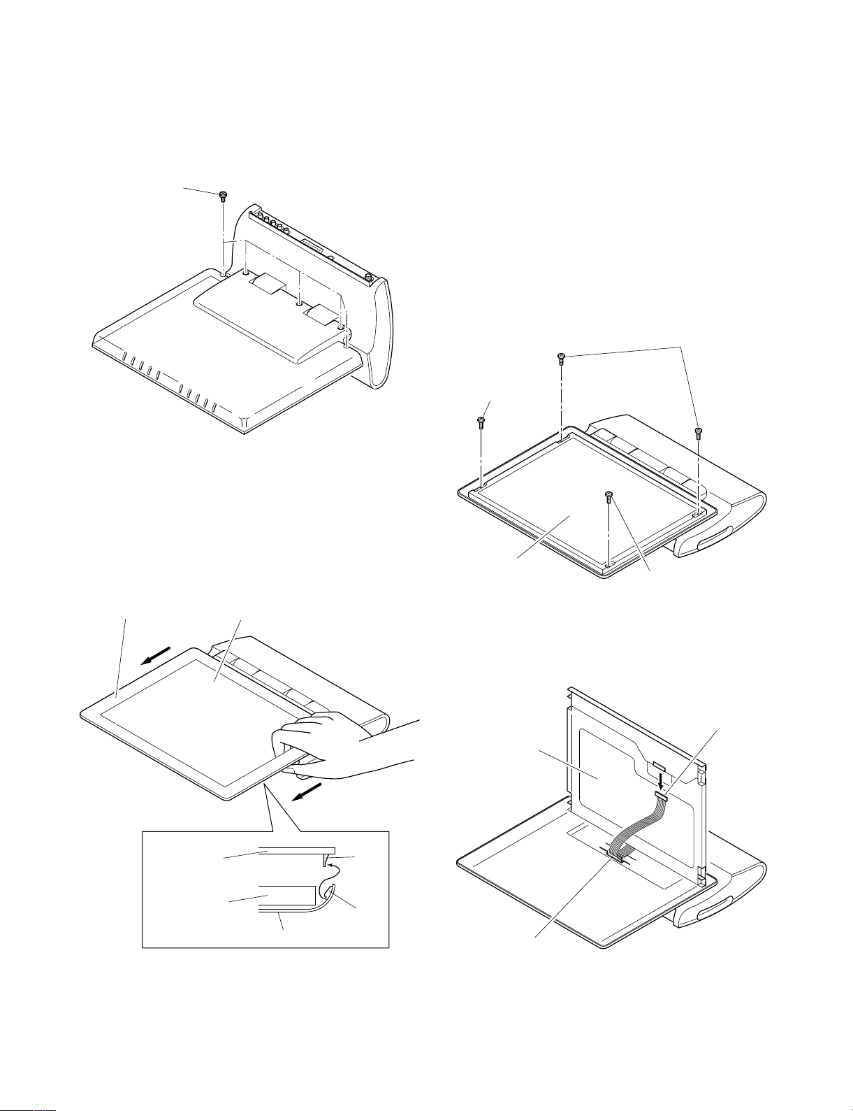
2-1. Front Panel
1. Remove five screws (1).
Screws (1)
Fig. 1-2-1
Note:
• A "snapping" sound will be heard when the claw is
released.
• Take care not to scratch the LCD.
• Caution should be taken to avoid injury from edges on
metal areas when removing the LCD panel.
• Return the wiring to their original positions during
assembly and take care not to get wires caught in the
front panel.
2-2. LCD Panel
1. Remove four screws (1).
Screws (1)
Screw (1)
2. Place the main unit horizontally (similar to use when
hanging on wall), insert finger from the inner side (2)
and release the front panel (2) claws in order from the
bottom (arrow A) (there are eleven peripheral claws).
Front panel (2)
A
Front panel (2)
LCD
LCD
A
Claw
Claw
LCD panel (2)
Screw (1)
Fig. 1-2-3
2. Lift the LCD panel (2) up and remove the connector
(3) from back.
Rear side of
the LCD panel (2)
Connector (3)
Fig. 1-2-2
LCD rear panel
Be careful not to damage
the inverter PC board holder.
Fig. 1-2-4
1-4
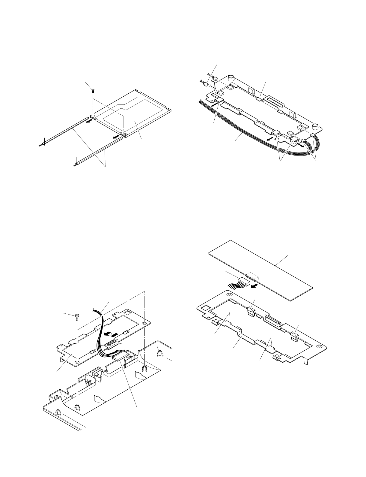
3. Turn the LCD (2) on its back and remove two screws
(4).
4. Slide the back lights (5) on the top and bottom out to
the left side and remove the LCD (2).
Screws (4)
3. Remove the connectors (4) from the four locations and
remove the wire from the three locations of claw B.
Connector (4)
Inverter PC board
holder (2)
Claw B
Rear side of the
LCD panel (2)
Back light (5)
Fig. 1-2-5
Note:
• Return the wiring to their original position when
assembling.
2-3. Inverter PC Board
1. Remove the wire of connector (1) from the inverter PC
board holder (2) claw A.
2. Remove two screws (3).
Wire
Screws (3)
Wire
Claw B
Connector (4)
Fig. 1-2-7
4. Release four claws C, then remove the inverter PC
board holder (2) from the inverter PC board (5).
5. Remove the connector (6) from the one location, then
remove the inverter PC board (5).
Inverter PC board (5)
Connector (6)
Claw C
Claw C
Inverter PC board
holder (2)
Fig. 1-2-6
Claw A
Connector (1)
Claw C
Inverter PC board
holder (2)
Claw C
Fig. 1-2-8
Note:
• Return the wiring to their original position when
assembling.
• The inverter PC board contains high voltage circuitry
and therefore the power supply plug should always be
unplugged during disassembly and assembly.
Additionally, care should be taken when servicing
1-5
while the power is on.
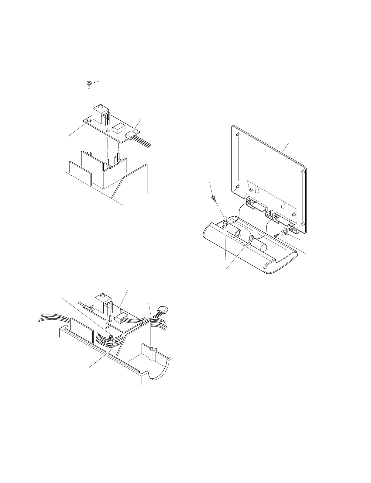
2-4. Sensor PC Board
1. Remove one screw (1) and remove the connector (2)
from the one location, then remove the sensor PC
board (3).
Screw (1)
Connector (2)
2-5. LCD Rear Cover
1. Remove the front panel, the LCD panel and the
inverter PC board. (Refer to item 1-1, 1-2 and 1-3.)
2. Remove two screws (1), then remove the support (2).
3. Remove two screws (3) and remove the LCD rear
cover (4) in a vertical position.
Note:
• If not removed when in a vertical position, the hinges
may become deformed.
Sensor
PC board (3)
Fig. 1-2-9
Note:
• When attaching the sensor PC board (3), bundle the
wires with the band (4) and insert into groove then
attach the sensor PC board (3) from the top.
Sensor PC board (3)
Band (4)
Wires
LCD rear cover (4)
Screws (3)
Support (2)
Screws (1)
Guide
Fig. 1-2-11
Place the bundled wires (4)
into this groove and attach the
sensor PC board (3) on the top.
Fig. 1-2-10
1-6
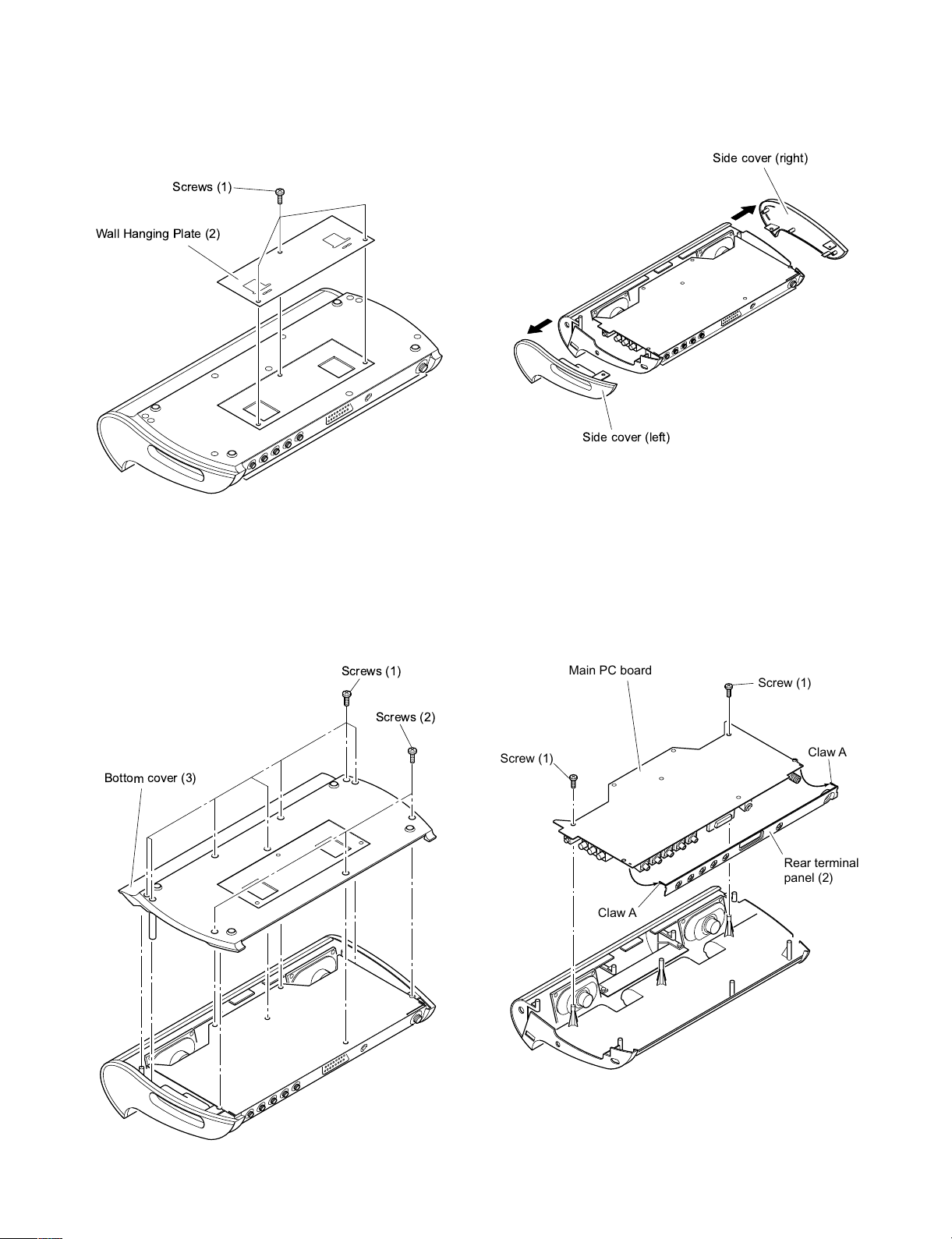
2-6. Wall Hanging Plate
Screw (1)
Screw (1)
Rear terminal
panel (2)
Claw A
Claw A
Main PC board
1. Remove three screws (1), then remove the wall
hanging plate (2).
Screws (1)
Wall Hanging Plate (2)
2-8. Side Cover
1. Remove the left and right side covers.
Side cover (right)
Side cover (left)
Fig. 1-2-14
Fig. 1-2-12
2-7. Bottom Cover
1. Remove seven screws (1) and three screws (2), then
remove the bottom cover (3).
Screws (1)
Screws (2)
Bottom cover (3)
2-9. Rear Terminal Panel, Main PC
Board
1. Remove two screws (1).
2. Remove two claws A, then remove the rear terminal
panel (2).
Fig. 1-2-15
Fig. 1-2-13
1-7
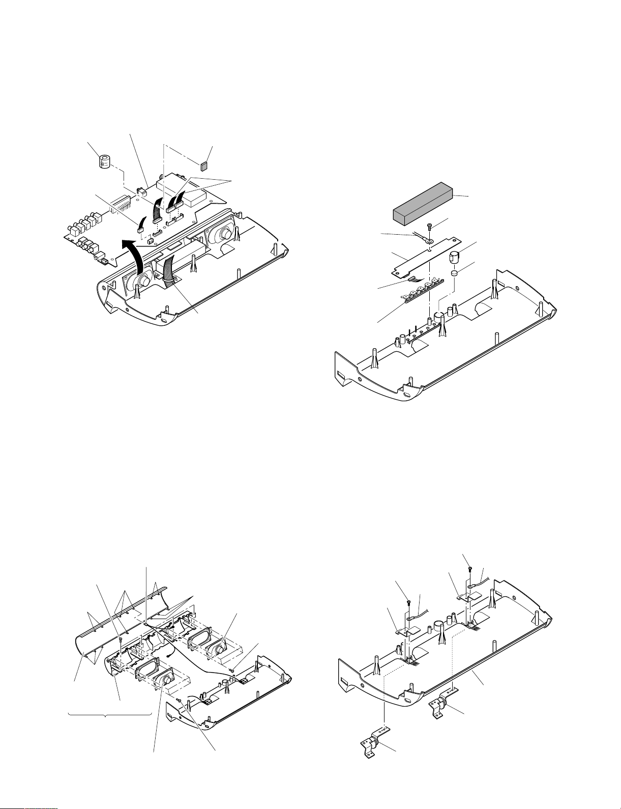
3. Remove the core (5) and the cushion (6) from the 20
Cushion (1)
Connector (2)
Screw (3)
Switch PC board (4)
GND lead wire
Power button cover (5)
Power button (6)
5-knob switch
button (7)
pin connector (4).
4. Remove the connectors (4) from the four locations,
then remove the main PC board (7).
Core (5)
Main PC board (7)
Cushion (6)
2-11.Switch PC Board
1. Remove the cushion (1).
2. Remove the connector (2).
3. Remove one screw (3), then remove the switch PC
board (4).
4. Remove the power button cover (5), the power button
(6) and the 5-knob switch button (7).
Connector (4)
Note:
• Return the wiring to their original positions during
2-10.Front Net, Speaker
1. Remove four screws (1).
2. Remove the GND lead wire (2), then remove the front
3. Remove four screws (4), then remove the right speaker
4. The front net assembly (3) will come apart to the front
Claw A
Front net (8)
Connectors (4)
Bundled wires
Fig. 1-2-16
assembly.
net assembly (3).
(5), four screws (6) and the left speaker (7).
net (8) and the chassis (9) when claws A are released.
GND lead wire (2)
Screws (1)
Claw A
Front net assembly (3)
Claw A
Chassis (9)
Claw A
Left speaker (7)
Claw A
Right speaker (5)
Screws (4)
Screws (6)
Fig. 1-2-18
2-12.Hinge, Top Cover
1. Remove two screws (1), remove the left support (2)
and the left hinge (3).
2. Remove two screws (4), the right support (5) and the
right hinge (6), then remove the top cover (7).
Screws (4)
GND lead wire
Top cover (7)
Right hinge (6)
Screws (1)
Left support (2)
Right
support (5)
GND
lead wire
Left hinge (3)
Fig. 1-2-17
1-8
Fig. 1-2-19
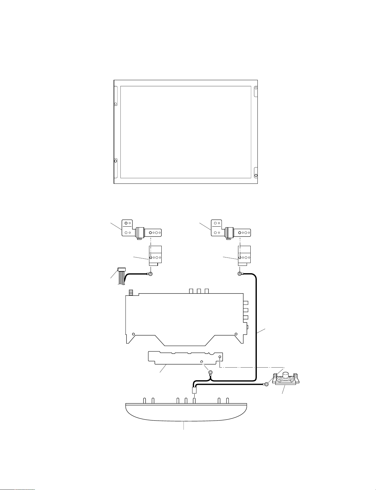
3. GND LEAD WIRE CONNECTION DIAGRAM
When assembling, refer to the diagram below for the GND lead wire connection.
LCD
Left
hinge
Connector
Left
support
Right
hinge
Right
support
Main PC board
GND lead wire
Switch PC board
Front net
Fig. 1-3-1
1-9
Right speaker
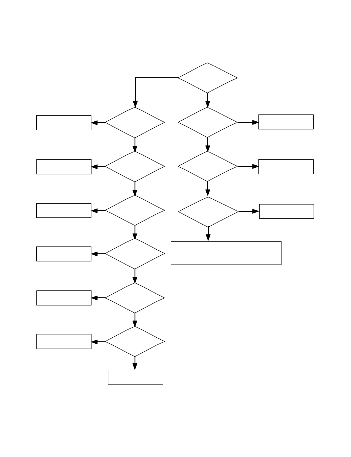
4. TROUBLESHOOTING
4-1. No Power (No Video & No Sound)
12Vcc = 12V ?
(IC801 Pin 5)
CHECK/REPLACE
F801, L801, ADAPTER
CHECK/REPLACE
IC801
CHECK/REPLACE
Q801
CHECK/REPLACE
IC702
N
N
IC801
Pin 1 = 12V ?
5Vcc = 5V ?
Y
Y
IC801
Pin 4 = LOW ?
3.3Vcc = 3.3V ?
N
Y
IC701
Pin 19 = HIGH ?
IC201 Pin 34, 35
N
N
IC701
Pin 11 = 5V ?
IC201 (MXCS, MXSDA, MXSCL, MX_RESET),
Y
Y
Y
OSC O.K ?
Y
CHECK/REPLACE
IC400
N
N
N
CHECK/REPLACE
IC803, L804, D802
CHECK/REPLACE
IC804
CHECK/REPLACE
X201, IC201
CHECK/REPLACE
IC704
CHECK/REPLACE
X701, IC701
N
Pin 18 = HIGH ?
N
IC701 Pin 13, 14
OSC O.K ?
CHECK/REPLACE
SCL, SDA LINE
Y
IC701
Y
Y
Fig. 1-4-1
1-10
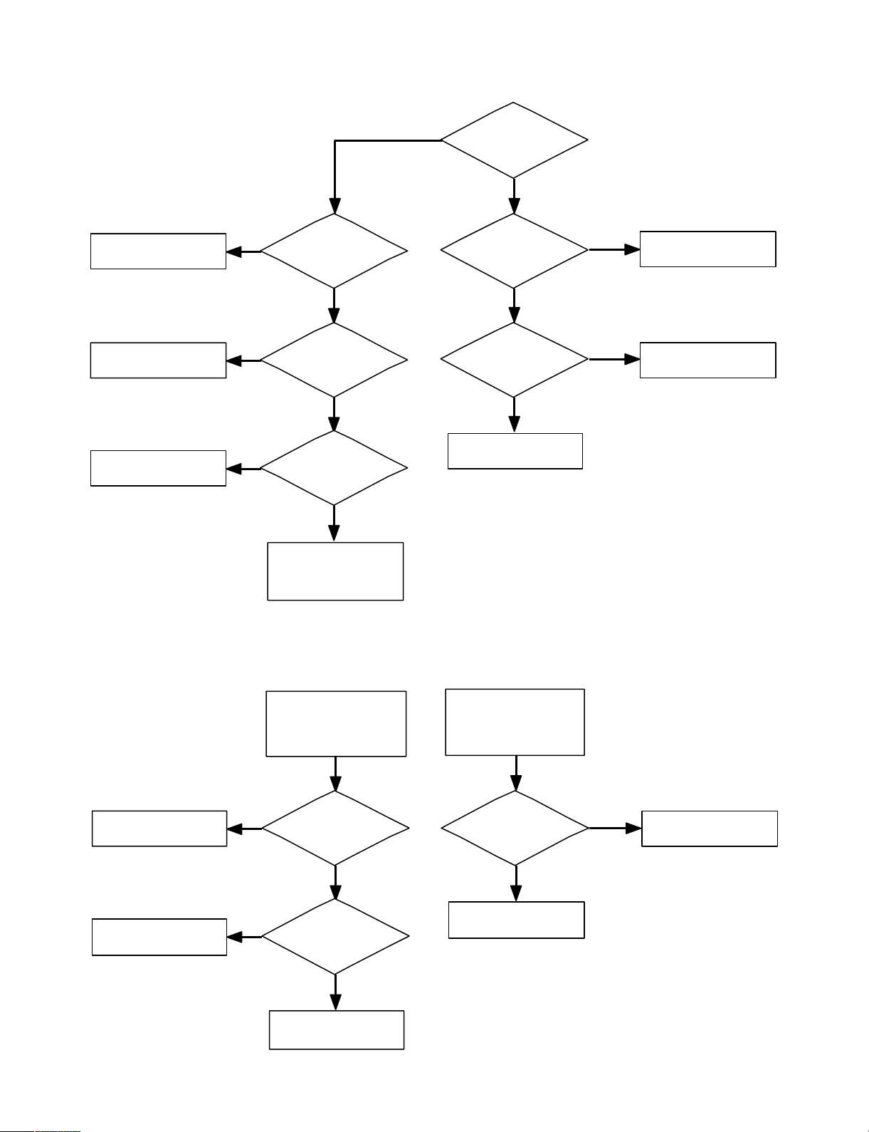
4-2. No Video
4-2-1. No Video (Sound O.K)
OSD DISPLAY
O.K ?
CHECK/REPLACE
IC701, INVERTER
CHECK/REPLACE
IC201, IC301
CHECK/REPLACE
IC302, Q301, IC701
N
LCD PANEL
LAMP ON ?
N
OUTPUT O.K ?
N
Pin = 3.3V ?
CHECK/REPALCE
LCD PANEL,
INTERFACE CABLE
Y
IC301
Y
IC301
Y
N
IC201 PDA [0..23]
SIGNAL O.K ?
Y
Y
CHECK/REPLACE
IC201
N
IC101
Pin 62, 63 OSC O.K ?
N
CHECK/REPLACE
X101, IC101
Y
CHECK/REPLACE
IC101
4-2-2. No Video (Sound O.K)
CHECK/REPLACE
IC101, D104, L105
CHECK/REPLACE
IC501, IC601
Y
Y
RF MODE O.K
A/V MODE NG ?
IC501 Pin 7
SIGNAL O.K ?
N
IC501 Pin 1, 3
INPUT SIGNAL O.K ?
N
CHECK
INPUT CABLE
Fig. 1-4-2
RF MODE N.G
A/V MODE O.K ?
IC502 Pin 3
SIGNAL O.K ?
N
CHECK/REPLACE
TU1, Q502
Y
CHECK/REPLACE
IC502, Q501, IC601
Fig. 1-4-3
1-11
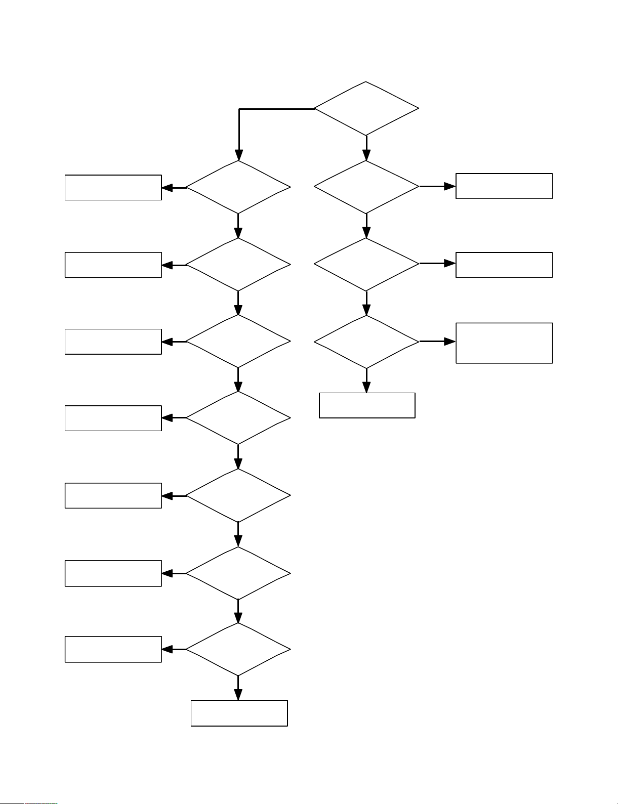
4-3. No Sound (Video O.K)
IC601 Pin 27, 28
OUTPUT O.K ?
CHECK/REPLACE
IC601, L601, L602
CHECK/REPLACE
IC802
CHECK/REPLACE
IC601, X601
CHECK/REPLACE
IC701, IC601
N
IC601 Pin 66, 65
11, 12, 13 = 5V ?
Y
N
IC601
Pin 39 = 8V ?
Y
N
IC601
Pin 71, 72 OSC O.K ?
Y
N
IC601 Pin 21
(A_RESET) = HIGH ?
N
IC681 Pin 4, 6
OUTPUT O.K ?
Y
Y
CHECK/REPLACE
SPEAKER, WIRE
N
IC681
Pin 7 = 12V ?
N
CHECK/REPLACE
IC681, R681
Y
IC681
Pin 8 = HIGH ?
N
CHECK/REPLACE
IC681, Q681
Q682, Q683
Y
CHECK/REPLACE
IC681
CHECK/REPLACE
IC601
CHECK/REPLACE
IC651
CHECK/REPLACE
IC601
Y
Y
IC601 Pin 47, 48
INPUT O.K ?
N
Y
IC601 Pin 33, 34
OUTPUT O.K ?
N
Y
IC601
INPUT O.K ?
N
CHECK
AUDIO INPUT JACK
Fig. 1-4-4
1-12
 Loading...