

(
XCM519 Series
600mA Synchronous Step-Down DC/DC Converter + Low Voltage Input LDO
■GENERAL DESCRIPTION
The XCM519 series is a multi combination module IC which comprises of a 600mA driver transistor built-in synchronous
step–down DC/DC converter and a low voltage input LDO regulator. The device is housed in small USP-12B01 package which
is ideally suited for space conscious applications. Battery operated portable products require high efficiency so that a dual
DC/DC converter is often used. The XCM519 can replace this dual DC/DC to eliminate one inductor and reduce output noise.
The DC/DC converter and the LDO regulator blocks are isolated in the package so that noise interference from the DC/DC to
the LDO regulator is minimal.
A low output voltage and low On-resistance LDO regulator is added in series to the DC/DC output so that one another low output
voltage is created with a high efficiency and low noise. With comparison to the dual DC/DC solution, one inductor can be
eliminated which results in parts reduction and board space saving.
■APPLICATIONS
●Mobile phones, Smart phones
Bluetooth equipment
●
Portable communication modems
●
●Portable game consoles
■ TYPICAL APPLICATION CIRCUIT
* The dashed lines denote the connection using
through-holes at the backside of the PC board.
■TYPICAL PERFORMANCE
CHARACTERISTICS
Dropout Voltage vs. Output Current
300
250
200
150
100
50
Dropout Voltage: Vdif(mV)
0
0 100 200 300 400
TOP VIEW)
VROUT=1.2V
Ta=25℃
VBIAS=3.0V
VBIAS=3.3V
VBIAS=3.6V
VBIAS=4.2V
VBIAS=5.0V
Output Current: IOUT(mA)
■FEATURES
<DC/DC Converter Block>
Input Voltage Range : 2.7V ~ 6.0V
Output Voltage Range : 0.8V ~ 4.0V
High Efficiency : 92% (TYP.)
Output Current : 600mA (MAX.)
Oscillation Frequency : 1.2MHz, 3.0MHz (+15%)
Maximum Duty Cycle : 100%
Soft-Start Circuit Built-In
Current Limiter Circuit
Built-In
Control Methods : PWM (XCM519A)
PWM/PFM Auto (XCM519B)
*Performance depends on external components and wiring on PCB wiring.
<Regulator Block>
Maximum Output Current
Dropout Voltage : 35mV@I
(at V
Bias Voltage Range : 2.5V ~ 6.0V
Input Voltage Range : 1.0V ~ 3.0V (V
Output Voltage Range : 0.7V ~ 1.8V (0.05V increments)
High Output Accuracy : ±20mV
Supply Current : I
Stand-by Current : I
UVLO : V
Thermal Shut Down :
Soft-start Time : 240μs@V
CL High Speed Auto-Discharge
Low ESR Capacitor : Ceramic Capacitor Compatible
Operating Ambient Temperature
Package
Environmentally Friendly
Standard Voltage Combinations : DC/DC VR
XCM519xx01Dx 1.8V 1.2V
XCM519xx02Dx 1.8V 1.5V
XCM519xx03Dx 1.5V 1.2V
XCM519xx04Dx 1.8V 1.0V
XCM519xx05Dx 1.5V 1.0V
*Other combinations are available as semi-custom products.
(Constant Current & Latching)
: 400mA (Limiter 550mA TYP.)
=100mA (TYP.)
OUT
-
V
BIAS
ROUT(E)
(V
BIAS
IN2≦VBIAS
=25μA , I
BIAS
=0.01μA , I
BIAS
=2.0V , V
BIAS
IN2
Detect 150℃, Release 125℃ (TYP.)
=1.2V(TYP.)
ROUT
: -40℃ ~ +85℃
: USP-12B01
:
EU RoHS Compliant, Pb Free
ETR2421-005
=2.4V)
- V
ROUT(E)
=0.9V)
)
=1.0μA (TYP.)
IN2
=0.01μA (TYP.)
IN2
=0.4V (TYP)
1/49
XCM519 Series
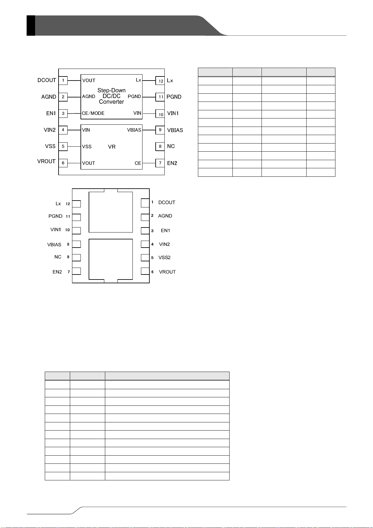
■PIN CONFIGURATIOIN
DC/DC
(*1)
V
SS
VR
(*2)
V
BIAS
NOTE:
* The DC/DC ground pin (No. 2 and 11) should be connected for use.
* Two dissipation pads on the reverse side of the package should be electrically isolated.
(*1): Electrical potential of the dissipation pad should be V
(*2): Electrical potential of the dissipation pad should be V
Care must be taken for an electrical potential of each dissipation pad so as to enhance mounting strength and heat release
when the pad needs to be connected to the circuit.
(BOTTOM VIEW)
■PIN ASSIGNMENT
PIN No XCM519 FUNCTIONS
1 DCOUT
DC/DC Block: Output Voltage
2 AGND DC/DC Block: Analog Ground
3 EN1 DC/DC Block: Chip Enable
4 V
5 V
Voltage Regulator Block: Power Input
IN2
Voltage Regulator Block: Ground
SS2
6 VROUT Voltage Regulator Block: Output
7 EN2 Voltage Regulator Block: Enable
8 NC No Connection
9 V
10 V
Voltage Regulator Block: Power Input
BIAS
DC/DC Block: Power Input
IN1
11 PGND DC/DC Block: Power Ground
12 Lx DC/DC Block: Switching
2/49
PIN No.
1 DCOUT V
XCM519 DC/DC VR
OUT
2 AGND AGND ―
3 EN1 CE ―
4 V
5 V
― V
IN2
― V
SS2
6 VROUT ― V
7 EN2 ― CE
8 NC ― ―
9 V
10 V
― V
BIAS
V
IN1
―
IN
11 PGND PGND ―
12 Lx Lx ―
level.
SS
level.
BIAS
―
OUT
BIAS
IN
SS

X
■PRODUCT CLASSIFICATION
●Ordering Information
XCM519A①②③④⑤-⑥
XCM519B①②③④⑤
DESIGNATOR ITEM SYMBOL DESCRIPTION
①
② ③
(*1)
④⑤-⑥
(*1)
The “-G” suffix indicates that the products are Halogen and Antimony free as well as being fully RoHS compliant.
Package (Order Unit) DR-G USP-12B01 (3,000/Reel)
(*1)
DC/DC BLOCK:PWM fixed control
(*1)
-⑥
DC/DC BLOCK:PWM/PFM automatic switching control
Oscillation Frequency and Options - See the chart below
Output Voltage
-
Internally set sequential number relating to output voltage
(See the chart below)
●DESIGNATOR①
DC/DC BLOCK Voltage Regulator BLOCK
①
A 1.2M Not Available Standard Not Available
B 3.0M Not Available Standard Not Available
C 1.2M Available High Speed Not Available
D 3.0M Available High Speed Not Available
OSCILLATION
FREQUENCY
CL AUTO
DISCHARGE
SOFT START Pull-down
●DESIGNATOR②③
②③
01 1.8V 1.2V
02 1.8V 1.5V
03 1.5V 1.2V
04 1.8V 1.0V
05 1.5V 1.0V
*When the DCOUT pin is connected to V
*This series are semi-custom products. For other combinations of output voltages please consult with your Torex sales contact.
DCOUT VROUT
, DCOUT pin output voltage can be fixed in the range of 1.0V~3.0V.
IN2
CM519
Series
3/49
XCM519 Series
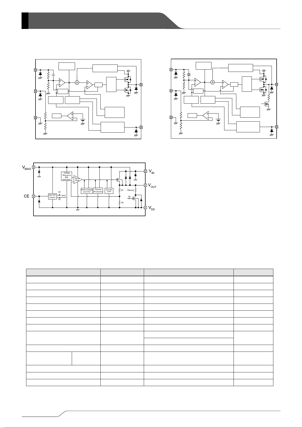
■BLOCK DIAGRAMS
Step-Down DC/DC Converter
XC9235A/XC9236A
R3
R4
Error Amp.
Vref with
Soft Start,
CE
UVLO
Phase
Compensation
VSHORT
PWM/PFM
Selector
UVLO Cmp
PWM
Comparator
Current Feedback
Current Limit
Logic
Synch
Buffer
Drive
Ramp Wave
Generator
OSC
CE/MODE
Control
Logic
Lx
CE
V
OUT
V
IN
V
SS
V
OUT
R2
V
R1
IN
V
SS
VR
* XCM519 series A type is a fixed PWM because that the “CE/MODE Control Logic” outputs a low level signal to the “PWM/PFM Selector”.
* XCM519 series B type is an auto PWM/PFM switching because the “CE/MODE Control Logic” outputs a high level signal to the “PWM/PFM Selector”.
*Diodes inside the circuit are an ESD protection diode and a parasitic diode.
■MAXIMUM ABSOLUTE RATINGS
Ta =2 5 ℃
PARAMETER SYMBOL RATINGS UNITS
V
Voltage V
IN1
- 0.3 ~ 6.5 V
IN1
Lx Voltage VLx - 0.3 ~ V
DCOUT Voltage V
EN1 Voltage V
- 0.3 ~ 6.5 V
DCOUT
- 0.3 ~ 6.5 V
EN1
Lx Current ILx ±1500 mA
V
Voltage V
BIAS
V
Voltage
IN2
VROUT Current
VROUT Voltage V
EN2 Voltage V
Power Dissipation
(Ta=25℃)
USP-12B01 Pd 150 mW
V
BIAS
V
V
IN2
700
I
VROUT
ROUT
V
EN2
Junction Temperature Tj 125 ℃
Operating Ambient Temperature Topr -40~+85 ℃
Storage Temperature Tstg -55~+125 ℃
(*1)
I
=Less than Pd / (V
VROUT
IN2-VROUT
)
4/49
Step-Down DC/DC Converter
XC9235B/XC9236B
Available with CL Discharge, High Speed Soft-Start
Available with CL Discharge, High Speed Soft-Start
Phase
Compensation
R2
Error Amp.
R1
SS
SS
VSS - 0.3~V
- 0.3~V
V
SS
SS
VSHORT
Vref with
Soft Start,
CE
UVLO
R3
R4
+ 0.3 or 6.5 V
IN1
- 0.3 ~ 7.0 V
- 0.3 ~ 7.0 V
(*1)
mA
+ 0.3
BIAS
+ 0.3
IN2
- 0.3 ~ 6.5 V
、)(CL放電機能有 高速ソフトスタート
Current Feedback
Current Limit
PWM
Comparator
Logic
PWM/PFM
Selector
UVLO Cmp
Synch
Buffer
Drive
Ramp Wave
Generator
OSC
CE/MODE
Control
Logic
Lx
CE/
CE
V

X
■ELECTRICAL CHARACTERISTICS
CM519
Series
●XCM519xA (DC/DC BLOCK) V
DCOUT
=1.8V, f
=1.2MHz, Ta=25℃
OSC
PARAMETER SYMBOL CONDITIONS MIN. TYP. MAX. UNITS
Output Voltage V
Operating Voltage Range V
Maximum Output Current I
UVLO Voltage V
Supply Current IDD
Stand-by Current I
Oscillation Frequency f
PFM Switching Current I
PFM Duty Limit D
Maximum Duty Ratio D
Minimum Duty Ratio D
Efficiency
(*2)
EFFI
Lx SW "H" ON Resistance 1 R
Lx SW "H" ON Resistance 2 R
Lx SW "L" ON Resistance 1 R
Lx SW "L" ON Resistance 2 R
Lx SW "H" Leak Current
Lx SW "L" Leak Current
Current Limit
Output Voltage
Temperature
Characteristics
(*5)
I
(*5)
I
(*9)
I
△
(V
DCOUT
EN1 "H" Level Voltage V
EN1 "L" Level Voltage V
EN1 "H" Current I
EN1 "L" Current I
Soft Start Time tSS
Latch Time t
Short Protection
Threshold Voltage
DCOUT
IN1
OUT1MAX
UVLO
STB
OSC
PFM
LIMIT_PFM
MAX
MIN
LXH
LXH
LXL
LXL
LEAKH
LEAKL
LIM
V
DCOUT
・△
EN1H
EN1L
EN1H
EN1L
LAT
V
SHORT
When connected to external components,
V
= V
IN1
2.7 - 6.0 V
When connected to external components,
V
IN1=VDCOUT(T)
V
EN1=VIN1, VDCOUT
Voltage which Lx pin holding “L” level
V
IN1=VEN1
V
V
V
V
=5.0V, V
IN1
When connected to external components,
V
IN1=VDCOUT(T)
When connected to external components,
V
IN1=VDCOUT(T)
EN1=VIN1
= V
IN1
= V
IN1
When connected to external components,
V
EN1=VIN1=VDCOUT(T)
V
V
V
V
V
V
V
/
Topr)
V
V
= V
IN1
= V
IN1
= V
IN1
= V
IN1
= V
IN1
= V
IN1
IN1=VEN1
I
=30mA
OUT1
-40℃≦Topr≦85℃
V
DCOUT
Voltage changes Lx to “H” level
V
DCOUT
Voltage changes Lx to “L” level
IN1=VEN1
=5.0V, V
IN1
When connected to external components,
V
=0V → V
EN1
V
= VEN=5.0V, V
IN
Short Lx at 1Ω resistance
Sweeping V
1Ω resistance, V
level within 1ms
Test conditions: Unless otherwise stated, VIN = 5.0V, V
=5.0V, I
EN1
+2.0V, V
OUT1
=30mA
=1.0V
EN1
=0V,
=5.0V,
V
=
V
DCOUT
DCOUT(T)
=(C-1), I
=5.0V, V
EN1
=5.0V, V
EN1
=5.0V, V
EN1
=3.6V, V
EN1
=5.0V
EN1
=3.6V
EN1
DCOUT
DCOUT
=5.0V, V
=0V, V
EN1
+2.0V,V
+2.0V, V
OUT1
(*4)
(*4)
=5.0V, V
=5.0V, V
DCOUT
=
V
DCOUT
=1.0V, I
EN1
=V
EN1
IN1
(*11)
=1mA
=
V
DCOUT
DCOUT(T)
=
V
DCOUT
DCOUT(T)
(*7)
+1.2V
DCOUT
DCOUT
, I
=0V,ILX=100mA
=0V,ILX=100mA
- 0.45 0.66 Ω
- 0.52 0.77 Ω
=0V, VLX=0V - 0.01 1.0 μA
EN1
=0V, VLX=5.0V - 0.01 1.0 μA
EN1
=
V
DCOUT(T)
=0V, Applied voltage to V
=0V, Applied voltage to V
=5.0V, V
EN1
IN1
DCOUT
=0V - 0.1 - 0.1 μA
DCOUT
=0V, V
, I
OUT1
DCOUT
, V
DCOUT
=0V - 0.1 - 0.1 μA
DCOUT
=1mA
=0.8×V
(*6)
= 5.0V, Short Lx at
IN1=VEN1
voltage which Lx becomes “L”
= Setting voltage
DCOUT(T)
(*8)
(*1, *10)
×1.1V
DCOUT(T)
, I
(XCM519AA)
(XCM519BA)
×1.1V - 0 1.0 μA
(*11)
(*11)
OUT1
OUT1
=100mA
=1mA
- 200 - %
×0.9V 100 - - %
×1.1V - - 0 %
=100mA
OUT1
(*3)
- 0.35 0.55 Ω
(*3)
- 0.42 0.67 Ω
×0.9V 900 1050 1350 mA
EN,
(*10)
EN,
(*10)
DCOUT(T)
1.764 1.800 1.836 V ①
600 - - mA
1.00 1.40 1.78 V
- 22 50
- 15 33
1020 1200 1380 kHz
120 160 200 mA
- 92 - %
- ±100 - ppm/ ℃
0.65 - 6.0 V
V
- 0.25 V
SS
0.5 1.0 2.5 ms
1.0 - 20.0 ms
0.675 0.900 1.125 V
μA
NOTE:
*1: Including hysteresis width of operating voltage.
*2: EFFI = { ( output voltage×output current ) / ( input voltage×input current) }×100
*3: ON resistance (Ω)= (V
- Lx pin measurement voltage) / 100mA
IN
*4: Design value
*5: When temperature is high, a current of approximately 10μA (maximum) may leak.
*6: Time until it short-circuits DCOUT with GND via 1Ωof resistor from an operational state and is set to Lx=0V from current limit pulse
generating.
*7: V
+1.2V<2.7V, VIN=2.7V.
DCOUT(T)
*8: When the difference between the input and the output is small, some cycles may be skipped completely before current maximizes.
If current is further pulled from this state, output voltage will decrease because of P-ch driver ON resistance.
*9: Current limit denotes the level of detection at peak of coil current.
*10: "H"=V
*11: XCM519A series exclude I
- 1.2V, "L"=+ 0.1V ~ - 0.1V
IN~VIN
and MAXI
PFM
because those are only for the PFM control’s functions.
PFM
* The electrical characteristics above are when the other channel is in stop mode.
CIRCUIT
①
①
③
②
②
①
①
①
②
②
①
④
④
-
-
⑤
⑤
⑥
①
③
③
⑤
⑤
①
⑦
⑦
5/49
XCM519 Series
■ELECTRICAL CHARACTERISTICS (Continued)
●XCM519xB 1ch (DC/DC BLOCK) V
DCOUT
=1.8V, f
=3.0MHz, Ta=25℃
OSC
PARAMETER SYMBOL CONDITIONS MIN. TYP. MAX. UNITS
Output Voltage V
Operating Voltage Range V
Maximum Output Current I
UVLO Voltage V
DCOUT
2.7 - 6.0 V
IN1
OUT1MAX
UVLO
Supply Current IDD
Stand-by Current I
Oscillation Frequency f
PFM Switching Current I
PFM Duty Limit D
Maximum Duty Ratio D
Minimum Duty Ratio D
V
STB
OSC
PFM
LIMIT_PFM
V
MAX
V
MIN
Efficiency EFFI
Lx SW "H" ON Resistance 1 R
Lx SW "H" ON Resistance 2 R
Lx SW "L" ON Resistance 1 R
Lx SW "L" ON Resistance 2 R
Lx SW "H" Leak Current
Lx SW "L" Leak Current
Current Limit
(*5)
I
(*5)
I
(*9)
I
Output Voltage
Temperature
Characteristics
(V
EN1 "H" Level Voltage V
EN1 "L" Level Voltage V
EN1 "H" Current I
EN1 "L" Current I
V
LXH
V
LXH
V
LXL
V
LXL
V
LEAKH
V
LEAKL
V
LIM
△
V
DCOUT
・△
To p r )
DCOUT
EN1H
EN1L
V
EN1H
V
EN1L
Soft Start Time tSS
Latch Time t
Short Protection
Threshold Voltage
V
LAT
SHORT
Test conditions: Unless otherwise stated, V
When connected to external components,
V
= V
IN1
When connected to external components,
V
IN1=VDCOUT(T)
V
EN1=VIN1, VDCOUT
=5.0V, I
EN1
+2.0V, V
OUT1
=0V,
=30mA
=1.0V
EN1
Voltage which Lx pin holding “L” level
V
=5.0V, V
IN1=VEN1
=5.0V, V
IN1
DCOUT=VDCOUT(T)
=0V, V
EN1
DCOUT=VDCOUT(T)
When connected to external components,
V
IN1=VDCOUT(T)
+2.0V,V
EN1
=1.0V, I
When connected to external components,
V
IN1=VDCOUT(T)
V
EN1=VIN1
IN1=VEN1
IN1=VEN1
+2.0V, V
=(C-1) I
=5.0V, V
=5.0V, V
=V
EN1
(*11)
=1mA
OUT1
DCOUT=VDCOUT(T)
DCOUT=VDCOUT(T)
IN1
When connected to external components,
V
EN1=VIN1=VDCOUT(T)
= V
IN1
= V
IN1
= V
IN1
= V
IN1
= V
IN1
= V
IN1
IN1=VEN1
/
I
=30mA
OUT1
-40℃≦Topr≦85℃
V
DCOUT
=5.0V, V
EN1
=3.6V, V
EN1
=5.0V
EN1
=3.6V
EN1
DCOUT
DCOUT
=5.0V, V
=0V, Applied voltage to V
+1.2V, I
OUT1
=0V,ILX=100mA
DCOUT
=0V,ILX=100mA
DCOUT
(*4)
- 0.45 0.66 Ω
(*4)
- 0.52 0.77 Ω
=5.0V, V
=5.0V, V
=0V, VLX=0V - 0.01 1.0 μA
EN1
=0V, VLX=5.0V - 0.01 1.0 μA
EN1
DCOUT=VDCOUT(T)
Voltage changes Lx to “H” level
V
=0V, Applied voltage to V
DCOUT
Voltage changes Lx to “L” level
IN1=VEN1
=5.0V, V
IN1
=5.0V, V
EN1
=0V - 0.1 - 0.1 μA
DCOUT
=0V, V
=0V - 0.1 - 0.1 μA
DCOUT
When connected to external components,
V
=0V → V
EN1
V
IN1=VEN1
Short Lx at 1Ω resistance
Sweeping V
1Ω resistance, V
“L” level within 1ms
=5.0V, V
IN1
DCOUT(T)
, I
IN1
DCOUT
OUT1
DCOUT
, V
DCOUT
IN1=VEN1
=5.0V, V
= Nominal voltage
=1mA
=0.8×V
(*6)
=5.0V, Short Lx at
voltage which Lx becomes
(*8)
(*1, *10)
×1.1V
(XCM519AB) - 46 65
(XCM519BB) - 21 35
×1.1V - 0 1.0 μA
=100mA
OUT1
=1mA
(*11)
, I
OUT1
- 200 300 %
×0.9V 100 - - %
×1.1V - - 0 %
=100mA
(*3)
- 0.35 0.55 Ω
(*3)
- 0.42 0.67 Ω
×0.9V 900 1050 1350 mA
EN,
(*10)
EN,
(*10)
DCOUT(T)
1.764 1.800 1.836 V ①
600 - - mA
1.00 1.40 1.78 V
2550 3000 3450 kHz
170 220 270 mA
- 86 - %
- ±100 - ppm/ ℃
0.65 - 6.0 V
V
- 0.25 V
SS
0.5 0.9 2.5 ms
1.0 - 20 ms
0.675 0.900 1.125 V
NOTE:
*1: Including hysteresis width of operating voltage.
*2: EFFI = { ( output voltage×output current ) / ( input voltage×input current) }×100
*3: ON resistance (Ω)= (V
- Lx pin measurement voltage) / 100mA
IN
*4: Design value
*5: When temperature is high, a current of approximately 10μA (maximum) may leak.
*6: Time until it short-circuits V
with GND via 1Ωof resistor from an operational state and is set to Lx=0V from current limit pulse
DCOUT
generating.
*7: V
+1.2V<2.7V, VIN=2.7V.
DCOUT (T)
*8: When the difference between the input and the output is small, some cycles may be skipped completely before current maximizes.
If current is further pulled from this state, output voltage will decrease because of P-ch driver ON resistance.
*9: Current limit denotes the level of detection at peak of coil current.
*10: "H"=V
*11: XCM519A series exclude I
- 1.2V, "L"=+ 0.1V ~ - 0.1V
IN~VIN
PFM
and D
because those are only for the PFM control’s functions.
LIMIT_PFM
* The electrical characteristics above are when the other channel is in stop mode.
6/49
μA
CIRCUIT
①
①
③
②
②
①
①
①
②
②
①
④
④
-
-
⑤
⑤
⑥
①
③
③
⑤
⑤
①
⑦
⑦
X
■ELECTRICAL CHARACTERISTICS (Continued)
CM519
Series
●XCM519xC 1ch (DC/DC BLOCK) V
DCOUT
=1.8V, f
PARAMETER SYMBOL CONDITIONS MIN. TYP. MAX. UNITS
Output Voltage V
Operating Voltage Range V
Maximum Output Current I
UVLO Voltage V
DCOUT
IN1
OUT1MAX
UVLO
Supply Current IDD
Stand-by Current I
Oscillation Frequency f
PFM Switching Current I
PFM Duty Limit D
Maximum Duty Ratio D
Minimum Duty Ratio D
STB
OSC
PFM
LIMIT_PFM
MAX
MIN
Efficiency EFFI
Lx SW "H" ON Resistance 1 R LXH V
Lx SW "H" ON Resistance 2 R LXH V
Lx SW "L" ON Resistance 1 RLXL V
Lx SW "L" ON Resistance 2 RLXL V
Lx SW "H" Leak Current
Current Limit
Output Voltage
Temperature
Characteristics
EN1 "H" Level Voltage V
EN1 "L" Level Voltage V
EN1 "H" Current I
EN1 "L" Current I
(*5)
I
(*9)
I
LEAKH
LIM
△
V
DCOUT
(V
・△
DCOUT
EN1H
EN1L
EN1H
EN1L
Soft Start Time tSS
Latch Time T
Short Protection
Threshold Voltage
CL Discharge R
V
LAT
SHORT
DCHG
When connected to external components,
V
IN1=VEN1
=5.0V,I
2.7 - 6.0 V
When connected to external components,
V
IN1=VDCOUT(T)
V
V
V
V
EN1=VIN1,VDCOUT
Voltage which Lx pin holding “L” level
V
IN1=VEN1
=5.0V,V
IN1
When connected to external components,
V
IN1=VDCOUT(T)
When connected to external components,
V
IN1=VDCOUT(T)
V
EN1=VIN1
IN1=VEN1
IN1=VEN1
+2.0V,V
=5.0V,
EN1
+2.0V,V
+2.0V,V
=(C-1)I
=5.0V, V
=5.0V, V
V
=0V, V
When connected to external components,
V
EN1=VIN1=VDCOUT(T)
=5.0V, V
IN1=VEN1
=3.6V, V
IN1=VEN1
=5.0V
IN1=VEN1
=3.6V
IN1=VEN1
V
V
/
Topr)
V
V
= V
IN1
IN1=VEN1
I
OUT1
V
DCOUT
=5.0V,V
DCOUT
=5.0V, V
=30mA, -40℃≦Topr≦85℃ - ±100 - ppm/℃
=0V, Applied voltage to V
Voltage changes Lx to “H” level
V
=0V, Applied voltage to V
DCOUT
Voltage changes Lx to “L” level
=5.0V, V
IN1=VEN1
=5.0V,V
IN1
EN1
=0V, V
When connected to external components,
V
=0V→V
EN1
V
IN1=VEN1
Short Lx at 1Ω resistance
Sweeping V
1Ω resistance, V
, I
IN1
=5.0V, V
DCOUT
“L” level within 1ms
V
=5.0V, LX=5.0V,V
IN1
=1.2MHz, Ta=25℃
OSC
=30mA
OUT1
(*8)
=1.0V
EN1
=0V,
DCOUT=VDCOUT(T)
DCOUT=VDCOUT(T)
=1.0V, I
EN1
EN1=VIN1
=1mA
OUT1
DCOUT=VDCOUT(T)
DCOUT=VDCOUT(T)
+1.2V
=0V,ILX=100mA
DCOUT
=0V,ILX=100mA
DCOUT
(*4)
- 0.45 0.66 Ω
(*4)
- 0.52 0.77 Ω
=0V,LX=0V - 0.01 1.0 μA
EN1
DCOUT=VDCOUT(T)
=0V - 0.1 - 0.1 μA
DCOUT
DCOUT
=1mA
OUT1
=0.8×V
DCOUT
, V
IN1=VEN1
voltage which Lx becomes
DCOUT
(*1, *10)
×1.1V
(XCM519AC) - 22 50
(XCM519BC) - 15 33
×1.1V - 0 1.0 μA
=100mA
OUT1
=1mA
(*11)
, I
OUT1
(*11)
- 200 %
×0.9V 100 - - %
×1.1V - - 0 %
(*7)
, I
=100mA
OUT1
(*3)
- 0.35 0.55 Ω
(*3)
- 0.42 0.67 Ω
×0.9V 900 1050 1350 mA
EN1,
(*10)
EN1,
(*10)
=0V - 0.1 - 0.1 μA
DCOUT(T)
(*6)
=5.0V, Short Lx at
1.764 1.800 1.836 V
600 - - mA
1.00 1.40 1.78 V
1020 1200 1380 kHz
120 160 200 mA
- 92 - %
0.65 - 6.0 V
V
- 0.25 V
SS
- 0.25 0.40 ms
1.0 - 20 ms
0.675 0.900 1.150 V
EN1
=0V, V
DCOUT
=Open
200 300 450 Ω
μA
CIRCUIT
①
①
①
②
③
③
①
①
②
②
②
①
④
④
-
-
⑨
⑥
①
③
③
⑤
⑤
①
⑦
⑦
⑧
Test conditions: Unless otherwise stated, V
=5.0V, V
IN1
)= Nominal voltage
DCOUT(T)
NOTE:
*1: Including hysteresis width of operating voltage.
*2: EFFI = { ( output voltage×output current ) / ( input voltage×input current) }×100
*3: ON resistance (Ω)= (V
- Lx pin measurement voltage) / 100mA
IN
*4: Design value
*5: When temperature is high, a current of approximately 10μA (maximum) may leak.
*6: Time until it short-circuits V
with GND via 1Ωof resistor from an operational state and is set to Lx=0V from current limit pulse
DCOUT
generating.
*7: V
+1.2V<2.7V, VIN=2.7V.
DCOUT (T)
*8: When the difference between the input and the output is small, some cycles may be skipped completely before current maximizes.
If current is further pulled from this state, output voltage will decrease because of P-ch driver ON resistance.
*9: Current limit denotes the level of detection at peak of coil current.
*10: "H"=V
*11: XCM519A series exclude I
- 1.2V, "L"=+ 0.1V ~ - 0.1V
IN~VIN
PFM
and D
because those are only for the PFM control’s functions.
LIMT_PFM
* The electrical characteristics above are when the other channel is in stop mode.
7/49

XCM519 Series
■ELECTRICAL CHARACTERISTICS (Continued)
●XCM519xD 1ch (DC/DC BLOCK) V
DCOUT
=1.8V, f
PARAMETER SYMBOL CONDITIONS MIN. TYP. MAX. UNITS
Output Voltage V
Operating Voltage Range V
Maximum Output Current I
UVLO Voltage V
DCOUT
IN1
OUT1MAX
UVLO
Supply Current IDD V
Stand-by Current I
Oscillation Frequency f
PFM Switching Current I
PFM Duty Limit D
Maximum Duty Ratio D
Minimum Duty Ratio D
STB
OSC
PFM
LIMIT_PFM
MAX
MIN
Efficiency EFFI
Lx SW "H" ON Resistance 1 R LXH V
Lx SW "H" ON Resistance 2 R LXH V
Lx SW "L" ON Resistance 1 RLXL V
Lx SW "L" ON Resistance 2 RLXL V
Lx SW "H" Leak Current
Current Limit
Output Voltage
Temperature
Characteristics
EN1 "H" Level Voltage V
EN1 "L" Level Voltage V
EN1 "H" Current I
EN1 "L" Current I
(*5)
I
(*9)
I
LEAKH
LIM
△
V
DCOUT
・△
(V
DCOUT
EN1H
EN1L
EN1H
EN1L
Soft Start Time tSS
Latch Time t
Short Protection
Threshold Voltage
CL Discharge R
V
LAT
SHORT
DCHG
When connected to external components,
V
IN1=VEN1
=5.0V, I
2.7 - 6.0 V
When connected to external components,
V
IN1=VDCOUT(T)
V
V
V
V
EN1=VIN1
Voltage which Lx pin holding “L” level
IN1=VEN1
=5.0V,V
IN1
When connected to external components,
V
IN1=VDCOUT(T)
When connected to external components,
V
IN1=VDCOUT(T)
V
EN1=VIN1
IN1=VEN1
IN1=VEN1
+2.0V,V
, V
DCOUT
=5.0V, V
=0V, V
EN1
+2.0V, V
+2.0V, V
=(C-1)I
=5.0V, V
=5.0V, V
When connected to external components,
V
EN1=VIN1=VDCOUT(T)
=5.0V, V
IN1=VEN1
=3.6V, V
IN1=VEN1
=5.0V
IN1=VEN1
=3.6V
IN1=VEN1
V
V
/
Topr)
V
V
=DCOUT=5.0V,V
IN1
=5.0V, V
IN1=VEN1
I
=30mA
OUT1
-40℃≦Topr≦85℃
V
=0V, Applied voltage to V
DCOUT
Voltage changes Lx to “H” level
V
=0V, Applied voltage to V
DCOUT
Voltage changes Lx to “L” level
=5.0V, V
IN1=VEN1
=5.0V,V
IN1
EN1
=0V, V
When connected to external components,
V
=0V→V
EN1
V
IN1=VEN1
Short Lx at 1Ω resistance
Sweeping V
1Ω resistance, V
, I
IN1
=5.0V, DCOUT=0.8×DCOUT(E)
DCOUT
“L” level within 1ms
V
=5.0V, LX=5.0V, V
IN1
=3.0MHz, Ta=25℃
OSC
=30mA
OUT1
(*8)
=1.0V
EN1
=0V,
DCOUT=VDCOUT(T)
DCOUT=VDCOUT(T)
EN1
EN1=VIN1
=1mA
OUT1
DCOUT=VDCOUT(T)
DCOUT=VDCOUT(T)
+1.2V
=0V, ILX=100mA
DCOUT
=0V, ILX=100mA
DCOUT
(*4)
- 0.45 0.66 Ω
(*4)
- 0.52 0.77 Ω
=0V, LX=0V - 0.01 1.0 μA
EN1
DCOUT=VDCOUT(T)
(*1, *10)
(XCM519AD) - 46 65
×1.1V
(XCM519BD) - 21 35
×1.1V - 0 1.0 μA
=1.0V, I
(*11)
=100mA
OUT1
=1mA
(*11)
, I
OUT1
- 200 300 %
×0.9V 100 - - %
×1.1V - - 0 %
(*7)
,I
=100mA
OUT1
(*3)
- 0.35 0.55 Ω
(*3)
- 0.42 0.67 Ω
×0.9V 900 1050 1350 mA
1.764 1.800 1.836 V
600 - - mA
1.00 1.40 1.78 V
2550 3000 3450 kHz
170 220 270 mA
- 86 - %
- ±100 - ppm/℃
EN1,
(*10)
EN1,
(*10)
=0V - 0.1 - 0.1 μA
DCOUT
=0V - 0.1 - 0.1 μA
DCOUT
=1mA
OUT1
(*6)
, V
DCOUT
=5.0V, Short Lx at
IN1=VEN1
voltage which Lx becomes
0.65 - 6.0 V
V
- 0.25 V
SS
- 0.32 0.50 ms
1.0 - 20 ms
0.675 0.900 1.150 V
EN1
=0V, V
DCOUT
=Open
200 300 450 Ω
μA
CIRCUIT
①
①
①
②
③
③
①
①
②
②
②
①
④
④
-
-
⑨
⑥
①
③
③
⑤
⑤
①
⑦
⑦
⑧
Test conditions: Unless otherwise stated, V
=5.0V, V
IN1
= Nominal voltage
DCOUT(T)
NOTE:
*1: Including hysteresis width of operating voltage.
*2: EFFI = { ( output voltage×output current ) / ( input voltage×input current) }×100
*3: ON resistance (Ω)= (V
- Lx pin measurement voltage) / 100mA
IN
*4: Design value
*5: When temperature is high, a current of approximately 10μA (maximum) may leak.
*6: Time until it short-circuits V
with GND via 1Ωof resistor from an operational state and is set to Lx=0V from current limit pulse
DCOUT
generating.
*7: V
+1.2V<2.7V, VIN=2.7V.
DCOUT (T)
*8: When the difference between the input and the output is small, some cycles may be skipped completely before current maximizes.
If current is further pulled from this state, output voltage will decrease because of P-ch driver ON resistance.
*9: Current limit denotes the level of= detection at peak of coil current.
*10: "H"=V
*11: XCM519A series exclude I
- 1.2V, "L"=+ 0.1V ~ - 0.1V
IN~VIN
PFM
and D
because those are only for the PFM control’s functions.
LIMT_PFM
* The electrical characteristics above are when the other channel is in stop mode.
8/49

X
■ELECTRICAL CHARACTERISTICS (Continued)
●PFM Switching Current (I
1.2MHz
SETTING VOLTAGE MIN. TYP. MAX.
V
1.2V<V
1.8V≦V
DCOUT(E)
DCOUT(E)
≦1.2V
≦1.75V
DCOUT(E)
3.0MHz (mA)
SETTING VOLTAGE MIN. TYP. MAX.
V
1.2V<V
1.8V≦V
DCOUT(E)
DCOUT(E)
≦1.2V
≦1.75V
DCOUT(E)
●Measuring Maximum I
f
1.2MHz 3.0MHz
OSC
(C-1) V
DCOUT(E)
+0.5V V
Minimum operating voltage is 2.7V
ex.) Although when V
DCOUT(E)
●Soft-Start Time Chart (XCM519xC/ XCM519xD Series Only)
PRODUCT SERIES f
XCM519AC
XCM519BC
XCM519xD
) by Oscillation Frequency and Output Voltage
PFM
(mA)
140 180 240
130 170 220
120 160 200
190 260 350
180 240 300
Limit, VIN Voltage
PFM
DCOUT(E)
=1.2V, f
170 220 270
+1.0V
=1.2MHz, (C-1)=1.7V the (C-1) becomes 2.7V because of the minimum operating voltage 2.7V.
OSC
OUTPUT VOLTAGE MIN. TYP. MAX.
OSC
1200kHz
1200kHz
1200kHz
1200kHz
1200kHz
1200kHz
3000kHz
3000kHz
0.8≦V
1.5≦V
1.8≦V
2.5≦V
0.8≦V
2.5≦V
0.8≦V
1.8≦V
DCOUT(E)
DCOUT(E)
DCOUT(E)
DCOUT(E)
DCOUT(E)
DCOUT(E)
DCOUT(E)
DCOUT(E)
<1.5
<1.8
<2.5
<4.0
<2.5
<4.0
<1.8
<4.0
- 250
- 320
- 250
- 320
- 250
- 320
- 250
- 320
CM519
Series
400μs
500μs
400μs
500μs
400μs
500μs
400μs
500μs
9/49
XCM519 Series
■ELECTRICAL CHARACTERISTICS (Continued)
●XCM519xx 2ch (REGULATOR BLOCK)
PARAMETER SYMBOL CONDITIONS MIN. TYP. MAX. UNITS
Bias Voltage
Input Voltage
Output Voltage V
Maximum Output Current1
Maximum Output Current2
Maximum Output Current3
Load Regulation △V
Dropout Voltage1 Vdif1
Dropout Voltage2 Vdif2
Dropout Voltage3 Vdif3
Dropout Voltage4 Vdif4
Supply Current 1 I
Supply Current 2 I
Bias Current
Stand-by Current 1 I
Stand-by Current 2 I
Bias Regulation
Input Regulation
Bias Voltage UVLO V
Input Voltage UVLO V
V
Ripple Rejection V
BIAS
V
Ripple Rejection V
IN2
(*1)
V
(*2)
V
(*10)
I
(△V
(△V
V
BIAS
V
IN2
V
(*3)
ROUT(E)
I
I
I
△V
BIAS・VROUT
△V
OUTMAX1
OUTMAX2
OUTMAX3
ROUT
(*7)
V
(*7)
V
(*7)
V
(*7)
V
BIAS
IN2
BIASMAX
V
BIAS_STB
V
IN_STB
/
ROUT
)
/
ROUT
IN2・VROUT
BIAS_UVLO
IN_UVLO
BIAS_PSRR
IN_PSRR
)
V
V
BIAS=VEN2
V
EN2 =VBIAS
V
EN2 =VBIAS
V
EN2 =VBIAS
V
BIAS=VEN2
V
BIAS=VEN2
V
BIAS=VEN2
V
ROUT(T)
V
IN2=VROUT(T)
V
ROUT(T)
V
IN2
BIAS
BIAS
V
IN2=VROUT(T)
V
IN2=VROUT(T)
V
ROUT(T)
V
ROUT(T)
=V
EN2
V
=3.6VDC+0.2Vp-pAC,V
BIAS
V
IN2=VOUT(T)
V
=V
EN2
BIAS,VIN2=VROUT(T)
BIAS=VEN2
=3.6V,V
IR
,V
=V
V
IN2
,V
=V
V
IN2
,V
=V
V
IN2
=3.6V, V
1mA≦I
EN2 =VBIAS
EN2 =VBIAS
EN2 =VBIAS
EN2 =VBIAS
=3.6V,V
V
ROUT(T)
=3.6V, V
V
ROUT(T)
≧0.95V,V
+0.05V, V
<0.95V,V
=1.0V, V
ROUT=VROUT(T)
=6.0V,V
=6.0V,V
V
ROUT(T)
+1.2V≦V
V
ROUT(T)
+0.3V, V
V
ROUT(T)
2.5V≦V
+0.3V, V
≧0.90V,V
V
ROUT(T)
BIAS=VEN2
<0.90V,1.0V≦V
V
BIAS=VEN2
=V
BIAS,VIN2
BIAS=VEN2
=3.6V, I
=30mA,f=1kHz
I
OUT
+0.3VDC+0.2Vp-pAC,
=3.6V, I
BIAS
+0.3V 2.5 - 6.0 V -
=3.6V 1.0 - 3.0 V -
IN2=VROUT(T)
=1mA
OUT
BIAS -VROUT(T)
ROUT(T)
BIAS -VROUT(T)
ROUT(T)
BIAS -VROUT(T)
ROUT(T)
IN2=VROUT(T)
≦100mA
VROUT
, I
OUT
, I
OUT
, I
OUT
, I
OUT
IN2=VROUT(T)
+0.3V,
≧1.2V
+0.5V
≧1.3V
+0.5V
≧1.5V
+0.5V
+0.3V,
=100mA E-1
=200mA E-2
=300mA E-3
=400mA E-4
+0.3V
=OPEN
IN2=VROUT(T)
+0.3V
=OPEN
BIAS=VEN2
ROUT=VROUT(T)
BIAS=VEN2
=3.6V,
- 0.05V
=3.6V,
-0.02 V
200 - - mA ⑩
300 - - mA ⑩
400 - - mA ⑩
- 8 17 mV
8 25 45 μA ⑩
- 1.0 2.5 μA ⑩
- 1.0 2.5 mA ⑩
(*4)
+0.02
OUT(T)
(*5)
E-0
(*6)
mV ⑩
(*6)
mV ⑩
(*6)
mV ⑩
(*6)
mV ⑩
- 0.05V
=3.0V, V
IN2
=3.0V, V
IN2
- 0.01 0.10 μA ⑩
EN2=VSS2
- 0.01 0.35 μA ⑩
EN2=VSS2
≧1.3V
≦6.0V,
BIAS
, I
EN2 =VBIAS
<1.3V
≦6.0V,
BIAS
EN2 =VBIAS
+0.1V≦V
=3.6V,I
OUT
=3.6V,I
OUT
+0.3V,I
ROUT(T)
VROUT
IN2=VROUT(T)
=30mA,f=1kHz
OUT
=1mA
, I
=1mA
≦3.0V
IN2
OUT
=1mA
OUT
≦3.0V,
IN2
- 0.01 0.3 %/V ⑩
- 0.01 0.1 %/V ⑩
=1mA
=1mA 1.37 2.0 2.5 V ⑩
OUT
=1mA 0.07 0.4 0.6 V ⑩
+0.3V,
- 40 - dB ⑪
- 60 - dB ⑪
CIRCUIT
V
-
-
10/49
X
■ELECTRICAL CHARACTERISTICS (Continued)
●XCM519xx 2ch (REGULATOR BLOCK) (Continued)
CM519
Series
PARAMETER SYMBOL CONDITIONS MIN. TYP. MAX. UNITS
Output Voltage
Temperature
Characteristics
Limit Current
Short Current
Thermal Shutdown
Detect Temperature
Thermal Shutdown
Release Temperature
TSD Hysteresis Width T
CL Auto-Discharge
Resistance
EN2 "H" Level Voltage V
EN2 "L" Level Voltage V
EN2 "H" Level Current I
EN2 "L" Level Current I
Soft Start Time
NOTE:
* 1: Please use Bias voltage V
* 2: Please use Input voltage V
* 3: V
ROUT(E)
* 4: V
ROUT(T)
* 5: E-0 = Please refer to the table named OUTPUT VOLTAGE CHART
* 6: E-1 = Please refer to the table named DROPOUT VOLTAGE CHART
* 7: Vdif={V
* 8: V
IN21
* 9: V
ROUT1
V
BIAS
*10 : I
BIASMAX
*11: t
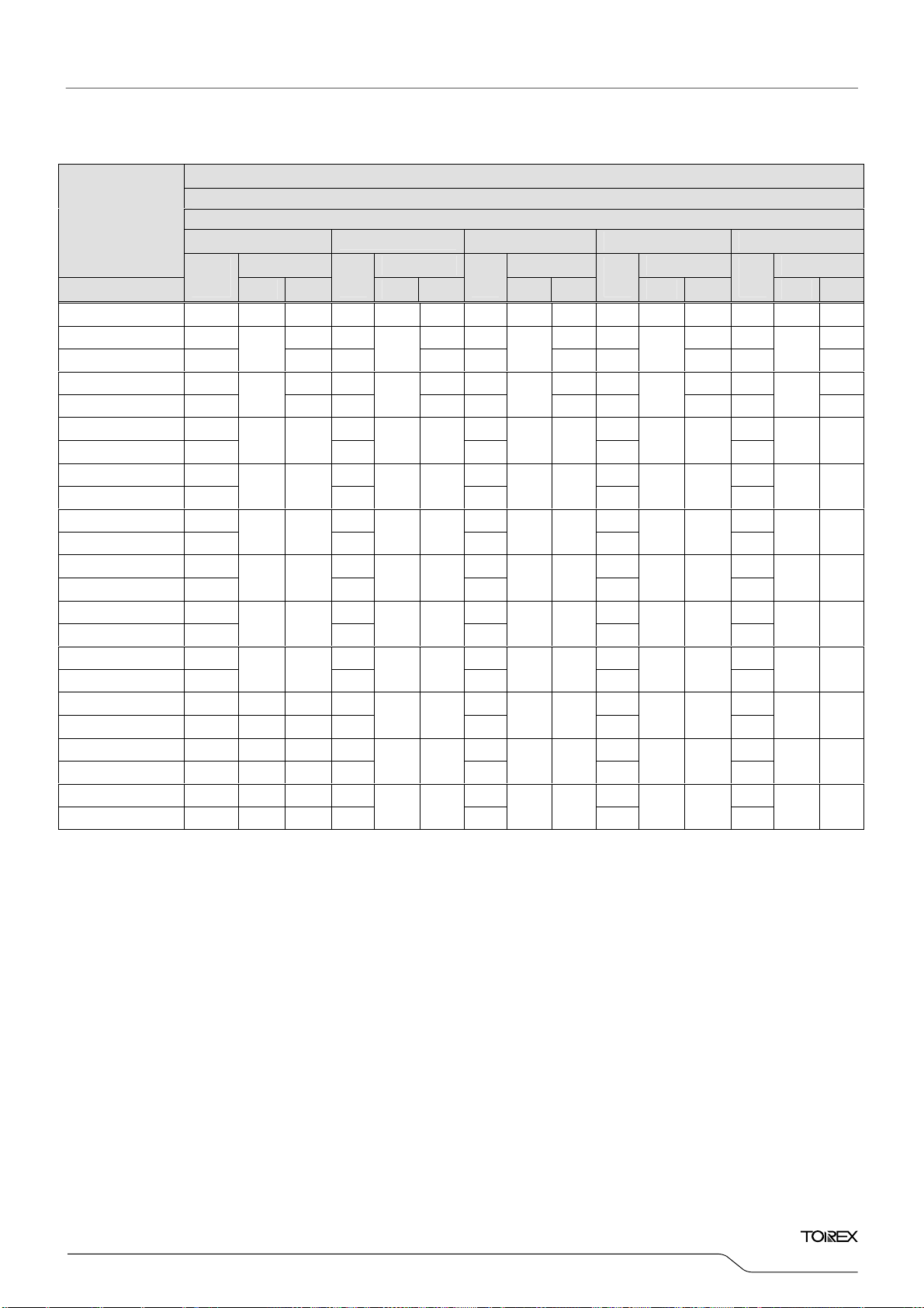
■OUTPUT VOLTAGE CHART
: Time that V
SS
* The electrical characteristics above are when the other channel is in stop mode.
(*11)
: Effective output voltage
: Specified output voltage
(*8)
-V
IN21
: The input voltage when VOUT1 appears as input voltage is gradually decreased.
: A voltage equal to 98% of the output voltage while maintaining an amply stabilized output voltage when V
≧3.0V at V
: A supply current at the V
NOMINAL OUTPUT
VOLTAGE (V)
V
ROUT(T)
△V
ROUT
(△Topr・V
I
LIM
I
SHORT
T
TSD
T
TSR
TSD-TTSR
R
DCHG
EN2H
EN2L
EN2H
EN2L
ROUT1
IN2=VBIAS
ROUT
t
SS
BIAS
(*9)
}
input to the V
becomes more than V
OUTPUT VOLTAGE (V)
MIN. MAX.
V
/
BIAS=VEN2
)
ROUT
Junction Temperature - 150 - ℃
Junction Temperature - 125 - ℃
- 25 - ℃
within the range V
within the range VIN≦V
IN
BIAS
E-0
V
ROUT
0.70 0.680 0.720
0.75 0.730 0.770
0.80 0.780 0.820
0.85 0.830 0.870
0.90 0.880 0.920
0.95 0.930 0.970
1.00 0.980 1.020
1.05 1.030 1.070
1.10 1.080 1.120
1.15 1.130 1.170
1.20 1.180 1.220
1.25 1.230 1.270
=3.6V, V
IN2=VROUT(T)
+0.3V , I
- 40℃≦ Topr ≦85℃
V
ROUT=VROUT(T)
V
BIAS=VEN2
V
BIAS=VEN2
V
BIAS
V
BIAS
V
=3.6V、V
BIAS
pin.
BIAS
pin providing for the output current (I
ROUT(E)
=3.6V, V
=3.6V, V
=3.6V, V
V
V
=6.0V, V
= V
IN2
V
ROUT=VROUT(T)
=3.6V,V
BIAS
=3.6V,V
BIAS
V
BIAS=VEN2
V
IN2=VROUT(T)
EN2=VSS,VIN2=VROUT(T)
IN2=VROUT(T)
V
EN2
BIAS –VROUT(T)
BIAS
×0.9V after the EN2 pin is input 0.75V as EN2 “H” level voltage.
IN2=VROUT(T)
IN2=VROUT(T)
=0V
V
ROUT
ROUT(T)
IN2=VROUT(T)
IN2=VROUT(T)
=6.0V,
+0.3V
=0V→3.6V
≧0.9V
×0.95,
+0.3V
+0.3V,
+0.3V, V
EN2
+0.3V 0.75 - 6.0
+0.3V - - 0.16
+0.3V、I
OUT
=30mA,
OUT
- ±100 - ppm/℃
400 - - mA
- 80 - mA
= VSS
290 430 610 Ω
-0.1 - 0.1
+0.3V -0.1 - 0.1
=1mA
) .
VROUT
NOMINAL OUTPUT
VOLTAGE (V)
V
100 - 410
BIAS
E-0
OUTPUT VOLTAGE (V)
V
ROUT
MIN. MAX.
ROUT(T)
1.30 1.280 1.320
1.35 1.330 1.370
1.40 1.380 1.420
1.45 1.430 1.470
1.50 1.480 1.520
1.55 1.530 1.570
1.60 1.580 1.620
1.65 1.630 1.670
1.70 1.680 1.720
1.75 1.730 1.770
1.80 1.780 1.820
V
V
μA ⑩
μA ⑩
μs ⑫
<3.0V at V
CIRCUIT
= V
IN2
⑩
⑩
⑩
⑩
⑩
⑩
⑩
⑩
⑩
BIAS,
11/49
XCM519 Series
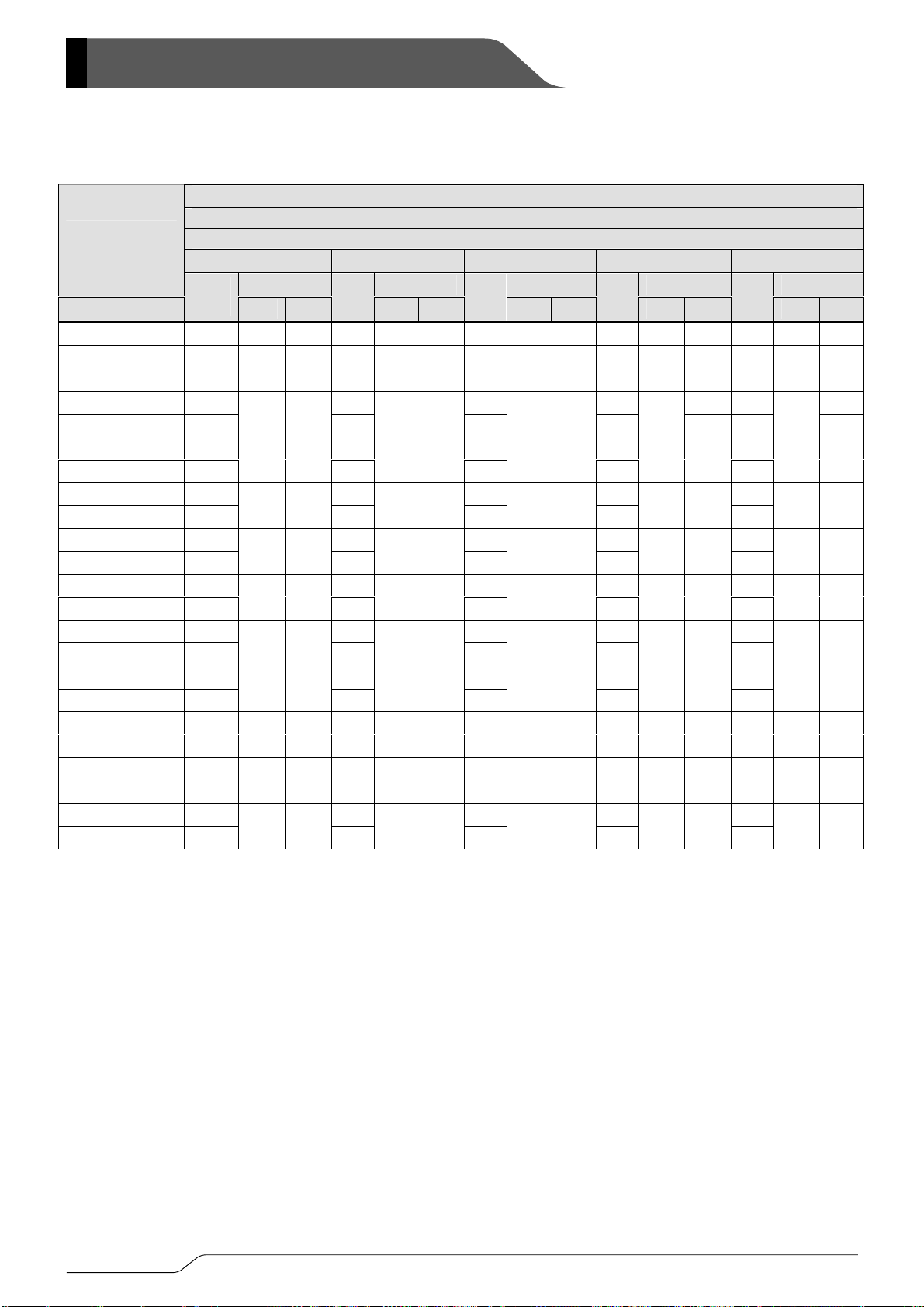
■DROPOUT VOLTAGE CHART
E-1
NOMINAL OUTPUT
VOLTAGE (V)
V
ROUT(T)
0.70
0.75
0.80
0.85
0.90
0.95
1.00
1.05
1.10
1.15
1.20
1.25
1.30
1.35
1.40
1.45
1.50
1.55
1.60
1.65
1.70
1.75
1.80
V
=3.0(V)
BIAS
(*1)
Vgs
(V)
2.30
2.25
2.20
2.15
2.10
2.05 2.35 2.65 3.25
Vdif (mV) Vdif (mV) Vdif (mV) Vdif (mV) Vdif (mV)
TYP. MAX.
40 300
250
41
200
150
42
100
43 68
2.00
1.95 2.25 2.55 3.15 3.95
46 72
1.90
1.85 2.15 2.45 3.05 3.85
48 75
1.80
1.75 2.05 2.35 2.95 3.75
51 81
1.70
1.65 1.95 2.25 2.85 3.65
54 87
1.60
1.55 1.85 2.15 2.75 3.55
57 92
1.50
1.45 61
1.40
63 97
1.35 67
1.30
70 113
1.25 74
1.20
79 154
94
104
131
V
=3.3(V)
BIAS
Vgs
(V)
TYP. MAX.
2.60
2.55
35 300
36
2.50
2.45
38
2.40
40 61
2.30
41 63
2.20
42 65
2.10
43 68
2.00
46 72
1.90
48 75
1.80
1.75 2.05 2.65 3.45
51 81
1.70
1.65 1.95 2.55 3.35
54 87
1.60
1.55 1.85 2.45 3.25
57 92
1.50
*1): Vgs is a Gate –Source voltage of the driver transistor that is defined as the value of V
DROPOUT VOLTAGE1 (mV)
Vdif1
V
=3.6(V) V
BIAS
Vgs
(V)
TYP. MAX.
33 300
34
34
250
200
150
100
2.90
2.85
2.80
2.75
2.70
35 56
2.60
36 58
2.50
38 59
2.40
40 61
2.30
41 63
2.20
42 65
2.10
43 68
2.00
46 72
1.90
48 75
1.80
250
200
150
100
BIAS
- V
Vgs
(V)
3.50
3.45
3.40
3.35
3.30
3.20
3.10
3.00
2.90
2.80
2.70
2.60
2.50
2.40
ROUT
=4.2(V) V
BIAS
TYP. MAX.
30 300
31
31
32
32 50
32 51
33 52
34 53
34 54
35 56
36 58
38 59
.
(T)
250
200
150
100
50
49
Vgs
(V)
4.30
4.25
4.20
4.15
4.10
4.05
4.00
3.90
3.80
3.70
3.60
3.50
3.40
3.30
3.20
=5.0(V)
BIAS
TYP. MAX.
27 300
28
28
28
29 45
29 46
29 47
30 47
30 48
31 48
31 49
32 49
250
200
150
100
50
44
12/49
X
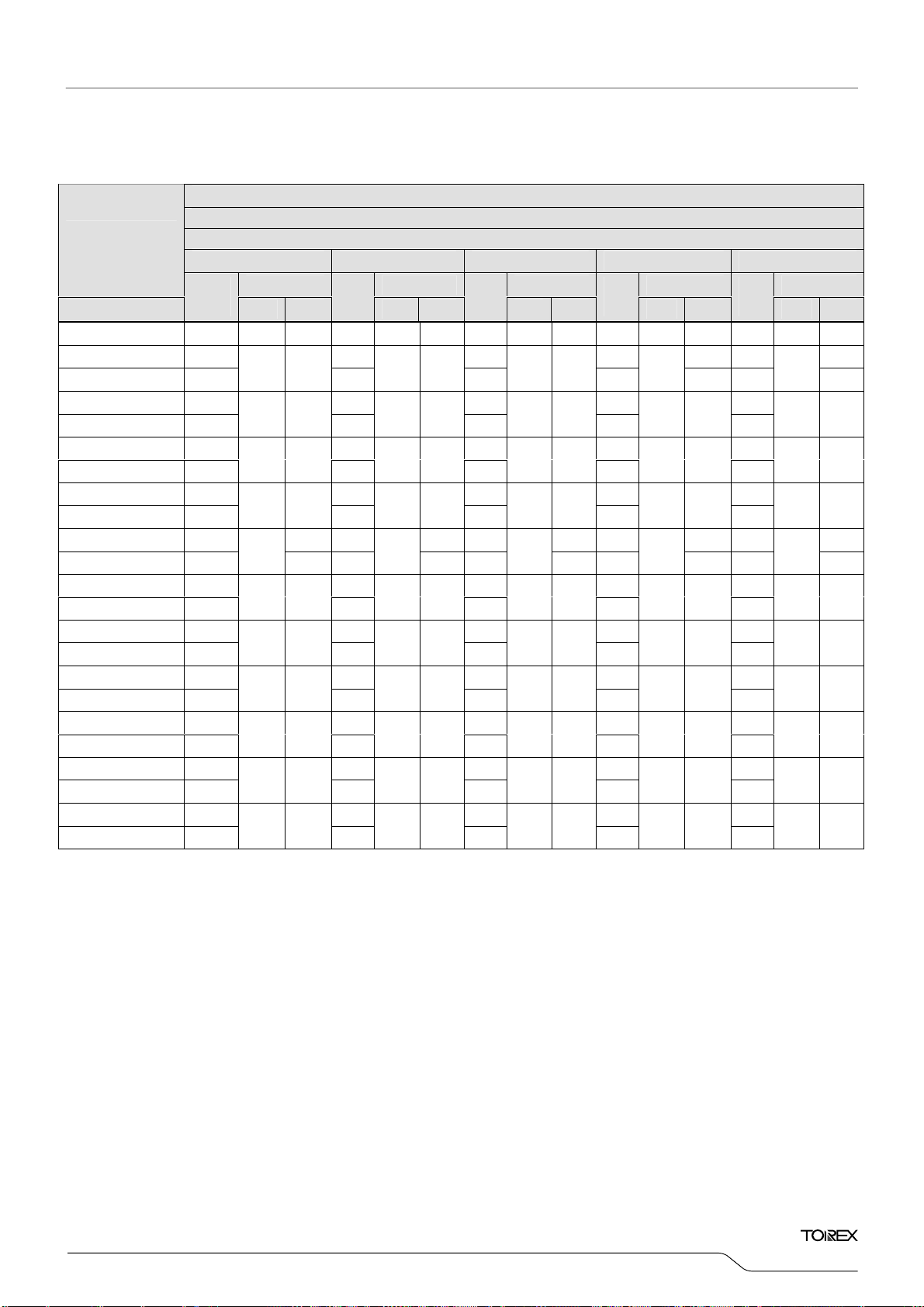
■DROPOUT VOLTAGE CHART (Continued)
E-2
DROPOUT VOLTAGE 2 (mV)
NOMINAL OUTPUT
VOLTAGE (V)
V
ROUT(T)
0.70
0.75
0.80
0.85
0.90
0.95
1.00
1.05
1.10
1.15
1.20
1.25
1.30
1.35
1.40
1.45
1.50
1.55
1.60
1.65
1.70
1.75
1.80
V
=3.3(V)
V
=3.0(V)
BIAS
(*1)
Vgs
(V)
2.30
2.25
2.20
2.15
2.10
2.05 2.35 2.65 3.25 4.05
Vdif (mV) Vdif (mV) Vdif (mV) Vdif (mV) Vdif (mV)
TYP MAX
81 300
250
85
200
150
88
131
90 139
2.00
1.95 2.25 2.55 3.15 3.95
96 146
1.90
1.85 2.15 2.45 3.05 3.85
101 154
1.80
1.75 2.05 2.35 2.95 3.75
108 170
1.70
1.65 1.95 2.25 2.85 3.65
115 179
1.60
1.55 1.85 2.15 2.75 3.55
122 192
1.50
1.45 129
1.40
135 206
1.35 145
1.30
154 248
1.25 165
1.20
175 353
197
223
293
BIAS
Vgs
(V)
TYP MAX
2.60
2.55
2.50
2.45
2.40
74 300
250
76
200
150
78
117
81 123
2.30
85 127
2.20
88 131
2.10
90 139
2.00
96 146
1.90
101 154
1.80
1.75 2.05 2.65 3.45
108 170
1.70
1.65 1.95 2.55 3.35
115 179
1.60
1.55 1.85 2.45 3.25
122 192
1.50
Vdif2
V
=3.6(V) V
BIAS
Vgs
(V)
TYP MAX
2.90
2.85
68 300
70
2.80
2.75
72
2.70
74 111
2.60
76 114
2.50
78 117
2.40
81 123
2.30
85 127
2.20
88 131
2.10
90 139
2.00
96 146
1.90
101 154
1.80
*1): Vgs is a Gate –Source voltage of the driver transistor that is defined as the value of V
250
200
150
110
BIAS
- V
Vgs
(V)
3.50
3.45
3.40
3.35
3.30
3.20
3.10
3.00
2.90
2.80
2.70
2.60
2.50
2.40
ROUT
=4.2(V) V
BIAS
TYP MAX
62 300
63
63
64 98
65 101
67 103
68 106
70 108
72 110
74 111
76 114
78 117
.
(T)
250
200
150
100
Vgs
(V)
4.30
4.25
4.20
4.15
4.10
4.00
3.90
3.80
3.70
3.60
3.50
3.40
3.30
3.20
CM519
Series
=5.0(V)
BIAS
TYP MAX
57 300
58
58
58 88
59 90
59 91
60 92
61 93
62 94
63 95
63 97
64 98
250
200
150
100
13/49
XCM519 Series
■DROPOUT VOLTAGE CHART (Continued)
E-3
NOMINAL OUTPUT
VOLTAGE (V)
V
VROUT(T)
0.70
0.75
0.80
0.85
0.90
0.95
1.00
1.05
1.10
1.15
1.20
1.25
1.30
1.35
1.40
1.45
1.50
1.55
1.60
1.65
1.70
1.75
1.80
V
=3.0(V)
BIAS
(*1)
Vgs
(V)
2.30
2.25
2.20
2.15
2.10
2.05
2.00
1.95 2.25 2.55 3.15 3.95
1.90
1.85 2.15 2.45 3.05 3.85
1.80
1.75 2.05 2.35 2.95 3.75
1.70
1.65 1.95 2.25 2.85 3.65
1.60
1.55 1.85 2.15 2.75 3.55
1.50
1.45 209
1.40
1.35 239
1.30
1.25 1.55 1.85 2.45 3.25
1.20
Vdif(mV) Vdif(mV) Vdif(mV) Vdif(mV) Vdif(mV)
TYP MAX
130 300
134
138 204
145 216
153 227
161 239
173 264
184 289
196 313
222 344
256 442
250
200
323
388
- -
V
=3.3(V)
BIAS
Vgs
(V)
TYP MAX
115 300
2.60
2.55
117
2.50
2.45 2.75 3.35 150 4.15 150
119 181
2.40
2.35 2.65 3.25 4.05
130 190
2.30
134 197
2.20
138 204
2.10
145 216
2.00
153 227
1.90
161 239
1.80
1.75 2.05 2.65 3.45
173 264
1.70
1.65 1.95 2.55 3.35
184 289
1.60
196 313
1.50
*1): Vgs is a Gate –Source voltage of the driver transistor that is defined as the value of V
DROPOUT VOLTAGE 3 (mV)
Vdif3
V
=3.6(V) V
BIAS
Vgs
(V)
TYP MAX
107 300
109
111 167
115 170
117 176
119 181
130 190
134 197
138 204
145 216
153 227
161 239
250
200
2.90
2.85
2.80
2.70
2.60
2.50
2.40
2.30
2.20
2.10
2.00
1.90
1.80
250
200
BIAS
- V
Vgs
(V)
3.50
3.45
3.40
3.30
3.20
3.10
3.00
2.90
2.80
2.70
2.60
2.50
2.40
ROUT
=4.2(V) V
BIAS
TYP MAX
95 300
96
97
98 151
101 153
105 155
107 159
109 163
111 167
115 170
117 176
119 181
.
(T)
Vgs
(V)
4.30
250
4.25
200
4.20
148 4.10
4.00
3.90
3.80
3.70
3.60
3.50
3.40
3.30
3.20
=5.0(V)
BIAS
TYP MAX
89 300
90
90
91 134
92 137
93 139
93 140
94 141
95 142
96 145
97 148
98 151
250
200
132
14/49
X
■DROPOUT VOLTAGE CHART (Continued)
E-4
DROPOUT VOLTAGE 4(mV)
NOMINAL OUTPUT
VOLTAGE (V)
V
VROUT(T)
0.70
0.75
0.80
0.85
0.90
0.95
1.00
1.05
1.10
1.15
1.20
1.25
1.30
1.35
1.40
1.45
1.50
1.55
1.60
1.65
1.70
1.75
1.80
V
=3.0(V) V
BIAS
(*1)
Vgs
(V)
2.30
2.25 2.55 2.85 3.45
2.20
2.15 2.45 2.75 3.35 4.15
2.10
2.05 2.35 2.65 3.25 4.05
2.00
1.95 2.25 2.55 3.15 3.95
1.90
1.85
1.80
1.75 2.05 2.35 2.95 3.75
1.70
1.65 1.95 2.25 2.85 3.65
1.60
1.55 1.85 2.15 2.75 3.55
1.50
1.45 1.75 2.05 2.65 3.45
1.40
1.35 1.65 1.95 2.55 3.35
1.30
1.25 1.55 1.85 2.45 3.25
1.20
Vdif(mV) Vdif(mV) Vdif(mV) Vdif(mV) Vdif(mV)
Vgs
TYP MAX
189 300
2.60
195 277
2.50
201 277
2.40
206 277
2.30
218 277
2.20
227
231
334
2.15
2.10
248 376
2.00
264 418
1.90
281 460
1.80
- -
1.70
- -
1.60
- -
1.50
(V)
BIAS
TYP MAX
=3.3(V) V
157 300
164 272
170 272
189 272
195 272
272
201
277
206 296
218 315
231 334
248 376
264 418
281 460
Vdif4
=3.6(V) V
BIAS
Vgs
(V)
TYP MAX
2.90
146 300
150 250
2.80
153 250
2.70
157 250
2.60
164 250
2.50
2.45
170
2.40
189 255
2.30
195 266
2.20
201 277
2.10
206 296
2.00
218 315
1.90
231 334
1.80
*1): Vgs is a Gate –Source voltage of the driver transistor that is defined as the value of V
250
248
BIAS
- V
Vgs
(V)
3.50
3.40
3.30
3.20
3.10
3.05
3.00
2.90
2.80
2.70
2.60
2.50
2.40
ROUT
=4.2(V) V
BIAS
TYP MAX
129 300
131
134 246
136 246
139 246
142
146 219
150 224
153 228
157 234
164 241
170 248
.
(T)
250
246
246
215
Vgs
(V)
4.30
4.25
4.20
4.10
4.00
3.90
3.85
3.80
3.70
3.60
3.50
3.40
3.30
3.20
CM519
Series
=5.0(V)
BIAS
TYP MAX
116 300
118
119 231
121 231
125 231
128
128 191
129 193
129 195
131 198
134 202
136 205
250
231
231
189
15/49

XCM519 Series
■TYPICAL APPLICATION CIRCUIT
● DC/DC BLOCK f
L : 1.5μH (NR3015 TAIIYO YUDEN)
CIN1 : 10μF (Ceramic)
CL1 : 10μF (Ceramic)
CBIAS : 1μF (Ceramic)
CIN2 : 1μF (Ceramic)
CL2 : 4.7μF (Ceramic)
DCOUT
VROUT
=3.0MHz
OSC
C
L1
1
2
EN1
3
C
C
4
IN2
5
L2
6
■OPERATIONAL EXPLANATION
L
DCOUT
AVSS
EN1 VIN1
VIN2
VSS2
VROUT EN2
PVSS
VBIAS
Lx
12
11
C
IN1
VIN
C
BIAS
EN2
NC
10
9
8
7
● DC/DC BLOCK f
L : 4.7μH (NR4018 TAIIYO YUDEN)
CIN1 : 10μF (Ceramic)
CL1 : 10μF (Ceramic)
CBIAS : 1μF (Ceramic)
CIN2 : 1μF (Ceramic)
CL2 : 4.7μF (Ceramic)
=1.2MHz
OSC
●DC/DC BLOCK
The DC/DC block of the XCM519 series consists of a reference voltage source, ramp wave circuit, error amplifier, PWM
comparator, phase compensation circuit, output voltage adjustment resistors, P-channel MOSFET driver transistor, N-channel
MOSFET switching transistor for the synchronous switch, current limiter circuit, UVLO circuit and others. (See the block
diagram above.)
The series ICs compare, using the error amplifier, the voltage of the internal voltage reference source with the feedback voltage
from the DCOUT pin through split resistors, R1 and R2. Phase compensation is performed on the resulting error amplifier
output, to input a signal to the PWM comparator to determine the turn-on time during PWM operation. The PWM comparator
compares, in terms of voltage level, the signal from the error amplifier with the ramp wave from the ramp wave circuit, and
delivers the resulting output to the buffer driver circuit to cause the Lx pin to output a switching duty cycle. This process is
continuously performed to ensure stable output voltage. The current feedback circuit monitors the P-channel MOS driver
transistor current for each switching operation, and modulates the error amplifier output signal to provide multiple feedback
signals. This enables a stable feedback loop even when a low ESR capacitor such as a ceramic capacitor is used ensuring
stable output voltage.
<Reference Voltage Source>
The reference voltage source provides the reference voltage to ensure stable output voltage of the DC/DC converter.
<Ramp Wave Circuit>
The ramp wave circuit determines switching frequency. The frequency is fixed internally and can be selected from 1.2MHz or
3.0MHz. Clock pulses generated in this circuit are used to produce ramp waveforms needed for PWM operation, and to
synchronize all the internal circuits.
<Error Amplifier>
The error amplifier is designed to monitor output voltage. The amplifier compares the reference voltage with the feedback
voltage divided by the internal split resistors, R1 and R2. When a voltage is lower than the reference voltage is fed back, the
output voltage of the error amplifier increases. The gain and frequency characteristics of the error amplifier output are fixed
internally to deliver an optimized signal to the mixer.
16/49

X
CM519
Series
■OPERATIONAL EXPLANATION (Continued)
<Current Limit>
The current limiter circuit of the XCM519 series monitors the current flowing through the P-channel MOS driver transistor
connected to the Lx pin, and features a combination of the current limit mode and the operation suspension mode.
① When the driver current is greater than a specific level, the current limit function operates to turn off the pulses from the Lx pin
at any given timing.
② When the P-channel MOS driver transistor is turned off, the limiter circuit is then released from the current limit detection
state.
③ At the next pulse, the P-channel MOS driver transistor is turned on. However, the P-channel MOS driver transistor is
immediately turned off in the case of an over current state.
④ When the over current state is eliminated, the IC resumes its normal operation.
The IC waits for the over current state to end by repeating the steps ① through ③. If an over current state continues for a
few ms and the above three steps are repeatedly performed, the IC performs the function of latching the OFF state of the
P-channel MOS driver transistor, and goes into operation suspension mode. Once the IC is in suspension mode, operations
can be resumed by either turning the IC off via the CE/MODE pin, or by restoring power to the V
does not mean a complete shutdown, but a state in which pulse output is suspended; therefore, the internal circuitry remains in
operation. The current limit of the XCM519 series can be set at 1050mA at typical. Besides, care must be taken when laying
out the PC Board, in order to prevent miss-operation of the current limit mode. Depending on the state of the PC Board, latch
time may become longer and latch operation may not work. In order to avoid the effect of noise, the board should be laid out
so that input capacitors are placed as close to the IC as possible.
Limit<#ms Limit>#ms
<Short-Circuit Protection>
The short-circuit protection circuit monitors the internal R1 and R2 divider voltage from the DCOUT pin. In case where
output is accidentally shorted to the Ground and when the FB point voltage decreases less than half of the reference
voltage (Vref) and a current more than the I
flows to the P-channel MOS driver transistor, the short-circuit protection
LIM
quickly operates to turn off and to latch the P-channel MOS driver transistor. In latch state, the operation can be resumed
by either turning the IC off and on via the EN1 pin, or by restoring power supply to the V
IN1
pin.
When sharp load transient happens, a voltage drop at the DCOUT pin is propagated to FB point through C
short circuit protection may operate in the voltage higher than 1/2 V
voltage.
OUT
<UVLO Circuit>
When the V
output caused by unstable operation of the internal circuitry. When the V
IN1 pin voltage becomes 1.4V or lower, the P-channel MOS driver transistor is forced OFF to prevent false pulse
pin voltage becomes 1.8V or higher, switching
IN1
operation takes place. By releasing the UVLO function, the IC performs the soft start function to initiate output startup
operation. The soft start function operates even when the V
IN pin voltage falls momentarily below the UVLO operating voltage.
The UVLO circuit does not cause a complete shutdown of the IC, but causes pulse output to be suspended; therefore, the
internal circuitry remains in operation.
pin. The suspension mode
IN
, as a result,
FB
17/49

XCM519 Series
■OPERATIONAL EXPLANATION (Continued)
<PFM Switch Current>
In the PFM control operation, until coil current reaches to a specified level (D
transistor on. In this case, on-time (t
) that the P-channel MOS driver transistor is kept on can be given by the following
ON
formula.
t
= L×IPFM (VIN1-V
ON
) →IPFM①
DCOUT
<PFM duty Limit>
In the PFM control operation, the PFM duty limit (D
) is set to 200% (TYP.). Therefore, under the condition that the duty
LIMT_PFM
increases (e.g. the condition that the step-down ratio is small), it’s possible for P-channel MOS driver transistor to be turned off
even when coil current doesn’t reach to IPFM. →IPFM②
<CL High Speed Discharge>
XCM519xC/ XCM519xD series can quickly discharge the electric charge at the output capacitor (CL) when a low signal to the CE
pin which enables a whole IC circuit put into OFF state, is inputted via the N-channel MOSFET switching transistor located
between the L
pin and the VSS pin. When the IC is disabled, electric charge at the output capacitor (CL) is quickly discharged so
X
that it may avoid application malfunction. Discharge time of the output capacitor (CL) is set by the CL auto-discharge resistance
(R) and the output capacitor (C
value (C
) as
L
). By setting time constant of a CL auto-discharge resistance value [R] and an output capacitor
L
τ(τ=C x R), discharge time of the output voltage after discharge via the N channel transistor is calculated by the following
formula.
V = V
DCOUT(T)
V : Output voltage after discharge
V
: Output voltage
DCOUT (T)
t: Discharge time
τ: C×R
C= Capacitance of Output capacitor (C
R= CL auto-discharge resistance
×e
-t /τ
or t = τLn (DCOUT(E) / V)
Output Voltage Dischage Characteristics
100
90
80
)
L
70
60
50
40
30
20
10
0
0 102030405060708090100
), the IC keeps the P-channel MOS driver
LIMIT_PFM
Rdischg
()
= 300Ω TYP
CL=10uF
CL=20uF
CL=50uF
Discharge Time t (ms)
18/49

X
CM519
Series
■OPERATIONAL EXPLANATION (Continued)
●Voltage Regulator BLOCK
The voltage divided by resistors R1 & R2 is compared with the internal reference voltage by the error amplifier. The N-channel
MOSFET which is connected to the V
is controlled & stabilized by a system of negative feedback.
V
pin is power supply pin for output voltage control circuit, protection circuit and CE circuit. When output current increase,
BIAS
the V
pin supplies output current also. V
BIAS
In order to obtain high efficient output current through low on-resistance, please take enough Vgs (=V
transistor. Output current triggers operation of constant current limiter and fold-back circuit, heat generation triggers operation of
thermal shutdown circuit, the driver transistor circuit is forced OFF when V
Further, the IC's internal circuitry can be shutdown via the EN2 pin's signal.
<Low ESR Capacitor>
With the XCM519 series, a stable output voltage is achievable even if used with low ESR capacitors, as a phase compensation
circuit is built-in. The output capacitor (C
compensation. Values required for the phase compensation are as the table below.
For a stable power input, please connect an bias capacitor (C
connect an input capacitor (CIN2) of 1.0μF between the VIN2 pin and the VSS pin. In order to ensure the stable phase
compensation while avoiding run-out of values, please use the capacitor (C
temperature too much. The table below shows recommended values of C
VOLTAGE
0.7V~1.8V C
pin is then driven by the subsequent output signal. The output voltage at the V
ROUT
pin is connected to a driver transistor and provides output current.
IN2
– V
BIAS
ROUT (T)
or V
voltage goes lower than UVLO voltage.
IN2
pin and VSS pin to obtain stable phase
ROUT
pin and the VSS pin. Also, please
BIAS
, C
, CL2 ) which does not depend on bias or
IN2
Figure 1: XC6601B Series
) should be connected as close to V
L2
) of 1.0μF between the V
BIAS
BIAS
BIAS
, CIN, CL.
BIAS
BIAS CAPACITOR INPUT CAPACITOR OUTPUT CAPACITOR NOMINAL
C
C
BIAS
=1.0μF C
BIAS
Recommended Values of C
CL2
IN2
=1.0μF CL2=4.7μF
IN2
BIAS, CIN2, CL2
pin
ROUT
) of the driver
19/49

XCM519 Series
■OPERATIONAL EXPLANATION (Continued)
<Soft-start>
With the XCM519, the inrush current from V
The soft-start time is optimized to 240μA (TYP.) at V
V
from the time when CE H threshold 0.75V is input to the CE pin.
ROUT (E)
(mA)
RUSH
I
Inrush Current
Figure2: Example of the inrush current wave form at IC start-up. Figure3: Timing chart at IC start-up
<
CL High Speed Auto-Discharge>
XCM519 series can quickly discharge the electric charge at the output capacitor (CL) when a low signal to the EN2 pin which
enables a whole IC circuit put into OFF state, is inputted via the N-channel transistor located between the V
V
SS pin. When the IC is disabled, electric charge at the output capacitor (CL) is quickly discharged so that it could avoids
malfunction. At that time, CL discharge resistance is depended on a bias voltage. Discharge time of the output capacitor (CL)
is set by the C
L auto-discharge resistance (R) and the output capacitor (CL). By setting time constant of a CL auto-discharge
resistance value [R] and an output capacitor value (CL) as τ(τ=C x R), the output voltage after discharge via the N channel
transistor is calculated by the following formulas.
V = V
V : Output voltage after discharge, V
τ: C
x e –t/τ, or t=τln(V
ROUT(E)
L auto-discharge resistance R×Output capacitor (CL) value C
ROUT(E)
/ V
ROUT(E)
<Current Limit, Short-Circuit Protection>
The XCM519 series’ fold-back circuit operates as an output current limiter and a short protection of the output pin. When the
load current reaches the current limit level, the fixed current limiter circuit operates and output voltage drops. When the output
pin is shorted to the V
level, current flows about 50mA.
SS
<Thermal Shutdown Circuit (TSD) >
When the junction temperature of the built-in driver transistor reaches the temperature limit level (150℃ TYP.), the thermal
shutdown circuit operates and the driver transistor will be set to OFF. The IC resumes its operation when the thermal shutdown
function is released and the IC’s operation is automatically restored because the junction temperature drops to the level of the
thermal shutdown release temperature (135℃ TYP.).
<Under Voltage Lock Out (UVLO) >
When the V
pin voltage drops below 2.0V (TYP.) or V
BIAS
forced OFF by UVLO function to prevent false output caused by unstable operation of the internal circuitry. When the V
voltage rise at 2.2V (TYP.) or the V
pin voltage rises at 0.4V (TYP.), the UVLO function is released. The driver transistor is
IN2
turned in the ON state and start to operate voltage regulation.
IN2
to V
(V)
EN2 Input Voltage
for charging CL at start-up can be reduced and makes the V
ROUT
=1.2V internally. Soft-start time is defined as the V
ROUT
EN2
V
)
: Output voltage, t: Discharge time,
pin voltage drops below 0.4V (TYP.), the output driver transistor is
IN2
reaches 90% of
ROUT
pin and the
ROUT
stable.
IN2
BIAS
pin
20/49

X
CM519
Series
■OPERATIONAL EXPLANATION (Continued)
<EN2 Pin>
The IC internal circuitry can be shutdown via the signal from the EN2 pin with the XCM519 series. In shutdown mode, output at
the V
resistor is connected in parallel to R1 and R2 while the power supply is applied to the V
pin reaches the V
pin will be pulled down to the VSS level via R1 & R2. However, as for the XCM519 series, the CL auto-discharge
ROUT
pin. Therefore, time until the VROUT
IN2
level becomes short.
SS
The EN2 pin of XCM519 has pull-down circuitry so that EN2 input current increase during IC operation. The EN2 pin of XCM519
does not have pull-down circuitry so that logic is not fixed when the CE pin is open. If the EN2 pin voltage is taken from V
BIAS
pin or VSS pin then logic is fixed and the IC will operate normally. However, supply current may increase as a result of through
current in the IC's internal circuitry when medium voltage is input.
■NOTE ON USE
When the DC/DC converter and the VR are connected as V
IN1=VBIAS
1. When the DC/DC load is changed drastically during a light load of the VR, a fluctuation may happen in tenths of mV. This
value can be reduced by increasing C
load capacitance at the DC/DC in order to reduce a voltage drop during load
L1
transient.
2. It is recommended that both C
立ち上がり 立下り
1ch:DC/DC VOUT:50mV/div
2ch:VR VOUT:50mV/div
4ch:VR IOUT:200mA/div
20μs/div
IN1
and C
are connected to each pin separately. When one capacitor is used instead of
BIAS
the two, this capacitor should be placed in 10μF or more as close as the VIN1 and the PGND (AGND) pins of the DC/DC
circuit. Please ensure it by testing on the actual product design.
3. It is recommended that both C
and C
L1
are connected to each pin separately. When one capacitor is used instead of the
IN2
two, this capacitor should be selected in 4.7μF or bigger. Please ensure it by testing on the actual product design.
4. C
of the VR is recommended 4.7μA. When larger value is used in CL2, the larger value is also used in C
L2
proportional. Please be noted that when C
capacitance of the VR is getting large, an inrush current increases at VR
L2
start-up, DC/DC short circuit protection starts to operate, as a result, the IC may happen to stop.
DCOUT(1V/div)
IIN2(500mA/div)
VROUT(1V/div)
EN2(5V/div)
* VR inrush current I
start, as a result, the IC may happen to stop.
The left waver forms are taken at C
contrast to the recommended 4.7μF).
However, it improves when C
, V
DCOUT=VIN2
, the following points should be noted.
1ch:DC/DC VOUT:50mV/div
2ch:VR VOUT:50mV/div
4ch:VR IOUT:200mA/div
50μs/div
makes DC/DC short-circuit protection to
IN2
=10μ, CL2=10μF(in
L1
=20μF.
L1
L1
as in
50us/div
21/49

XCM519 Series
■NOTE ON USE (Continued)
5. When the input-output voltage differential is small in the DC/DC converter and heavy load condition, a duty cycle is getting
large and keeps the 100% duty cycle in a several period cycles. At the time of duty cycle transition to 100% or from 100%,
noise may appear on the voltage regulator output. Please evaluate this on the actual design board when the condition is
in small input-output voltage differential and heavy load.
6. When the load is changed at the DC/DC converter, ringing may happen in some load conditions of DC/DC and VR at the
timing of turn on and turn off. The ringing can be reduced by increasing C
between V
and V
IN1
BIAS
pins.
7. In order to turn off the input voltage, the EN2 pin should be turned off first. If the input voltage is turned off with keeping VR
operation, the VROUT voltage goes up instantaneously as a result of the VR bias voltage transient.
VIN(5V/div)
DCOUT(500mV/div)
VROUT(500mV/div)
8. When the DCOUT pin is connected to the V
and EN2 should be started up 10μs later than V
200us/div
pin and the bias voltage (V
IN2
. If EN1 and EN2 is turned on within 10μs, inrush current like 1A may
BIAS
happen which result in starting the DC/DC short-circuit protection.
9. It is recommended to test this in the actual product design board.
<DC/DC BLOCK>
1. The XCM519 series is designed for use with ceramic output capacitors. If, however, the potential difference is too large
between the input voltage and the output voltage, a ceramic capacitor may fail to absorb the resulting high switching
energy and oscillation could occur on the output. If the input-output potential difference is large, connect an electrolytic
capacitor in parallel to compensate for insufficient capacitance.
2. Spike noise and ripple voltage arise in a switching regulator as with a DC/DC converter. These are greatly influenced by
external component selection, such as the coil inductance, capacitance values, and board layout of external components.
Once the design has been completed, verification with actual components should be done.
3. As a result of input-output voltage and load conditions, oscillation frequency goes to 1/2, 1/3, and continues, then a ripple
may increase.
4. When input-output voltage differential is large and light load conditions, a small duty cycle comes out. After that, 0%duty
cycle may continue in several periods.
5. When input-output voltage differential is small and heavy load conditions, a large duty cycle comes out and may
continues100% duty cycle in several periods.
6. With the IC, the peak current of the coil is controlled by the current limit circuit. Since the peak current increases when
dropout voltage or load current is high, current limit starts operation, and this can lead to instability. When peak current
becomes high, please adjust the coil inductance value and fully check the circuit operation. In addition, please calculate
the peak current according to the following formula:
Ipk = (V
IN1-VDCOUT
)× OnDuty /(2×L×f
OSC
) + I
OUT
L: Coil Inductance Value
f
: Oscillation Frequency
OSC
capacitance or placing a resistor over 10kΩ
IN1
) is taken from the other power supply, EN1
BIAS
22/49

X
CM519
Series
■NOTE ON USE (Continued)
7. When the peak current which exceeds limit current flows within the specified time, the built-in P-channel MOS driver
transistor turns off. During the time until it detects limit current and before the built-in P-channel MOS driver transistor can
be turned off, the current for limit current flows; therefore, care must be taken when selecting the rating for the external
components such as a coil.
Care must be taken when laying out the PC Board, in order to prevent misoperation of the current limit mode. Depending
8.
on the state of the PC Board, latch time may become longer and latch operation may not work. In order to avoid the effect
of noise, the board should be laid out so that input capacitors are placed as close to the IC as possible.
9. Use of the IC at voltages below the recommended voltage range may lead to instability.
10. This IC should be used within the stated absolute maximum ratings in order to prevent damage to the device.
11. When the IC is used in high temperature, output voltage may increase up to input voltage level at no load because of the
leak current of the P-channel MOS driver transistor.
12. The current limit is set to 1350mA (MAX.) at typical. However, the current of 1350mA or more may flow. In case that the
current limit functions while the DCOUT pin is shorted to the GND pin, when P-channel MOS driver transistor is ON, the
potential difference for input voltage will occur at both ends of a coil. For this, the time rate of coil current becomes large.
By contrast, when N-channel MOS switching transistor is ON, there is almost no potential difference at both ends of the coil
since the DCOUT pin is shorted to the GND pin. Consequently, the time rate of coil current becomes quite small.
According to the repetition of this operation, and the delay time of the circuit, coil current will be converged on a certain
current value, exceeding the amount of current, which is supposed to be limited originally. Even in this case, however,
after the over current state continues for several ms, the circuit will be latched. A coil should be used within the stated
absolute maximum rating in order to prevent damage to the device.
①Current flows into P-channel MOS driver transistor to reach the current limit (I
LIM).
②The current of ILIM or more flows since the delay time of the circuit occurs during from the detection of the current limit to
OFF of P-channel MOS driver transistor.
③Because of no potential difference at both ends of the coil, the time rate of coil current becomes quite small.
④Lx oscillates very narrow pulses by the current limit for several ms.
⑤The circuit is latched, stopping its operation.
13. In order to stabilize V
②
①
LX
ILIM
IL X
’s voltage level and oscillation frequency, we recommend that a by-pass capacitor (CIN) be
IN1
③
Dela y
④
Limit > # mS
ms
⑤
connected as close as possible to the VIN1 & VSS pins.
14. High step-down ratio and very light load may lead an intermittent oscillation.
15. During PWM / PFM automatic switching mode, operating may become unstable at transition to continuous mode.
Please verify with actual parts.
<External Components>
23/49

XCM519 Series
■NOTE ON USE (Continued)
16. Please note the inductance value of the coil. The IC may enter unstable operation if the combination of ambient temperature,
setting voltage, oscillation frequency, and L value are not adequate.
In the operation range close to the maximum duty cycle, The IC may happen to enter unstable output voltage operation even
if using the L values listed below.
<Regulator BLOCK>
1. Where wiring impedance is high, operations may become unstable due to noise and/or phase lag depending on output
current. Please keep the resistance low between V
2. Please wire the bias capacitor (C
3. Capacitance values of these capacitors (C
temperature. Care shall be taken for capacitor selection to ensure stability of phase compensation from the point of ESR
influence.
4. In case of the output capacitor more than CL=22μF is used, ringing of input current occurs when rising time.
5. V
and EN2 should be applied at least 10μs after the bias voltage V
IN2
If V
and EN2 are applied within 10μs, inrush current like 1A may occurs.
IN2
●Instructions of pattern layouts
1. Please use this IC within the stated absolute maximum ratings. The IC is liable to malfunction should the ratings be
exceeded.
2. In order to stabilize V
C
BIAS・CL1・CL2
3. Please mount each external component as close to the IC as possible.
4. Wire external components as close to the IC as possible and use thick, short connecting traces to reduce the circuit
impedance.
5. VSS(AGND・PGND・VSS)ground wiring is recommended to get large area. The IC may goes into unstable operation as a
result of VSS voltage level fluctuation during the switching.
6. This series’ internal driver transistors bring on heat because of the output current (I
transistors.
IN1・VIN2・VBIAS
) be connected as close as possible to the V
), input capacitor (C
BIAS
BIAS, CIN2, CL2
・DCOUT・V
●The Range of L Value
f
<External Components>
, V
BIAS
and VSS wiring in particular.
IN2
) and the output capacitor (CL2) as close to the IC as possible.
IN2
V
OSC
3.0MHz
1.2MHz
*When a coil less value of 4.7 μ H is used at
=1.2MHz or when a coil less value of 1.5μH is
f
OSC
used at f
reach the current limit ILMI. In this case, it may
happen that the IC can not provide 600mA output
current.
0.8V<V
=3.0MHz, peak coil current more easily
OSC
L Value
OUT
<4.0V 1.0μH~2.2μH
OUT
V
≦2.5V 3.3μH~6.8μH
OUT
2.5V<V
4.7μH~6.8μH
OUT
) are decreased by the influences of bias voltage and ambient
reaches the requested voltage.
BIAS
voltage level, we recommend that a by-pass capacitor (C
ROUT
IN1・VIN2・VBIAS
・DCOUT・V
and GND・VSS pins.
ROUT
) and ON resistance of driver
OUT
IN1・CIN2
・
AGND
EN1
VIN2
VSS
24/49
DCOUT
CIN3
VROUT
L
Lx
L
CL1
IC
CL2
CIN2
EN2
Front Back
PGND
Ceramic Capacitor
CIN1
Inductor
VBIAS VIN1

X
■TEST CIRCUITS
< Circuit No.1 >
A
CIN
※ External Components
L : 1.5μH(NR3015) 3.0MHz
4.7μH(NR4018) 1.2MHz
CIN : 4.7μF(ceramic)
CL :10μF(ceramic)
VIN1
EN1
AGND PGND
VBIAS
VIN2
EN2
DCOUT
VROUT
< Circuit No.3 >
1μF
VIN1
EN1
AGND PGND
VBIAS
VIN2
EN2
DCOUT
VROUT
< Circuit No.5 >
1μF
ICEH
A
ICEL
VIN1
EN1
AGND PGND
VBIAS
VIN2
EN2
< Circuit No.7 >
1uF
VIN1
EN1
AGND PGND
DCOUT
VBIAS
VIN2
EN2
VROUT
< Circuit No.9 >
A
CIN
VIN1
EN1
AGND PGND
VBIAS
VIN2
EN2
DCOUT
VROUT
Lx
Lx
DCOUT
VROUT
Lx
Lx
Lx
Wave Form Measure Point
L
CL
Wave Form Measure Point
Rpulldown
200Ω
ILeakH
A
ILeakL
Wave Form Measure Point
Ilat
Rpulldown
1Ω
CM519
Series
< Circuit No.2 >
DCOUT
VROUT
DCOUT
VROUT
DCOUT
VROUT
DCOUT
VROUT
Lx
Lx
100mA
V
ILx
A
Wave Form Measure Point
ILIM
V
Lx
Lx
A
V
1uF
VIN1
EN1
AGND PGND
VBIAS
VIN2
EN2
< Circuit No.4 >
VIN1
1μF
EN1
AGND PGND
VBIAS
VIN2
EN2
< Circuit No.6 >
VIN1
1μF
EN1
AGND PGND
VBIAS
VIN2
EN2
< Circuit No.8 >
VIN1
1uF
EN1
AGND PGND
VBIAS
VIN2
EN2
25/49

)
XCM519 Series
■TEST CIRCUITS (Continued
<CircuitNo.10>
V
A
A
V
A
Waveform
measure
V
CBIAS 1.0uFCIN2 1.0uF
CBIAS
1.0uFCIN2
SW3 SW4
CBIAS
1.0uFCIN2
SW1
SW2
V
V
V
<CircuitNo.11>
SW1
V
<CircuitNo.12>
V
* For the timing chart, please refer to <Soft-start> on page 20.
VIN1
EN1
AGND PGND
VBIAS
VIN2
EN2
VSS
VIN1
EN1
AGND PGND
VBIAS
VIN2
EN2
1.0uF
1.0uF
VSS
VIN1
EN1
AGND PGND
VBIAS
VIN2
EN2
VSS
DCOUT
VROUT
DCOUT
VROUT
DCOUT
VROUT
Lx
A
4.7uF
CL2
SW2
V
Lx
A
4.7uF
CL2
V
Lx
Waveform
RL
measure
A
4.7uF
CL2
V
RL
26/49

X
)
)
■TYPICAL PERFORMANCE CHARACTERISTICS
●1ch:DC/DC Block
(1) Efficiency vs. Output Current
DCOUT=1.8V,1.2MHz
L=4.7μH(NR4018), C
PWM/PFM A utomatic Switching Control
100
90
80
70
60
50
40
Efficency:EFF I(%
30
20
10
0
VIN= 4.2V
3.6V
0.1 1 10 100 1000
Output Cur rent:IOUT(mA)
(2) Output Voltage vs. Output Current
DCOUT=1.8V,1.2MHz DCOUT=1.8V,3.0MHz
L=4.7μH(NR4018), C
2.1
DCOUT=1.8V,3.0MHz
=10μF, CL1=10μF L=1.5μH(NR3015), C
IN1
PWM/PFM A utomatic Sw itching Contr ol
100
90
80
70
PWM Control
VIN= 4.2V
3.6V
=10μF, CL1=10μF L=1.5μH(NR3015), C
IN1
60
50
40
Effic ency :EFFI(%
30
20
10
0
0.1 1 10 100 1000
2.1
VIN= 4.2V
3.6V
Output Cur rent:IOUT(mA)
=10μF, CL1=10μF
IN1
PWM Control
VIN= 4.2V
3.6V
=10μF, CL1=10μF
IN1
CM519
Series
2.0
1.9
1.8
1.7
Output Voltage:Vout(V)
1.6
1.5
0.1 1 10 100 1000
PWM/PFM Automatic Sw itching Control
VIN=4.2V,3.6V
PWM Con tr ol
Output Cur rent:IOUT(mA)
(3) Ripple Voltage vs. Output Current
DCOUT=1.8V,1.2MHz
L=4.7μH(NR4018), C
100
80
60
PWM Control
40
VIN=4.2V,3.6V
Ripple Voltage:Vr(mV)
20
PWM/PFM A utomatic
Sw itc hing Control
VIN=4.2V
3.6V
2.0
1.9
1.8
1.7
Output Voltage:Vout(V)
1.6
1.5
0.1 1 10 100 1000
PWM/PFM Automatic Sw itching Contr ol
PWM Control
Output Cur rent:IOUT(mA)
DCOUT=1.8V,3.0MHz
=10μF, CL1=10μF L=1.5μH(NR3015), C
IN1
100
80
60
40
Ripple Voltage:Vr(mV)
20
PWM Control
VIN=4.2V,3.6V
PWM/PFM A utomatic
Sw itc hing Control
VIN=4.2V
3.6V
VIN=4.2V,3.6V
=10μF, CL1=10μF
IN1
0
0.1 1 10 100 1000
Output Cur rent:IOUT(mA)
0
0.1 1 10 100 1000
Output Cur rent:IOUT(mA)
27/49

)
)
XCM519 Series
■TYPICAL PERFORMANCE CHARACTERISTICS (Continued)
(4) Oscillation Frequency vs. Ambient Temperature
DCOUT=1.8V,1.2MHz
L=4.7μH(NR4018), C
1.5
1.4
1.3
1.2
1.1
1.0
0.9
Oscillation Frequency : FOSC(MHz)
0.8
-50 -25 0 25 50 75 100
VIN=3.6V
Ambient Temperature: Ta (℃)
(5) Supply Current vs. Ambient Temperature
DCOUT=1.8V,1.2MHz DCOUT=1.8V,3.0MHz
DCOUT=1.8V,3.0MHz
=10μF, CL1=10μF L=1.5μH(NR3015), C
IN1
3.5
3.4
3.3
3.2
3.1
3.0
2.9
2.8
2.7
Oscillation Frequency : FOSC(MHz)
2.6
2.5
-50 -25 0 25 50 75 100
VIN=3.6V
Ambient Temperature: Ta (℃)
=10μF, CL1=10μF
IN1
40
35
30
25
20
15
10
Supply Current : IDD (μA
5
0
-50 -25 0 25 50 75 100
VIN=4.0V
Ambient Temperature: Ta (℃)
VIN=6.0V
40
35
30
25
20
15
10
Supply Current : IDD ( μA
5
0
-50-25 0 255075100
VIN=4.0V
Ambient Temperature: Ta (℃)
VIN=6.0V
(6) Output Voltage vs. Ambient Temperature (7) UVLO Voltage vs. Ambient Temperature
DCOUT=1.8V,3.0MHz
2.1
2.0
1.9
1.8
VIN=3.6V
DCOUT=1.8V,3.0MHz
1.8
EN=VIN
1.5
1.2
0.9
EN=VIN EN=VIN
CE=V IN
1.7
Output Voltage : VOUT (V)
1.6
1.5
-50 -25 0 25 50 75 100
Ambient Temperature: Ta (℃)
0.6
UVLO Voltage : UVLO (V)
0.3
0.0
-50 -25 0 25 50 75 100
Ambient Temperature: Ta (℃)
28/49

X
)
)
)
■TYPICAL PERFORMANCE CHARACTERISTICS (Continued)
(8) EN "H" Voltage vs. Ambient Temperature (9)EN" L" Voltage vs. Ambient Temperature
DCOUT=1.8V,3.0MHz
1.0
0.9
0.8
0.7
0.6
0.5
0.4
0.3
CE "H" Voltage : VCEH (V
0.2
0.1
0.0
-50 -25 0 25 50 75 100
VIN=5.0V
VIN=3.6V
Ambient Temperature: Ta (℃)
(10) Soft Start Time vs. Ambient Temperature
DCOUT=1.8V,3.0MHz DCOUT=1.8V,3.0MHz
L=4.7μH(NR4018), CIN1=10μF, CL1=10μF L=1.5μH(NR3015), CIN1=10μF, CL1=10μF
DCOUT=1.8V,3.0MHz
1.0
0.9
0.8
0.7
0.6
0.5
0.4
0.3
CE "L" Voltage : VCEL (V)
0.2
0.1
0.0
-50 -25 0 25 50 75 100
VIN=5.0V
VIN=3.6V
Ambient Temperature: Ta (℃)
CM519
Series
5
4
3
2
Soft Start Time : TSS (ms
1
0
-50-250 255075100
VIN=3.6V
Ambient Temperature: Ta (℃)
5
4
3
2
Soft Start Time : TSS (ms
1
0
VIN=3.6V
-50 -25 0 25 50 75 100
Ambient Temperature: Ta (℃)
(11) "Pch / Nch" Driver on Resistance vs. Input Voltage
DCOUT=1.8V,3.0MHz
1.0
0.9
0.8
0.7
0.6
0.5
0.4
0.3
0.2
Lx SW ON Res istance:RLx H,RLxL (Ω)
0.1
0.0
0123456
Input Voltage : VIN ( V)
Nch on Resistance
Pch on Resistanc e
29/49

A
A
XCM519 Series
■TYPICAL PERFORMANCE CHARACTERISTICS (Continued)
(12) XCM519xC/ XCM519xD Rise Wave Form
DCOUT=1.2V,1.2MHz DCOUT=3.3V,3.0MHz
L=4.7μH (NR4018), CIN1=10μF, CL 1=1 0μF
L=1.5μH (NR3015), CIN1=10μF, CL 1=1 0μF
VIN1=5.0V
IOUT=1.0m
VOUT:0.5V/div
VOUT:1.0V/div
100μs/div
(13) XCM519xC/ XCM519xD Soft-Start Time vs. Ambient Temperature
DCOUT=1.2V,1.2MHz DCOUT=3.3V,3.0MHz
L=4.7μH(NR4018), CIN1=10μF, CL1=10μF L=1.5μH(NR3015), CIN1=10μF, CL1=10μF
500
400
300
200
100
VIN=5.0V
IOUT=1.0 mA
Soft Start Time :TSS (μs)
500
400
300
200
VIN=5.0V
Soft Start Time :TSS (μs)
IOUT=1.0 mA
100
VIN1=5.0V
IOUT=1.0m
EN:0.0V⇒1.0V EN:0.0V⇒1.0V
100μs/div
0
-50 -25 0 25 50 75 100
Ambient Temperature: Ta(℃)
0
-50 -25 0 25 50 75 100
Ambient Temperature: Ta(℃)
(14) XCM519xC/ XCM519xD CL Discharge Resistance vs. Ambient Temperature
DCOUT=3.3V,3.0MHz
600
500
400
300
200
CL Discharge Resistance: (Ω)
100
-50 -25 0 25 50 75 100
Ambient Temperature: Ta (℃)
VIN=6.0V
VIN=4.0V
30/49

X
■TYPICAL PERFORMANCE CHARACTERISTICS (Continued)
(15) Load Transient Response
DCOUT=1.2V,1.2MHz(PWM/PFM Automatic Switching Control)
L=4.7μH(NR4018), C
=3.6V, EN1=V
V
IN1
I
=1mA → 100mA I
OUT
1ch : I
V
: 50mV/div V
OUT
=100mA → 1mA I
I
OUT
1ch : I
: 50mV/div V
V
OUT
1ch : I
OUT
2ch 2ch
1ch : I
OUT
2ch 2ch
=10μF(ceramic), CL1=10μF(ceramic), Topr=25℃
IN1
IN1
50μs/div 50μs/div
200μs/div 200μs/div
=1mA → 300mA
OUT
OUT
: 50mV/div
OUT
=300mA → 1mA
OUT
OUT
: 50mV/div
OUT
CM519
Series
31/49

XCM519 Series
■TYPICAL PERFORMANCE CHARACTERISTICS (Continued)
(15) Load Transient Response (Continued)
DCOUT=1.2V,1.2MHz(PWM Control)
L=4.7μH(NR4018), C
=3.6V, EN1=V
V
IN1
I
=1mA → 100mA I
OUT
1ch: I
1ch: I
OUT
2ch 2ch
V
: 50mV/div V
OUT
=100mA → 1mA I
I
OUT
1ch: I
1ch: I
OUT
2ch 2ch
: 50mV/div V
V
OUT
=10μF(ceramic), CL1=10μF(ceramic), Topr=25℃
IN1
IN1
50μs/div 50μs/div
200μs/div 200μs/div
=1mA → 300mA
OUT
OUT
: 50mV/div
OUT
=300mA → 1mA
OUT
OUT
: 50mV/div
OUT
32/49

X
■TYPICAL PERFORMANCE CHARACTERISTICS (Continued)
(15) Load Transient Response (Continued)
DCOUT
L=1.5μH(NR3015), C
V
I
OUT
V
IOUT=100mA → 1mA IOUT=300mA → 1mA
V
=1.8V,3.0MHz(PWM/PFM Automatic Switching Control)
T
=10μF(ceramic), CL1=10μF(ceramic),Topr=25℃
IN1
=3.6V, EN=V
IN1
IN1
=1mA → 100mA I
1ch : I
1ch : I
OUT
2ch 2ch
: 50mV/div V
OUT
50μs/div 50μs/div
1ch : I
1ch : I
OUT
2ch 2ch
: 50mV/div V
OUT
200μs/div 200μs/div
=1mA → 300mA
OUT
OUT
: 50mV/div
OUT
OUT
: 50mV/div
OUT
CM519
Series
33/49

XCM519 Series
■TYPICAL PERFORMANCE CHARACTERISTICS (Continued)
(15) Load Transient Response (Continued)
DCOUT=1.8V,3.0MHz(PWM Control)
L=1.5μH(NR3015), C
=3.6V, EN1=V
V
IN1
=1mA → 100mA I
I
OUT
1ch : I
V
: 50mV/div V
OUT
=100mA → 1mA I
I
OUT
1ch : I
: 50mV/div V
V
OUT
1ch : I
OUT
2ch 2ch
1ch : I
OUT
2ch 2ch
=10μF(ceramic), CL1=10μF(ceramic), Topr=25℃
IN1
IN1
50μs/div 50μs/div
200μs/div 200μs/div
=1mA → 300mA
OUT
OUT
: 50mV/div
OUT
=300mA → 1mA
OUT
OUT
: 50mV/div
OUT
34/49

X
)
)
)
)
)
)
■TYPICAL PERFORMANCE CHARACTERISTICS (Continued)
●2ch:Regulator Block
(1) Output Voltage vs. Output Current
VR
0.8
=0.7V
OUT
C
=1.0μF(ceramic), CL2=4.7μF(ceramic
IN2=CBIAS
V
BIAS
=3.6V, V
IN2
=1.0V
0.8
VR
=0.7V
OUT
C
=1.0μF(ceramic), CL2=4.7μF(ceramic
IN2=CBIAS
V
=3.6V, Ta=25℃
BIAS
CM519
Series
(V)
0.6
OUT
Ta=-40℃
0.4
Ta=25℃
Ta=85℃
0.2
Output Voltage: VR
0.0
0 100 200 300 400 500 600 700
Output Current: I
VR
=1.2V
OUT
C
=1.0μF(ceramic), CL2=4.7μF(ceramic
IN2=CBIAS
OUT
(mA)
1.4
1.2
(V)
OUT
1.0
0.8
0.6
Ta=-40℃
Ta=25℃
Ta=85℃
0.4
Output Voltage: VR
0.2
0.0
0 100 200 300 400 500 600 700
Output Current: I
OUT
(mA)
V
BIAS
=3.6V, V
IN2
=1.5V
(V)
0.6
OUT
0.4
VIN2=1.0V
VIN2=1.2V
VIN2=1.5V
0.2
Output Voltage: VR
0.0
0 100 200 300 400 500 600 700
Output Current: I
VR
=1.2V
OUT
C
=1.0μF(ceramic), CL2=4.7μF(ceramic
IN2=CBIAS
OUT
(mA)
1.4
1.2
(V)
OUT
1.0
0.8
0.6
VIN2=1.3V
VIN2=1.5V
VIN2=1.8V
0.4
0.2
Output Voltage: VR
0.0
0 100 200 300 400 500 600 700
Output Current: I
OUT
(mA)
V
=3.6V, Ta=25℃
BIAS
VR
=1.8V
OUT
C
=1.0μF(ceramic), CL2=4.7μF(ceramic
IN2=CBIAS
2.0
1.8
(V)
1.6
OUT
1.4
1.2
1.0
Ta=-40℃
Ta=25℃
Ta=85℃
0.8
0.6
0.4
Output Voltage: VR
0.2
0.0
0 100 200 300 400 500 600 700
Output Current: I
OUT
V
BIAS
(mA)
=3.6V, V
IN2
=2.1V
2.0
1.8
(V)
1.6
OUT
1.4
1.2
1.0
0.8
0.6
0.4
Output Voltage: VR
0.2
0.0
0 100 200 300 400 500 600 700
VR
=1.8V
OUT
C
=1.0μF(ceramic), CL2=4.7μF(ceramic
IN2=CBIAS
VIN2=1.9V
VIN2=2.1V
VIN2=2.3V
Output Current: I
OUT
V
=3.6V, Ta=25℃
BIAS
(mA)
35/49

)
)
)
)
)
)
XCM519 Series
■TYPICAL PERFORMANCE CHARACTERISTICS (Continued)
(2) Output Voltage vs. Bias Voltage
VR
=0.7V
OUT
C
=1.0μF(ceramic), CL2=4.7μF(ceramic
IN2=CBIAS
0.9
(V)
0.8
OUT
V
=1.0V, Ta=25℃
IN2
IOUT=0mA
IOUT=30mA
IOUT=100mA
0.9
(V)
0.8
OUT
VR
=0.7V
OUT
C
=1.0μ F(cer ami c), CL2=4.7μF(ceramic
IN2=CBIAS
V
=1.0V, Ta=25℃
IN2
IOUT=0mA
IOUT=30mA
IOUT=100mA
0.7
0.6
Output Voltage: VR
0.5
1.71.92.12.32.5
Bias Voltage: V
VR
OUT
C
=1.0μF(ceramic), CL2=4.7μF(ceramic
IN2=CBIAS
=1.2V
BIAS
(V)
V
=1.5V, Ta=25℃
IN2
1.4
(V)
1.3
OUT
IOUT=0mA
IOUT=30mA
IOUT=100mA
1.2
1.1
Output Voltage: VR
1.0
1.7 1.9 2.1 2.3 2.5
Bias Voltage: V
BIAS
(V)
0.7
0.6
Output Voltage: VR
0.5
2.5 3 3.5 4 4.5 5 5.5 6
Bias Voltage: V
VR
OUT
C
=1.0μ F(cer ami c), CL2=4.7μF(ceramic
IN2=CBIAS
=1.2V
BIAS
(V)
1.4
(V)
1.3
OUT
IOUT=0mA
IOUT=30mA
IOUT=100mA
1.2
1.1
Output Voltage: VR
1.0
2.5 3 3.5 4 4.5 5 5.5 6
Bias Voltage: V
BIAS
(V)
V
=1.5V, Ta=25℃
IN2
36/49
VR
=1.8V
OUT
C
=1.0μF(ceramic), CL2=4.7μF(ceramic
IN2=CBIAS
2.0
(V)
1.9
OUT
1.8
1.7
Output Voltage: VR
1.6
1.8 2 2.2 2.4 2.6 2.8 3
Bias Voltage: V
BIAS
(V)
V
=2.1V, Ta=25℃
IN2
IOUT=0mA
IOUT=30mA
IOUT=100mA
VR
=1.8V
OUT
C
=1. 0μF(ceram ic), CL2=4.7μF(ceramic
IN2=CBIAS
2.0
(V)
1.9
OUT
1.8
1.7
Output Voltage: VR
1.6
3 3.5 4 4.5 5 5.5 6
Bias Voltage: V
BIAS
V
=2.1V, Ta=25℃
IN2
IOUT=0mA
IOUT=30m A
IOUT=100mA
(V)

X
)
)
)
)
)
)
■TYPICAL PERFORMANCE CHARACTERISTICS (Continued)
(3) Output Voltage vs. Input Voltage
VR
=0.7V
OUT
C
=1.0μF(ceramic), CL2=4.7μF(ceramic
IN2=CBIAS
0.9
(V)
0.8
OUT
V
=3.6V, Ta=25℃
BIAS
IOUT=0mA
IOUT=30mA
IOUT=100mA
0.9
(V)
0.8
OUT
VR
=0.7V
OUT
C
=1. 0μF(ce ram ic), CL2=4.7μF(ceramic
IN2=CBIAS
V
=3.6V, Ta=25℃
BIAS
IOUT=0mA
IOUT=30mA
IOUT=100m A
CM519
Series
0.7
0.6
Output Voltage: VR
0.5
0.5 0.6 0.7 0.8 0.9
Bias Voltage: V
VR
OUT
C
=1.0μF(ceramic), CL2=4.7μF(ceramic
IN2=CBIAS
=1.2V
BIA S
(V)
V
1.4
(V)
1.3
OUT
IOUT=0mA
IOUT=30m A
IOUT=100m A
1.2
1.1
Output Voltage: VR
1.0
1 1.1 1.2 1.3 1.4
Bias Voltage: V
BIAS
(V)
=3.6V, Ta=25℃
BIAS
0.7
0.6
Output Voltage: VR
0.5
1 1.2 1.4 1.6 1.8 2 2.2 2.4 2.6 2.8 3
Bias Voltage: V
VR
OUT
C
=1. 0μF(ce ram ic), CL2=4.7μF(ceramic
IN2=CBIAS
=1.2V
BIA S
(V)
1.4
(V)
1.3
OUT
IOUT=0mA
IOUT=30mA
IOUT=100m A
1.2
1.1
Output Voltage: VR
1.0
1.4 1.6 1.8 2 2.2 2.4 2.6 2.8 3
Bias Voltage: V
BIA S
(V)
V
=3.6V, Ta=25℃
BIAS
VR
=1.8V
OUT
C
=1.0μF(ceramic), CL2=4.7μF(ceramic
IN2=CBIAS
2.0
(V)
1.9
OUT
1.8
1.7
Output Voltage: VR
1.6
1.6 1.7 1.8 1.9 2
Bias Voltage: V
BIAS
(V)
V
=3.6V, Ta=25℃
BIAS
IOUT=0mA
IOUT=30mA
IOUT=100mA
2.0
(V)
1.9
OUT
1.8
1.7
Output Voltage: VR
1.6
2 2.2 2.4 2.6 2.8 3
VR
=1.8V
OUT
C
=1. 0μF(ce ram ic), CL2=4.7μF(ceramic
IN2=CBIAS
Bias Voltage: V
BIA S
V
=3.6V, Ta=25℃
BIAS
IOUT=0mA
IOUT=30mA
IOUT=100m A
(V)
37/49

)
)
)
)
)
)
XCM519 Series
■TYPICAL PERFORMANCE CHARACTERISTICS (Continued)
(4)Dropout Voltage vs. Output Current
VR
=1.2V
OUT
C
=1.0μF(ceramic), CL2=4.7μF(ceramic
IN2=CBIAS
300
250
200
150
VBIAS=3.0V
VBIAS=3.3V
VBIAS=3.6V
VBIAS=4.2V
VBIAS=5.0V
100
50
Dro pou t Vo ltage: Vdif(mV)
0
0 100 200 300 400
Output Curren t: IOUT(mA)
VR
=1 .2V (Vgs
OUT
C
IN2=CBIAS
(*1)
=1.8V)
=1.0μF(ceramic), CL2=4.7μF(ceramic
400
Ta=-40℃
300
Ta=25℃
Ta=85℃
Ta=25℃
V
BIAS
=3.0V
VR
=1.2V (Vgs
OUT
C
IN2=CBIAS
(*1)
=2.4V)
=1.0μF(ceramic), CL2=4.7μF(ceramic
400
Ta=-40℃
300
Ta=25℃
Ta=85℃
200
100
Dro pou t Voltage: Vdif(mV)
0
0 100 200 300 400
Output Current: I
VR
=1.2V (Vgs
OUT
C
IN2=CBIAS
OUT
(*1)
=3.0V)
=1.0μF(ceramic), CL2=4.7μF(ceramic
400
Ta=-40℃
300
Ta=25℃
Ta=85℃
(mA)
V
=3.6V
BIAS
V
=4.2V
BIAS
200
100
Dro pou t Vo ltage: Vdif(mV)
0
0 100 200 300 400
Output Current: I
VR
=1 .2V (Vgs
OUT
C
=1.0μF(ceramic), CL2=4.7μF(ceramic
IN2=CBIAS
(*1)
OUT
=2.1V)
400
Ta=-40℃
300
Ta=25℃
Ta=85℃
200
100
Dro pou t Vo ltage: Vdif(mV)
0
0 100 200 300 400
Output Curren t: I
OUT
(mA)
(mA)
200
100
Dro pou t Vo ltage: Vdif(mV)
0
0 100 200 300 400
Output Current: I
VR
=1.2V (Vgs
OUT
C
=1.0μF(ceramic), CL2=4.7μF(ceramic
IN2=CBIAS
V
=3.3V
BIAS
(*1)
OUT
=3.8V)
(mA)
V
=5.0V
BIAS
400
Ta=-40℃
300
Ta=25℃
Ta=85℃
200
100
Dro pou t Vo ltage: Vdif(mV)
0
0 100 200 300 400
Output Curren t: I
OUT
(mA)
*1): Vgs is a Gate –Source voltage of the driver transistor that is defined as the value of V
A value of the dropout voltage is determined by the value of the Vgs.
38/49
BIAS
- V
OUT
.
(T)

X
)
)
)
)
)
)
■TYPICAL PERFORMANCE CHARACTERISTICS (Continued)
CM519
Series
(5) Supply Bias Current vs. Bias Voltage
VR
=0.7V
OUT
C
=1.0μ F(cera mic ), CL2=4.7μF(ceramic
IN2=CBIAS
40
(μA)
30
BIAS
20
10
Su pply Bias Curren t: I
0
0123456
=1.2V
BIAS
(V)
Bias Voltage: V
VR
OUT
C
=1.0μ F(cera mic ), CL2=4.7μF(ceramic
IN2=CBIAS
40
(μA)
30
BIAS
V
Ta=-40℃
Ta=25℃
Ta=85℃
V
IN2
IN2
=1.0V
=1.5V
(6) Supply Input Current vs. Input Voltage
VR
=0.7V
OUT
C
=1.0μ F(cera mic ), CL2=4.7μF(ceramic
IN2=CBIAS
2.0
(μA)
IN
1.5
1.0
0.5
Su pply Input Curren t: I
0.0
00.51 1.522.53
=1.2V
(V)
IN
Input Voltage: V
VR
OUT
C
=1.0μ F(cera mic ), CL2=4.7μF(ceramic
IN2=CBIAS
3.0
(μA)
2.5
IN
2.0
V
Ta=-40℃
Ta=25℃
Ta=85℃
V
Ta=-40℃
Ta=25℃
Ta=85℃
BIAS
BIAS
=3.6V
=3.6V
20
Ta=-40℃
10
Su pply Bias Curren t: I
0
Ta=25℃
Ta=85℃
0123456
=1.8V
BIAS
(V)
V
=2.1V
IN2
40
Bias Voltage: V
VR
OUT
C
=1.0μ F(cera mic ), CL2=4.7μF(ceramic
IN2=CBIAS
(μA)
30
BIAS
1.5
1.0
0.5
Su pply In put Current: I
0.0
00.511.522.53
=1.8V
(V)
IN
V
=3.6V
BIAS
Input Voltage: V
VR
OUT
C
=1.0μ F(cera mic ), CL2=4.7μF(ceramic
IN2=CBIAS
4.0
3.5
(μA)
IN
3.0
2.5
20
2.0
1.5
10
Su pply Bias Cu rrent: I
0
0123456
Ta=-40℃
Ta=25℃
Ta=85℃
1.0
0.5
Supply Input Current: I
0.0
00.511.522.53
Ta=-40℃
Ta=25℃
Ta=85℃
Bias Voltage: V
BIAS
(V)
Input Voltage: V
(V)
IN
39/49

)
)
)
)
)
)
XCM519 Series
■TYPICAL PERFORMANCE CHARACTERISTICS (Continued)
(7) Output Voltage vs. Ambient Temperature
VR
=0.7V
OUT
C
=1.0μF(ceramic), CL2=4.7μF(ceramic
IN2=CBIAS
V
BIAS
0.73
(V)
0.72
OUT
0.71
0.70
0.69
IOUT=1mA
0.68
Output Voltage: VR
IOUT=30mA
IOUT=100mA
0.67
-50 -25 0 25 50 75 100
Ambient Te mperature: Ta(℃)
VR
=1.2V
OUT
C
=1.0μF(ceramic), CL2=4.7μF(ceramic
IN2=CBIAS
V
BIAS
1.23
(V)
1.22
OUT
1.21
1.20
1.19
1.18
Output Voltage: VR
IOUT=1mA
IOUT=30mA
IOUT=100mA
1.17
-50 -25 0 25 50 75 100
Ambient Temperature: Ta(℃)
=3.6V, V
=3.6V, V
IN2
IN2
=1.0V
=1.5V
(8) Supply Bias Current vs. Ambient Temperature
VR
=0.7V
OUT
C
=1.0μF(ceramic), CL2=4.7μF(ceramic
IN2=CBIAS
V
BIAS
=3.6V, V
40
(μA)
35
BIAS
30
25
20
Su pply Bias Cu rrent: I
15
-50 -25 0 25 50 75 100
Ambient Temperature: Ta(℃)
VR
=1.2V
OUT
C
=1.0μF(ceramic), CL2=4.7μF(ceramic
IN2=CBIAS
V
BIAS
=3.6V, V
40
(μA)
35
BIAS
30
25
20
Su pply Bias Cu rre nt: I
15
-50 -25 0 25 50 75 100
Ambient Temperature: Ta(℃)
IN2
IN2
=1.0V
=1.5V
1.83
(V)
1.82
OUT
1.81
1.80
1.79
1.78
Output Voltage: VR
1.77
40/49
VR
=1.8V
OUT
C
=1.0μF(ceramic), CL2=4.7μF(ceramic
IN2=CBIAS
V
=3.6V, V
BIAS
IOUT=1mA
IOUT=30mA
IOUT=100mA
IN2
=2.1V
-50 -25 0 25 50 75 100
Ambient Temperature: Ta(℃)
VR
=1.8V
OUT
C
=1.0μF(ceramic), CL2=4.7μF(ceramic
IN2=CBIAS
40
(μA)
35
BIAS
30
25
20
Supply Bias Current: I
15
-50 -25 0 25 50 75 100
Ambient Temperature: Ta(℃)
V
BIAS
=3.6V, V
IN2
=2.1V

X
)
)
)
■TYPICAL PERFORMANCE CHARACTERISTICS (Continued)
(9) Supply Input Current vs. Ambient Temperature
VR
=0.7V
OUT
C
=1. 0μF(ce ram ic), CL2=4.7μF(ceramic
IN2=CBIAS
2.0
(μA)
IN
1.5
1.0
0.5
Su pply I nput Cur re nt: I
0.0
-50 -25 0 25 50 75 100
V
BIAS
=3.6V, V
IN2
=1.0V
CM519
Series
Ambient Temperature: Ta(℃)
VR
=1.2V
OUT
C
=1. 0μF(ce ram ic), CL2=4.7μF(ceramic
IN2=CBIAS
2.0
(μA)
IN
1.5
1.0
0.5
Supply I nput Cur re nt: I
0.0
-50 -25 0 25 50 75 100
Ambient Temperature: Ta(℃)
VR
=1.8V
OUT
C
=1. 0μF(ce ram ic), CL2=4.7μF(ceramic
IN2=CBIAS
2.0
V
V
BIAS
BIAS
=3.6V, V
=3.6V, V
IN2
IN2
=1.5V
=2.1V
(μA)
IN
1.5
1.0
0.5
Supply I nput Cur re nt: I
0.0
-50 -25 0 25 50 75 100
Ambient Temperature: Ta(℃)
41/49

XCM519 Series
■TYPICAL PERFORMANCE CHARACTERISTICS (Continued)
(10) Bias Transient Response
VR
=1.0μF(ceramic), C
C
IN2
1.1
=0μF(ceramic), CL2=4.7μF(ceramic)
BIAS
V
=1.0V, I
IN2
=30mA, tr=tf= 5.0μsec, Ta=25
OUT
℃
5
1.1
=0.7V
OUT
Bias Vol tage
1.0
4
1.0
VR
=1.0μF(ceramic), C
C
IN2
Bias Vol tage
OUT
=0.7V
=0μF(ceramic), CL2=4.7μF(ceramic)
BIAS
V
=1.0V, I
IN2
OUT
=200mA, tr=tf= 5.0μsec, Ta=25
5
4
℃
0.9
(V)
OUT
0.8
0.7
Output Vol tage VR
0.6
Output Vol tage
0.5
Ti me (40us ec/div)
VR
=1.2V
OUT
=1.0μF(ceramic), C
C
IN2
1.6
=0μF(ceramic), CL2=4.7μF(ceramic)
BIAS
V
=1.5V, I
IN2
=30mA, tr=tf= 5.0μsec, Ta=25
OUT
Bias Vol tage
1.5
(V)
1.4
OUT
1.3
1.2
Output V oltage VR
1.1
Output Vol tage
3
(V)
BIAS
2
Bias Voltage V
1
0
-1
0.9
(V)
OUT
0.8
0.7
Output Vol tage VR
0.6
Output Vol tage
0.5
3
(V)
BIAS
2
Bias Voltage V
1
0
-1
Time (40usec/div)
VR
=1.2V
OUT
=1.0μF(ceramic), C
C
℃
5
1.6
IN2
=0μF(ceramic), CL2=4.7μF(ceramic)
BIAS
V
=1.5V, I
IN2
=200mA, tr=tf= 5.0μsec, Ta=25
OUT
℃
5
Bias Voltag e
4
3
(V)
BIAS
2
Bias Vol tage V
1
0
1.5
(V)
1.4
OUT
1.3
1.2
Output V oltage VR
1.1
Output Voltage
4
3
(V)
BIAS
2
Bias Vol tage V
1
0
42/49
1.0
Time (40usec/di v)
VR
=1.8V
OUT
=1.0μF(ceramic), C
C
IN2
2.2
=0μF(ceramic), CL2=4.7μF(ceramic)
BIAS
V
=2.1V, I
IN2
=30mA, tr=tf= 5.0μsec, Ta=25
OUT
Bias Vol tage
2.1
(V)
2.0
OUT
1.9
1.8
Output Vol tage VR
1.7
Output Voltage
1.6
Ti me (40us ec/div)
-1
1.0
-1
Ti me (40usec /div)
VR
=1.8V
OUT
=1.0μF(ceramic), C
C
℃
5
2.1
IN2
=0μF(ceramic), CL2=4.7μF(ceramic)
BIAS
V
=2.1V, I
IN2
=200mA, tr=tf= 5.0μsec, Ta=25
OUT
℃
5
Bias Vol tage
4
3
(V)
BIAS
2
Bias Voltage V
1
0
-1
2.0
(V)
1.9
OUT
1.8
1.7
Output Vol tage VR
1.6
Output Voltag e
1.5
4
3
(V)
BIAS
2
Bias Voltage V
1
0
-1
Time (40usec/div)

X
■TYPICAL PERFORMANCE CHARACTERISTICS (Continued)
(11) Input Transient Response
VR
=0.7V
C
=0.1μF(ceramic), C
IN2
1.1
OUT
=1.0μF(ceramic) , CL2=4.7μF(ceramic)
BIAS
=3.6V, I
V
BIAS
=30mA, tr= tf=5.0μsec, Ta=25
OUT
℃
C
3
1.1
Input Voltage
1.0
2
1.0
VR
=0.1μF(cerami c), C
IN2
Input Voltage
=0.7V
OUT
=1.0μF(ceramic), CL2=4.7μF(ceramic)
BIAS
=3.6V, I
V
BIAS
=200mA, tr=tf=5.0μsec, Ta=25
OUT
CM519
Series
℃
3
2
(V)
0.9
OUT
0.8
0.7
Output V oltage VR
0.6
Output Voltag e
0.5
Time (20usec/di v)
Time ( 20μs / div) Time ( 20μs / div)
VR
=1.2V
C
IN2
1.6
OUT
=0.1μF(ceramic), C
V
BIAS
=1.0μF(ceramic) , CL2=4.7μF(ceramic)
BIAS
=3.6V, I
=30mA, tr= tf=5.0μsec, Ta=25
OUT
1
(V)
IN2
0
Input Voltage V
-1
-2
-3
℃
4
Input Voltage
1.5
(V)
1.4
OUT
1.3
1.2
Output V oltage VR
1.1
Output V oltag e
3
2
(V)
IN2
1
Input Voltage V
0
-1
(V)
0.9
OUT
0.8
0.7
Output V oltage VR
0.6
Output Voltag e
0.5
1
(V)
IN2
0
Input Voltage V
-1
-2
-3
Ti me (20usec /div)
VR
=1.2V
C
1.6
OUT
=0.1μF(cerami c), C
IN2
=1.0μF(ceramic), CL2=4.7μF(ceramic)
BIAS
=3.6V, I
V
BIAS
=200mA, tr=tf=5.0μsec, Ta=25
OUT
℃
4
Input Voltage
1.5
(V)
1.4
OUT
1.3
1.2
Output V oltage VR
1.1
Output Voltag e
3
2
(V)
IN2
1
Input Voltage V
0
-1
1.0
Time (20usec/di v)
Time ( 20μs / div) Time ( 20μs / div)
VR
=1.8V
C
IN2
2.2
OUT
=0.1μF(ceramic), C
V
BIAS
=1.0μF(ceramic) , CL2=4.7μF(ceramic)
BIAS
=3.6V, I
=30mA, tr= tf=5.0μsec, Ta=25
OUT
Input Vol tage
2.1
(V)
2.0
OUT
1.9
1.8
Output Vol tage VR
1.7
1.6
Output Voltag e
Time ( 20μs / div) Time ( 20μs / div)
Time (20usec/di v)
-2
1.0
-2
Ti me (20usec /div)
VR
=1.8V
℃
C
5
2.2
OUT
=0.1μF(cerami c), C
IN2
=1.0μF(ceramic), CL2=4.7μF(ceramic)
BIAS
=3.6V, I
V
BIAS
=200mA, tr=tf=5.0μsec, Ta=25
OUT
℃
5
Input Voltage
4
3
(V)
IN
2
Input Voltage V
1
0
-1
2.1
(V)
2.0
OUT
1.9
1.8
Output Vol tage VR
1.7
Output Voltag e
1.6
4
3
(V)
IN2
2
Input Voltage V
1
0
-1
Ti me (20usec /div)
43/49

XCM519 Series
■TYPICAL PERFORMANCE CHARACTERISTICS (Continued)
(12) Load Transient Response
VR
=0.7V
OUT
C
=1.0μF(ceramic), CL2=4.7μF(ceramic)
IN2=CBIAS
=3.6V, V
V
0.9
BIAS
=1.0V, tr= tf=5.0μsec, Ta=25
IN2
℃
500
0.9
Output Voltag e
0.7
400
0.7
VR
=0.7V
OUT
C
=1.0μF(ceramic), CL2=4.7μF(ceramic)
IN2=CBIAS
=3.6V, V
V
BIAS
=1.0V, tr=tf= 5.0μsec, Ta=25
IN2
Output V oltag e
℃
500
400
(V)
OUT
0.5
0.3
Output Voltage VR
0.1
Output Current
100mA
300
200
100
(mA)
OUT
Output C urr ent I
10mA
-0.1
1.4
Time ( 45μs / div) Time ( 45μs / div)
Ti me (45usec /div)
VR
=1.2V
OUT
C
=1.0μF(ceramic), CL2=4.7μF(ceramic)
IN2=CBIAS
=3.6V, V
V
BIAS
=1.5V, tr=tf= 5.0μsec, Ta=25
IN2
0
℃
500
Output V oltag e
1.2
(V)
OUT
1.0
0.8
Output V oltage VR
0.6
Output C urr ent
100mA
400
300
200
100
(mA)
OUT
Output C urr ent I
10mA
0.4
Time ( 45μs / div) Time ( 45μs / div)
Ti me (45usec/ div)
0
(V)
OUT
0.5
0.3
Output Voltage VR
Output C urr ent
200mA
0.1
300
200
100
(mA)
OUT
Output C urr ent I
10mA
-0.1
0
Ti me (45usec /div)
VR
=1.2V
OUT
C
=1.0μF(ceramic), CL2=4.7μF(ceramic)
IN2=CBIAS
=3.6V, V
V
1.4
BIAS
=1.5V, tr=tf= 5.0μsec, Ta=25
IN2
℃
500
Output Volt age
1.2
(V)
OUT
1.0
0.8
Output Volt age VR
Output C urr ent
200mA
0.6
400
300
200
100
(mA)
OUT
Output C urr ent I
10mA
0.4
0
Ti me (45usec /div)
44/49
VR
=1.8V
OUT
C
=1.0μF(ceramic), CL2=4.7μF(ceramic)
IN2=CBIAS
=3.6V, V
V
2.0
BIAS
=2.1V, tr=tf= 5.0μsec, Ta=25
IN2
℃
500
2.0
Output V oltag e
1.8
(V)
OUT
1.6
1.4
Output V oltage VR
1.2
Output C urr ent
100mA
400
300
200
100
1.8
(mA)
OUT
(V)
OUT
1.6
1.4
Output C urr ent I
Output V oltage VR
1.2
10mA
1.0
0
1.0
Ti me (45usec/ div)
VR
=1.8V
OUT
C
=1.0μF(ceramic), CL2=4.7μF(ceramic)
IN2=CBIAS
=3.6V, V
V
BIAS
=2.1V, tr=tf=5.0μsec, Ta=25
IN2
Output Volt age
Output C urr ent
Ti me (45usec /div)
200mA
10mA
℃
500
400
(mA)
300
OUT
200
Output C urr ent I
100
0

X
■TYPICAL PERFORMANCE CHARACTERISTICS (Continued)
(13) CE Rising Response Time
VR
=0.7V
OUT
C
=1.0μF(ceramic) , CL2=4.7μF(ceramic)
IN2=CBIAS
=1.0V, V
=3.6V, I
V
IN2
3.0
BIAS
=30mA, tr= tf=5.0μsec, Ta=25
OUT
℃
4
3.0
V
=1.0V, V
IN2
VR
=0.7V
OUT
C
=1.0μF(ceramic), CL2=4.7μF(ceramic)
IN2=CBIAS
=3.6V, I
BIAS
=200mA, tr=tf=5.0μsec, Ta=25
OUT
CM519
Series
℃
4
2.5
EN2 I nput Voltag e
2.0
(V)
OUT
1.5
1.0
Output Vol tage VR
Output Voltag e
0.5
0.0
Ti me (100usec /div)
3
2.5
3
EN2 Input Vol tage
(V)
2
EN2
1
0
EN2 I nput Voltage V
-1
-2
2.0
(V)
OUT
1.5
1.0
Output Vol tage VR
Output Voltag e
0.5
0.0
(V)
2
EN2
1
0
EN2 I nput Voltage V
-1
-2
Ti me (100usec /div)
Time ( 100μs / div) Time ( 100μs / div)
VR
=1.2V
OUT
C
=1.0μF(ceramic) , CL2=4.7μF(ceramic)
IN2=CBIAS
=1.5V, V
=3.6V, I
V
IN2
3.0
BIAS
2.5
=30mA, tr= tf=5.0μsec, Ta=25
OUT
℃
4
3
3.0
2.5
EN2 I nput Voltag e
(V)
2.0
OUT
1.5
Output V oltag e
(V)
2
EN2
1
(V)
2.0
OUT
1.5
V
VR
=1.5V, V
IN2
=1.2V
OUT
C
=1.0μF(ceramic), CL2=4.7μF(ceramic)
IN2=CBIAS
=3.6V, I
BIAS
=200mA, tr=tf=5.0μsec, Ta=25
OUT
EN2 Input Vol tage
Output V oltag e
℃
4
3
(V)
2
EN2
1
1.0
Output V oltage VR
0.5
0.0
Ti me (100usec /div)
Time ( 100μs / div) Time ( 100μs / div)
VR
=1.8V
OUT
C
=1.0μF(ceramic) , CL2=4.7μF(ceramic)
IN2=CBIAS
=2.1V, V
=3.6V, I
V
IN2
3.0
BIAS
2.5
2.0
(V)
OUT
=30mA, tr= tf=5.0μsec, Ta=25
OUT
EN2 Input Voltage
1.5
1.0
Output V oltage VR
0.5
0.0
Time ( 100μs / div) Time ( 100μs / div)
Ti me (100usec /div)
Output V oltag e
0
EN2 Input Voltage V
-1
-2
1.0
Output V oltage VR
0.5
0.0
0
EN2 Input Voltage V
-1
-2
Ti me (100usec /div)
VR
=1.8V
OUT
C
=1.0μF(ceramic), CL2=4.7μF(ceramic)
IN2=CBIAS
=2.1V, V
=3.6V, I
℃
4
3
(V)
2
CE
1
0
EN2 I nput Voltage V
-1
-2
3.0
2.5
2.0
(V)
OUT
1.5
1.0
Output V oltage VR
0.5
0.0
V
IN2
BIAS
=200mA, tr=tf=5.0μsec, Ta=25
OUT
EN2 Input Voltage
Output Voltag e
℃
4
3
(V)
2
EN2
1
0
EN2 I nput Voltage V
-1
-2
Ti me (100usec /div)
45/49

XCM519 Series
■TYPICAL PERFORMANCE CHARACTERISTICS (Continued)
(14) VIN Rising Response Time
VR
=0.7V
C
=0.1μF(ceramic), C
IN2
2.5
OUT
=1.0μF(ceramic) , CL2=4.7μF(ceramic)
BIAS
=3.6V, I
V
BIAS
=30mA, tr= tf=5.0μsec, Ta=25
OUT
℃
C
3
2.5
VR
=0.1μF(cerami c), C
IN2
=0.7V
OUT
=1.0μF(ceramic), CL2=4.7μF(ceramic)
BIAS
=3.6V, I
V
BIAS
=200mA, tr=tf=5.0μsec, Ta=25
OUT
℃
3
2.0
(V)
OUT
1.5
1.0
Input Vol tage
Output Voltag e
Output Vol tage VR
0.5
0.0
Ti me (100usec /div)
VR
=1.2V
C
IN2
2.5
2.0
(V)
OUT
1.5
OUT
=0.1μF(ceramic), C
V
BIAS
=1.0μF(ceramic) , CL2=4.7μF(ceramic)
BIAS
=3.6V, I
=30mA, tr= tf=5.0μsec, Ta=25
OUT
Input Vol tage
Output V oltag e
1.0
Output V oltage VR
0.5
2
(V)
1
IN
0
Input Voltage V
-1
-2
2.0
(V)
OUT
1.5
1.0
Input Voltage
Output Voltag e
Output Vol tage VR
0.5
0.0
2
(V)
1
IN
0
Input Voltage V
-1
-2
Ti me (100usec /div)
VR
=1.2V
℃
C
3
2
(V)
1
IN
0
Input Voltage V
-1
2.5
2.0
(V)
OUT
1.5
1.0
Output V oltage VR
0.5
OUT
=0.1μF(cerami c), C
IN2
=1.0μF(ceramic), CL2=4.7μF(ceramic)
BIAS
=3.6V, I
V
BIAS
=200mA, tr=tf=5.0μsec, Ta=25
OUT
Input Voltage
Output V oltag e
℃
3
2
(V)
1
IN
0
Input Voltage V
-1
0.0
Ti me (100usec /div)
VR
=1.8V
C
2.5
OUT
=0.1μF(ceramic), C
IN2
=1.0μF(ceramic) , CL2=4.7μF(ceramic)
BIAS
=3.6V, I
V
BIAS
=30mA, tr= tf=5.0μsec, Ta=25
OUT
Input Voltage
2.0
(V)
OUT
1.5
1.0
Output V oltage VR
0.5
Output V oltag e
0.0
Ti me (100usec /div)
-2
0.0
-2
Ti me (100usec /div)
VR
=1.8V
℃
C
3
2.5
OUT
=0.1μF(cerami c), C
IN2
=1.0μF(ceramic), CL2=4.7μF(ceramic)
BIAS
=3.6V, I
V
BIAS
=200mA, tr=tf=5.0μsec, Ta=25
OUT
℃
3
Input Vol tage
2
(V)
1
IN
0
Input Voltage V
-1
-2
2.0
(V)
OUT
1.5
1.0
Output V oltage VR
0.5
Output Voltag e
0.0
2
(V)
1
IN
0
Input Voltage V
-1
-2
Ti me (100usec /div)
46/49

X
)
)
)
)
)
)
■TYPICAL PERFORMANCE CHARACTERISTICS (Continued)
CM519
Series
(15) Bias Voltage Ripple Rejection Rate
VR
=0.7V
OUT
C
=0μF, C
BIAS
V
=3.6VDC+0.2Vp-pAC, V
BIAS
=1.0μF(ceramic), CL2=4.7μF(ceramic
IN2
=1.0V, I
IN2
80
70
60
50
(dB)
40
BIAS _PSRR
30
V
20
10
0
0.01 0.1 1 10 100 1000 10000
Frequency (kHz)
VR
=1.2V
OUT
C
=0μF, C
BIAS
V
=3.6VDC+0.2Vp-pAC, V
BIAS
=1.0μF(ceramic), CL2=4.7μF(ceramic
IN2
=1.5V, I
IN2
80
70
60
50
(dB)
40
BIAS _PSRR
30
V
20
10
0
0.01 0.1 1 10 100 1000 10000
Frequency (kHz)
=30mA, Ta=25℃
OUT
=30mA, Ta=25℃
OUT
(16) Input Voltage Ripple Rejection Rate
VR
=0.7V
OUT
C
=1.0μF(ceramic), C
BIAS
V
=3.6V, V
BIAS
=1.0VDC+0.2Vp-pAC, IOUT=30mA, Ta=25℃
IN2
=0μF, CL2=4.7μF(ceramic
IN2
80
70
60
50
(dB)
40
IN_PSRR
30
V
20
10
0
0.01 0.1 1 10 100 1000 10000
Frequency (kHz)
VR
=1.2V
OUT
C
=1.0μF(ceramic), C
BIAS
V
=3.6V, V
BIAS
=1.5VDC+0.2Vp-pAC, IOUT=30mA, Ta=25℃
IN2
=0μF, CL2=4.7μF(ceramic
IN2
80
70
60
50
(dB)
40
IN_PSRR
30
V
20
10
0
0.01 0.1 1 10 100 1000 10000
Frequency (kHz)
VR
VR
=1.8V
OUT
C
=0μF, C
BIAS
V
=3.6VDC+0.2Vp-pAC, V
BIAS
=1.0μF(ceramic), CL2=4.7μF(ceramic
IN2
=2.1V, I
IN2
=30mA, Ta=25℃
OUT
80
70
60
50
(dB)
40
BIAS _PSRR
30
V
20
10
0
0.01 0.1 1 10 100 1000 10000
Frequency (kHz)
C
=1.0μF(ceramic), C
BIAS
V
=3.6V, V
BIAS
80
70
60
50
(dB)
40
IN_PSRR
30
V
20
10
0
0.01 0.1 1 10 100 1000 10000
=1.8V
OUT
=0μF, CL2=4.7μF(ceramic
=2.1VDC+0.2Vp-pAC, IOUT=30mA, Ta=25℃
IN2
IN2
Frequency (kHz)
47/49

XCM519 Series
■PACKAGING INFORMATION
USP-12B01
●
0.25±0.05
0.7±0.05
●USP-12B01 Reference Pattern Layout ●USP-12B01 Reference Metal Mask Design
2.8±0.05
1pin INDENT
(0.4) (0.4) (0.4) (0.4) (0.4)
(0.15) (0.25)
123456
78912 11 10
1.2±0.05
1.2±0.05
0.2±0.05
48/49

X
CM519
Series
1. The products and product specifications contained herein are subject to change without
notice to improve performance characteristics. Consult us, or our representatives
before use, to confirm that the information in this datasheet is up to date.
2. We assume no responsibility for any infringement of patents, patent rights, or other
rights arising from the use of any information and circuitry in this datasheet.
3. Please ensure suitable shipping controls (including fail-safe designs and aging
protection) are in force for equipment employing products listed in this datasheet.
4. The products in this datasheet are not developed, designed, or approved for use with
such equipment whose failure of malfunction can be reasonably expected to directly
endanger the life of, or cause significant injury to, the user.
(e.g. Atomic energy; aerospace; transport; combustion and associated safety
equipment thereof.)
5. Please use the products listed in this datasheet within the specified ranges.
Should you wish to use the products under conditions exceeding the specifications,
please consult us or our representatives.
6. We assume no responsibility for damage or loss due to abnormal use.
7. All rights reserved. No part of this datasheet may be copied or reproduced without the
prior permission of TOREX SEMICONDUCTOR LTD.
49/49
 Loading...