

A
H
F
T
F
XC9106/XC9107 Series
ETR0405_004
PWM Control, PWM/PFM Switching Control,
Step-Up DC/DC Converters, Externally Applied Vref
■GENERAL DESCRIPTIO N
The XC9106 / XC9107 series are step-up DC/DC controller ICs with an externally applied reference voltage (Vref).
Output voltage will be set with external resistors (R
voltage externally and are suited to software applications that need to vary voltage, such as LCD power supply for PDA.
Output will be stable no matter which load capacitors are used but if a low ESR capacitor is used, RSENSE of about 0.1Ω will
be required and phase compensation will be achieved. This makes the use of ceramic capacitors much easier, and allows for
lower output ripple and reduced PCB area requirements. Tantalum and electrolytic capacitors can also be used, in which
case, R
Oscillation frequencies of high clock, low ripple 300kHz and low supply current 100kHz are available.
The XC9107 series are PWM/PFM automatic switching controlled. Control switches from PWM to PFM during light loads with
the XC9107 and the series is highly efficient from light loads to large output currents. By bringing the whole circuit down
while the series is in the stand-by mode (CE/PWM pin: low), supply current can be reduced to less than 1.0μA.
SENSE becomes unnecessary.
FB1 and 2) and Vref value. The series make it easy to control output
■
PPLICATIONS
●Power supply for LCDs
●PDAs
●Cellular phones
●Palmtop computers
●Portable audio systems
●Various multi-function power supplies
■FEATURES
Input Voltage : 0.9V ~ 10V
Power
Supply Voltage Range : 1.8V~10.0V and more than
VREF Input Range : 0.8V~2.5V (±2.0%)
Output Voltage : Vref x external split resistor ratio
Oscillation Frequency : 300kHz, 100kHz (±15%)
Output Current : More than 30mA
(V
Controls : PWM (XC9106)
: PWM/PFM auto-switching
High Efficiency : 85% (TYP.)
Stand-by Current : ISTB = 1.0μA (MAX.)
Load Capacitors : Low ESR capacitors compatible
Externally Applied Reference Voltage (Vref)
Packages : SOT-25, USP-6B
Environmentally Friendly
■
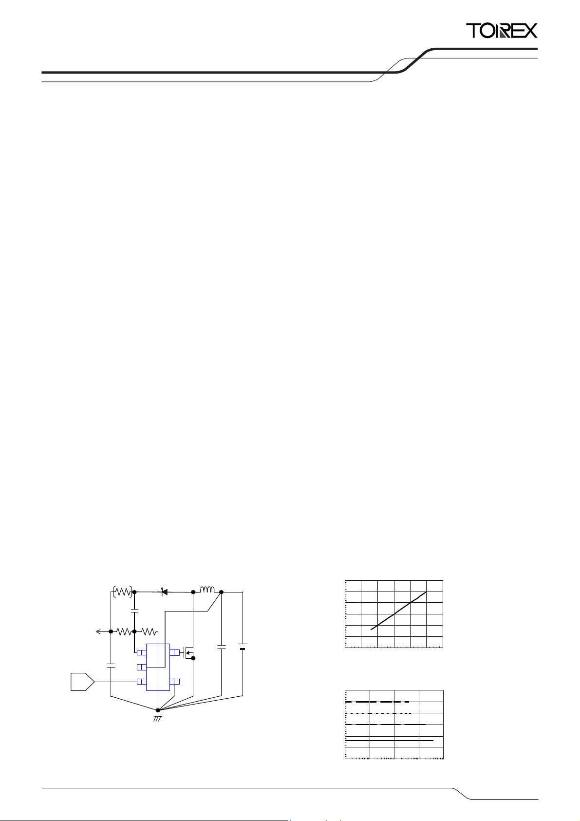
TYPICAL APPLICATION CIRCUIT
V
OUT
= 8V~25V
= 30mA
I
OUT
Ceramic CL :
10
μ
0.8V~2.5V
D/A converter
RSENSE : 10 0m
for Ceramic CL
*
RFB1 :
270k
Ω
CE/Vref
Ω
SD : MA737
CFB : 27p
RFB2 :
30k
Ω
15
2
3
4
L : 10
Nch Pow er
MOS FE
2SK2159
μ
CIN
* RSENSE is of no use in light load (uncontinuous mode)
applications such as a small LCD, even using ceramic
capacitor.
V
= 3.3V
IN
■TYPICAL PERFORMANCE
CHARACTERISTICS
XC9107D003MR
V
30
25
20
(V)
15
OUT
V
10
5
0
0.0 0.5 1.0 1.5 2.0 2.5 3.0
XC9107D003MR
30
25
20
(V)
15
OUT
V
10
5
0
0.1 1 10 100 1000
DD=VIN
☆GreenOperation-Compatible
Vref+0.7V
V
OUT=Vref x (RFB1+RFB2)/RFB2
IN=3.3V, VOUT=20V,
when external components are
used as in the circuits below.)
(XC9107)
: EU RoHS Compliant, Pb Free
Circuit as left
=3.3V, I
=30m A
OUT
Vref (V)
Circuit as left
=3.3V
V
DD=VIN
2.5V
2.0V
1.5V
Vref=0.8V
(mA)
I
OUT
1/11
XC9106/XC9107 Series
■PIN CONFIGURATION
NC
12
FB
■PIN ASSIGNMENT
VDD
SOT-25
(TOP VIEW)
PIN NUMBER
SOT-25 USP-6B
1 6 FB Output Resistor Connection
2 2 VDD Supply Voltage
3 4
4 3 GND Ground
5 1 EXT External Transistor Connection
- 5 NC No Connection
■PRODUCT CLASSIFICATION
●Ordering Information
XC9106D①②③④⑤-⑥
XC9107D①②③④⑤-⑥
DESIGNATOR ITEM SYMBOL DESCRIPTION
GND
45
3
CE/Vref
NAME
FB 6
NC 5
CE/VIEW
PIN
CE/
Serves as Both Chip Enable Pin
Vref
and Reference Voltage Apply Pin.
(*1)
: PWM control
(*1)
: PWM/PFM automatic switching control
FUNCTION
1 EXT
2 VDD
3
*The dissipation pad for the USP-6B package should be
solder-plated in recommended mount pattern and metal
masking so as to enhance mounting strength and heat
release. If the pad needs to be connected to other pins. it
should be connected to the V
DD pin.
①②
③
④⑤-⑥
(*1)
The “-G” suffix indicates that the products are Halogen and Antimony free as well as being fully RoHS compliant.
Reference Voltage
(Apply External)
Oscillation Frequency
Packages
(Oder Unit)
00 Fixed
3 300kHz
1 100kHz
MR
MR-G
DR
DR-G
SOT-25 (3,000/Reel)
SOT-25 (3,000/Reel)
USP-6B (3,000/Reel)
USP-6B (3,000/Reel)
2/11
A
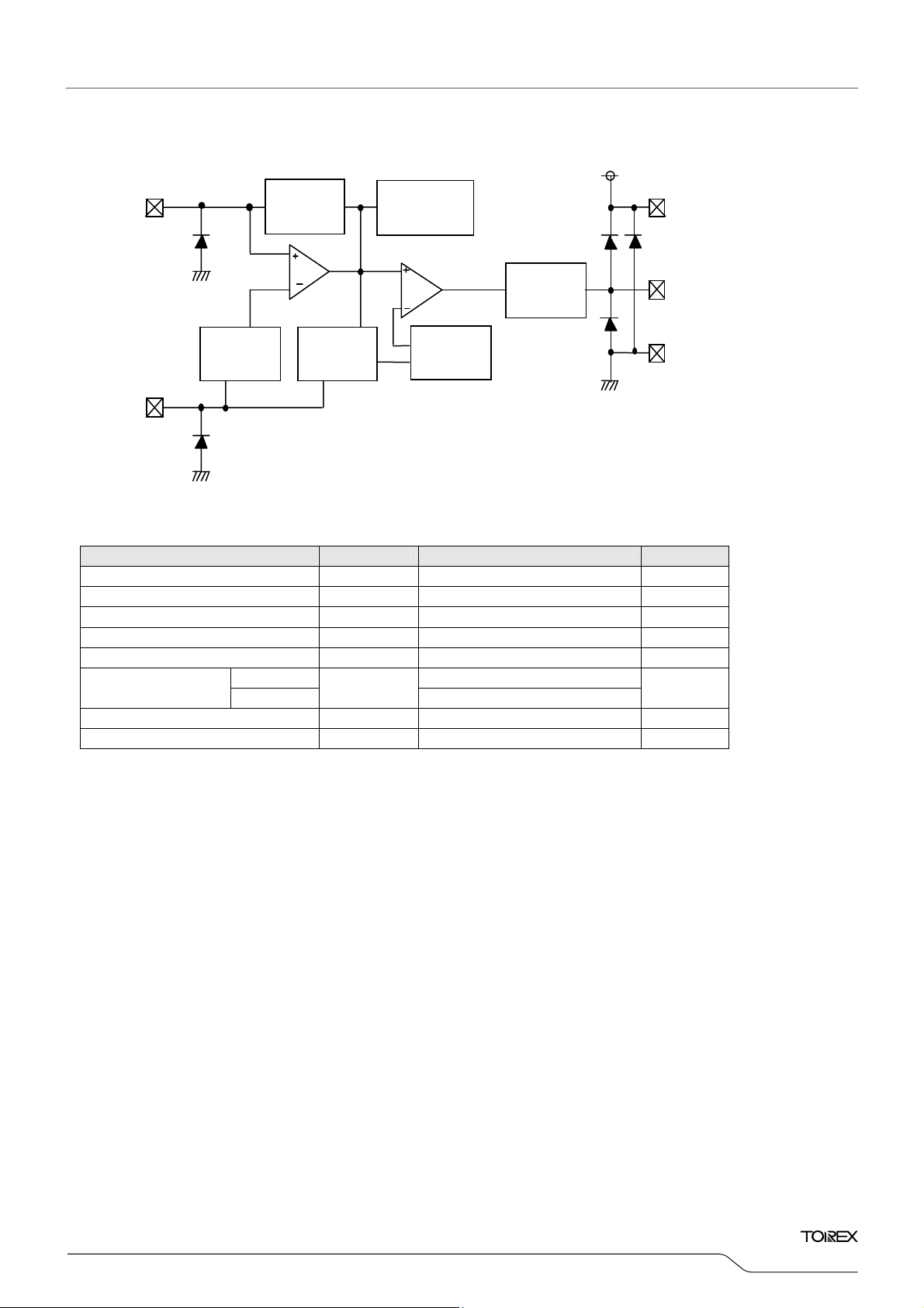
■BLOCK DIAGRAM
FB
Current
Ripple Detect
and FB
Error Amp.
Phase
Compensation
PWM
Comparator
Buffer,
Driver
XC9106/XC9107
Series
VDD
EXT
Vref with
Soft Start,
CE
CE / Vref
■
BSOLUTE MAXIMUM RATINGS
PARAMETER SYMBOL RATINGS UNITS
VDD pin Voltage VDD
FB Pin Voltage VFB
CE / Vref pin Voltage VCE / Vref
EXT pin Voltage VEXT
EXT pin Current IEXT/
Power Dissipation
SOT-25 150
USP-6B
Operating Temperature Range Topr
Storage Temperature Range Tstg
PWM/PFM
Controller
Pd
Ramp Wave
Generator,
OSC
FB, CE : CMOS INPUT
EXT : CMOS OUTPUT
-0.3~12.0
-0.3~12.0
-0.3~12.0
DD+0.3
-0.3~V
±100
100
-40~+85
-55~+125
GND
Ta = 25OC
V
V
V
V
mA
mW
O
C
O
C
3/11
XC9106/XC9107 Series
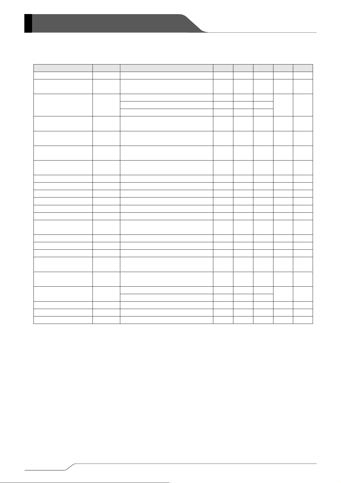
■ELECTRICAL CHARACTERISTICS
XC9106D001MR, XC9107D001MR
(FOSC=100kHz)
PARAMETER SYMBOL CONDITIONS MIN. TYP. MAX.
Output Voltage VOUT Vref = 0.9V 8.820 9.000 9.180 V
Reference
Voltage Range
Vref 0.8 - 2.5 V -
Vref = 0.8V 0.784 0.800 0.816
FB Control Voltage VFB
Vref = 0.9V 0.882 0.900 0.918
Vref = 2.5V 2.450 2.500 2.550
Supply Voltage Range
(*1)
V
DD
Operation Start Voltage VST1
Oscillation
Start Voltage (*1)
V
ST2
Operation Hold Voltage VHLD
CE/Vref=0.9V, V oltage applied, FB=0V
DD as shown right and
V
(Vref applied voltage+0.7V)
Recommended Circuit using
2SD1628, I
OUT=1.0mA
No external connections,
Recommended circuit using
2SD1628, I
OUT=1.0mA
1.8 - 10.0 V -
- - 0.9 V
- - 0.8 V
- - 0.7 V
Supply Current 1 IDD1 Same as VST2, VDD=3.300V - 29 41
Supply Current 2 IDD2 Same as IDD1, FB=1.2V - 14 19
Stand-by Current ISTB Same as IDD1, CE/Vref=0V - - 1.0
Oscillation Frequency FOSC Same as IDD1 85 100 115 kHz
Maximum Duty Ratio MAXDTY Same as IDD1 75 81 87 %
PFM Duty Ratio PFMDTY No Load (XC9106 series) 20 28 36 %
Efficiency EFFI
Recommended circuit using
XP161A1355
- 85 - %
Soft-start Time TSS Vref=0.9V 5.0 10.0 20.0 mS
CE “High” Voltage VCEH Same as IDD1 0.65 - - V
CE “Low” Voltage VCEL Same as IDD1 - - 0.20 V
EXT “High”
ON Resistance
EXT “Low”
ON Resistance
CE “High” Current ICEH
REXTH Same as IDD1, VEXT=VOUT-0.4V - 24 36
REXTL Same as IDD1, VEXT=0.4V - 16 24
Same as IDD2, CE=0.8V -1.0 - 0.0
Same as I
DD2, CE=2.5V 0.0 - 2.5
CE “Low” Current ICEL Same as IDD2, CE=0V - - -0.1
FB “High” Current IFBH Same as IDD2, FB=VDD - - 0.1
FB “Low” Current IFBL Same as IDD2, FB=1.0V - - -0.1
Test Conditions: Unless otherwise stated, CL: Ceramic, recommended MOSFET should be connected.
V
V
NOTE:
*1: Although the IC starts step-up operations from a V
V
DD ≧ 1.8V and (Vref applied voltage+0.7V). Therefore, a VDD of more than 1.8V and (Vref applied voltage+0.7V) is
recommended when V
DD= 3.3V → Vref= 0.09V, RFB1,2×10
IN= 3.3V → IOUT= 50mA
DD of 0.8V, the output voltage and oscillation frequency are stabilized at
DD is supplied from VIN or other power sources.
Ta=25
UNITS CIRCUIT
V
μA
μA
μA
Ω
Ω
μA
μA
μA
μA
①
④
③
④
③
④
④
⑤
④
④
①
①
①
⑤
⑤
④
④
⑤
⑤
⑤
⑤
O
C
4/11

XC9106/XC9107
■ELECTRICAL CHARACTERISTICS (Continued)
XC9106D003MR, XC9107D003MR
PARAMETER SYMBOL CONDITIONS MIN. TYP. MAX. UNITS CIRCUIT
Output Voltage VOUT Vref = 0.9V 8.820 9.000 9.180 V ①
Reference
Voltage Range
Vref 0.8 - 2.5 V
Vref = 0.8V 0.784 0.800 0.816
FB Control Voltage VFB
Vref = 0.9V 0.882 0.900 0.918
Vref = 2.5V 2.450 2.500 2.500
Supply Voltage Range
(*1)
DD
V
Operation Start Voltage VST1
Oscillation
Start Voltage (*1)
V
ST2
Operation Hold Voltage VHLD
Recommended circuit using 2SD1628,
CE/Vref=0.9V, Voltage applied, FB=0V
Recommended circuit using 2SD1628,
DD as shown right and
V
(Vref applied voltage+0.7V)
OUT=1.0mA
I
No external connections
OUT=1.0mA
I
Supply Current 1 IDD1 Same as VST2, VDD=3.3V - 62 88 μA ④
Supply Current 2 IDD2 Same as IDD1, FB=1.2V - 16 22 μA ④
Stand-by Current ISTB Same as IDD1, CE/Vref=0V - - 1.0 μA ⑤
Oscillation Frequency FOSC Same as IDD1 255 300 345 kHz ④
Maximum Duty Ratio MAXDTY Same as IDD1 75 81 87 % ④
PFM Duty Ratio PFMDTY No Load (XC9106 series) 24 32 40 % ①
Efficiency EFFI
Recommended circuit using
XP161A1355
Soft-start Time TSS Vref=0.9V 5.0 10.0 20.0 mS ①
CE “High” Voltage VCEH Same as IDD1 0.65 - - V ⑤
CE “Low” Voltage VCEL Same as IDD1 - - 0.20 V ⑤
EXT “High”
ON Resistance
EXT “Low”
ON Resistance
CE “High” Current ICEH
EXTH Same as IDD1, VEXT=VOUT-0.4V - 24 36 Ω
R
EXTL Same as IDD1, VEXT=0.4V - 16 24 Ω
R
Same as IDD2, CE=0.8V -1.0 - 0.0
Same as I
CE “Low” Current ICEL Same as IDD2, CE=0V - - -0.1 μA ⑤
FB “High” Current IFBH Same as IDD2, FB=VDD - - 0.1 μA ⑤
FB “Low” Current IFBL Same as IDD2, FB=1.0V - - -0.1 μA ⑤
Test Conditions: Unless otherwise stated, CL: Ceramic, recommended MOSFET should be connected.
V
V
NOTE :
■TYPICAL APPLICATION CIRCUIT
*1: Although the IC starts step-up operations from a V
V
DD ≧ 1.8V and (Vref applied voltage+0.7V). Therefore, a VDD of more than 1.8V and (Vref applied voltage+0.7V) is
recommended when V
DD= 3.3V → Vref= 0.09V, RFB1,2 × 10
IN= 3.3V → IOUT= 50mA
DD of 0.8V, the output voltage and oscillation frequency are stabilized at
DD is supplied from VIN or other power sources.
(FOSC=300kHz)
1.8 - 10.0 V
- - 0.9 V
- - 0.8 V ④
- - 0.7 V
- 85 - %
DD2, CE=2.5V 0.0 - 2.5
Series
Ta=25
-
V ④
-
③
③
①
④
④
μA ⑤
O
C
NchPower
MOSFET
When obtaining VDD from a source other than VOUT, please insert a capacitor CDD between the
V
DD pin and the GND pin in order to provide stable operations.
Please wire C
sufficiently. When using a capacitor other than ceramic or low ESR at CL, please take away
R
SENSE and short.
L & CIN between the VOUT/VDD pin and the GND pin. Strengthen the wiring
Rb
Cb
Insert Rb and CB when using a
bipolar NPN Transistor.
5/11

XC9106/XC9107 Series
■OPERATIONAL EXPLANATION
The XC9106 / 07 series are reference voltage (Vref) apply external step-up DC/DC cont roller ICs. Output voltage will be set
with external resistors (R
suited to software applications that need to vary voltage such as LCD power supply for PDA.
<Error Amp.>
Error amplifier is designed to monitor the output voltage, comparing the feedback voltage (FB) with the reference voltage
Vref. In response to feedback of a voltage lower than the reference voltage Vref, the output voltage of the error amp.
decreases.
<OSC Generator>
This circuit generates the internal reference clock.
<Ramp Wave Generator>
The ramp wave generator generates a saw-tooth waveform based on outputs from the OSC generator.
<PWM Comparator>
The PWM comparator compares outputs from the error amp. and saw-tooth waveform. When the voltage from the Error
amp's output is low, the external switch will be set to ON.
<PWM / PFM Controller>
This circuit generates PFM pulses.
The PWM/PFM automatic switching mode switches between PWM and PFM automatically depending on the load.
PWM/PFM control turns into PFM control when threshold voltage becomes lower than voltage of error amps. Noise is easily
reduced with PWM control since the switching frequency is fixed. Because of the function, control suited to the applicat ion
can easily be selected. The series suitable for noise sensitive portable audio equipment as PWM control can suppress noise
during operation and PWM/PFM switching control can reduce consumption current during light loads in stand-by.
<Vref 1 with Soft Start>
The reference voltage of the XC9106/9107 series is adjusted and fixed by external applied voltage. (For output voltage
settings, please refer to the output voltage setting.)
To protect against inrush current, when the power is switched on, and also to protect against voltage overshoot, soft-start time
is set internally to 10ms. It should be noted, however, that this circuit does not protect the load capacitor (C
current. With the Vref voltage limited, and depending upon the input to error amp, the operation maintains a balance between
the two inputs of error amps and controls the EXT pin's ON time so that it doesn't increase more than is necessary.
The XC9106/9107 series alters soft start times by the setting value of reference voltage in order to protect against vol tage
overshoot and also to protect against inrush current. Please determine soft start time by the formula equation.
T
SS = 8.65
×
[Example Computation]
Vref = 0.9V, T
<Enable Function>
This function controls the operation and shutdown of the IC. When the voltage of the CE pin drops to 0.2V or less, disable
mode will be entered, the IC's operations will stop and the EXT pin will be kept at a low level (the external N-ch MOSFET will
be OFF). When the IC is in a state of chip disable, current consumption will be no more than 1.0μA.
When the CE pin's voltage rises to 0.65V or more, enable mode will be entered and operations will recommence. The CE pin
also doubles with reference voltage in the XC9106/9107 series, an d the range of referenc e voltage can be varied externall y
from 0.8V to 2.5V.
FB1 and RFB2) and Vref value. The series make it easy to control output voltage externally and are
L) from inrush
Vref + 2.21
SS = 8.65
×
0.9 + 2.21 = 10.0 ms
30
25
20
15
10
5
Soft Start Time : TSS (ms)
0
0.0 0.5 1.0 1.5 2.0 2.5 3.0
XC9106 / X C9107D xxx MR
Refer ence Voltage V r ef (V)
6/11

XC9106/XC9107
■OPERATIONAL EXPLANATION (Continued)
<Output Voltage Setting>
Output voltage can be set by adding external split resistors. Output voltage is determined by the following equation, based on
the values of R
the series can be varied externally from 0.8V to 2.5V.
The value of CFB1, speed-up capacitor for phase compensation, should result in fzfb = 1/(2π×C
30kHz. Adjustments are required depending on the application, value of inductance (L), and value of load capacity (CL).
fzfb = 30kHz (L=10μH) R
fzfb = 20kHz (L=22μH) C
fzfb = 10kHz (L=47μH) 27pF (fzfb = 20kHz, L = 22μH)
56pF (fzfb = 10kHz, L = 47μH)
<The Use of Ceramic Capacitor CL>
The circuit of the XC9106/9107 series is organized by a specialized circuit, which reenacts negative feedback of both voltage
and current. Also by insertion of approximately 100mΩ of a low and inexpensive sense resistor as current sense, a hig h
degree of stability is possible even using a ceramic capacitor, a condition, which used to be difficult to achieve. Compared to a
tantalum condenser, because the series can be operated in a very small capacity, it is suited to use of the ceramic capacitor,
which is cheap and small.
■RECOMMENDED EXTERNAL COMPONENTS
Tr: *When a MOSFET is used: *When a NPN Tr. is used :
2SK2159 (N-ch Power MOSFET, NEC) 2SD1628 (SANYO)
Note* : With direct voltages over 4.5V, use the Rb : 500Ω (adjust with Tr's HFE or load)
XP161A11A1PR. Cb : 2200pF (ceramic type)
Cb
SD: MA2Q737 (Schottky Diode type, MATSUSHITA)
L, CL : Adjust as below according to the condition and peripheral components
When Ceramic capacitor is used:
L : 22μH (CDRH5D28, SUMIDA, FOSC = 100kHz)
10μH (CDRH5D28, SUMIDA, FOSC = 300kHz)
C
Use the formula below when step-up ratio and output current is large.
C
R
50mΩ (FOSC = 100kHz)
When Tantalum capacitor is used:
L: 22μH (CDRH5D28, SUMIDA, FOSC = 300kHz)
47μH (CDRH5D28, SUMIDA, FOSC = 100kHz)
Except when I
CL: 16V, 47μF (Tantalum type 16MCE476MD2, NIPPONCHEMI)
Use the formula below when step-up ratio and output current is large.
C
R
When AL Electrolytic capacitor is used:
L: 22μH (CDRH5D28, SUMIDA, FOSC = 300kHz)
47μH (CDRH5D28, SUMIDA, FOSC = 100kHz)
Except when I
C
Strengthen appropriately when step-up ratio and output current is large.
R
C
FB1 and RFB2. The sum of RFB1 and RFB2 should normally be 2MΩ or less. The range of reference voltage of
VOUT = Vref applied voltage×(RFB1 + RFB2) / RFB2
FB×RFB1) equal to 5 to
FB1 : 270kΩ RFB2 : 30kΩ
FB : 20pF (fzfb = 30kHz, L = 10μH)
≦
1 / (2π×Rb×FOSC×0.7)
L : 10V, 10μF (Ceramic capacitor, LMK325BJ106ML, TAIYOYUDEN)
L = (CL standard value)
SENSE : 100mΩ (FOSC = 300kHz)
×
(IOUT(mA) / 300mA×VOUT / VIN)
OUT(mA) / 100mA
L = (CL standard value)
SENSE: Not required, but short out the wire.
OUT(mA) / 100mA
L: 16V, 100μF (AL electrolytic type)+10V, 2.2μF (ceramic type)
SENSE: Not required, but short out the wire.
FB: Set up so that fzfb = 100kHz.
×
VOUT / VIN>2 → 22μH
×
(IOUT(mA) / 300mA×VOUT / VIN)
×
VOUT / VIN>2 → 22μH
Series
7/11

XC9106/XC9107 Series
■TEST CIRCUITS
Circuit ① Circuit ④
A
V
IN
L
C
IN
OSC
Tr
Circuit ② Circuit ⑤
A
V
IN
L
CB
Tr
IN
C
RB
Circuit ③
A
V
IN
L
IN
C
CB
Tr
RB
8/11
EXT
CE
OSC
OSC
SD
GND
EXT
CE
EXT
CE
V
DD
FB
SD
GND
SD
GND
V
V
DD
FB
R
CFB
DD
FB
SENSE
C
C
FB
FB
R
R
R
SENSE
R
SENSE
FB1
FB2
A
RFB1
RFB2
CL
RFB1
RFB2
V
OUT
A
CL
CL
V
RL
A
V
RL
A
V
RL
OSC
EXT
CE
EXT
C
CE
E
RP
GND
GND
CP
V
DD
DD
A
A
FB
V
DD
FB
C
AA

■PACKAGING INFORMAT ION
●SOT-25 ●USP-6B
Unit : mm
XC9106/XC9107
Series
Unit : mm
●USP-6B Reference Pattern Layout
●USP-6B Reference Metal Mask Design
9/11

(
XC9106/XC9107 Series
■MARKING RULE
●SOT-25
●USP-6B
54
① ② ③ ④
123
SOT-25
TOP VIEW)
USP-6B
(TOP VIEW)
①② represents product series
③ represents oscillation frequency
MARK OSCILLATION FREQUENCY PRODUCT SERIES
④ represents production lot number
0 to 9,A to Z reverse character 0 to 9,A to Z repeated (G, I, J, O, Q, W excluded)
①② represents product series
③④ represents FB voltage
⑤ represents oscillation frequency
MARK OSCILLATION FREQUENCY PRODUCT SERIES
⑥ represents production lot number
0 to 9,A to Z repeated (G, I, J, O, Q, W excluded).
Note: No character inversion used.
MARK
① ②
6
D
7 D
PRODUCT SERIES
XC9106D00xMx
XC9107D00xMx
1 100kHz XC9106/07D001Mx
3 300kHz XC9106/07D003Mx
MARK
① ②
U
D
PRODUCT SERIES
XC9106D00xDx
L D XC9107D00xDx
MARK
③ ④
0
0
PRODUCT SERIES
XC9106D00xDx
0 0 XC9107D00xDx
1 100kHz XC9106/07D001Dx
3 300kHz XC9106/07D003Dx
10/11

XC9106/XC9107
Series
1. The products and product specifications containe d herein are subject to change without
notice to improve performance characteristics. Consult us, or our representatives
before use, to confirm that the information in this datasheet is up to date.
2. We assume no responsibility for any infringement of patents, patent rights, or other
rights arising from the use of any information and circuitry in this datasheet.
3. Please ensure suitable shipping controls (including fail-safe designs and aging
protection) are in force for equipment employing products listed in this datasheet.
4. The products in this datasheet are not developed, designed, or approved for use with
such equipment whose failure of malfunction can be reasonably expected to directly
endanger the life of, or cause significant injury to, the user.
(e.g. Atomic energy; aerospace; transport; combustion and associated safety
equipment thereof.)
5. Please use the products listed in this datasheet within the specified ranges.
Should you wish to use the products under conditions exceeding the specifications,
please consult us or our representatives.
6. We assume no responsibility for damage or loss due to abnormal use.
7. All rights reserved. No part of this datasheet may be copied or reproduced without the
prior permission of TOREX SEMICONDUCTOR LTD.
11/11
 Loading...