


)
XC8101 Series
ETR2501-007
High Side Load Switch with Low Supply Current
■ GENERAL DESCRIPTION
The XC8101 series is a low supply current load switch IC with ON/OFF control and output current protection which integrates
P-channel MOSFET. The XC8101 is suited for power distribution switch. With connecting to the output pin of step-down DC/DC
converters, the CE pin controls ON/OFF for each distribution switch to deliver power per requirements and maximize total
power efficiency. As result, the XC8101 helps extend battery life and product operation time. The XC8101 is available in an
ultra small package USP-4 and does not require any external capacitors so that it can provide small power unit design and
board space saving. When low signal is input to the CE pin, the XC8101 enters stand-by mode. Even where a load capacitor is
connected to the output pin during in the stand-by mode, the internal switch between the V
the electric charge in the load capacitor to be discharged. Because of this discharge function, the V
quickly to V
The XC8101 contains an over current protection with foldback current circuitry which operates as over current protection and
short circuit protection for the output pin.
■APPLICATIONS
● Mobile phones, Smart phones
● Digital still cameras, Digital video cameras
● Portable games
● Portable equipment
■TYPICAL APPLICATION CIRCUIT
level.
SS
■FEATURES
On Resistance : 0.75Ω@ VIN=2.9V (TYP.)
: 1.15Ω@ VIN=1.8V (TYP.)
Output Current : 200mA
Input Voltage Range : 1.8V~6.0V
Power Consumption : 3.0μA@ V
Stand-by Current : 0.1μA
Protection Circuit : Current limit, 300mA (TYP.)
: Short-circuit Protection,
ON/OFF Function : High Active Enable
High-Speed Discharge Function
Operating Temperature Range : -40℃~85℃
Packages
Environmentally Friendly
■ TYPICAL PERFORMANCE
CHARACTERISTICS
●Supply Current vs. Input Voltage
and VSS of the XC8101 enables
OUT
OUT pin voltage falls
<Current Limit =300mA (TYP.)>
=1.8V
IN
Short current= 30mA (TYP.)
: USP-4, SSOT-24, SOT-25
: EU RoHS Compliant, Pb Free
XC8101AA01
VIN=CE
6.0
5.0
4.0
3.0
2.0
Supply Current: IDD (μA
1.0
0.0
0.0 0.5 1.0 1.5 2.0 2.5 3.0 3.5 4.0 4 .5 5. 0 5. 5 6. 0
Input Voltage: VIN (V)
CIN=Non e, CL =No ne
Ta=8 5
℃
25
℃
-40
℃
1/37

XC8101 Series
■PIN CONFIGURATION
*The heat dissipation pad of the USP-4
package is recommended to solder as
shown in the recommended mount pattern
and metal mask pattern for mounting
strength. The heat dissipation pad should
be electrically opened or connected to the
V
(No. 2) pin.
SS
■PIN ASSIGNMENT
■PRODUCT CLASSIFICATION
■FUNCTION CHART
USP-4
(BOTTOM VIEW)
PIN NUMBER
USP-4 SOT-25 SSOT-24
4 1 4 VIN Power Input
1 5 3 V
2 2 2 VSS Ground
3 3 1 CE ON/OFF Control
- 4 - NC No Connection
●Ordering Information
XC8101①②③④⑤⑥-⑦
(*1)
DESIGNATOR ITEM SYMBOL DESCRIPTION
①
② C
③④
⑤⑥-⑦
(*1)
The “-G” suffix indicates that the products are Halogen and Antimony free as well as being fully RoHS compliant.
(*1)
CE pin logic
Discharge Function A
L
Internal Standard
Packages
(Order Unit)
SERIES CE
XC8101AA01
High ON
Low OFF
SOT-25
(TOP VIEW)
PIN NAME FUNCTIONS
Number
IC OPERATIONAL STATUS
SSOT-24
(TOP VIEW)
Output
OUT
A High active enable
Output capacitor (C
function integrated
01 Fixed
GR-G
MR-G
NR-G
USP-4 (3,000/Reel)
SOT-25 (3,000/Reel)
SSOT-24 (3,000/Reel)
ON/OFF
) auto-discharge
L
2/37

■BLOCK DIAGRAM
●XC8101AA Series
XC8101
Series
* Diodes inside the circuit are an ESD protection diode and a parasitic diode.
■ABSOLUTE MAXIMUM RATINGS
PAR AMETER SYMBOL RATINGS UNITS
Input Voltage
Output Current
Output Voltage
CE Input Voltage
USP-4
Power Dissipation
Operating Temperature Range
Storage Temperature Range
* Please make sure that I
SOT-25 250
SSOT-24
is less than Pd/(VIN-V
OUT
OUT
).
Ta =2 5℃
VIN
I
450 * mA
OUT
V
OUT
VCE
-0.3~+6.5
V
SS
-0.3~VIN
V
SS
-0.3~+6.5
V
SS
V
V
V
120
Pd
mW
150
Topr
Ts tg
-40~+85
-55~+125
o
C
o
C
3/37

XC8101 Series
■ELECTRICAL CHARACTERISTICS
●XC8101AA Series
PAR AMETER SYMBOL CONDITIONS MIN. TYP. MAX. UNITS CIRCUIT
Input Voltage VIN 1.8 - 6.0 V -
VIN=6.0V, VCE=VIN - 0.55 0.90
On Resistance
(SSOT-24 / USP-4)
On Resistance
(SOT-25)
Supply Current IDD
Stand-by Current I
Switch Leakage Current I
Current Limit I
Short Circuit Current I
CE High Level Voltage V
CE Low Level Voltage V
CE High Level Current I
CE Low Level Current I
CL Auto-Discharge
Resistance
Turn On Time
Turn Off Time
NOTE:
*1: Time to reach 90% of V
*2: Time to fall to 10% of V
(*1)
t
(*2)
t
after VCE entering the V
OUT
after VCE entering the V
OUT
R
ON
R
ON
STBY
LEAK
LIM
SHORT
CEH
CEL
CEH
CEL
R
DCHG
DLY(ON)
DLY(OFF)
VIN=4.0V, VCE=VIN - 0.65 1.00
VIN=2.9V, VCE=VIN - 0.75 1.10
V
=1.8V, VCE=VIN - 1.15 1.50
IN
VIN=6.0V, VCE=VIN - 0.65 1.00
VIN=4.0V, VCE=VIN - 0.75 1.10
VIN=2.9V, VCE=VIN - 0.85 1.20
V
=1.8V, VCE=VIN - 1.25 1.60
IN
VIN=6.0V, VCE=VIN, V
VIN=4.0V, VCE=VIN, V
VIN=2.9V, VCE=VIN, V
V
=1.8V, VCE=VIN, V
IN
VIN=6.0V, VCE=VSS, V
VIN=6.0V, VCE=V
VCE=V
VCE=VIN, V
IN, VOUT
= V
=0V - 30 - mA ①
OUT
1.2 - 6.0 V ③
- - 0.3 V ③
VCE=VIN -0.1 - 0.1 μA ③
VCE=VSS -0.1 - 0.1 μA ③
VIN=4.0V, V
V
=4.0V, VCE=0.3V→1.2V,
IN
R
L=80Ω, without C
V
=4.0V, VCE=1.2V→0.3V,
IN
R
L=80Ω, without C
threshold.
CEH
threshold.
CEL
=4.0V, VCE=VSS 650 900 1100 Ω ④
OUT
Ω ①
Ω ①
=OPEN - 2.7 8.2
OUT
=OPEN - 2.3 7.3
OUT
=OPEN - 2.2 6.9
OUT
=OPEN - 2.0 6.2
OUT
=OPEN - 0.01 0.10 μA ②
OUT
OUT=VSS
- 0.01 0.10 μA ②
- 1.0V 200 300 - mA ①
IN
IN,CL
IN,CL
- 6 13 μs ⑤
- 2.0 4.0 μs ⑤
μA ②
Ta =2 5 ℃
4/37

■TEST CIRCUITS
Circuit ①
Circuit ②
XC8101
Series
Circuit ③
5/37

XC8101 Series
■TEST CIRCUITS (Continued)
Circuit ④
Circuit ⑤
The measurement point of wave form
The measurement point of wave form
6/37

XC8101
Series
■OPERATIONAL EXPLANATION
<CE Pin>
The XC8101 enables an output P-channel MOSFET switch and the IC internal circuitry to turn off by the signal to the CE pin. In
the shutdown mode, the V
The output voltage becomes unstable when the CE pin is opened. If the input voltage to the CE pin is within the specified
threshold voltages, the logic is fixed and the XC8101 will operate normally. However, supply current may increase as a result
of the shoot-through current of internal circuitry when the medium level voltage is input to the CE pin.
<Input Capacitor>
The XC8101 works well without an output capacitor (C
to the output side of the IC, input voltage ringing may occur when the IC is turned on. In order to reduce the ringing, an input
capacitor with the value of 1μF or more is requested to attach between V
placed as close as the IC.
<CL Auto-Discharge Function>
The XC8101A contains a C
XC8101A quickly discharge the electric charge in the output capacitor (C
whole IC circuit. . The C
capacitor (C
defined as (τ = C x R
V = V
) is determined by a CL auto-discharge resistor value (R
L
DCHG
OUT x e
V: Output voltage after starting discharge
V
OUT: Output voltage
t: Discharge time
τ: Output discharge resistor value Rdischg×Output capacitor (CL) value C
<Current Limiter, Short-Circuit Protection>
The XC8101 series contains a constant current limiter and foldback current circuitry. The constant current limiter operates to
limit output current and the foldback current circuitry operates as short circuit protection for the output pin.
When the load current reaches the limit current, the constant current limiter operates and the output voltage drops. The output
voltage further, then the foldback current circuitry operates to decrease the output current. When the output pin is short-circuited
to the ground, the output current drops and maintains a flow about 30mA.
pin will be pulled down to the VSS by the CL auto-discharge function.
OUT
L). However, an output capacitor such as a bypass capacitor is tied up
pin and VSS pin. The capacitor should be tied and
IN
auto-discharge resistor and an N-channel transistor between the VOUT pin and the VSS pin. The
L
) when a low signal to the CE pin is input to turn off a
L
auto-discharge resistance is set at 900Ω (V
L
). Output voltage after starting discharge can be calculated by the following formula.
–t/
τ
, or t=τIn (VOUT / V)
=4.0V TYP. @ VIN=4.0). Discharge time of the output
OUT
) and an output capacitor value. Time constant τ is
DCHG
■NOTES ON USE
1. Please use this IC within the stated absolute maximum ratings. Operation beyond these limits may cause degrading or
permanent damage to the device.
2. The X8101 goes into an undefined operation when the CE pin is left open. The CE pin shall be tied to low or high level.
3. V
pin voltage should not be applied beyond the VIN pin voltage. The IC may get damage due to the reverse current
OUT
toward the VIN pin.
7/37

E
E
E
)
)
XC8101 Series
■TYPICAL PERFORMANCE CHARACTERISTICS
(1) ON Resistance vs. Input Voltage
XC8101AA01N / XC8101AA01G
2.0
1.6
1.2
0.8
ON R esistance: RO N (Ω)
0.4
0.0
1.5 2.0 2.5 3.0 3.5 4.0 4.5 5.0 5.5 6.0
Input Voltage: VIN (V)
(2) ON Resistance vs. Ambient Temperature
XC8101AA01N / XC8101AA 01G
2.0
1.6
1.2
0.8
ON Resistance: RO N (Ω)
0.4
VIN=1.8V
VIN=C
IOUT=100mA
CIN=None , CL=None
Ta=8 5
℃
25
℃
-40
℃
VIN=C
IOUT=100mA
CIN=Non e , CL= Non e
2.9V
4.0V
6.0V
XC8101AA01M
2.0
1.6
1.2
0.8
ON Resistance: RON (Ω)
0.4
0.0
1.5 2.0 2.5 3.0 3.5 4.0 4.5 5.0 5.5 6.0
Input Voltage: VIN (V)
XC8101AA01M
2.0
1.6
1.2
0.8
ON Resistance: RON (Ω)
0.4
VIN=1.8V
VIN=C
IOUT=100mA
CIN=None , CL=None
Ta=8 5
V IN=CE
IOU T=1 0 0mA
CIN=Non e , CL=No ne
2.9V
6.0V
25
-40
℃
℃
℃
4.0V
0.0
-50 -25 0 25 50 75 100
Ambient Temperature: Ta (℃)
0.0
-50-250 255075100
Ambient Temperature: Ta (℃)
(3) Supply Current vs. Input Voltage
XC8101AA 01
V IN=CE
6.0
5.0
4.0
3.0
2.0
Supply Current: IDD (μA
1.0
0.0
0.00.51.01.52.02.53.03.54.04.55.05.56.0
Input Voltage: VIN (V)
CIN=None, CL=None
Ta=8 5
25
-40
℃
℃
℃
(4) Supply Current vs. Ambient Temperature
XC8101AA01
V IN=CE
6.0
5.0
4.0
3.0
2.0
Supply Current: IDD (uA
1.0
0.0
-50-250 255075100
Ambient Temperature: Ta (℃)
CIN=Non e , CL =No ne
VIN=6.0V
4.0V
2.9V
1.8V
8/37

■TYPICAL PERFORMANCE CHARACTERISTICS (Continued)
(5) Output Voltage vs. Output Current
XC8101
Series
XC8101AA01N / XC8101AA 01G
V IN=CE=1. 8V
5.0
4.0
3.0
2.0
1.0
Output Voltage: VOUT (V)
0.0
0 50 100 150 200 250 300 350 400 450
Output Current: IOUT (mA)
CIN=None , CL=Non e
Ta=8 5
25
-40
5.0
℃
℃
℃
4.0
3.0
2.0
1.0
Output Voltage: VOUT (V)
0.0
0 50 100 150 200 250 300 350 400 450
XC8101AA01N / XC8101AA 01G
V IN=CE=2.9 V
CIN=None , CL= Non e
Output Current: IOUT (mA)
Ta=8 5
25
-40
℃
℃
℃
XC8101AA01N / XC8101AA 01G
V IN=CE=4 .0V
5.0
4.0
3.0
2.0
CIN=Non e, CL =No ne
Ta=8 5
25
-40
℃
℃
℃
10.0
8.0
6.0
4.0
XC8101AA01N / XC8101AA01G
V IN=CE=6.0 V
CIN=None , CL =Non e
Ta=8 5
25
-40
℃
℃
℃
1.0
Output Voltage: VOUT (V)
0.0
0 50 100 150 200 250 300 350 400 450
Output Curre nt: IOUT (mA)
2.0
Output Voltage: VOUT (V)
0.0
0 50 100 150 200 250 300 350 400 450
Output Current: IOUT (A )
XC8101AA01M
VIN=CE=1.8V
5.0
4.0
3.0
2.0
1.0
Output Voltage: VOUT ( V)
0.0
0 50 100 150 200 250 300 350 400 450
Output Current: IOUT (mA)
CIN=None , CL=Non e
Ta=85
25
-40
5.0
℃
℃
℃
4.0
3.0
2.0
1.0
Output Voltage: VOUT (V)
0.0
0 50 100 150 200 250 300 350 400 450
XC8101AA 01M
Output Current: IOUT (mA)
V IN=CE=2.9 V
CIN=Non e, CL= Non e
Ta=85
25
-40
℃
℃
℃
9/37

XC8101 Series
■TYPICAL PERFORMANCE CHARACTERISTICS (Continued)
(5) Output Voltage vs. Output Current (Continued)
XC8101AA 01M
VIN=CE=4.0V
5.0
4.0
3.0
2.0
1.0
Output Voltage: VOUT (V)
0.0
0 50 100 150 200 250 300 350 400 450
Output Current: IOUT (mA)
CIN=Non e, CL= Non e
Ta=8 5
25
-40
℃
℃
℃
(6) CE Threshold Voltage vs. Ambient Temperature
XC8101AA01
VIN=6.0V
1.00
0.90
0.80
0.70
0.60
0.50
0.40
CE Thres hold Voltage: VCEH,VCEL (V)
-50 -25 0 25 50 75 100
VCEH
VCEL
Ambient Temper ature: Ta (℃)
CIN=No ne , CL =None
(8) Output Turn-on Time with CE
XC8101AA01M
10.0
8.0
6.0
4.0
2.0
Output Voltage: VOUT (V)
0.0
0 50 100 150 200 250 300 350 400 450
Output Current: IOUT (A )
V IN=CE=6 .0V
CIN=Non e, CL=Non e
Ta=8 5
25
-40
℃
℃
℃
(7) CL Discharge Resistance vs. Ambient Temperature
XC8101AA01
2000
1600
1200
800
400
CL Discharge Res istance: Rdisc hg (Ω)
0
-50-250 255075100
Ambient Temperature: Ta (℃)
VIN=VOUT
CE=V SS
CIN=Non e, CL =No ne
VIN=1.8V
2.9V
4.0V
6.0V
1.5
1.0
0.5
0.0
-0.5
-1.0
CE Input Voltage: VCE (V)
-1.5
-2.0
10/37
XC8101AA 01
CE Input Voltage
Output Voltage
Time: 10 μs/div
VIN=1.8V
CE=0. 3V→1.2V
tr=tf=5μs , IOUT=50mA
CIN=Non e , CL= Non e
XC8101AA01
6
5
4
3
2
1
Output Voltage :VO UT ( V)
0
-1
1.5
1.0
0.5
0.0
-0.5
-1.0
CE Input Voltage: VCE (V)
-1.5
-2.0
CE Input Voltage
Time: 4 μs/div
VIN=2.9V
CE=0. 3V→1.2V
tr=tf=5μs , IOUT=50mA
CIN=Non e , CL= Non e
Output Voltage
6
5
4
3
2
1
Output Voltage: VOUT (V)
0
-1

■TYPICAL PERFORMANCE CHARACTERISTICS (Continued)
(8) Output Turn-on Time with CE (Continued)
XC8101
Series
XC8101AA01
1.5
1.0
0.5
0.0
-0.5
-1.0
CE Input Voltage: VCE (V)
-1.5
-2.0
CE Input Voltage
Time: 4 μs/div
VIN=4.0V
CE=0. 3V→1.2V
tr=tf =5μs , IOUT=50mA
CIN=No ne , CL =None
Output Voltage
12
10
8
6
4
2
Output Voltage: VOUT (V)
0
-2
1.5
1.0
0.5
0.0
CE Input Voltage
-0.5
-1.0
CE Input Voltage: VCE (V)
-1.5
-2.0
XC8101AA01
Time: 4μs/div
VIN=6.0V
CE=0.3 V→1.2V
tr=tf =5μs , IOUT=50mA
CIN=None , CL=None
Output Voltage
12
10
8
6
4
2
Output Voltage: VOUT (V)
0
-2
XC8101AA 01
1.5
1.0
0.5
0.0
-0.5
-1.0
CE Input Voltage: VCE (V)
-1.5
-2.0
CE Inpu t V olta ge
Time: 1 0μs/div
VIN=1.8V
CE=0. 3V→1.2V
tr=tf =5μs , IOUT=50mA
CIN=Non e , CL= 0. 1μF
Output Voltage
6.0
5.0
4.0
3.0
2.0
1.0
0.0
-1.0
1.5
1.0
0.5
0.0
-0.5
-1.0
CE Input Voltage: VCE ( V)
Output Voltage :VO UT ( V)
-1.5
-2.0
XC8101AA01
CE Input Voltage
Output Voltage
Time: 10 μs/div
VIN=2.9V
CE=0. 3V→1.2V
tr=tf=5μs , IOUT=50mA
CIN=Non e , CL= 0. 1μF
6.0
5.0
4.0
3.0
2.0
1.0
0.0
-1.0
Output Voltage :VO UT (V)
XC8101AA01
1.5
1.0
0.5
0.0
-0.5
-1.0
CE Input Voltage: VCE (V)
-1.5
-2.0
CE Input Voltage
Time: 10 μs/div
VIN=4.0V
CE=0.3 V→1.2V
tr=tf=5μs , IOUT=50mA
CIN=Non e , CL= 0. 1μF
Output Voltage
12.0
10.0
8.0
6.0
4.0
2.0
0.0
-2.0
1.5
1.0
0.5
0.0
-0.5
-1.0
CE Input Voltage: VCE (V)
Output Voltage :VOUT (V)
-1.5
-2.0
XC8101AA01
CE Input Voltage
Output Voltage
Time: 1 0μs/div
VIN=6.0V
CE=0. 3V→1.2V
tr=tf =5μs , IOUT=50mA
CIN=Non e , CL =0 .1μF
12.0
10.0
8.0
6.0
4.0
2.0
0.0
-2.0
Output Voltage :VOUT ( V)
11/37

XC8101 Series
■TYPICAL PERFORMANCE CHARACTERISTICS (Continued)
(8) Output Turn-on Time with CE (Continued)
XC8101AA 01
1.5
1.0
0.5
0.0
-0.5
-1.0
CE Input Voltage: VC E (V)
-1.5
-2.0
CE Inpu t V olta ge
Time: 1 0μs/div
VIN=1.8V
CE=0. 3V→1.2V
tr=tf =5μs , IOUT=50mA
CIN=Non e , CL= 0. 47μF
Output V oltage
6.0
5.0
4.0
3.0
2.0
1.0
0.0
-1.0
1.5
1.0
0.5
0.0
-0.5
-1.0
CE Input Voltage: VCE (V)
Output Voltage :VO UT ( V)
-1.5
-2.0
XC8101AA01
CE Input Voltage
Time: 10 μs/div
VIN=2.9V
CE=0. 3V→1.2V
tr=tf=5μs , IOUT=50mA
CIN=Non e , CL= 0. 47μF
Output Voltage
6.0
5.0
4.0
3.0
2.0
1.0
0.0
-1.0
Output Voltage :VOUT (V)
XC8101AA01
1.5
1.0
0.5
0.0
-0.5
-1.0
CE Input Voltage: VCE (V)
-1.5
-2.0
CE Input Voltage
Time: 1 0μs/div
VIN=4.0V
CE=0.3 V→1.2V
tr=tf=5μs , IOUT=50mA
CIN=Non e , CL= 0. 47μF
Output Voltage
12.0
10.0
8.0
6.0
4.0
2.0
0.0
-2.0
1.5
1.0
0.5
0.0
-0.5
-1.0
CE Input Voltage: VCE (V)
Output Voltage :VOU T (V)
-1.5
-2.0
XC8101AA01
CE Input Voltage
Time: 1 0μs/div
VIN=6.0V
CE=0. 3V→1.2V
tr=tf =5μs , IOUT=50mA
CIN=Non e , CL =0 .4 7μF
Output V oltage
12.0
10.0
8.0
6.0
4.0
2.0
0.0
-2.0
Output Voltage :VOUT ( V)
XC8101AA 01
1.5
1.0
0.5
0.0
-0.5
-1.0
CE Input Voltage: VCE (V)
-1.5
-2.0
CE Inpu t V olta ge
Time: 1 0μs/div
VIN=1.8V
CE=0. 3V→1.2V
tr=tf =5μs , IOUT=50mA
CIN=Non e, CL= 1μF
Output Voltage
6.0
5.0
4.0
3.0
2.0
1.0
0.0
-1.0
1.5
1.0
0.5
0.0
-0.5
-1.0
CE Input Voltage: VCE (V)
Output Voltage :VO UT ( V)
-1.5
-2.0
XC8101AA01
CE Input Voltage
Output Voltage
Time: 10 μs/div
VIN=2.9V
CE=0. 3V→1.2V
tr=tf=5μs , IOUT=50mA
CIN=Non e , CL= 1μF
6.0
5.0
4.0
3.0
2.0
1.0
0.0
-1.0
Output Voltage :VOUT (V)
12/37

■TYPICAL PERFORMANCE CHARACTERISTICS (Continued)
(8) Output Turn-on Time with CE (Continued)
XC8101
Series
XC8101AA01
1.5
1.0
0.5
0.0
-0.5
-1.0
CE Input Voltage: VCE (V)
-1.5
-2.0
CE Input Voltage
Time: 1 0μs/div
VIN=4.0V
CE=0.3 V→1.2V
tr=tf=5μs , IOUT=50mA
CIN=Non e , CL= 1μF
Output Voltage
12.0
10.0
8.0
6.0
4.0
2.0
0.0
-2.0
1.5
1.0
0.5
0.0
-0.5
-1.0
CE Input Voltage: VCE (V)
Output Voltage :VOU T (V)
-1.5
-2.0
XC8101AA01
CE Input Voltage
Output Voltage
Time: 2 0μs/div
VIN=6.0V
CE=0. 3V→1.2V
tr=tf =5μs , IOUT=50mA
CIN=Non e , CL =1μF
12.0
10.0
8.0
6.0
4.0
2.0
0.0
-2.0
Output Voltage :VOUT (V)
XC8101AA 01
1.5
1.0
0.5
0.0
-0.5
-1.0
CE Input Voltage: VCE (V)
-1.5
-2.0
CE Inpu t V olta ge
Time: 1 0μs/div
VIN=1.8V
CE=0. 3V→1.2V
tr=tf =5μs , IOUT=50mA
CIN=0. 1μF , CL=0.1μF
Output Voltage
6.0
5.0
4.0
3.0
2.0
1.0
0.0
-1.0
1.5
1.0
0.5
0.0
-0.5
-1.0
CE Input Voltage: VCE (V)
Output Voltage :VO UT ( V)
-1.5
-2.0
XC8101AA01
CE Input Voltage
Output Voltage
Time: 10 μs/div
VIN=2.9V
CE=0. 3V→1.2V
tr=tf=5μs , IOUT=50mA
CIN=0. 1μF , CL= 0.1μF
6.0
5.0
4.0
3.0
2.0
1.0
0.0
-1.0
Output Voltage :VO UT ( V)
XC8101AA01
1.5
1.0
0.5
0.0
-0.5
-1.0
CE Input Voltage: VCE (V)
-1.5
-2.0
CE Input Voltage
Time: 10 μs/div
VIN=4.0V
CE=0.3 V→1.2V
tr=tf=5μs , IOUT=50mA
CIN=0. 1μF , CL=0.1μF
Output Voltage
12.0
10.0
8.0
6.0
4.0
2.0
0.0
-2.0
1.5
1.0
0.5
0.0
-0.5
-1.0
CE Input Voltage: VCE (V)
Output Voltage :VOUT (V)
-1.5
-2.0
XC8101AA01
CE Input Voltage
Output Voltage
Time: 1 0μs/div
VIN=6.0V
CE=0. 3V→1.2V
tr=tf =5μs , IOUT=50mA
CIN=0. 1μF , CL=0 .1μF
12.0
10.0
8.0
6.0
4.0
2.0
0.0
-2.0
Output Voltage :VOUT ( V)
13/37
XC8101 Series
■TYPICAL PERFORMANCE CHARACTERISTICS (Continued)
(8) Output Turn-on Time with CE (Continued)
XC8101AA 01
1.5
1.0
0.5
0.0
-0.5
-1.0
CE Input Voltage: VCE (V)
-1.5
-2.0
CE Inpu t V olta ge
Time: 1 0μs/div
VIN=1.8V
CE=0. 3V→1.2V
tr=tf =5μs , IOUT=50mA
CIN=0. 1μF , CL=0.47μF
Output Voltage
6.0
5.0
4.0
3.0
2.0
1.0
0.0
-1.0
1.5
1.0
0.5
0.0
-0.5
-1.0
CE Input Voltage: VCE (V)
Output Voltage :VO UT ( V)
-1.5
-2.0
XC8101AA01
CE Input Voltage
Output Voltage
Time: 10 μs/div
VIN=2.9V
CE=0. 3V→1.2V
tr=tf=5μs , IOUT=50mA
CIN=0.1μF , CL= 0.4 7μF
6.0
5.0
4.0
3.0
2.0
1.0
0.0
-1.0
Output Voltage :VOU T (V)
XC8101AA01
1.5
1.0
0.5
0.0
-0.5
-1.0
CE Input Voltage: VCE (V)
-1.5
-2.0
CE Input Voltage
Time: 1 0μs/div
VIN=4.0V
CE=0.3 V→1.2V
tr=tf=5μs , IOUT=50mA
CIN=0.1μF , CL=0.47μF
Output Voltage
12.0
10.0
8.0
6.0
4.0
2.0
0.0
-2.0
1.5
1.0
0.5
0.0
-0.5
-1.0
CE Input Voltage: VCE (V)
Output Voltage :VOU T (V)
-1.5
-2.0
XC8101AA01
CE Input Voltage
Time: 1 0μs/div
VIN=6.0V
CE=0. 3V→1.2V
tr=tf =5μs , IOUT=50mA
CIN=0. 1μF , CL=0 .47μF
Output V oltage
12.0
10.0
8.0
6.0
4.0
2.0
0.0
-2.0
Output Voltage :VOUT ( V)
1.5
1.0
0.5
0.0
-0.5
-1.0
CE Input Voltage: VC E (V)
-1.5
-2.0
14/37
XC8101AA01
CE Inpu t V olta ge
Time: 1 0μs/div
VIN=1.8V
CE=0. 3V→1.2V
tr=tf =5μs , IOUT=50mA
CIN=0. 1μF , CL= 1μF
Output Voltage
6.0
5.0
4.0
3.0
2.0
1.0
0.0
-1.0
XC8101AA01
1.5
1.0
0.5
0.0
-0.5
-1.0
CE Input Voltage: VCE (V)
Output Voltage :VO UT (V)
-1.5
-2.0
CE Input Voltage
Time: 10 μs/div
VIN=2.9V
CE=0. 3V→1.2V
tr=tf=5μs , IOUT=50mA
CIN=0.1μF , CL= 1μF
Output Voltage
6.0
5.0
4.0
3.0
2.0
1.0
0.0
-1.0
Output Voltage :VOU T (V)

■TYPICAL PERFORMANCE CHARACTERISTICS (Continued)
(8) Output Turn-on Time with CE (Continued)
XC8101
Series
XC8101AA01
1.5
1.0
0.5
0.0
-0.5
-1.0
CE Input Voltage: VC E (V)
-1.5
-2.0
CE Input Voltage
Time: 1 0μs/div
VIN=4.0V
CE=0.3 V→1.2V
tr=tf=5μs , IOUT=50mA
CIN=0.1μF , CL=1μF
Output Voltage
12.0
10.0
8.0
6.0
4.0
2.0
0.0
-2.0
1.5
1.0
0.5
0.0
-0.5
-1.0
CE Input Voltage: VCE (V)
Output Voltage :VOUT (V)
-1.5
-2.0
XC8101AA01
CE Input Voltage
Output Voltage
Time: 1 0μs/div
VIN=6.0V
CE=0. 3V→1.2V
tr=tf =5μs , IOUT=50mA
CIN=0. 1μF , CL=1μF
12.0
10.0
8.0
6.0
4.0
2.0
0.0
-2.0
Output Voltage :VOUT (V)
XC8101AA01
1.5
1.0
0.5
0.0
-0.5
-1.0
CE Input Voltage: VCE (V)
-1.5
-2.0
CE Inpu t V olta ge
Time: 1 0μs/div
VIN=1.8V
CE=0. 3V→1.2V
tr=tf =5μs , IOUT=50mA
CIN=0. 22μF , CL=0 .1μF
Output Voltage
6.0
5.0
4.0
3.0
2.0
1.0
0.0
-1.0
1.5
1.0
0.5
0.0
-0.5
-1.0
CE Input Voltage: VCE ( V)
Output Vo ltage :VOUT (V)
-1.5
-2.0
XC8101AA01
CE Input Voltage
Output Voltage
Time: 10 μs/div
VIN=2.9V
CE=0. 3V→1.2V
tr=tf=5μs , IOUT=50mA
CIN=0.2 2μF , CL=0.1μF
6.0
5.0
4.0
3.0
2.0
1.0
0.0
-1.0
Output Voltage :VOU T (V)
XC8101AA01
1.5
1.0
0.5
0.0
-0.5
-1.0
CE Input Voltage: VCE (V)
-1.5
-2.0
CE Input Voltage
Time: 10 μs/div
VIN=4.0V
CE=0.3 V→1.2V
tr=tf=5μs , IOUT=50mA
CIN=0.2 2μF , CL=0.1μF
Output Voltage
12.0
10.0
8.0
6.0
4.0
2.0
0.0
-2.0
1.5
1.0
0.5
0.0
-0.5
-1.0
CE Input Voltage: VCE (V)
Output Voltage :VOUT (V)
-1.5
-2.0
XC8101AA01
CE Input Voltage
Output Voltage
Time: 1 0μs/div
VIN=6.0V
CE=0. 3V→1.2V
tr=tf =5μs , IOUT=50mA
CIN=0. 22μF , CL=0.1μF
12.0
10.0
8.0
6.0
4.0
2.0
0.0
-2.0
Output Voltage :VOUT ( V)
15/37

XC8101 Series
■TYPICAL PERFORMANCE CHARACTERISTICS (Continued)
(8) Output Turn-on Time with CE (Continued)
XC8101AA01
1.5
1.0
0.5
0.0
-0.5
-1.0
CE Input Voltage: VC E (V)
-1.5
-2.0
CE Inpu t V olta ge
Time: 1 0μs/div
VIN=1.8V
CE=0. 3V→1.2V
tr=tf =5μs , IOUT=50mA
CIN=0. 22μF , CL=0 .47μF
Output V oltage
6.0
5.0
4.0
3.0
2.0
1.0
0.0
-1.0
1.5
1.0
0.5
0.0
-0.5
-1.0
CE Input Voltage: VCE (V)
Output Vo ltage :VOUT (V)
-1.5
-2.0
XC8101AA01
CE Input Voltage
Time: 10 μs/div
VIN=2.9V
CE=0. 3V→1.2V
tr=tf=5μs , IOUT=50mA
CIN=0.2 2μF , CL=0.47μF
Output Voltage
6.0
5.0
4.0
3.0
2.0
1.0
0.0
-1.0
Output Voltage :VOUT (V)
XC8101AA01
1.5
1.0
0.5
0.0
-0.5
-1.0
CE Input Voltage: VCE (V)
-1.5
-2.0
CE Input Voltage
Time: 1 0μs/div
VIN=4.0V
CE=0.3 V→1.2V
tr=tf=5μs , IOUT=50mA
CIN=0.2 2μF , CL=0.47μF
Output Voltage
12.0
10.0
8.0
6.0
4.0
2.0
0.0
-2.0
1.5
1.0
0.5
0.0
-0.5
-1.0
CE Input Voltage: VCE (V)
Output Voltage :VOUT (V)
-1.5
-2.0
XC8101AA01
CE Input Voltage
Time: 1 0μs/div
VIN=6.0V
CE=0. 3V→1.2V
tr=tf =5μs , IOUT=50mA
CIN=0. 22μF , CL=0.47μF
Output V oltage
12.0
10.0
8.0
6.0
4.0
2.0
0.0
-2.0
Output Voltage :VOUT ( V)
XC8101AA01
1.5
1.0
0.5
0.0
-0.5
-1.0
CE Input Voltage: VCE (V)
-1.5
-2.0
CE Inpu t V olta ge
Time: 2 0μs/div
VIN=1.8V
CE=0. 3V→1.2V
tr=tf =5μs , IOUT=50mA
CIN=0. 22μF , CL=1μF
Output Voltage
6.0
5.0
4.0
3.0
2.0
1.0
0.0
-1.0
1.5
1.0
0.5
0.0
-0.5
-1.0
CE Input Voltage: VCE (V)
Output Vo ltage :VOUT (V)
-1.5
-2.0
XC8101AA01
CE Input Voltage
Output Voltage
Time: 20 μs/div
VIN=2.9V
CE=0. 3V→1.2V
tr=tf=5μs , IOUT=50mA
CIN=0.2 2μF , CL= 1μF
6.0
5.0
4.0
3.0
2.0
1.0
0.0
-1.0
Output Voltage :VOUT (V)
16/37

■TYPICAL PERFORMANCE CHARACTERISTICS (Continued)
(8) Output Turn-on Time with CE (Continued)
XC8101
Series
XC8101AA01
1.5
1.0
0.5
0.0
-0.5
-1.0
CE Input Voltage: VC E (V)
-1.5
-2.0
CE Input Voltage
Time: 2 0μs/div
VIN=4.0V
CE=0.3 V→1.2V
tr=tf=5μs , IOUT=50mA
CIN=0.2 2μF , CL=1μF
Output Voltage
12.0
10.0
8.0
6.0
4.0
2.0
0.0
-2.0
1.5
1.0
0.5
0.0
-0.5
-1.0
CE Input Voltage: VCE (V)
Output Voltage :VOUT (V)
-1.5
-2.0
XC8101AA01
CE Input Voltage
Time: 2 0μs/div
VIN=6.0V
CE=0. 3V→1.2V
tr=tf =5μs , IOUT=50mA
CIN=0. 22μF , CL= 1μF
Output V oltage
12.0
10.0
8.0
6.0
4.0
2.0
0.0
-2.0
Output Voltage :VOUT (V)
XC8101AA01
1.5
1.0
0.5
0.0
-0.5
-1.0
CE Input Voltage: VCE (V)
-1.5
-2.0
CE Inpu t V olta ge
Time: 1 0μs/div
VIN=1.8V
CE=0. 3V→1.2V
tr=tf =5μs , IOUT=50mA
CIN=0. 47μF , CL=0 .1μF
Output V oltage
6.0
5.0
4.0
3.0
2.0
1.0
0.0
-1.0
1.5
1.0
0.5
0.0
-0.5
-1.0
CE Input Voltage: VCE ( V)
Outpu t Voltage :VOU T (V)
-1.5
-2.0
XC8101AA01
CE Input Voltage
Output Voltage
Time: 10 μs/div
VIN=2.9V
CE=0. 3V→1.2V
tr=tf=5μs , IOUT=50mA
CIN=0.4 7μF , CL=0.1μF
6.0
5.0
4.0
3.0
2.0
1.0
0.0
-1.0
Output Voltage :VOU T (V)
XC8101AA01
1.5
1.0
0.5
0.0
-0.5
-1.0
CE Input Voltage: VCE (V)
-1.5
-2.0
CE Input Voltage
Time: 1 0μs/div
VIN=4.0V
CE=0.3 V→1.2V
tr=tf=5μs , IOUT=50mA
CIN=0.4 7μF , CL=0.1μF
Output Voltage
12.0
10.0
8.0
6.0
4.0
2.0
0.0
-2.0
1.5
1.0
0.5
0.0
-0.5
-1.0
CE Input Voltage: VCE (V)
Output Voltage :VOUT (V)
-1.5
-2.0
XC8101AA01
CE Input Voltage
Output Voltage
Time: 1 0μs/div
VIN=6.0V
CE=0. 3V→1.2V
tr=tf =5μs , IOUT=50mA
CIN=0. 47μF , CL=0.1μF
12.0
10.0
8.0
6.0
4.0
2.0
0.0
-2.0
Output Voltage :VOUT ( V)
17/37

XC8101 Series
■TYPICAL PERFORMANCE CHARACTERISTICS (Continued)
(8) Output Turn-on Time with CE (Continued)
XC8101AA01
1.5
1.0
0.5
0.0
-0.5
-1.0
CE Input Voltage: VC E (V)
-1.5
-2.0
CE Inpu t V olta ge
Time: 1 0μs/div
VIN=1.8V
CE=0. 3V→1.2V
tr=tf =5μs , IOUT=50mA
CIN=0. 47μF , CL=0 .47μF
Output Voltage
6.0
5.0
4.0
3.0
2.0
1.0
0.0
-1.0
1.5
1.0
0.5
0.0
-0.5
-1.0
CE Input Voltage: VCE (V)
Output Vo ltage :VOUT (V)
-1.5
-2.0
XC8101AA01
CE Input Voltage
Time: 10 μs/div
VIN=2.9V
CE=0. 3V→1.2V
tr=tf=5μs , IOUT=50mA
CIN=0.4 7μF , CL=0.47μF
Output Voltage
6.0
5.0
4.0
3.0
2.0
1.0
0.0
-1.0
Output Voltage :VOUT (V)
XC8101AA01
1.5
1.0
0.5
0.0
-0.5
-1.0
CE Input Voltage: VCE (V)
-1.5
-2.0
CE Input Voltage
Time: 1 0μs/div
VIN=4.0V
CE=0.3 V→1.2V
tr=tf=5μs , IOUT=50mA
CIN=0.4 7μF , CL=0.47μF
Output Voltage
12.0
10.0
8.0
6.0
4.0
2.0
0.0
-2.0
1.5
1.0
0.5
0.0
-0.5
-1.0
CE Input Voltage: VCE (V)
Output Voltage :VOUT (V)
-1.5
-2.0
XC8101AA01
CE Input Voltage
Time: 1 0μs/div
VIN=6.0V
CE=0. 3V→1.2V
tr=tf =5μs , IOUT=50mA
CIN=0. 47μF , CL=0.47μF
Output Voltage
12.0
10.0
8.0
6.0
4.0
2.0
0.0
-2.0
Output Voltage :VOUT ( V)
1.5
1.0
0.5
0.0
-0.5
-1.0
CE Input Voltage: VCE (V)
-1.5
-2.0
18/37
XC8101AA01
CE Inpu t V olta ge
Output Voltage
Time: 2 0μs/div
VIN=1.8V
CE=0. 3V→1.2V
tr=tf =5μs , IOUT=50mA
CIN=0. 47μF , CL=1μF
6.0
5.0
4.0
3.0
2.0
1.0
0.0
-1.0
XC8101AA01
1.5
1.0
0.5
0.0
-0.5
-1.0
CE Input Voltage: VCE (V)
Output Vo ltage :VOUT (V)
-1.5
-2.0
CE Input Voltage
Time: 20 μs/div
VIN=2.9V
CE=0. 3V→1.2V
tr=tf=5μs , IOUT=50mA
CIN=0.4 7μF , CL= 1μF
Output Voltage
6.0
5.0
4.0
3.0
2.0
1.0
0.0
-1.0
Output Voltage :VOUT (V)

■TYPICAL PERFORMANCE CHARACTERISTICS (Continued)
(8) Output Turn-on Time with CE (Continued)
XC8101
Series
XC8101AA01
1.5
1.0
0.5
0.0
-0.5
-1.0
CE Input Voltage: VC E (V)
-1.5
-2.0
CE Input Voltage
Time: 2 0μs/div
VIN=4.0V
CE=0.3 V→1.2V
tr=tf=5μs , IOUT=50mA
CIN=0.4 7μF , CL=1μF
Output Voltage
12.0
10.0
8.0
6.0
4.0
2.0
0.0
-2.0
1.5
1.0
0.5
0.0
-0.5
-1.0
CE Input Voltage: VCE (V)
Output Voltage :VOUT (V)
-1.5
-2.0
XC8101AA01
CE Input Voltage
Time: 2 0μs/div
VIN=6.0V
CE=0. 3V→1.2V
tr=tf =5μs , IOUT=50mA
CIN=0. 47μF , CL= 1μF
Output Voltage
12.0
10.0
8.0
6.0
4.0
2.0
0.0
-2.0
Output Voltage :VOUT (V)
XC8101AA01
1.5
1.0
0.5
0.0
-0.5
-1.0
CE Input Voltage: VCE (V)
-1.5
-2.0
CE Inpu t V olta ge
Time: 1 0μs/div
VIN=1.8V
CE=0. 3V→1.2V
tr=tf=5μs , IOUT=50mA
CIN=1μF , CL=0 .1μF
Output Voltage
6.0
5.0
4.0
3.0
2.0
1.0
0.0
-1.0
1.5
1.0
0.5
0.0
-0.5
-1.0
CE Input Voltage: VCE ( V)
Outpu t Voltage :VOU T (V)
-1.5
-2.0
XC8101AA01
CE Input Voltage
Output Voltage
Time: 10 μs/div
VIN=2.9V
CE=0. 3V→1.2V
tr=tf=5μs , IOUT=50mA
CIN=1μF , CL= 0.1μF
6.0
5.0
4.0
3.0
2.0
1.0
0.0
-1.0
Output Voltage :VOU T (V)
XC8101AA01
1.5
1.0
0.5
0.0
-0.5
-1.0
CE Input Voltage: VCE (V)
-1.5
-2.0
CE Input Voltage
Time: 10 μs/div
VIN=4.0V
CE=0.3 V→1.2V
tr=tf=5μs , IOUT=50mA
CIN=1μF , CL=0.1μF
Output Voltage
12.0
10.0
8.0
6.0
4.0
2.0
0.0
-2.0
1.5
1.0
0.5
0.0
-0.5
-1.0
CE Input Voltage: VCE (V)
Output Voltage :VOUT (V)
-1.5
-2.0
XC8101AA01
CE Input Voltage
Output Voltage
Time: 1 0μs/div
VIN=6.0V
CE=0. 3V→1.2V
tr=tf =5μs , IOUT=50mA
CIN=1μF , CL=0.1μF
12.0
10.0
8.0
6.0
4.0
2.0
0.0
-2.0
Output Voltage :VOUT ( V)
19/37

XC8101 Series
■TYPICAL PERFORMANCE CHARACTERISTICS (Continued)
(8) Output Turn-on Time with CE (Continued)
XC8101AA01
1.5
1.0
0.5
0.0
-0.5
-1.0
CE Input Voltage: VC E (V)
-1.5
-2.0
CE Inpu t V olta ge
Time: 1 0μs/div
VIN=1.8V
CE=0. 3V→1.2V
tr=tf =5μs , IOUT=50mA
CIN=1μF , CL=0.47μF
Output Voltage
6.0
5.0
4.0
3.0
2.0
1.0
0.0
-1.0
1.5
1.0
0.5
0.0
-0.5
-1.0
CE Input Voltage: VCE (V)
Output Vo ltage :VOUT (V)
-1.5
-2.0
XC8101AA01
CE Input Voltage
Output Voltage
Time: 10 μs/div
VIN=2.9V
CE=0. 3V→1.2V
tr=tf=5μs , IOUT=50mA
CIN=1μF , CL= 0.4 7μF
6.0
5.0
4.0
3.0
2.0
1.0
0.0
-1.0
Output Voltage :VOUT (V)
XC8101AA01
1.5
1.0
0.5
0.0
-0.5
-1.0
CE Input Voltage: VCE (V)
-1.5
-2.0
CE Input Voltage
Time: 1 0μs/div
VIN=4.0V
CE=0.3 V→1.2V
tr=tf=5μs , IOUT=50mA
CIN=1μF , CL=0.47μF
Output Voltage
12.0
10.0
8.0
6.0
4.0
2.0
0.0
-2.0
1.5
1.0
0.5
0.0
-0.5
-1.0
CE Input Voltage: VCE (V)
Output Voltage :VOUT (V)
-1.5
-2.0
XC8101AA01
CE Input Voltage
Time: 1 0μs/div
VIN=6.0V
CE=0. 3V→1.2V
tr=tf =5μs , IOUT=50mA
CIN=1μF , CL=0.47μF
Output Voltage
12.0
10.0
8.0
6.0
4.0
2.0
0.0
-2.0
Output Voltage :VOUT ( V)
1.5
1.0
0.5
0.0
-0.5
-1.0
CE Input Voltage: VCE (V)
-1.5
-2.0
20/37
XC8101AA01
CE Input Voltage
Output Voltage
Time: 20 μs/div
VIN=2.9V
CE=0. 3V→1.2V
tr=tf=5μs , IOUT=50mA
CIN=1μF , CL= 1μF
6.0
5.0
4.0
3.0
2.0
1.0
0.0
-1.0
XC8101AA01
1.5
1.0
0.5
0.0
-0.5
-1.0
CE Input Voltage: VCE (V)
Output Voltage :VOUT (V)
-1.5
-2.0
CE Inpu t V olta ge
Time: 2 0μs/div
VIN=1.8V
CE=0. 3V→1.2V
tr=tf =5μs , IOUT=50mA
CIN=1μF , CL= 1μF
Output Voltage
6.0
5.0
4.0
3.0
2.0
1.0
0.0
-1.0
Output Vo ltage :VOUT (V)

■TYPICAL PERFORMANCE CHARACTERISTICS (Continued)
(8) Output Turn-on Time with CE (Continued)
XC8101
Series
XC8101AA01
1.5
1.0
0.5
0.0
-0.5
-1.0
CE Input Voltage: VCE (V)
-1.5
-2.0
CE Input Voltage
Time: 2 0μs/div
(9) Output Turn-off Time with CE
XC8101AA01
1.5
1.0
CE Input Voltage
0.5
0.0
-0.5
-1.0
CE Input Voltage: VCE (V)
-1.5
-2.0
Time: 4μs/div
VIN=4.0V
CE=0.3 V→1.2V
tr=tf=5μs , IOUT=50mA
CIN=1μF , CL=1μF
Output Voltage
VIN=1.8V
CE=0. 3V→1.2V
tr=tf=5μs , IOUT=50mA
CIN=Non e , CL= Non e
Output Voltage
12.0
10.0
8.0
6.0
4.0
2.0
0.0
-2.0
XC8101AA01
1.5
1.0
0.5
0.0
-0.5
-1.0
CE Input Voltage: VCE (V)
Output Voltage :VOUT (V)
-1.5
-2.0
CE Input Voltage
Time: 2 0μs/div
VIN=6.0V
CE=0. 3V→1.2V
tr=tf =5μs , IOUT=50mA
CIN=1μF , CL= 1μF
Output Voltage
12.0
10.0
8.0
6.0
4.0
2.0
0.0
-2.0
Output Voltage :VOUT ( V)
XC8101AA01
6
5
4
3
2
1
Output Voltage: VOUT (V)
0
-1
1.5
1.0
0.5
0.0
-0.5
-1.0
CE Input Voltage: VCE (V)
-1.5
-2.0
CE Input Voltage
Time: 4μs/div
VIN=2.9V
CE=0.3 V→1.2V
tr=tf =5μs , IOUT=50mA
CIN=None , CL=None
Output Voltage
6
5
4
3
2
1
Output Voltage: VO UT (V)
0
-1
-0.5
-1.0
CE Input Voltage: VCE (V)
-1.5
-2.0
1.5
1.0
0.5
0.0
CE Input Voltage
XC8101AA01
Output Voltage
Time: 4μs/div
VIN=4.0V
CE=0.3 V→1.2V
tr=tf =5μs , IOUT=50mA
CIN=None , CL=None
XC8101AA01
12
10
8
6
4
2
Output Voltage: VOUT ( V)
0
-2
1.5
1.0
0.5
0.0
-0.5
-1.0
CE Input Voltage: VCE (V)
-1.5
-2.0
CE Input Voltage
Time: 4μ s/div
VIN=6.0V
CE=0.3 V→1.2V
tr=tf=5μs , IOUT=50mA
CIN=None, CL=None
Output Voltage
12
10
8
6
4
2
Output Voltage: VOUT ( V)
0
-2
21/37

XC8101 Series
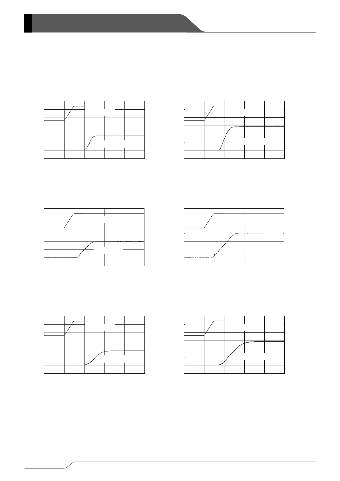
■TYPICAL PERFORMANCE CHARACTERISTICS (Continued)
(9) Output Turn-off Time with CE (Continued)
XC8101AA01
1.5
1.0
0.5
0.0
-0.5
-1.0
CE Input Voltage: VCE (V)
-1.5
-2.0
CE Input Voltage
Time: 10 μs/div
VIN=1.8V
CE=1. 2V→0.3V
tr=tf=5μs , IOUT=50mA
CIN=Non e , CL=0 .1μF
Output Voltage
6.0
5.0
4.0
3.0
2.0
1.0
0.0
-1.0
1.5
1.0
0.5
0.0
-0.5
-1.0
CE Input Voltage: VCE (V)
Output Voltage :VOUT (V)
-1.5
-2.0
XC8101AA01
CE Input Vo ltage
Output Voltage
Time: 10 μs/div
VIN=2.9V
CE=1. 2V→0.3V
tr=tf =5μs , IOUT=50mA
CIN=No ne , CL =0.1μF
6.0
5.0
4.0
3.0
2.0
1.0
0.0
-1.0
Output Voltage :VOUT ( V)
XC8101AA01
1.5
1.0
0.5
0.0
-0.5
-1.0
CE Input Voltage: VCE (V)
-1.5
-2.0
CE Input Voltage
Time: 1 0μs/div
VIN=4.0V
CE=1. 2V→0.3V
tr=tf =5μs , IOUT=50mA
CIN=Non e , CL =0 .1μF
Output Voltage
12.0
10.0
8.0
6.0
4.0
2.0
0.0
-2.0
1.5
1.0
0.5
0.0
-0.5
-1.0
CE Input Voltage: VCE (V)
Output Voltage :VOUT ( V)
-1.5
-2.0
XC8101AA01
CE Input Voltage
Time: 10 μs/div
VIN=6.0V
CE=1.2 V→0.3V
tr=tf =5μs , IOUT=50mA
CIN=None , CL=0.1μF
Output Voltage
12.0
10.0
8.0
6.0
4.0
2.0
0.0
-2.0
Output Voltage :VOUT (V)
XC8101AA01
1.5
1.0
0.5
0.0
-0.5
-1.0
CE Input Voltage: VCE (V)
-1.5
-2.0
CE Input Voltage
Time: 40 μs/div
VIN=1.8V
CE=1. 2V→0.3V
tr=tf=5μs , IOUT=50mA
CIN=Non e , CL=0 .47μF
Output Voltage
6.0
5.0
4.0
3.0
2.0
1.0
0.0
-1.0
1.5
1.0
0.5
0.0
-0.5
-1.0
CE Input Voltage: VCE (V)
Output Voltage :VOUT (V)
-1.5
-2.0
XC8101AA01
CE Input Vo ltage
Time: 40 μs/div
VIN=2.9V
CE=1. 2V→0.3V
tr=tf =5μs , IOUT=50mA
CIN=No ne , CL =0.4 7μF
Output Voltage
6.0
5.0
4.0
3.0
2.0
1.0
0.0
-1.0
Output Voltage :VOUT (V)
22/37

■TYPICAL PERFORMANCE CHARACTERISTICS (Continued)
(9) Output Turn-off Time with CE (Continued)
XC8101
Series
XC8101AA01
1.5
1.0
0.5
0.0
-0.5
-1.0
CE Input Voltage: VCE (V)
-1.5
-2.0
CE Input Voltage
Time: 10 0μs/div
VIN=4.0V
CE=1. 2V→0.3V
tr=tf =5μs , IOUT=50mA
CIN=Non e , CL =0 .4 7μF
Output Voltage
12.0
10.0
8.0
6.0
4.0
2.0
0.0
-2.0
1.5
1.0
0.5
0.0
-0.5
-1.0
CE Input Voltage: VCE (V)
Output Voltage :VOUT ( V)
-1.5
-2.0
XC8101AA01
CE Input Voltage
Time: 1 00 μs/div
VIN=6.0V
CE=1.2 V→0.3V
tr=tf =5μs , IOUT=50mA
CIN=None , CL=0.47μF
Output Voltage
12.0
10.0
8.0
6.0
4.0
2.0
0.0
-2.0
Output Voltage :VOUT ( V)
XC8101AA01
1.5
1.0
0.5
0.0
-0.5
-1.0
CE Input Voltage: VCE (V)
-1.5
-2.0
CE Input Voltage
Time: 1 00 μs/div
VIN=1.8V
CE=1. 2V→0.3V
tr=tf=5μs , IOUT=50mA
CIN=Non e, CL=1μF
Output Voltage
6.0
5.0
4.0
3.0
2.0
1.0
0.0
-1.0
1.5
1.0
0.5
0.0
-0.5
-1.0
CE Input Voltage: VCE (V)
Output Voltage :VOUT (V)
-1.5
-2.0
XC8101AA01
CE Input Vo ltage
Time: 1 00 μs/div
VIN=2.9V
CE=1. 2V→0.3V
tr=tf =5μs , IOUT=50mA
CIN=No ne , CL =1μF
Output Voltage
6.0
5.0
4.0
3.0
2.0
1.0
0.0
-1.0
Output Voltage :VOUT (V)
XC8101AA01
1.5
1.0
0.5
0.0
-0.5
-1.0
CE Input Voltage: VCE (V)
-1.5
-2.0
CE Input Voltage
Time: 20 0μs/div
VIN=4.0V
CE=1. 2V→0.3V
tr=tf =5μs , IOUT=50mA
CIN=Non e , CL =1μF
Output Voltage
12.0
10.0
8.0
6.0
4.0
2.0
0.0
-2.0
1.5
1.0
0.5
0.0
-0.5
-1.0
CE Input Voltage: VCE (V)
Output Voltage :VOUT ( V)
-1.5
-2.0
XC8101AA01
CE Input Voltage
Time: 2 00 μs/div
VIN=6.0V
CE=1.2 V→0.3V
tr=tf =5μs , IOUT=50mA
CIN=None, CL=1μF
Output Voltage
12.0
10.0
8.0
6.0
4.0
2.0
0.0
-2.0
Output Voltage :VOUT (V)
23/37

XC8101 Series
■TYPICAL PERFORMANCE CHARACTERISTICS (Continued)
(9) Output Turn-off Time with CE (Continued)
XC8101AA01
1.5
1.0
0.5
0.0
-0.5
-1.0
CE Input Voltage: VCE (V)
-1.5
-2.0
CE Input Voltage
Time: 10 μs/div
VIN=1.8V
CE=1. 2V→0.3V
tr=tf=5μs , IOUT=50mA
CIN=0.1μF , CL= 0.1μF
Output Voltage
6.0
5.0
4.0
3.0
2.0
1.0
0.0
-1.0
1.5
1.0
0.5
0.0
-0.5
-1.0
CE Input Voltage: VCE (V)
Output Voltage :VOUT (V)
-1.5
-2.0
XC8101AA01
CE Input Vo ltage
Output Voltage
Time: 10 μs/div
VIN=2.9V
CE=1. 2V→0.3V
tr=tf =5μs , IOUT=50mA
CIN=0. 1μF , CL=0.1μF
6.0
5.0
4.0
3.0
2.0
1.0
0.0
-1.0
Output Voltage :VOUT (V)
XC8101AA01
1.5
1.0
0.5
0.0
-0.5
-1.0
CE Input Voltage: VCE (V)
-1.5
-2.0
CE Input Voltage
Time: 2 0μs/div
VIN=4.0V
CE=1. 2V→0.3V
tr=tf =5μs , IOUT=50mA
CIN=0. 1μF , CL=0 .1μF
Output Voltage
12.0
10.0
8.0
6.0
4.0
2.0
0.0
-2.0
1.5
1.0
0.5
0.0
-0.5
-1.0
CE Input Voltage: VCE (V)
Output Voltage :VOUT ( V)
-1.5
-2.0
XC8101AA01
CE Input Voltage
Output Voltage
Time: 20 μs/div
VIN=6.0V
CE=1.2 V→0.3V
tr=tf =5μs , IOUT=50mA
CIN=0.1μF , CL=0. 1μF
12.0
10.0
8.0
6.0
4.0
2.0
0.0
-2.0
Output Voltage :VOUT (V)
XC8101AA01
1.5
1.0
0.5
0.0
-0.5
-1.0
CE Input Voltage: VCE (V)
-1.5
-2.0
CE Input Voltage
Time: 40 μs/div
VIN=1.8V
CE=1. 2V→0.3V
tr=tf=5μs , IOUT=50mA
CIN=0.1μF , CL= 0.4 7μF
Output Voltage
6.0
5.0
4.0
3.0
2.0
1.0
0.0
-1.0
1.5
1.0
0.5
0.0
-0.5
-1.0
CE Input Voltage: VCE (V)
Output Voltage :VOUT (V)
-1.5
-2.0
XC8101AA01
CE Input Vo ltage
Time: 1 00 μs/div
VIN=2.9V
CE=1. 2V→0.3V
tr=tf =5μs , IOUT=50mA
CIN=0. 1μF , CL=0.47μF
Output Voltage
6.0
5.0
4.0
3.0
2.0
1.0
0.0
-1.0
Output Voltage :VOUT (V)
24/37

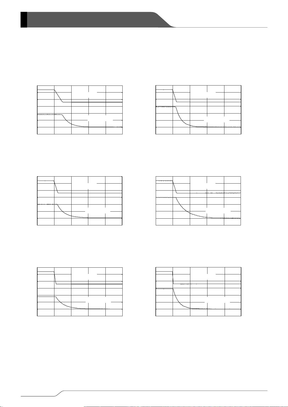
■TYPICAL PERFORMANCE CHARACTERISTICS (Continued)
(9) Output Turn-off Time with CE (Continued)
XC8101
Series
XC8101AA01
1.5
1.0
0.5
0.0
-0.5
-1.0
CE Input Voltage: VCE (V)
-1.5
-2.0
CE Input Voltage
Time: 10 0μs/div
VIN=4.0V
CE=1. 2V→0.3V
tr=tf =5μs , IOUT=50mA
CIN=0. 1μF , CL=0 .47μF
Output Voltage
12.0
10.0
8.0
6.0
4.0
2.0
0.0
-2.0
1.5
1.0
0.5
0.0
-0.5
-1.0
CE Input Voltage: VCE (V)
Output Voltage :VOUT ( V)
-1.5
-2.0
XC8101AA01
CE Input Voltage
Time: 1 00 μs/div
VIN=6.0V
CE=1.2 V→0.3V
tr=tf =5μs , IOUT=50mA
CIN=0.1μF , CL=0. 47μF
Output Voltage
12.0
10.0
8.0
6.0
4.0
2.0
0.0
-2.0
Output Voltage :VOUT (V)
XC8101AA01
1.5
1.0
0.5
0.0
-0.5
-1.0
CE Input Voltage: VCE (V)
-1.5
-2.0
CE Input Voltage
Output Voltage
Time: 1 00 μs/div
VIN=1.8V
CE=1. 2V→0.3V
tr=tf=5μs , IOUT=50mA
CIN=0.1μF , CL= 1μF
6.0
5.0
4.0
3.0
2.0
1.0
0.0
-1.0
1.5
1.0
0.5
0.0
-0.5
-1.0
CE Input Voltage: VCE (V)
Output Voltage :VOUT (V)
-1.5
-2.0
XC8101AA01
CE Input Vo ltage
Time: 1 00 μs/div
VIN=2.9V
CE=1. 2V→0.3V
tr=tf =5μs , IOUT=50mA
CIN=0. 1μF , CL= 1μF
Output Voltage
6.0
5.0
4.0
3.0
2.0
1.0
0.0
-1.0
Output Voltage :VOUT (V)
XC8101AA01
1.5
1.0
0.5
0.0
-0.5
-1.0
CE Input Voltage: VCE (V)
-1.5
-2.0
CE Input Voltage
Time: 20 0μs/div
VIN=4.0V
CE=1. 2V→0.3V
tr=tf =5μs , IOUT=50mA
CIN=0. 1μF , CL=1μF
Output Voltage
12.0
10.0
8.0
6.0
4.0
2.0
0.0
-2.0
1.5
1.0
0.5
0.0
-0.5
-1.0
CE Input Voltage: VCE (V)
Output Voltage :VOUT ( V)
-1.5
-2.0
XC8101AA01
CE Input Voltage
Time: 2 00 μs/div
VIN=6.0V
CE=1.2 V→0.3V
tr=tf =5μs , IOUT=50mA
CIN=0.1μF , CL=1μF
Output Voltage
12.0
10.0
8.0
6.0
4.0
2.0
0.0
-2.0
Output Voltage :VOUT (V)
25/37

XC8101 Series
■TYPICAL PERFORMANCE CHARACTERISTICS (Continued)
(9) Output Turn-off Time with CE (Continued)
XC8101AA01
1.5
1.0
0.5
0.0
-0.5
-1.0
CE Input Voltage: VCE (V)
-1.5
-2.0
CE Input Voltage
Time: 20 μs/div
VIN=1.8V
CE=1. 2V→0.3V
tr=tf=5μs , IOUT=50mA
CIN=0.2 2μF , CL=0.1μF
Output Voltage
6.0
5.0
4.0
3.0
2.0
1.0
0.0
-1.0
1.5
1.0
0.5
0.0
-0.5
-1.0
CE Input Voltage: VCE (V)
Output Voltage :VOUT (V)
-1.5
-2.0
XC8101AA01
CE Input Vo ltage
Output Voltage
Time: 20 μs/div
VIN=2.9V
CE=1. 2V→0.3V
tr=tf =5μs , IOUT=50mA
CIN=0. 22μF , CL=0.1μF
6.0
5.0
4.0
3.0
2.0
1.0
0.0
-1.0
Output Voltage :VOUT (V)
XC8101AA01
1.5
1.0
0.5
0.0
-0.5
-1.0
CE Input Voltage: VCE (V)
-1.5
-2.0
CE Input Voltage
Output Voltage
Time: 2 0μs/div
VIN=4.0V
CE=1. 2V→0.3V
tr=tf =5μs , IOUT=50mA
CIN=0. 22μF , CL=0.1μF
12.0
10.0
8.0
6.0
4.0
2.0
0.0
-2.0
1.5
1.0
0.5
0.0
-0.5
-1.0
CE Input Voltage: VCE (V)
Output Voltage :VOUT ( V)
-1.5
-2.0
XC8101AA01
CE Input Voltage
Output Voltage
Time: 20 μs/div
VIN=6.0V
CE=1.2 V→0.3V
tr=tf =5μs , IOUT=50mA
CIN=0.22μF , CL= 0.1μF
12.0
10.0
8.0
6.0
4.0
2.0
0.0
-2.0
Output Voltage :VOUT ( V)
XC8101AA01
1.5
1.0
0.5
0.0
-0.5
-1.0
CE Input Voltage: VCE (V)
-1.5
-2.0
CE Input Voltage
Time: 40 μs/div
VIN=1.8V
CE=1. 2V→0.3V
tr=tf=5μs , IOUT=50mA
CIN=0.2 2μF , CL=0.47μF
Output Voltage
6.0
5.0
4.0
3.0
2.0
1.0
0.0
-1.0
1.5
1.0
0.5
0.0
-0.5
-1.0
CE Input Voltage: VCE (V)
Output Voltage :VOUT (V)
-1.5
-2.0
XC8101AA01
CE Input Vo ltage
Time: 1 00 μs/div
VIN=2.9V
CE=1. 2V→0.3V
tr=tf =5μs , IOUT=50mA
CIN=0. 22μF , CL=0.47μF
Output Voltage
6.0
5.0
4.0
3.0
2.0
1.0
0.0
-1.0
Output Voltage :VOUT (V)
26/37

■TYPICAL PERFORMANCE CHARACTERISTICS (Continued)
(9) Output Turn-off Time with CE (Continued)
XC8101
Series
XC8101AA01
1.5
1.0
0.5
0.0
-0.5
-1.0
CE Input Voltage: VCE (V)
-1.5
-2.0
CE Input Voltage
Time: 10 0μs/div
VIN=4.0V
CE=1. 2V→0.3V
tr=tf =5μs , IOUT=50mA
CIN=0. 22μF , CL=0.47μF
Output Voltage
12.0
10.0
8.0
6.0
4.0
2.0
0.0
-2.0
1.5
1.0
0.5
0.0
-0.5
-1.0
CE Input Voltage: VCE (V)
Output Voltage :VOUT ( V)
-1.5
-2.0
XC8101AA01
CE Input Voltage
Time: 1 00 μs/div
VIN=6.0V
CE=1.2 V→0.3V
tr=tf =5μs , IOUT=50mA
CIN=0.22μF , CL= 0.4 7μF
Output Voltage
12.0
10.0
8.0
6.0
4.0
2.0
0.0
-2.0
Output Voltage :VOUT (V)
XC8101AA01
1.5
1.0
0.5
0.0
-0.5
-1.0
CE Input Voltage: VCE (V)
-1.5
-2.0
CE Input Voltage
Time: 1 00 μs/div
VIN=1.8V
CE=1. 2V→0.3V
tr=tf=5μs , IOUT=50mA
CIN=0.2 2μF , CL= 1μF
Output Voltage
6.0
5.0
4.0
3.0
2.0
1.0
0.0
-1.0
1.5
1.0
0.5
0.0
-0.5
-1.0
CE Input Voltage: VCE (V)
Output Voltage :VOUT (V)
-1.5
-2.0
XC8101AA01
CE Input Vo ltage
Time: 2 00 μs/div
VIN=2.9V
CE=1. 2V→0.3V
tr=tf =5μs , IOUT=50mA
CIN=0. 22μF , CL=1μF
Output Voltage
6.0
5.0
4.0
3.0
2.0
1.0
0.0
-1.0
Output Voltage :VOUT (V)
XC8101AA01
1.5
1.0
0.5
0.0
-0.5
-1.0
CE Input Voltage: VCE (V)
-1.5
-2.0
CE Input Voltage
Time: 20 0μs/div
VIN=4.0V
CE=1. 2V→0.3V
tr=tf =5μs , IOUT=50mA
CIN=0. 22μF , CL= 1μF
Output Voltage
12.0
10.0
8.0
6.0
4.0
2.0
0.0
-2.0
1.5
1.0
0.5
0.0
-0.5
-1.0
CE Input Voltage: VCE (V)
Output Voltage :VOUT ( V)
-1.5
-2.0
XC8101AA01
CE Input Voltage
Time: 2 00 μs/div
VIN=6.0V
CE=1.2 V→0.3V
tr=tf =5μs , IOUT=50mA
CIN=0.22μF , CL= 1μF
Output Voltage
12.0
10.0
8.0
6.0
4.0
2.0
0.0
-2.0
Output Voltage :VOUT (V)
27/37

XC8101 Series
■TYPICAL PERFORMANCE CHARACTERISTICS (Continued)
(9) Output Turn-off Time with CE (Continued)
XC8101AA01
1.5
1.0
0.5
0.0
-0.5
-1.0
CE Input Voltage: VCE (V)
-1.5
-2.0
CE Input Voltage
Time: 20 μs/div
VIN=1.8V
CE=1. 2V→0.3V
tr=tf=5μs , IOUT=50mA
CIN=0.4 7μF , CL=0.1μF
Output Voltage
6.0
5.0
4.0
3.0
2.0
1.0
0.0
-1.0
1.5
1.0
0.5
0.0
-0.5
-1.0
CE Input Voltage: VCE (V)
Output Voltage :VOUT (V)
-1.5
-2.0
XC8101AA01
CE Input Vo ltage
Output Voltage
Time: 20 μs/div
VIN=2.9V
CE=1. 2V→0.3V
tr=tf =5μs , IOUT=50mA
CIN=0. 47μF , CL=0.1μF
6.0
5.0
4.0
3.0
2.0
1.0
0.0
-1.0
Output Voltage :VOUT (V)
XC8101AA01
1.5
1.0
0.5
0.0
-0.5
-1.0
CE Input Voltage: VCE (V)
-1.5
-2.0
CE Input Voltage
Time: 2 0μs/div
VIN=4.0V
CE=1. 2V→0.3V
tr=tf =5μs , IOUT=50mA
CIN=0. 47μF , CL=0.1μF
Output Voltage
12.0
10.0
8.0
6.0
4.0
2.0
0.0
-2.0
1.5
1.0
0.5
0.0
-0.5
-1.0
CE Input Voltage: VCE (V)
Output Voltage :VOUT ( V)
-1.5
-2.0
XC8101AA01
CE Input Voltage
Output Voltage
Time: 20 μs/div
VIN=6.0V
CE=1.2 V→0.3V
tr=tf =5μs , IOUT=50mA
CIN=0.47μF , CL= 0.1μF
12.0
10.0
8.0
6.0
4.0
2.0
0.0
-2.0
Output Voltage :VOUT (V)
1.5
1.0
0.5
0.0
-0.5
-1.0
CE Input Voltage: VCE (V)
-1.5
-2.0
28/37
XC8101AA01
CE Input Voltage
Outpu t V oltag e
Time: 40 μs/div
VIN=1.8V
CE=1. 2V→0.3V
tr=tf=5μs , IOUT=50mA
CIN=0.4 7μF , CL=0.47μF
6.0
5.0
4.0
3.0
2.0
1.0
0.0
-1.0
XC8101AA01
1.5
1.0
0.5
0.0
-0.5
-1.0
CE Input Voltage: VCE (V)
Output Voltage :VOUT (V)
-1.5
-2.0
CE Input Vo ltage
Time: 1 00 μs/div
VIN=2.9V
CE=1. 2V→0.3V
tr=tf =5μs , IOUT=50mA
CIN=0. 47μF , CL=0.47μF
Output Voltage
6.0
5.0
4.0
3.0
2.0
1.0
0.0
-1.0
Output Voltage :VOUT (V)

■TYPICAL PERFORMANCE CHARACTERISTICS (Continued)
(9) Output Turn-off Time with CE (Continued)
XC8101
Series
XC8101AA01
1.5
1.0
0.5
0.0
-0.5
-1.0
CE Input Voltage: VCE (V)
-1.5
-2.0
CE Input Voltage
Time: 10 0μs/div
VIN=4.0V
CE=1. 2V→0.3V
tr=tf =5μs , IOUT=50mA
CIN=0. 47μF , CL=0.47μF
Output Voltage
12.0
10.0
8.0
6.0
4.0
2.0
0.0
-2.0
1.5
1.0
0.5
0.0
-0.5
-1.0
CE Input Voltage: VCE (V)
Output Voltage :VOUT ( V)
-1.5
-2.0
XC8101AA01
CE Input Voltage
Time: 1 00 μs/div
VIN=6.0V
CE=1.2 V→0.3V
tr=tf =5μs , IOUT=50mA
CIN=0.47μF , CL= 0.4 7μF
Output Voltage
12.0
10.0
8.0
6.0
4.0
2.0
0.0
-2.0
Output Voltage :VOUT ( V)
XC8101AA01
1.5
1.0
0.5
0.0
-0.5
-1.0
CE Input Voltage: VCE (V)
-1.5
-2.0
CE Input Voltage
Time: 1 00 μs/div
VIN=1.8V
CE=1. 2V→0.3V
tr=tf=5μs , IOUT=50mA
CIN=0.4 7μF , CL= 1μF
Output Voltage
6.0
5.0
4.0
3.0
2.0
1.0
0.0
-1.0
1.5
1.0
0.5
0.0
-0.5
-1.0
CE Input Voltage: VCE (V)
Output Voltage :VOUT (V)
-1.5
-2.0
XC8101AA01
CE Input Vo ltage
Time: 1 00 μs/div
VIN=2.9V
CE=1. 2V→0.3V
tr=tf =5μs , IOUT=50mA
CIN=0. 47μF , CL=1μF
Output Voltage
6.0
5.0
4.0
3.0
2.0
1.0
0.0
-1.0
Output Voltage :VOUT (V)
XC8101AA01
1.5
1.0
0.5
0.0
-0.5
-1.0
CE Input Voltage: VCE (V)
-1.5
-2.0
CE Input Voltage
Time: 20 0μs/div
VIN=4.0V
CE=1. 2V→0.3V
tr=tf =5μs , IOUT=50mA
CIN=0. 47μF , CL= 1μF
Output Voltage
12.0
10.0
8.0
6.0
4.0
2.0
0.0
-2.0
1.5
1.0
0.5
0.0
-0.5
-1.0
CE Input Voltage: VCE (V)
Output Voltage :VOUT ( V)
-1.5
-2.0
XC8101AA01
CE Input Voltage
Time: 2 00 μs/div
VIN=6.0V
CE=1.2 V→0.3V
tr=tf =5μs , IOUT=50mA
CIN=0.47μF , CL= 1μF
Output Voltage
12.0
10.0
8.0
6.0
4.0
2.0
0.0
-2.0
Output Voltage :VOUT (V)
29/37
XC8101 Series
■TYPICAL PERFORMANCE CHARACTERISTICS (Continued)
(9) Output Turn-off Time with CE (Continued)
XC8101AA01
1.5
1.0
0.5
0.0
-0.5
-1.0
CE Input Voltage: VCE (V)
-1.5
-2.0
CE Input Voltage
Time: 10 μs/div
VIN=1.8V
CE=1. 2V→0.3V
tr=tf=5μs , IOUT=50mA
CIN=1μF , CL= 0.1μF
Output Voltage
6.0
5.0
4.0
3.0
2.0
1.0
0.0
-1.0
1.5
1.0
0.5
0.0
-0.5
-1.0
CE Input Voltage: VCE (V)
Output Voltage :VOUT (V)
-1.5
-2.0
XC8101AA01
CE Input Vo ltage
Output Voltage
Time: 20 μs/div
VIN=2.9V
CE=1. 2V→0.3V
tr=tf =5μs , IOUT=50mA
CIN=1μF , CL=0.1μF
6.0
5.0
4.0
3.0
2.0
1.0
0.0
-1.0
Output Voltage :VOUT (V)
XC8101AA01
1.5
1.0
0.5
0.0
-0.5
-1.0
CE Input Voltage: VCE (V)
-1.5
-2.0
CE Input Voltage
Time: 2 0μs/div
VIN=4.0V
CE=1. 2V→0.3V
tr=tf =5μs , IOUT=50mA
CIN=1μF , CL=0.1μF
Output Voltage
12.0
10.0
8.0
6.0
4.0
2.0
0.0
-2.0
1.5
1.0
0.5
0.0
-0.5
-1.0
CE Input Voltage: VCE (V)
Output Voltage :VOUT ( V)
-1.5
-2.0
XC8101AA01
CE Input Voltage
Time: 20 μs/div
VIN=6.0V
CE=1.2 V→0.3V
tr=tf =5μs , IOUT=50mA
CIN=1μF , CL=0.1μF
Output Voltage
12.0
10.0
8.0
6.0
4.0
2.0
0.0
-2.0
Output Voltage :VOUT (V)
1.5
1.0
0.5
0.0
-0.5
-1.0
CE Input Voltage: VCE (V)
-1.5
-2.0
30/37
XC8101AA01
CE Input Voltage
Output Voltage
Time: 40 μs/div
VIN=1.8V
CE=1. 2V→0.3V
tr=tf=5μs , IOUT=50mA
CIN=1μF , CL= 0.4 7μF
6.0
5.0
4.0
3.0
2.0
1.0
0.0
-1.0
XC8101AA01
1.5
1.0
0.5
0.0
-0.5
-1.0
CE Input Voltage: VCE (V)
Output Voltage :VOUT (V)
-1.5
-2.0
CE Input Vo ltage
Time: 1 00 μs/div
VIN=2.9V
CE=1. 2V→0.3V
tr=tf =5μs , IOUT=50mA
CIN=1μF , CL=0.47μF
Output Voltage
6.0
5.0
4.0
3.0
2.0
1.0
0.0
-1.0
Output Voltage :VOUT (V)

■TYPICAL PERFORMANCE CHARACTERISTICS (Continued)
(9) Output Turn-off Time with CE (Continued)
XC8101
Series
XC8101AA01
1.5
1.0
0.5
0.0
-0.5
-1.0
CE Input Voltage: VCE (V)
-1.5
-2.0
CE Input Voltage
Time: 10 0μs/div
VIN=4.0V
CE=1. 2V→0.3V
tr=tf =5μs , IOUT=50mA
CIN=1μF , CL=0.47μF
Output Voltage
12.0
10.0
8.0
6.0
4.0
2.0
0.0
-2.0
1.5
1.0
0.5
0.0
-0.5
-1.0
CE Input Voltage: VCE (V)
Output Voltage :VOUT ( V)
-1.5
-2.0
XC8101AA01
CE Input Voltage
Time: 1 00 μs/div
VIN=6.0V
CE=1.2 V→0.3V
tr=tf =5μs , IOUT=50mA
CIN=1μF , CL=0.47μF
Output Voltage
12.0
10.0
8.0
6.0
4.0
2.0
0.0
-2.0
Output Voltage :VOUT (V)
XC8101AA01
1.5
1.0
0.5
0.0
-0.5
-1.0
CE Input Voltage: VCE (V)
-1.5
-2.0
CE Input Voltage
Time: 1 00 μs/div
VIN=1.8V
CE=1. 2V→0.3V
tr=tf=5μs , IOUT=50mA
CIN=1μF , CL= 1μF
Output Voltage
6.0
5.0
4.0
3.0
2.0
1.0
0.0
-1.0
1.5
1.0
0.5
0.0
-0.5
-1.0
CE Input Voltage: VCE (V)
Output Voltage :VOUT (V)
-1.5
-2.0
XC8101AA01
CE Input Vo ltage
Time: 1 00 μs/div
VIN=2.9V
CE=1. 2V→0.3V
tr=tf =5μs , IOUT=50mA
CIN=1μF , CL= 1μF
Output Voltage
6.0
5.0
4.0
3.0
2.0
1.0
0.0
-1.0
Output Voltage :VOUT (V)
XC8101AA01
1.5
1.0
0.5
0.0
-0.5
-1.0
CE Input Voltage: VCE (V)
-1.5
-2.0
CE Input Voltage
Time: 20 0μs/div
VIN=4.0V
CE=1. 2V→0.3V
tr=tf =5μs , IOUT=50mA
CIN=1μF , CL= 1μF
Output Voltage
12.0
10.0
8.0
6.0
4.0
2.0
0.0
-2.0
1.5
1.0
0.5
0.0
-0.5
-1.0
CE Input Voltage: VCE (V)
Output Voltage :VOUT ( V)
-1.5
-2.0
XC8101AA01
CE Input Voltage
Time: 2 00 μs/div
VIN=6.0V
CE=1.2 V→0.3V
tr=tf =5μs , IOUT=50mA
CIN=1μF , CL= 1μF
Output Voltage
12.0
10.0
8.0
6.0
4.0
2.0
0.0
-2.0
Output Voltage :VOUT (V)
31/37

XC8101 Series
■PACKAGING INFORMATION
●SOT-25
●USP-4
32/37
Unit : mm
Unit : mm
●SSOT-24
Unit : mm

XC8101
Series
■PACKAGING INFORMATION (Continued)
● SOT-25 Power Dissipation
Power dissipation data for the SOT-25 is shown in this page.
The value of power dissipation varies with the mount board conditions.
Please use this data as one of reference data taken in the described condition.
1. Measurement Condition (Reference data)
Condition: Mount on a board
Ambient: Natural convection
Soldering: Lead (Pb) free
Board: Dimensions 40 x 40 mm (1600 mm
Copper (Cu) traces occupy 50% of the board area
In top and back faces
Package heat-sink is tied to the copper traces
(Board of SOT-26 is used)
Material:Glass Epoxy (FR-4)
Thickness: 1.6 mm
Through-hole: 4 x 0.8 Diameter
2
in one side)
2. Power Dissipation vs. Ambient Temperature
Board Mount (Tj max = 125℃)
Evaluation Board (Unit: mm)
評価基板レイアウト(単位:mm)
Ambient Temperature(℃) Power Dissipation Pd(mW) Thermal Resistance (℃/W)
25 600
166.67
85 240
Pd-Ta特性グラフ
Pd vs. Ta
700
600
500
400
300
200
100
許容損失Pd(mW)
Power Dissipation Pd (mW)
0
25 45 65 85 105 125
Ambient Temperature Ta (℃)
周辺温度Ta(℃)
33/37

mW
XC8101 Series
■PACKAGING INFORMATION (Continued)
● SSOT-24 Power Dissipation
Power dissipation data for the SSOT-24 is shown in this page.
The value of power dissipation varies with the mount board conditions.
Please use this data as one of reference data taken in the described condition.
2. Measurement Condition (Reference data)
Condition: Mount on a board
Ambient: Natural convection
Soldering: Lead (Pb) free
Board: Dimensions 40 x 40 mm (1600 mm
Copper (Cu) traces occupy 50% of the board area
In top and back faces
Package heat-sink is tied to the copper traces
Material: Glass Epoxy (FR-4)
Thickness: 1.6 mm
Through-hole: 4 x 0.8 Diameter
2. Power Dissipation vs. Ambient Temperature
Board Mount (Tj max = 125℃)
2
in one side)
28.9
40.0
28.9
1.4
2.54
Evaluation Board (Unit: mm)
40.0
2.5
Ambient Temperature(℃) Power Dissipation Pd(mW) Thermal Resistance (℃/W)
25 500
200.00
85 200
600
500
400
300
200
許容損失P d(
100
0
Power Dissipation Pd (mW)
25 45 65 85 105 125
Pd-Ta特性グラフ
Pd vs. Ta
Ambient Temperature Ta (℃)
周辺温度Ta (℃)
34/37

■PACKAGING INFORMATION (Continued)
● USP-4 Power Dissipation
Power dissipation data for the USP-4 is shown in this page.
The value of power dissipation varies with the mount board conditions.
Please use this data as one of reference data taken in the described condition.
1. Measurement Condition (Reference data)
Condition: Mount on a board
Ambient: Natural convection
Soldering: Lead (Pb) free
Board: Dimensions 40 x 40 mm (1600 mm
Copper (Cu) traces occupy 50% of the board area
In top and back faces
Package heat-sink is tied to the copper traces
Material: Glass Epoxy (FR-4)
Thickness: 1.6 mm
Through-hole: 4 x 0.8 Diameter
2. Power Dissipation vs. Ambient Temperature
Board Mount (Tj max = 125℃)
2
in one side)
28.9
Evaluation Board (Unit: mm)
XC8101
Series
40.0
2.5
Ambient Temperature(℃) Power Dissipation Pd(mW) Thermal Resistance (℃/W)
25 1000
100.00
85 400
1200
1000
800
600
400
200
Power Dissipation Pd (mW)
0
25 45 65 85 105 125
Pd vs Ta
Ambient Temperature Ta(℃)
35/37

XC8101 Series
■MARKING RULE
●SOT-25、USP-4
① represents product series
MARK PRODUCT SERIES
U XC8101******
② represents CE pin logic
MARK PRODUCT SERIES
F XC8101A*****
③ represents CL Discharge Function
MARK PRODUCT SERIES
C XC8101AA****
④⑤ represents production lot number
01, …,09, 0A, …,0Z, 11,…,9Z, A1, …, A9, AA, …, Z9, ZA,…,ZZ repeated.
(G, I, J, O, Q, W excluded)
*No character inversion used.
●SSOT-24
① represents product series
MARK PRODUCT SERIES
U XC8101******
② represents CE pin logic
MARK PRODUCT SERIES
F XC8101A*****
③④ represents production lot number
01, …,09, 0A, …,0Z, 11,…,9Z, A1, …, A9, AA, …, Z9, ZA,…,ZZ repeated.
(G, I, J, O, Q, W excluded)
*No character inversion used.
SOT-25
(TOP VIEW)
SSOT-24
(TOP VIEW)
USP-4
(TOP VIEW)
36/37

XC8101
Series
1. The products and product specifications contained herein are subject to change without
notice to improve performance characteristics. Consult us, or our representatives
before use, to confirm that the information in this datasheet is up to date.
2. We assume no responsibility for any infringement of patents, patent rights, or other
rights arising from the use of any information and circuitry in this datasheet.
3. Please ensure suitable shipping controls (including fail-safe designs and aging
protection) are in force for equipment employing products listed in this datasheet.
4. The products in this datasheet are not developed, designed, or approved for use with
such equipment whose failure of malfunction can be reasonably expected to directly
endanger the life of, or cause significant injury to, the user.
(e.g. Atomic energy; aerospace; transport; combustion and associated safety
equipment thereof.)
5. Please use the products listed in this datasheet within the specified ranges.
Should you wish to use the products under conditions exceeding the specifications,
please consult us or our representatives.
6. We assume no responsibility for damage or loss due to abnormal use.
7. All rights reserved. No part of this datasheet may be copied or reproduced without the
prior permission of TOREX SEMICONDUCTOR LTD.
37/37
 Loading...