


Torex XC6219A091MR, XC6219A091PR, XC6219A092MR, XC6219A092PR, XC6219A101MR Schematic [ru]
...XC6219/XC6211Series
ETR0307_009
300mA High Speed LDO Regulators with ON/OFF Switch
■GENERAL DESCRIPTION
The XC6219/XC6211 series are highly accurate, low noise, CMOS LDO Voltage Regulators. Offering low output noise, high ripple rejection ratio, low dropout and very fast turn-on times, the XC6219/XC6211 series is ideal for today’s cutting edge mobile phone.
Internally the XC6219/XC6211 includes a reference voltage source, error amplifiers, driver transistors, current limiters and phase compensators. The XC6219/XC6211’s current limiters' foldback circuit also operates as a short protect for the output current limiter and. the output pin. The output voltage is set by laser trimming. Voltages are selectable in 50mV steps within a range of 0.9V to 5.0V. The XC6219/XC6211 series is also fully compatible with low ESR ceramic capacitors, reducing cost and improving output stability. This high level of output stability is maintained even during frequent load fluctuations, due to the excellent transient response performance and high PSRR achieved across a broad range of frequencies.
The CE function allows the output of regulator to be turned off, resulting in greatly reduced power consumption.
■APPLICATIONS
●Mobile phones
●Cordless phones, radio communication equipment ●Portable games
●Cameras, Video cameras ●Reference voltage sources ●Battery powered equipment
■FEATURES
Maximum Output Current |
: 150mA (VOUT<1.75V, A~D type) |
||
|
240mA (VOUT>1.8V, A~D type) |
||
|
|
|
|
|
300mA (VOUT>1.3V, E~H type) |
||
Dropout Voltage |
|
|
|
: 200mV @ 100mA |
|||
Operating Voltage Range |
: 2.0V ~ 6.0V |
||
Output Voltage Range |
: 0.9V ~ 5.0V (0.05V steps) |
||
Highly Accuracy |
: +2% (VOUT>1.5V) |
||
|
+30mV (VOUT 1.5V) |
||
|
+1% (VOUT 3.0V) |
||
Low Power Consumption |
: 25μA (TYP.) |
||
Standby Current |
: Less than 0.1μA (TYP.) |
||
High Ripple Rejection |
: 65dB @10kHz |
||
Operating Ambient Temperature |
: -40 ~ 85 |
||
Low ESR Capacitor |
: Ceramic capacitor compatible |
||
Ultra Small Packages |
: SOT-25 |
||
|
SOT-89-5 (for XC6219 only) |
||
Environmentally Friendly |
USP-6B (for XC6219 only) |
||
: EU RoHS Compliant, Pb Free |
|||
■TYPICAL APPLICATION CIRCUIT ■TYPICAL PERFORMANCE
●XC6219 series |
|
|
|
|
|
|
|
|
|
|
CHARACTERISTICS |
||||||||||||||||
|
|
|
|
|
|
|
|
|
|
●Ripple Rejection Rate |
|||||||||||||||||
|
|
|
|
|
|
|
|
|
|
|
|
|
|
|
|
|
|
|
|
|
|
|
|
|
|
|
XC6219/XC6211 |
|
|
|
|
|
|
|
|
|
|
|
|
|
|
|
|
|
|
|
|
|
|
|
|
|
|
|
|
|
|
|
|
|
|
|
|
|
|
|
|
|
|
|
|
|
|
VIN |
VOUT |
5 |
|
|
|
|
|
|
|
|
|
|
|
|
|
|
|
|
|
|
|
|
|
|
|
1 |
|
|
|
|
|
|
|
|
|||
|
|
|
|
|
|
|
|
|
|
|
|
|
|
|
|
|
|
|
|
|
|
CL |
|||||
|
|
|
|
|
|
|
|
|
|
|
|
|
|
|
|
|
|
|
|
|
|
|
|
|
|
||
|
|
|
|
|
|
|
|
|
|
|
|
|
|
|
|
|
|
|
|
|
|
|
|
|
|
||
|
|
|
|
|
|
|
|
|
|
|
|
|
|
|
|
|
|
|
|
|
|
|
|
|
|
||
|
|
|
|
|
|
|
|
|
|
|
|
|
|
|
|
2 |
|
VSS |
|
|
|
|
|
|
|
μ |
|
|
|
|
|
|
|
|
|
|
|
|
|
|
|
|
|
|
|
CE |
NC |
|
|
|
|
|
|
1 F |
|
|
|
|
|
|
|
|
|
|
|
|
|
|
|
|
|
|
|
|
|
|
|
|
|
|
|||
|
|
|
|
|
|
|
|
|
|
|
|
|
|
|
|
|
|
|
|
|
|
|
|
|
|
||
|
|
|
|
|
|
|
|
|
|
|
|
|
|
|
|
|
|
|
|
|
|
|
|
|
|
||
|
|
|
|
|
|
|
|
|
|
|
|
|
|
|
|
3 |
|
4 |
|
|
|
|
|
|
|
||
|
|
|
|
|
|
|
|
|
|
|
|
|
|
|
|
|
|
|
|
|
|
|
|
||||
|
|
|
|
|
|
|
|
|
|
|
|
CIN |
|
|
|
|
|
|
|
|
|
|
|
||||
|
|
|
|
|
|
|
|
|
|
|
|
|
|
|
|
|
|
|
|
|
|
|
|||||
|
|
|
|
|
|
|
|
|
|
|
|
|
|
|
|
|
|
|
|
|
|||||||
|
|
|
|
|
|
|
|
|
|
|
|
|
μ |
|
|
|
|
|
|
|
|
|
|
|
|||
|
|
|
|
|
|
|
|
|
|
|
|
1 F |
|
|
|
|
|
|
|
|
|
|
|
||||
|
|
|
|
|
|
|
|
|
|
|
|
|
|
|
|
|
SOT-25 |
|
|
|
|
|
|
|
|
||
1/30

 XC6219/XC6211 Series
■PIN CONFIGURATION
[XC6219 Series] |
|
|
|
VOUT |
VSS |
VIN |
|
|
|
|
|
|
|
|
|
||||||||||||||
|
|
|
|
|
|
|
|
|
|
|
|
|
|
|
|
|
|
|
|
|
|
|
|
|
|
|
|
|
|
|
VOUT |
|
|
|
NC |
|
|
|
|
5 |
|
2 |
|
|
4 |
|
|
|
|
|
|
|
|
|
|
|
|||
|
|
|
|
|
|
|
|
|
|
|
|
|
|
|
|
|
|
|
|
||||||||||
|
|
5 |
|
|
|
|
4 |
|
|
|
|
|
|
|
|
|
|
|
|
|
CE 6 |
|
|
|
|
|
|
|
1 VIN |
|
|
|
|
|
|
|
|
|
|
|
|
|
|
|
|
|
|
|
|
|
|
|
|
|
|
||||
|
|
|
|
|
|
|
|
|
|
|
|
|
|
|
|
|
|
|
|
|
|
|
|
|
|
||||
|
|
|
|
|
|
|
|
|
|
|
|
|
|
|
|
|
|
|
|
|
|
|
|
|
|
|
|
||
|
|
|
|
|
|
|
|
|
|
|
|
|
|
|
|
|
|
|
|
|
|
|
|
|
|
|
|
||
|
|
|
|
|
|
|
|
|
|
|
|
|
|
|
|
|
|
|
|
|
|
|
|
|
|
|
|
||
|
|
|
|
|
|
|
|
|
|
|
|
|
|
|
|
|
|
|
|
|
VSS 5 |
|
|
|
|
|
|
|
2 NC |
|
|
|
|
|
|
|
|
|
|
|
|
|
|
|
|
|
|
|
|
|
|
|
|
|
|
|
|
||
|
|
|
|
|
|
|
|
|
|
|
|
|
|
|
|
|
|
|
|
|
|
|
|
|
|
|
|
||
|
|
|
|
|
|
|
|
|
|
|
|
|
|
|
|
|
|
|
|
|
NC 4 |
|
|
|
|
|
|
|
3 VOUT |
|
|
1 |
|
|
2 |
|
3 |
|
|
|
|
1 |
|
|
2 |
|
|
3 |
|
|
|
|
|
|
|
|
|
|
|
|
|
|
|
|
|
|
|
|
|
|
|
|
|
|
|
|
|
|
|
|
|
|
|
||||||
|
VIN |
VSS CE |
|
|
|
|
|
|
|
|
|
|
|
|
|
|
|
|
|
|
|
||||||||
|
|
|
|
|
|
|
|
|
|
|
|
|
|
|
|
|
|
|
|
|
|
||||||||
|
|
|
|
NC |
VSS |
CE |
|
|
|
|
|
|
|
|
|
||||||||||||||
|
|
|
|
SOT-25 |
|
|
|
|
|
|
|
SOT-89-5 |
|
|
|
|
|
|
USP-6B |
||||||||||
|
|
(TOP VIEW) |
|
|
|
|
|
|
(TOP VIEW) |
(BOTTOM VIEW) |
|||||||||||||||||||
* The dissipation pad for the USP-6B package should be solder-plated in recommended mount pattern and metal masking so as to enhance mounting strength and hear release. If the pad needs to be connected to other pins, it should be connected to the VSS pin.
[XC6211 Series]
VIN |
|
|
VOUT |
||||
|
5 |
|
|
|
4 |
|
|
|
|
|
|
|
|
|
|
|
|
|
|
|
|
|
|
|
|
|
|
|
|
|
|
1 |
|
|
2 |
|
3 |
|
CE |
VSS |
NC |
||||
SOT-25
(TOP VIEW)
■PIN ASSIGNMENT
|
PIN NUMBER |
|
|
|
|
|
|
|
|
XC6211 |
|
XC6219 |
|
|
PIN NAME |
|
|
FUNCTIONS |
|
SOT-25 |
SOT-25 |
SOT-89-5 |
USP-6B |
|
|
|
|
|
|
5 |
1 |
4 |
1 |
|
VIN |
|
Power Input |
||
2 |
2 |
2 |
5 |
|
VSS |
|
Ground |
||
1 |
3 |
3 |
6 |
|
CE |
|
ON / OFF Control |
||
3 |
4 |
1 |
2, 4 |
|
NC |
|
No Connection |
||
4 |
5 |
5 |
3 |
|
VOUT |
|
Output |
||
■FUNCTION
TYPE A,E
|
PIN NAME |
SIGNAL |
STATUS |
|
|
L |
Stand-by |
|
|
|
|
|
CE |
H |
Active |
|
|
OPEN |
Stand-by |
|
|
|
|
TYPE C,G |
|
|
|
|
PIN NAME |
SIGNAL |
STATUS |
|
|
L |
Active |
|
CE |
H |
Stand-by |
|
|
|
|
|
|
OPEN |
Stand-by |
|
|
|
|
TYPE B,F
|
|
PIN NAME |
SIGNAL |
|
STATUS |
|
|
|
|
L |
|
Stand-by |
|
|
|
|
|
|
|
|
|
|
CE |
H |
|
Active |
|
|
|
|
OPEN |
|
Undefined state |
|
|
|
|
|
|
|
|
|
|
TYPE D,H |
|
|
|
|
|
|
PIN NAME |
SIGNAL |
|
STATUS |
|
|
|
|
L |
|
Active |
|
|
|
CE |
H |
|
Stand-by |
|
|
|
|
|
|
|
|
|
|
|
OPEN |
|
Undefined state |
|
|
|
|
|
|
|
|
*If XC6211/XC6219 B,D,F,H types are used with the CE pin opened, the IC goes into “Undefined state”. The CE pin voltage should be fixed in low or high for stable operation.
2/30

XC6219/XC6211
Series
■PRODUCT CLASSIFICATION
●Ordering Information
XC6219 - (*1)(Standard pin layout versions) XC6211 - (*1)(Different pin layout version in SOT-25)
DESIGNATOR |
ITEM |
SYMBOL |
|
DESCRIPTION |
|
|
|
A |
150mA, High Active, pull-down resistor built in(*4) (Semi-custom) |
||
|
|
B |
150mA, High Active, no pull-down resistor built in (Standard) |
||
|
|
C |
150mA, Low Active, pull-up resistor built in(*4) (Semi-custom) |
||
|
CE Pin Logic |
D |
150mA, Low Active, no pull-up resistor built in (Semi-custom) |
||
E |
300mA, High Active, pull-down resistor built in(*4) (Semi-custom) |
||||
|
|
||||
|
|
F |
300mA, High Active, no pull-down resistor built in (Standard) |
||
|
|
G |
300mA, Low Active, pull-up resistor built in(*4) (Semi-custom) |
||
|
|
H |
300mA, Low Active, no pull-up resistor built in (Semi-custom) |
||
|
Output Voltage |
09 50 |
e.g. |
=3, =0, → 3.0V |
|
|
|
|
|
||
|
|
2(*3) |
0.1V increments, ±2% accuracy |
||
|
|
|
e.g. |
=2, =8, =2 → 2.80V, ±2% |
|
|
|
1(*2) |
0.1V increments, ±1% accuracy |
||
|
Output Voltage Accuracy |
|
e.g. |
=3, =0, =1 → 3.00V, ±1% |
|
A(*3) |
0.05V increments, ±2% accuracy |
||||
|
|
||||
|
|
|
e.g. |
=2, =8, =A → 2.85V, ±2% |
|
|
|
B(*2) |
0.05V increments, ±1% accuracy |
||
|
|
|
e.g. |
=3, =0, =B → 3.05V, ±1% |
|
|
|
MR |
SOT-25(3,000/Reel) |
||
|
|
MR-G |
SOT-25(3,000/Reel) |
||
- |
Packages |
PR |
SOT-89-5 (for XC6219 only) (1,000/Reel) |
||
(Order Unit) |
PR-G |
SOT-89-5 (for XC6219 only) (1,000/Reel) |
|||
|
|||||
|
|
DR |
USP-6B (for XC6219 only) (3,000/Reel) |
||
|
|
DR-G |
USP-6B (for XC6219 only) (3,000/Reel) |
||
(*1) The “-G” suffix denotes Halogen and Antimony free as well as being fully RoHS compliant. (*2) Output voltage of the ±1% accuracy product is 3.0V or more.
(*3) Output voltage accuracy of the VOUT 1.5V is ±30mV.
(*4) With the pull-up resistor or pull-down resistor built-in types, the supply current during operation will increase by VIN / 2.0MΩ (TYP.)
3/30


 XC6219/XC6211 Series
■BLOCK DIAGRAM
|
|
|
|
|
|
|
|
|
|
|
|
XC6211,XC6219 series Type A,E |
|
|
|
|
|
|
XC6211,XC6219 series Type B,D,F,H |
|
|||||||||||||||||||||||||||||||||||||||||||||||
|
|
|
|
|
|
|
|
|
|
|
|
|
|
|
|
|
|
|
|
|
|
|
|
|
|
|
|
|
|
|
|
|
|
|
|
|
|
|
|
|
|
|
|
|
|
|
|
|
|
|
|
|
|
|
|
|
|
|
|
|
|
|
|
|
|
|
|
|
|
|
|
|
|
|
|
|
|
|
|
|
|
|
|
|
|
|
|
|
|
|
|
|
|
|
|
|
|
|
|
|
|
|
|
|
|
|
|
|
|
|
|
|
|
|
|
|
|
|
|
|
|
|
|
|
|
|
|
|
|
|
|
|
|
|
|
|
|
|
|
|
|
|
|
|
|
|
|
|
|
|
|
|
|
|
|
|
|
|
|
|
|
|
|
|
|
|
|
|
|
|
|
|
|
|
|
|
|
|
|
|
|
|
|
|
|
|
|
|
|
|
|
|
|
|
|
|
|
|
|
|
|
|
|
|
|
|
|
|
|
|
|
|
|
|
|
|
|
|
|
|
|
|
|
|
|
|
|
|
|
|
|
|
|
|
|
|
|
|
|
|
|
|
|
|
|
|
|
|
|
|
|
|
|
|
|
|
|
|
|
|
|
|
|
|
|
|
|
|
|
|
|
|
|
|
|
|
|
|
|
|
|
|
|
|
|
|
|
|
|
|
|
|
|
|
|
|
|
|
|
|
|
|
|
|
|
|
|
|
|
|
|
|
|
|
|
|
|
|
|
|
|
|
|
|
|
|
|
|
|
|
|
|
|
|
|
|
|
|
|
|
|
|
|
|
|
|
|
|
|
|
|
|
|
|
|
|
|
|
|
|
|
|
|
|
|
|
|
|
|
|
|
|
|
|
|
|
|
|
|
|
|
|
|
|
|
|
|
|
|
|
|
|
|
|
|
|
|
|
|
|
|
|
|
|
|
|
|
|
|
|
|
|
|
|
|
|
|
|
|
|
|
|
|
|
|
|
|
|
|
|
|
|
|
|
|
|
|
|
|
|
|
|
|
|
|
|
|
|
|
|
|
|
|
|
|
|
|
|
|
|
|
|
|
|
|
|
|
|
|
|
|
|
|
|
|
|
|
|
|
|
|
|
|
|
|
|
|
|
|
|
|
|
|
|
|
|
|
|
|
|
|
|
|
|
|
|
|
|
|
|
|
|
|
|
|
|
|
|
|
|
|
|
|
|
|
|
|
|
|
|
|
|
|
|
|
|
|
|
|
|
|
|
|
|
|
|
|
|
|
|
|
|
|
|
|
|
|
|
|
|
|
|
|
|
|
|
|
|
|
|
|
|
|
|
|
|
|
|
|
|
|
|
|
|
|
|
|
|
|
|
|
|
|
|
|
|
|
|
|
|
|
|
|
|
|
|
|
|
|
|
|
|
|
|
|
|
|
|
|
|
|
|
|
|
|
|
|
|
|
|
|
|
|
|
|
|
|
|
|
|
|
|
|
|
|
|
|
|
|
|
|
|
|
|
|
|
|
|
|
|
|
|
|
|
|
|
|
|
|
|
|
|
|
|
|
|
|
|
|
|
|
|
|
|
|
|
|
|
|
|
|
|
|
|
|
|
|
|
|
|
|
|
|
|
|
|
|
|
|
|
|
|
|
|
|
|
|
|
|
|
|
|
|
|
|
|
|
|
|
|
|
|
|
|
|
|
|
|
|
|
|
|
|
|
|
|
|
|
|
|
|
|
|
|
|
|
|
|
|
|
|
|
|
|
|
|
|
|
|
|
|
|
|
|
|
|
|
|
|
|
|
|
|
|
|
|
|
|
|
|
|
|
|
|
|
|
|
|
|
|
|
|
|
|
|
|
|
|
|
|
|
|
|
|
|
|
|
|
|
|
|
|
|
|
|
|
|
|
|
|
|
|
|
|
|
|
|
|
|
|
|
|
|
|
|
|
|
|
|
|
|
|
|
|
|
|
|
|
|
|
|
|
|
|
|
|
|
|
|
|
|
|
|
|
|
|
|
|
|
|
|
|
|
|
|
|
|
|
|
|
|
|
|
|
|
|
|
|
|
|
|
|
|
|
|
|
|
|
|
|
|
|
|
|
|
|
|
|
|
|
|
|
|
|
|
|
|
|
|
|
|
|
|
|
|
|
|
|
|
|
|
|
|
|
|
|
|
|
|
|
|
|
|
|
|
|
|
|
|
|
|
|
|
|
|
|
|
|
|
|
|
|
|
|
|
|
|
|
|
|
|
|
|
|
|
|
|
|
|
|
|
|
|
|
|
|
|
|
|
|
|
|
|
|
|
|
|
|
|
|
|
|
|
|
|
|
|
|
|
|
|
|
|
|
|
|
|
|
|
|
|
|
|
|
|
|
|
|
|
|
|
|
|
|
|
|
|
|
|
|
|
|
|
|
|
|
|
|
|
|
|
|
|
|
|
|
|
|
|
|
|
|
|
|
|
|
|
|
|
|
|
|
|
|
|
|
|
|
|
|
|
|
|
|
|
|
|
|
|
|
|
|
|
|
|
|
|
|
|
|
|
|
|
|
|
|
|
|
|
|
|
|
|
|
|
|
|
|
|
|
|
|
|
|
|
|
|
|
|
|
|
|
|
|
|
|
|
|
|
|
|
|
|
|
|
|
|
|
|
|
|
|
|
|
|
|
|
|
|
|
|
|
|
|
|
|
|
|
|
|
|
|
|
|
|
|
|
|
|
|
|
|
|
|
|
|
|
|
|
|
|
|
|
|
|
|
|
|
|
|
|
|
|
|
|
|
|
|
|
|
|
|
|
|
|
|
|
|
|
|
|
|
|
|
|
|
|
|
|
|
|
|
|
|
|
|
|
|
|
|
|
|
|
|
|
|
|
|
|
|
|
|
|
|
|
|
|
|
|
|
|
|
|
|
|
|
|
|
|
|
|
|
|
|
|
|
|
|
|
|
|
|
|
|
|
|
|
|
|
|
|
|
|
|
|
|
|
|
|
|
|
|
|
|
|
|
|
|
|
|
|
|
|
|
|
|
|
|
|
|
|
|
|
|
|
|
|
|
|
|
|
|
|
|
|
|
|
|
|
|
|
|
|
|
|
|
|
|
|
|
|
|
|
|
|
|
|
|
|
|
|
|
|
|
|
|
|
|
|
|
|
|
|
|
|
|
|
|
|
|
|
|
|
|
|
|
|
|
|
|
|
|
|
|
|
|
|
|
|
|
|
|
|
|
|
|
|
|
|
|
|
|
|
|
|
|
|
|
|
|
|
|
|
|
|
|
|
|
|
|
|
|
|
|
|
|
|
|
|
|
|
|
|
|
|
|
|
|
|
|
|
|
|
|
|
|
|
|
|
|
|
|
|
|
|
|
|
|
|
|
|
|
|
|
|
|
|
|
|
|
|
|
|
|
|
|
|
|
|
|
|
|
|
|
|
|
|
|
|
|
|
|
|
|
|
|
|
|
|
|
|
|
|
|
|
|
|
|
|
|
|
|
|
|
|
|
|
|
|
|
|
|
|
|
|
|
|
|
|
|
|
|
|
|
|
|
|
|
|
|
|
|
|
|
|
|
|
|
|
|
|
|
|
|
|
|
|
|
|
|
|
|
|
|
|
|
|
|
|
|
|
|
|
|
|
|
|
|
|
|
|
|
|
|
|
|
|
|
|
|
|
|
|
|
|
|
|
|
|
|
|
|
|
|
|
|
|
|
|
|
|
XC6211,XC6219 series Type C,G
*Diode inside the circuit are an ESD protection diode and a parasitic diode.
■ABSOLUTE MAXIMUM RATINGS
|
|
|
|
|
|
|
|
|
Ta=25 |
|
PARAMETER |
|
|
SYMBOL |
|
RATINGS |
|
UNITS |
|
|
Input Voltage |
|
|
VIN |
7 |
|
V |
||
|
Output Current |
|
|
IOUT |
500(*1) |
|
mA |
||
|
Output Voltage |
|
|
VOUT |
|
VSS - 0.3 ~ VIN + 0.3 |
|
V |
|
|
CE Pin Voltage |
|
|
VCE |
|
VSS - 0.3 ~ VIN + 0.3 |
|
V |
|
|
|
|
SOT-25 |
|
|
250 |
|
|
|
|
|
|
|
|
|
600 (PCB mounted)(*2) |
|
mW |
|
|
|
|
|
|
|
|
|
||
|
Power Dissipation |
|
SOT-89 |
|
Pd |
500 |
|
|
|
|
|
|
|
1300 (PCB mounted)(*2) |
|
|
|||
|
|
|
|
|
|
|
|
|
|
|
|
|
USP-6B |
|
|
120 |
|
|
|
|
|
|
|
|
|
1000 (PCB mounted)(*2) |
|
|
|
|
|
|
|
|
|
|
|
|
|
|
Operating Ambient Temperature |
|
Topr |
- 40 ~ + 85 |
|
|
|||
|
Storage Temperature |
|
Tstg |
- 55 ~ + 125 |
|
|
|||
All voltages are described based on the VSS pin.
(*1) IOUT Pd/ VIN-VOUT
(*2) The power dissipation figure shown is PCB mounted and is for reference only. Please refer to page 24~26 for details.
4/30

XC6219/XC6211
Series
■ELECTRICAL CHARACTERISTICS
●XC6219/XC6211 Type A,B |
|
|
|
|
|
|
|
|
|
|
|
|
|
Ta=25 |
||||||
|
|
|
|
|
|
|
|
|
|
|
|
|
|
|
|
|
|
|
|
|
|
|
PARAMETER |
|
|
SYMBOL |
|
CONDITIONS |
|
MIN. |
|
|
TYP. |
|
|
MAX. |
|
|
UNITS |
|
CIRCUIT |
|
|
Output Voltage (*5) |
|
|
|
|
|
VOUT(T)(*2) |
(*2) |
|
|
VOUT(T)(*2) |
|
|
|
|
||||
|
(2%) |
|
|
|
|
|
×0.98 |
|
|
VOUT(T) |
|
×1.02 |
|
|
|
|
|
|||
|
|
|
(*3) |
|
IOUT=30mA |
|
|
|
|
|
|
|
|
|
||||||
|
|
|
|
|
VOUT(E) |
|
|
|
|
|
|
|
|
|
|
|
V |
|
|
|
|
|
Output Voltage (*6) |
|
|
|
VOUT(T)(*2) |
(*2) |
|
|
VOUT(T)(*2) |
|
|
||||||||
|
|
|
|
|
|
|
|
|
|
|
|
|
||||||||
|
(1%) |
|
|
|
|
|
×0.99 |
|
|
VOUT(T) |
|
×1.01 |
|
|
|
|
|
|||
|
|
|
|
|
|
|
|
|
|
|
|
|
|
|
||||||
|
|
|
|
|
|
|
|
|
|
|
|
|
|
|
|
|
||||
|
|
Maximum Output |
|
IOUTMAX |
|
0.9V VOUT(T) 1.75V |
150 |
|
- |
|
- |
|
|
mA |
|
|
||||
|
|
Current |
|
|
1.8V VOUT(T) 5.0V |
240 |
|
- |
|
- |
|
|
|
|||||||
|
|
|
|
|
|
|
|
|
|
|
|
|||||||||
|
|
Load Regulation |
|
VOUT |
|
1mA IOUT 100mA |
- |
|
15 |
|
50 |
|
|
mV |
|
|
||||
|
|
|
|
|
|
|
|
|
|
|
|
|
|
|
|
|
||||
|
|
Dropout Voltage (*4) |
|
Vdif1 |
IOUT=30mA |
- |
|
|
|
E-1 |
|
mV |
|
|
||||||
|
|
|
Vdif2 |
IOUT=100mA |
- |
|
|
|
E-2 |
|
|
|||||||||
|
|
|
|
|
|
|
|
|
|
|
|
|||||||||
|
|
Supply Current |
|
|
|
|
- |
|
28 |
|
55 |
|
|
|
|
|
||||
|
|
(Type A) |
|
|
|
VCE=VIN=VOUT(T)+1.0V |
|
|
|
|
|
|
|
|||||||
|
|
|
IDD |
|
|
|
|
|
|
|
|
|
|
|
μA |
|
|
|||
|
|
|
|
|
|
VOUT 0.95V, VIN=VCE=2.0V |
|
|
|
|
|
|
|
|
|
|
|
|||
|
|
Supply Current |
|
|
- |
|
25 |
|
50 |
|
|
|
||||||||
|
|
|
|
|
|
|
|
|
|
|
|
|||||||||
|
|
(Type B) |
|
|
|
|
|
|
|
|
|
|
|
|||||||
|
|
|
|
|
|
|
|
|
|
|
|
|
|
|
|
|
|
|
||
|
|
|
|
|
|
|
|
|
|
|
|
|
|
|
|
|
|
|
|
|
|
|
Stand-by Current |
|
ISTB |
|
VIN=VOUT(T)+1.0V VCE=VSS |
- |
|
0.01 |
|
0.10 |
|
|
μA |
|
|
||||
|
|
|
|
VOUT 0.95V, VIN=2.0V |
|
|
|
|
|
|||||||||||
|
|
|
|
|
|
|
|
|
|
|
|
|
|
|
|
|
|
|
|
|
|
|
|
|
|
|
|
|
|
|
|
|
|
|
|
|
|
|
|
|
|
|
|
|
|
|
|
|
VOUT(T)+1.0V VIN 6.0 |
|
|
|
|
|
|
|
|
|
|
|
|
|
|
|
Line Regulation |
|
VOUT/ |
|
VOUT 0.95V, 2.0V VIN 6.0V |
- |
|
0.01 |
|
0.20 |
|
|
%/V |
|
|
||||
|
|
( |
VIN VOUT) |
|
IOUT=30mA |
|
|
|
|
|
||||||||||
|
|
|
|
|
|
|
|
|
|
|
|
|
|
|
|
|||||
|
|
|
|
|
|
|
VOUT 1.75V, IOUT=10mA |
|
|
|
|
|
|
|
|
|
|
|
|
|
|
|
|
|
|
|
|
|
|
|
|
|
|
|
|
||||||
|
|
Input Voltage |
|
VIN |
- |
2 |
|
- |
|
6 |
|
|
V |
- |
||||||
|
|
|
|
|
|
|
|
|
|
|
|
|
|
|
|
|
|
|
|
|
|
|
Output Voltage |
|
VOUT/ |
|
IOUT=30mA |
|
|
|
|
|
|
|
|
|
|
|
|
|
|
|
|
Temperature |
|
|
- |
|
±100 |
|
- |
|
|
ppm/ |
|
|
||||||
|
|
|
|
|
-40 Topr 85 |
|
|
|
|
|
||||||||||
|
|
Characteristics |
( Topr VOUT) |
|
|
|
|
|
|
|
|
|
|
|
|
|
|
|||
|
|
|
|
|
|
|
|
|
|
|
|
|
|
|
|
|
|
|
||
|
|
|
|
|
|
|
|
|
|
|
|
|
|
|
|
|
|
|
|
|
|
|
Power Supply |
|
|
|
VIN=[VOUT(T)+1.0]V+1.0Vp-pAC |
|
|
|
|
|
|
|
|
|
|
|
|
|
|
|
|
|
PSRR |
|
VOUT 1.5, VIN=2.5V+1.0Vp-pAC |
- |
|
|
E-3 |
|
- |
|
|
dB |
|
|
||||
|
|
Rejection Ratio |
|
|
|
|
|
|
|
|
||||||||||
|
|
|
|
|
IOUT=50mA f=10kHz |
|
|
|
|
|
|
|
|
|
|
|
|
|
||
|
|
|
|
|
|
|
|
|
|
|
|
|
|
|
|
|
|
|
|
|
|
|
|
|
|
|
|
|
|
|
|
|
|
|
|
|
|
|
|
|
|
|
|
|
|
|
|
|
VIN=VOUT(T)+2.0V VCE=VIN |
- |
|
300 |
|
- |
|
|
|
|
|
|||
|
|
|
|
|
|
|
0.9V VOUT(T) 1.75V |
|
|
|
|
|
|
|
||||||
|
|
Current Limiter |
|
Ilim |
|
|
|
|
|
|
|
|
|
|
|
mA |
|
|
||
|
|
|
|
|
|
|
|
|
|
|
|
|
|
|
|
|||||
|
|
|
|
VIN=VOUT(T)+1.0V VCE=VIN |
240 |
|
300 |
|
- |
|
|
|
||||||||
|
|
|
|
|
|
|
|
|
|
|
|
|
|
|||||||
|
|
|
|
|
|
|
1.8V VOUT(T) 5.0V |
|
|
|
|
|
|
|
||||||
|
|
|
|
|
|
|
|
|
|
|
|
|
|
|
|
|
|
|
|
|
|
|
|
|
|
|
|
|
|
|
|
|
|
|
|
|
|
|
|
|
|
|
|
Short Circuit Current |
|
ISHORT |
|
VIN=VOUT(T)+1.0V VCE=VIN |
- |
|
50 |
|
- |
|
|
mA |
|
|
||||
|
|
|
|
VOUT 1.75V, VIN=VOUT(T)+2.0V |
|
|
|
|
|
|||||||||||
|
|
|
|
|
|
|
|
|
|
|
|
|
|
|
|
|
|
|
|
|
|
|
|
|
|
|
|
|
|
|
|
|
|
|
|
|
|||||
|
|
CE ‘High’ Level Voltage |
|
VCEH |
- |
1.6 |
|
- |
|
|
VIN |
|
V |
|
|
|||||
|
|
|
|
|
|
|
|
|
|
|
|
|
|
|
|
|||||
|
|
CE ‘Low’ Level Voltage |
|
VCEL |
- |
- |
|
- |
|
0.25 |
|
|
V |
|
|
|||||
|
|
|
|
|
|
|
|
|
|
|
|
|
|
|
|
|
|
|
|
|
|
|
CE ‘High’ Level Current |
|
|
|
|
-0.10 |
|
- |
|
5.0 |
|
|
|
|
|
||||
|
|
(Type A) |
|
|
|
VIN=VCE=VOUT(T)+1.0V |
|
|
|
|
|
|
|
|||||||
|
|
|
ICEH |
|
|
|
|
|
|
|
|
|
|
|
μA |
|
|
|||
|
|
|
|
|
|
VOUT 0.95V, VIN=VCE=2.0V |
|
|
|
|
|
|
|
|
|
|
|
|||
|
|
CE ‘High’ Level Current |
|
|
-0.10 |
|
- |
|
0.10 |
|
|
|
||||||||
|
|
|
|
|
|
|
|
|
|
|
|
|||||||||
|
|
(Type B) |
|
|
|
|
|
|
|
|
|
|
|
|||||||
|
|
|
|
|
|
|
|
|
|
|
|
|
|
|
|
|
|
|
||
|
|
|
|
|
|
|
|
|
|
|
|
|
|
|
|
|
|
|
|
|
|
|
CE ‘Low’ Level Current |
|
ICEL |
|
VIN=VOUT(T)+1.0V VCE=VSS |
-0.10 |
|
- |
|
0.10 |
|
|
μA |
|
|
||||
|
|
|
|
VOUT 0.95V, VIN=2.0V |
|
|
|
|
|
|||||||||||
|
|
|
|
|
|
|
|
|
|
|
|
|
|
|
|
|
|
|
|
|
|
|
|
|
|
|
|
|
|
|
|
|
|
|
|
|
|||||
|
|
(*1) Unless otherwise stated, VIN=VOUT(T)+1.0V. If VOUT is less than 0.95V, VIN= 2.0V. |
|
|
|
|
|
|
|
|
|
|
||||||||
|
|
(*2) VOUT(T) = Specified output voltage |
|
|
|
|
|
|
|
|
|
|
|
|
|
|
|
|||
|
|
(*3) VOUT(E) = Effective output voltage |
|
|
|
|
|
|
|
|
|
|
|
|
|
|
|
|||
|
|
The output voltage when "VOUT(T)+1.0V" is provided at the VIN pin while maintaining a certain IOUT value. |
|
|
|
|
|
|
|
|
||||||||||
|
|
(*4) Vdif={VIN1-VOUT1 } |
|
|
|
|
|
|
|
|
|
|
|
|
|
|
|
|
||
|
|
VOUT1=A voltage equal to 98% of the output voltage whenever an amply stabilized IOUT {VOUT(T)+1.0V} is input. |
|
|
|
|
||||||||||||||
|
|
VIN1=The Input Voltage when VOUT1 appears as Input Voltage is gradually decreased. |
|
|
|
|
|
|
|
|
|
|
||||||||
|
|
*5 If VOUT(T) is less than 1.45V, VOUT(T) -30mV (MIN.), VOUT(T) + 30mV (MAX.) |
|
|
|
|
|
|
|
|
|
|
|
|
|
|||||
|
|
*6 Only for the VOUT(T) is more than 3.0V products. |
|
|
|
|
|
|
|
|
|
|
|
|
|
|||||
5/30


 XC6219/XC6211 Series
■ELECTRICAL CHARACTERISTICS
●XC6219/XC6211 Type C,D |
|
|
|
|
|
|
|
|
|
|
|
|
|
Ta=25 |
||||||
|
|
|
|
|
|
|
|
|
|
|
|
|
|
|
|
|
|
|
|
|
|
|
PARAMETER |
|
|
SYMBOL |
|
CONDITIONS |
|
MIN. |
|
|
TYP. |
|
|
MAX. |
|
|
UNITS |
|
CIRCUIT |
|
|
Output Voltage (*5) |
|
|
|
|
|
VOUT(T)(*2) |
(*2) |
|
|
VOUT(T)(*2) |
|
|
|
|
||||
|
(2%) |
|
|
|
|
|
|
×0.98 |
|
|
VOUT(T) |
|
×1.02 |
|
|
|
|
|
||
|
|
|
(*3) |
|
IOUT=30mA |
|
|
|
|
|
|
|
|
|
|
|||||
|
|
|
|
|
VOUT(E) |
|
|
|
|
|
|
|
|
|
|
|
V |
|
|
|
|
|
Output Voltage (*6) |
|
|
|
VOUT(T)(*2) |
(*2) |
|
|
VOUT(T)(*2) |
|
|
||||||||
|
|
|
|
|
|
|
|
|
|
|
|
|
||||||||
|
(1%) |
|
|
|
|
|
|
×0.99 |
|
|
VOUT(T) |
|
×1.01 |
|
|
|
|
|
||
|
|
|
|
|
|
|
|
|
|
|
|
|
|
|
|
|||||
|
|
|
|
|
|
|
|
|
|
|
|
|
|
|
|
|
|
|||
|
|
Maximum Output |
|
IOUTMAX |
|
0.9V VOUT(T) 1.75V |
|
150 |
|
- |
|
- |
|
|
mA |
|
|
|||
|
|
Current |
|
|
1.8V VOUT(T) 5.0V |
|
240 |
|
- |
|
- |
|
|
|
||||||
|
|
|
|
|
|
|
|
|
|
|
|
|
||||||||
|
|
Load Regulation |
|
VOUT |
|
1mA IOUT 100mA |
|
- |
|
15 |
|
50 |
|
|
mV |
|
|
|||
|
|
|
|
|
|
|
|
|
|
|
|
|
|
|
|
|
|
|||
|
|
Dropout Voltage (*4) |
|
Vdif1 |
IOUT=30mA |
|
- |
|
|
|
E-1 |
|
mV |
|
|
|||||
|
|
|
Vdif2 |
IOUT=100mA |
|
- |
|
|
|
E-2 |
|
|
||||||||
|
|
|
|
|
|
|
|
|
|
|
|
|
||||||||
|
|
Supply Current |
|
|
|
VIN=VOUT(T)+1.0V |
|
- |
|
28 |
|
55 |
|
|
|
|
|
|||
|
|
(Type C) |
|
|
|
|
|
|
|
|
|
|
|
|||||||
|
|
|
IDD |
|
VOUT 0.95V, VIN=2.0V |
|
|
|
|
|
|
|
|
|
|
μA |
|
|
||
|
|
|
|
|
|
|
|
|
|
|
|
|
|
|
|
|
||||
|
|
Supply Current |
|
|
|
|
|
|
|
|
|
|
|
|
|
|||||
|
|
|
|
|
VCE=VSS |
|
- |
|
25 |
|
50 |
|
|
|
|
|
||||
|
|
(Type D) |
|
|
|
|
|
|
|
|
|
|
|
|||||||
|
|
|
|
|
|
|
|
|
|
|
|
|
|
|
|
|
|
|
||
|
|
|
|
|
|
|
|
|
|
|
|
|
|
|
|
|
|
|
|
|
|
|
Stand-by Current |
|
ISTB |
|
VIN=VOUT(T)+1.0V VCE=VIN |
|
- |
|
0.01 |
|
0.10 |
|
|
μA |
|
|
|||
|
|
|
|
VOUT 0.95V, VIN=VCE=2.0V |
|
|
|
|
|
|
||||||||||
|
|
|
|
|
|
|
|
|
|
|
|
|
|
|
|
|
|
|
|
|
|
|
|
|
|
|
|
|
|
|
|
|
|
|
|
|
|
|
|
|
|
|
|
|
|
|
|
|
VOUT(T)+1.0V VIN 6.0 |
|
|
|
|
|
|
|
|
|
|
|
|
|
|
|
Line Regulation |
|
VOUT/ |
|
VOUT 0.95V, 2.0V VIN 6.0V |
|
- |
|
0.01 |
|
0.20 |
|
|
%/V |
|
|
|||
|
|
( |
VIN VOUT) |
|
IOUT=30mA |
|
|
|
|
|
|
|||||||||
|
|
|
|
|
|
|
|
|
|
|
|
|
|
|
|
|||||
|
|
|
|
|
|
|
VOUT 1.75V, IOUT=10mA |
|
|
|
|
|
|
|
|
|
|
|
|
|
|
|
|
|
|
|
|
|
|
|
|
|
|
|
|
|
|||||
|
|
Input Voltage |
|
VIN |
- |
|
2 |
|
- |
|
6 |
|
|
V |
- |
|||||
|
|
|
|
|
|
|
|
|
|
|
|
|
|
|
|
|
|
|
|
|
|
|
Output Voltage |
|
VOUT/ |
|
IOUT=30mA |
|
|
|
|
|
|
|
|
|
|
|
|
|
|
|
|
Temperature |
|
|
|
- |
|
±100 |
|
- |
|
|
ppm/ |
|
|
|||||
|
|
|
|
|
-40 Topr 85 |
|
|
|
|
|
|
|||||||||
|
|
Characteristics |
( Topr VOUT) |
|
|
|
|
|
|
|
|
|
|
|
|
|
|
|||
|
|
|
|
|
|
|
|
|
|
|
|
|
|
|
|
|
|
|
||
|
|
|
|
|
|
|
|
|
|
|
|
|
|
|
|
|
|
|
|
|
|
|
Power Supply |
|
|
|
VIN=[VOUT(T)+1.0]V+1.0Vp-pAC |
|
|
|
|
|
|
|
|
|
|
|
|
|
|
|
|
|
PSRR |
|
VOUT 1.5, VIN=2.5V+1.0Vp-pAC |
|
- |
|
|
E-3 |
|
- |
|
|
dB |
|
|
|||
|
|
Rejection Ratio |
|
|
|
|
|
|
|
|
|
|||||||||
|
|
|
|
|
IOUT=50mA f=10kHz |
|
|
|
|
|
|
|
|
|
|
|
|
|
||
|
|
|
|
|
|
|
|
|
|
|
|
|
|
|
|
|
|
|
|
|
|
|
|
|
|
|
|
|
|
|
|
|
|
|
|
|
|
|
|
|
|
|
|
|
|
|
|
|
VIN=VOUT(T)+2.0V VCE=VSS |
|
- |
|
300 |
|
- |
|
|
|
|
|
||
|
|
|
|
|
|
|
0.9V VOUT(T) 1.75V |
|
|
|
|
|
|
|
|
|||||
|
|
Current Limiter |
|
Ilim |
|
|
|
|
|
|
|
|
|
|
|
mA |
|
|
||
|
|
|
|
|
|
|
|
|
|
|
|
|
|
|
|
|||||
|
|
|
|
VIN=VOUT(T)+1.0V VCE=VSS |
|
240 |
|
300 |
|
- |
|
|
|
|||||||
|
|
|
|
|
|
|
|
|
|
|
|
|
|
|
||||||
|
|
|
|
|
|
|
1.8V VOUT(T) 5.0V |
|
|
|
|
|
|
|
|
|||||
|
|
|
|
|
|
|
|
|
|
|
|
|
|
|
|
|
|
|
|
|
|
|
|
|
|
|
|
|
|
|
|
|
|
|
|
|
|
|
|
|
|
|
|
Short Circuit Current |
|
ISHORT |
|
VIN=VOUT(T)+1.0V VCE=VIN |
|
- |
|
50 |
|
- |
|
|
mA |
|
|
|||
|
|
|
|
VOUT 1.75V, VIN=VOUT(T)+2.0V |
|
|
|
|
|
|
||||||||||
|
|
|
|
|
|
|
|
|
|
|
|
|
|
|
|
|
|
|
|
|
|
|
|
|
|
|
|
|
|
|
|
|
|
|
|
|
|
||||
|
|
CE ‘High’ Level Voltage |
|
VCEH |
- |
|
1.6 |
|
- |
|
|
VIN |
|
V |
|
|
||||
|
|
|
|
|
|
|
|
|
|
|
|
|
|
|
|
|
||||
|
|
CE ‘Low’ Level Voltage |
|
VCEL |
- |
|
- |
|
- |
|
0.25 |
|
|
V |
|
|
||||
|
|
|
|
|
|
|
|
|
|
|
|
|
|
|
|
|
|
|
|
|
|
|
CE ‘High’ Level Current |
|
ICEH |
|
VCE=VIN=VOUT(T)+1.0V |
|
-0.10 |
|
- |
|
0.10 |
|
|
μA |
|
|
|||
|
|
|
|
VOUT 0.95V, VCE=VIN=2.0V |
|
|
|
|
|
|
||||||||||
|
|
|
|
|
|
|
|
|
|
|
|
|
|
|
|
|
|
|
|
|
|
|
CE ‘Low’ Level Current |
|
|
|
|
|
-5.0 |
|
- |
|
0.10 |
|
|
|
|
|
|||
|
|
(Type C) |
|
|
|
VIN=VOUT(T)+1.0V,VCE=VSS |
|
|
|
|
|
|
|
|
||||||
|
|
|
ICEL |
|
|
|
|
|
|
|
|
|
|
|
μA |
|
|
|||
|
|
|
|
|
|
VOUT 0.95V, VIN=2.0V |
|
|
|
|
|
|
|
|
|
|
|
|||
|
|
CE ‘Low’ Level Current |
|
|
|
-0.10 |
|
- |
|
0.10 |
|
|
|
|||||||
|
|
|
|
|
|
|
|
|
|
|
|
|
||||||||
|
|
(Type D) |
|
|
|
|
|
|
|
|
|
|
|
|
||||||
|
|
|
|
|
|
|
|
|
|
|
|
|
|
|
|
|
|
|
||
|
|
|
|
|
|
|
|
|
|
|
|
|
|
|
|
|
||||
|
(*1) Unless otherwise stated, VIN=VOUT(T)+1.0V. If VOUT is less than 0.95V, VIN= 2.0V. |
|
|
|
|
|
|
|
|
|
|
|
|
|||||||
|
(*2) VOUT(T) = Specified output voltage |
|
|
|
|
|
|
|
|
|
|
|
|
|
|
|
||||
|
(*3) VOUT(E) = Effective output voltage |
|
|
|
|
|
|
|
|
|
|
|
|
|
|
|
||||
|
|
The output voltage when "VOUT(T)+1.0V" is provided at the VIN pin while maintaining a certain IOUT value. |
|
|
|
|
|
|
|
|
||||||||||
|
(*4) Vdif={VIN1-VOUT1 } |
|
|
|
|
|
|
|
|
|
|
|
|
|
|
|
|
|||
|
|
VOUT1=A voltage equal to 98% of the output voltage whenever an amply stabilized IOUT {VOUT(T)+1.0V} is input. |
|
|
|
|
||||||||||||||
|
|
VIN1=The Input Voltage when VOUT1 appears as Input Voltage is gradually decreased. |
|
|
|
|
|
|
|
|
|
|
||||||||
|
*5 If VOUT(T) is less than 1.45V, VOUT(T) -30mV (MIN.), VOUT(T) + 30mV (MAX.) |
|
|
|
|
|
|
|
|
|
|
|
|
|||||||
|
*6 Only for the VOUT(T) is more than 3.0V products. |
|
|
|
|
|
|
|
|
|
|
|
|
|||||||
6/30

XC6219/XC6211
Series
■ELECTRICAL CHARACTERISTICS
●XC6219/XC6211 Type E,F |
|
|
|
|
|
|
|
|
|
|
|
|
Ta=25 |
|||||||
|
|
|
|
|
|
|
|
|
|
|
|
|
|
|
|
|
|
|
|
|
|
|
PARAMETER |
|
|
SYMBOL |
|
|
CONDITIONS |
|
MIN. |
|
TYP. |
|
|
MAX. |
|
|
UNITS |
|
CIRCUIT |
|
|
Output Voltage (*5) |
|
|
|
|
|
|
VOUT(T)(*2) |
(*2) |
|
|
VOUT(T)(*2) |
|
|
|
|
|||
|
(2%) |
|
|
|
|
|
|
×0.98 |
|
VOUT(T) |
|
×1.02 |
|
|
|
|
|
|||
|
|
|
(*3) |
|
|
IOUT=30mA |
|
|
|
|
|
|
|
|
||||||
|
|
|
|
|
VOUT(E) |
|
|
|
|
|
|
|
|
|
|
|
V |
|
|
|
|
|
Output Voltage (*6) |
|
|
|
|
VOUT(T)(*2) |
(*2) |
|
|
VOUT(T)(*2) |
|
|
|||||||
|
|
|
|
|
|
|
|
|
|
|
|
|
|
|||||||
|
(1%) |
|
|
|
|
|
|
×0.99 |
|
VOUT(T) |
|
×1.01 |
|
|
|
|
|
|||
|
|
|
|
|
|
|
|
|
|
|
|
|
|
|
||||||
|
|
|
|
|
|
|
|
|
|
|
|
|
|
|
|
|
|
|
|
|
|
|
Maximum Output |
|
IOUTMAX |
|
|
VIN=E-5 (*7) |
|
E-4 |
- |
|
- |
|
|
mA |
|
|
|||
|
|
Current |
|
|
|
|
|
|
|
|
||||||||||
|
|
|
|
|
|
|
|
|
|
|
|
|
|
|
|
|
|
|
||
|
|
|
|
|
|
|
|
|
|
|
|
|
|
|
|
|
|
|||
|
|
Load Regulation |
|
VOUT |
|
|
1mA IOUT 100mA |
- |
|
15 |
|
50 |
|
|
mV |
|
|
|||
|
|
Load Regulation2 |
|
VOUT2 |
|
|
1mA IOUT 300mA |
- |
|
- |
|
100 |
|
|
mV |
|
|
|||
|
|
Dropout Voltage (*4) |
|
Vdif1 |
|
IOUT=30mA |
- |
|
|
E-1 |
|
mV |
|
|
||||||
|
|
|
Vdif2 |
|
IOUT=100mA |
- |
|
|
E-2 |
|
|
|||||||||
|
|
|
|
|
|
|
|
|
|
|
|
|||||||||
|
|
Supply Current |
|
|
|
|
|
- |
|
28 |
|
55 |
|
|
|
|
|
|||
|
|
(Type E) |
|
|
|
|
VCE=VIN=VOUT(T)+1.0V |
|
|
|
|
|
|
|
||||||
|
|
|
IDD |
|
|
|
|
|
|
|
|
|
|
|
μA |
|
|
|||
|
|
|
|
|
|
|
VOUT 0.95V, VCE=VIN=2.0V |
|
|
|
|
|
|
|
|
|
|
|||
|
|
Supply Current |
|
|
|
- |
|
25 |
|
50 |
|
|
|
|||||||
|
|
|
|
|
|
|
|
|
|
|
|
|
||||||||
|
|
(Type F) |
|
|
|
|
|
|
|
|
|
|
|
|
||||||
|
|
|
|
|
|
|
|
|
|
|
|
|
|
|
|
|
|
|
||
|
|
|
|
|
|
|
|
|
|
|
|
|
|
|
|
|
|
|
|
|
|
|
Stand-by Current |
|
ISTB |
|
|
VIN=VOUT(T)+1.0V VCE=VSS |
- |
|
0.01 |
|
0.10 |
|
|
μA |
|
|
|||
|
|
|
|
|
VOUT 0.95V, VCE=VIN=2.0V |
|
|
|
|
|
||||||||||
|
|
|
|
|
|
|
|
|
|
|
|
|
|
|
|
|
|
|
|
|
|
|
|
|
|
|
|
|
|
|
|
|
|
|
|
|
|
|
|
|
|
|
|
|
|
|
|
|
|
VOUT(T)+1.0V VIN 6.0 |
|
|
|
|
|
|
|
|
|
|
|
|
|
|
Line Regulation |
|
VOUT/ |
|
|
VOUT 0.95V, 2.0V VIN 6.0V |
- |
|
0.01 |
|
0.20 |
|
|
%/V |
|
|
|||
|
|
( |
VIN VOUT) |
|
|
IOUT=30mA |
|
|
|
|
|
|||||||||
|
|
|
|
|
|
|
|
|
|
|
|
|
|
|
|
|||||
|
|
|
|
|
|
|
|
VOUT 1.75V, IOUT=10mA |
|
|
|
|
|
|
|
|
|
|
|
|
|
|
|
|
|
|
|
|
|
|
|
|
|
|
|
|
|||||
|
|
Input Voltage |
|
VIN |
|
- |
2 |
|
- |
|
6 |
|
|
V |
- |
|||||
|
|
|
|
|
|
|
|
|
|
|
|
|
|
|
|
|
|
|
|
|
|
|
Output Voltage |
|
VOUT/ |
|
|
IOUT=30mA |
|
|
|
|
|
|
|
|
|
|
|
|
|
|
|
Temperature |
|
|
|
- |
|
±100 |
|
- |
|
|
ppm/ |
|
|
|||||
|
|
|
|
|
|
-40 Topr 85 |
|
|
|
|
|
|||||||||
|
|
Characteristics |
( Topr VOUT) |
|
|
|
|
|
|
|
|
|
|
|
|
|
|
|||
|
|
|
|
|
|
|
|
|
|
|
|
|
|
|
|
|
|
|
||
|
|
|
|
|
|
|
|
|
|
|
|
|
|
|
|
|
|
|
|
|
|
|
Power Supply |
|
|
|
|
VIN=[VOUT(T)+1.0]V+1.0Vp-pAC |
|
|
|
|
|
|
|
|
|
|
|
|
|
|
|
|
PSRR |
|
|
VOUT 1.5, VIN=2.5V+1.0Vp-pAC |
- |
|
70 |
|
- |
|
|
dB |
|
|
||||
|
|
Rejection Ratio |
|
|
|
|
|
|
|
|
||||||||||
|
|
|
|
|
|
IOUT=50mA f=10kHz |
|
|
|
|
|
|
|
|
|
|
|
|
||
|
|
|
|
|
|
|
|
|
|
|
|
|
|
|
|
|
|
|
|
|
|
|
|
|
|
|
|
|
|
|
|
|
|
|
|
|
|
|
|
|
|
|
|
|
|
|
|
|
|
VIN=VOUT(T)+2.0V VCE=VIN |
|
|
|
|
|
|
|
|
|
|
|
|
|
|
Current Limiter |
|
Ilim |
|
|
0.9V VOUT(T) 1.75V |
- |
|
380 |
|
- |
|
|
mA |
|
|
|||
|
|
|
|
|
VIN=VOUT(T)+1.0V VCE=VIN |
|
|
|
|
|
||||||||||
|
|
|
|
|
|
|
|
|
|
|
|
|
|
|
|
|
|
|
|
|
|
|
|
|
|
|
|
|
1.8V VOUT(T) 5.0V |
|
|
|
|
|
|
|
|
|
|
|
|
|
|
|
|
|
|
|
|
|
|
|
|
|
|
|
|
|
|
|
|
|
|
|
Short Circuit Current |
|
ISHORT |
|
|
VIN=VOUT(T)+1.0V VCE=VIN |
- |
|
50 |
|
- |
|
|
mA |
|
|
|||
|
|
|
|
|
VOUT 1.75V, VIN=VOUT(T)+2.0V |
|
|
|
|
|
||||||||||
|
|
|
|
|
|
|
|
|
|
|
|
|
|
|
|
|
|
|
|
|
|
|
|
|
|
|
|
|
|
|
|
|
|
|
|
|
|
||||
|
|
CE ‘High’ Level Voltage |
|
VCEH |
|
- |
1.6 |
|
- |
|
|
VIN |
|
V |
|
|
||||
|
|
|
|
|
|
|
|
|
|
|
|
|
|
|
|
|
||||
|
|
CE ‘Low’ Level Voltage |
|
VCEL |
|
- |
- |
|
- |
|
0.25 |
|
|
V |
|
|
||||
|
|
|
|
|
|
|
|
|
|
|
|
|
|
|
|
|
|
|
|
|
|
|
CE ‘High’ Level Current |
|
|
|
|
|
-0.10 |
|
- |
|
5.0 |
|
|
|
|
|
|||
|
|
(Type E) |
|
|
|
|
VIN=VCE=VOUT(T)+1.0V |
|
|
|
|
|
|
|
||||||
|
|
|
ICEH |
|
|
|
|
|
|
|
|
|
|
|
μA |
|
|
|||
|
|
CE ‘High’ Level Current |
|
|
|
VOUT 0.95V, VIN=VCE=2.0V |
-0.10 |
|
- |
|
0.10 |
|
|
|
||||||
|
|
|
|
|
|
|
|
|
|
|
|
|
||||||||
|
|
(Type F) |
|
|
|
|
|
|
|
|
|
|
|
|
||||||
|
|
|
|
|
|
|
|
|
|
|
|
|
|
|
|
|
|
|
||
|
|
|
|
|
|
|
|
|
|
|
|
|
|
|
|
|
|
|
|
|
|
|
CE ‘Low’ Level Current |
|
ICEL |
|
|
VIN=VOUT(T)+1.0V VCE=VSS |
-0.1 |
|
- |
|
0.1 |
|
|
μA |
|
|
|||
|
|
|
|
|
VOUT 0.95V, VIN=2.0V |
|
|
|
|
|
||||||||||
|
|
|
|
|
|
|
|
|
|
|
|
|
|
|
|
|
|
|
|
|
|
|
|
|
|
|
|
|
|
|
|
|
|
|
|
||||||
|
|
(*1) Unless otherwise stated, VIN=VOUT(T)+1.0V. If VOUT is less than 0.95V, VIN= 2.0V. |
|
|
|
|
|
|
|
|
|
|||||||||
|
|
(*2) VOUT(T) = Specified output voltage |
|
|
|
|
|
|
|
|
|
|
|
|
|
|
||||
|
|
(*3) VOUT(E) = Effective output voltage |
|
|
|
|
|
|
|
|
|
|
|
|
|
|
||||
|
|
The output voltage when "VOUT(T)+1.0V" is provided at the VIN pin while maintaining a certain IOUT value. |
|
|
|
|
|
|
|
|
||||||||||
|
|
(*4) Vdif={VIN1-VOUT1 } |
|
|
|
|
|
|
|
|
|
|
|
|
|
|
|
|
||
|
|
VOUT1=A voltage equal to 98% of the output voltage whenever an amply stabilized IOUT {VOUT(T)+1.0V} is input. |
|
|
|
|
||||||||||||||
|
|
VIN1=The Input Voltage when VOUT1 appears as Input Voltage is gradually decreased. |
|
|
|
|
|
|
|
|
|
|||||||||
|
|
*5 If VOUT(T) is less than 1.45V, VOUT(T) -30mV (MIN.), VOUT(T) + 30mV (MAX.) |
|
|
|
|
|
|
|
|
|
|
|
|
||||||
|
|
*6 Only for the VOUT(T) is more than 3.0V products. |
|
|
|
|
|
|
|
|
|
|
|
|
||||||
|
|
*7 Please refer to the “Voltage Chart” table. |
|
|
|
|
|
|
|
|
|
|
|
|
|
|
||||
7/30


 XC6219/XC6211 Series
■ELECTRICAL CHARACTERISTICS
●XC6219/XC6211 Type G,H |
|
|
|
|
|
|
|
|
|
|
|
|
|
Ta=25 |
|||||||
|
|
|
|
|
|
|
|
|
|
|
|
|
|
||||||||
|
|
PARAMETER |
|
|
SYMBOL |
|
|
|
CONDITIONS |
|
MIN. |
|
TYP. |
|
|
MAX. |
|
|
UNITS |
|
CIRCUIT |
|
|
Output Voltage (*5) |
|
|
|
|
|
|
|
VOUT(T)(*2) |
(*2) |
|
|
VOUT(T)(*2) |
|
|
|
|
|||
|
(2%) |
|
|
|
|
|
|
|
×0.98 |
|
VOUT(T) |
|
×1.02 |
|
|
|
|
|
|||
|
|
|
(*3) |
|
|
|
IOUT=30mA |
|
|
|
|
|
V |
|
|
||||||
|
|
|
|
|
|
|
|
|
|
|
|
|
|
|
|
|
|
|
|||
|
|
Output Voltage (*6) |
|
VOUT(E) |
|
|
|
VOUT(T)(*2) |
(*2) |
|
|
VOUT(T)(*2) |
|
|
|
||||||
|
|
|
|
|
|
|
|
|
|
|
|
|
|
|
|||||||
|
(1%) |
|
|
|
|
|
|
|
×0.99 |
|
VOUT(T) |
|
×1.01 |
|
|
|
|
|
|||
|
|
|
|
|
|
|
|
|
|
|
|
|
|
|
|
||||||
|
|
|
|
|
|
|
|
|
|
|
|
|
|
|
|
|
|
|
|
|
|
|
|
Maximum Output |
|
IOUTMAX |
|
|
VIN=E-5 (*7) |
|
E-4 |
- |
|
- |
|
|
mA |
|
|
||||
|
|
Current |
|
|
|
|
|
|
|
|
|||||||||||
|
|
|
|
|
|
|
|
|
|
|
|
|
|
|
|
|
|
|
|
||
|
|
|
|
|
|
|
|
|
|
|
|
|
|
|
|
|
|
||||
|
|
Load Regulation |
|
VOUT |
|
|
1mA IOUT 100mA |
- |
|
15 |
|
50 |
|
|
mV |
|
|
||||
|
|
Load Regulation2 |
|
VOUT2 |
|
|
1mA IOUT 300mA |
- |
|
- |
|
100 |
|
|
mV |
|
|
||||
|
|
Dropout Voltage (*4) |
|
Vdif1 |
|
IOUT=30mA |
- |
|
|
E-1 |
|
mV |
|
|
|||||||
|
|
|
Vdif2 |
|
IOUT=100mA |
- |
|
|
E-2 |
|
|
||||||||||
|
|
|
|
|
|
|
|
|
|
|
|
||||||||||
|
|
Supply Current |
|
|
|
|
|
VCE=VIN=VOUT(T)+1.0V |
- |
|
28 |
|
55 |
|
|
|
|
|
|||
|
|
(Type G) |
|
|
|
|
|
|
|
|
|
|
|
|
|||||||
|
|
|
IDD |
|
|
VOUT 0.95V, VIN=2.0V |
|
|
|
|
|
|
|
|
|
μA |
|
|
|||
|
|
|
|
|
|
|
|
|
|
|
|
|
|
|
|
|
|||||
|
|
Supply Current |
|
|
|
|
|
|
|
|
|
|
|
|
|
||||||
|
|
|
|
|
|
|
VCE=VSS |
- |
|
25 |
|
50 |
|
|
|
|
|
||||
|
|
(Type H) |
|
|
|
|
|
|
|
|
|
|
|
|
|||||||
|
|
|
|
|
|
|
|
|
|
|
|
|
|
|
|
|
|
|
|
||
|
|
|
|
|
|
|
|
|
|
|
|
|
|
|
|
|
|
|
|
|
|
|
|
Stand-by Current |
|
ISTB |
|
|
VIN=VOUT(T)+1.0V VCE=VIN |
- |
|
0.01 |
|
0.10 |
|
|
μA |
|
|
||||
|
|
|
|
|
VOUT 0.95V, VCE=VIN=2.0V |
|
|
|
|
|
|||||||||||
|
|
|
|
|
|
|
|
|
|
|
|
|
|
|
|
|
|
|
|
|
|
|
|
|
|
|
|
|
|
|
|
|
|
|
|
|
|
|
|
|
|
|
|
|
|
|
|
|
|
|
|
|
VOUT(T)+1.0V VIN 6.0 |
|
|
|
|
|
|
|
|
|
|
|
|
|
|
Line Regulation |
|
VOUT/ |
|
|
VOUT 0.95V, 2.0V VIN 6.0V |
- |
|
0.01 |
|
0.20 |
|
|
%/V |
|
|
||||
|
|
( |
VIN VOUT) |
|
|
IOUT=30mA |
|
|
|
|
|
||||||||||
|
|
|
|
|
|
|
|
|
|
|
|
|
|
|
|
||||||
|
|
|
|
|
|
|
|
|
VOUT 1.75V, IOUT=10mA |
|
|
|
|
|
|
|
|
|
|
|
|
|
|
|
|
|
|
|
|
|
|
|
|
|
|
|
|
||||||
|
|
Input Voltage |
|
VIN |
|
- |
2 |
|
- |
|
6 |
|
|
V |
- |
||||||
|
|
|
|
|
|
|
|
|
|
|
|
|
|
|
|
|
|
|
|
|
|
|
|
Output Voltage |
|
VOUT/ |
|
|
IOUT=30mA |
|
|
|
|
|
|
|
|
|
|
|
|
||
|
|
Temperature |
|
|
|
- |
|
±100 |
|
- |
|
|
ppm/ |
|
|
||||||
|
|
|
|
|
|
|
-40 Topr 85 |
|
|
|
|
|
|||||||||
|
|
Characteristics |
( Topr VOUT) |
|
|
|
|
|
|
|
|
|
|
|
|
|
|
||||
|
|
|
|
|
|
|
|
|
|
|
|
|
|
|
|
|
|
|
|
||
|
|
|
|
|
|
|
|
|
|
|
|
|
|
|
|
|
|
|
|
|
|
|
|
Power Supply |
|
|
|
|
|
VIN=[VOUT(T)+1.0]V+1.0Vp-pAC |
|
|
|
|
|
|
|
|
|
|
|
|
|
|
|
|
PSRR |
|
|
VOUT 1.5, VIN=2.5V+1.0Vp-pAC |
- |
|
70 |
|
- |
|
|
dB |
|
|
|||||
|
|
Rejection Ratio |
|
|
|
|
|
|
|
|
|||||||||||
|
|
|
|
|
|
|
IOUT=50mA f=10kHz |
|
|
|
|
|
|
|
|
|
|
|
|
||
|
|
|
|
|
|
|
|
|
|
|
|
|
|
|
|
|
|
|
|
|
|
|
|
|
|
|
|
|
|
|
|
|
|
|
|
|
|
|
|
|
|
|
|
|
|
|
|
|
|
|
|
|
VIN=VOUT(T)+2.0V VCE=VSS |
|
|
|
|
|
|
|
|
|
|
|
|
|
|
Current Limiter |
|
Ilim |
|
|
0.9V VOUT(T) 1.75V |
- |
|
380 |
|
- |
|
|
mA |
|
|
||||
|
|
|
|
|
|
|
|
|
|
|
|||||||||||
|
|
|
|
|
VIN=VOUT(T)+1.0V VCE=VSS |
|
|
|
|
|
|||||||||||
|
|
|
|
|
|
|
|
|
|
|
|
|
|
|
|
|
|
|
|
|
|
|
|
|
|
|
|
|
|
|
1.8V VOUT(T) 5.0V |
|
|
|
|
|
|
|
|
|
|
|
|
|
|
|
|
|
|
|
|
|
|
|
|
|
|
|
|
|
|
|
|
|
|
|
|
Short Circuit Current |
|
ISHORT |
|
|
VIN=VOUT(T)+1.0V VCE=Vss |
- |
|
50 |
|
- |
|
|
mA |
|
|
||||
|
|
|
|
|
VOUT 1.75V, VIN=VOUT(T)+2.0V |
|
|
|
|
|
|||||||||||
|
|
|
|
|
|
|
|
|
|
|
|
|
|
|
|
|
|
|
|
|
|
|
|
|
|
|
|
|
|
|
|
|
|
|
|
|
|
|
|||||
|
|
CE ‘High’ Level Voltage |
|
VCEH |
|
- |
1.6 |
|
- |
|
|
VIN |
|
V |
|
|
|||||
|
|
|
|
|
|
|
|
|
|
|
|
|
|
|
|
|
|||||
|
|
CE ‘Low’ Level Voltage |
|
VCEL |
|
- |
- |
|
- |
|
0.25 |
|
|
V |
|
|
|||||
|
|
CE ‘High’ Level Current |
|
ICEH |
|
|
VCE=VIN=VOUT(T)+1.0V |
-0.10 |
|
- |
|
0.10 |
|
|
μA |
|
|
||||
|
|
|
|
|
VOUT 0.95V, VCE=VIN=2.0V |
|
|
|
|
|
|||||||||||
|
|
|
|
|
|
|
|
|
|
|
|
|
|
|
|
|
|
|
|
|
|
|
|
CE ‘Low’ Level Current |
|
|
|
|
|
|
-5.0 |
|
- |
|
0.10 |
|
|
|
|
|
|||
|
|
(Type G) |
|
|
|
|
|
VIN=VOUT(T)+1.0V VCE=VSS |
|
|
|
|
|
|
|
||||||
|
|
|
ICEL |
|
|
|
|
|
|
|
|
|
|
|
μA |
|
|
||||
|
|
|
|
|
|
|
VOUT 0.95V, VIN=2.0V |
|
|
|
|
|
|
|
|
|
|
||||
|
|
CE ‘Low’ Level Current |
|
|
|
-0.10 |
|
- |
|
0.10 |
|
|
|
||||||||
|
|
|
|
|
|
|
|
|
|
|
|
|
|
||||||||
|
|
(Type H) |
|
|
|
|
|
|
|
|
|
|
|
|
|
||||||
|
|
|
|
|
|
|
|
|
|
|
|
|
|
|
|
|
|
|
|
||
|
|
|
|
|
|
|
|
|
|
|
|
|
|
|
|||||||
|
|
(*1) Unless otherwise stated, VIN=VOUT(T)+1.0V. If VOUT is less than 0.95V, VIN= 2.0V. |
|
|
|
|
|
|
|
|
|
||||||||||
|
|
(*2) VOUT(T) = Specified output voltage |
|
|
|
|
|
|
|
|
|
|
|
|
|
|
|||||
|
|
(*3) VOUT(E) = Effective output voltage |
|
|
|
|
|
|
|
|
|
|
|
|
|
|
|||||
|
|
The output voltage when "VOUT(T)+1.0V" is provided at the VIN pin while maintaining a certain IOUT value. |
|
|
|
|
|
|
|
|
|||||||||||
|
|
(*4) Vdif={VIN1-VOUT1 } |
|
|
|
|
|
|
|
|
|
|
|
|
|
|
|
|
|
||
|
|
VOUT1=A voltage equal to 98% of the output voltage whenever an amply stabilized IOUT {VOUT(T)+1.0V} is input. |
|
|
|
|
|||||||||||||||
|
|
VIN1=The Input Voltage when VOUT1 appears as Input Voltage is gradually decreased. |
|
|
|
|
|
|
|
|
|
||||||||||
|
|
*5 If VOUT(T) is less than 1.45V, VOUT(T) -30mV (MIN.), VOUT(T) + 30mV (MAX.) |
|
|
|
|
|
|
|
|
|
|
|
|
|||||||
|
|
*6 Only for the VOUT(T) is more than 3.0V products. |
|
|
|
|
|
|
|
|
|
|
|
|
|||||||
|
|
*7 Please refer to the “Voltage Chart” table. |
|
|
|
|
|
|
|
|
|
|
|
|
|
|
|||||
8/30

XC6219/XC6211
Series
■ELECTRICAL CHARACTERISTICS (Continued)
●Voltage Chart
SYMBOL |
|
E-0 |
|
|
|
E-1 |
E-2 |
|
E-3 |
|
PARAMETER |
|
|
|
|
DROPOUT |
DROPOUT |
Power |
|||
|
OUTPUT VOLTAGE |
OUTPUT VOLTAGE |
Supply |
|||||||
|
VOLTAGE1 (mV) |
VOLTAGE2 (mV) |
||||||||
|
|
(2%) |
(1%) |
|
Rejection |
|||||
|
|
|
(IOUT=30mA) |
(IOUT=100mA) |
||||||
|
|
(V) |
(V) |
|
Ratio |
|||||
|
|
|
|
|
|
|
||||
OUTPUT VOLTAGE |
|
|
|
|
Ta=25 |
Ta=25 |
Ta=25 |
|||
VOUT(T) |
|
VOUT |
VOUT |
|
|
Vdif1 |
Vdif2 |
|
PSRR |
|
MIN |
MAX |
MIN |
MAX |
TYP |
MAX |
TYP |
MAX |
TYP |
||
|
||||||||||
0.90 |
0.870 |
0.930 |
- |
- |
1100 |
1110 |
1150 |
1200 |
|
|
0.95 |
0.920 |
0.980 |
- |
- |
|
|||||
|
|
|
|
|
||||||
1.00 |
0.970 |
1.030 |
- |
- |
1000 |
1010 |
1050 |
1100 |
|
|
1.05 |
1.020 |
1.080 |
- |
- |
|
|||||
|
|
|
|
|
||||||
1.10 |
1.070 |
1.130 |
- |
- |
900 |
910 |
950 |
1000 |
|
|
1.15 |
1.120 |
1.180 |
- |
- |
|
|||||
|
|
|
|
|
||||||
1.20 |
1.170 |
1.230 |
- |
- |
800 |
810 |
850 |
900 |
|
|
1.25 |
1.220 |
1.280 |
- |
- |
|
|||||
|
|
|
|
|
||||||
1.30 |
1.270 |
1.330 |
- |
- |
700 |
710 |
750 |
800 |
65 |
|
1.35 |
1.320 |
1.380 |
- |
- |
||||||
|
|
|
|
|
||||||
1.40 |
1.370 |
1.430 |
- |
- |
600 |
610 |
650 |
700 |
|
|
1.45 |
1.420 |
1.480 |
- |
- |
|
|||||
|
|
|
|
|
||||||
1.50 |
1.470 |
1.530 |
- |
- |
500 |
510 |
550 |
600 |
|
|
1.55 |
1.519 |
1.581 |
- |
- |
|
|||||
|
|
|
|
|
||||||
1.60 |
1.568 |
1.632 |
- |
- |
400 |
410 |
500 |
550 |
|
|
1.65 |
1.617 |
1.683 |
- |
- |
|
|||||
|
|
|
|
|
||||||
1.70 |
1.666 |
1.734 |
- |
- |
300 |
310 |
400 |
450 |
|
|
1.75 |
1.715 |
1.785 |
- |
- |
|
|||||
|
|
|
|
|
||||||
1.80 |
1.764 |
1.836 |
- |
- |
200 |
210 |
300 |
400 |
|
|
1.85 |
1.813 |
1.887 |
- |
- |
|
|||||
|
|
|
|
|
||||||
1.90 |
1.862 |
1.938 |
- |
- |
120 |
150 |
280 |
380 |
|
|
1.95 |
1.911 |
1.989 |
- |
- |
|
|||||
|
|
|
|
|
||||||
2.00 |
1.960 |
2.040 |
- |
- |
|
|
|
350 |
|
|
2.05 |
2.009 |
2.091 |
- |
- |
|
|
|
|
||
|
|
|
|
|
||||||
2.10 |
2.058 |
2.142 |
- |
- |
|
|
|
|
|
|
2.15 |
2.107 |
2.193 |
- |
- |
|
|
|
330 |
|
|
2.20 |
2.156 |
2.244 |
- |
- |
|
|
|
|
||
80 |
120 |
240 |
|
|
||||||
2.25 |
2.205 |
2.295 |
- |
- |
|
|
||||
|
|
|
|
|
||||||
2.30 |
2.254 |
2.346 |
- |
- |
|
|
|
|
|
|
2.35 |
2.303 |
2.397 |
- |
- |
|
|
|
310 |
70 |
|
2.40 |
2.352 |
2.448 |
- |
- |
|
|
|
|||
|
|
|
|
|
||||||
2.45 |
2.401 |
2.499 |
- |
- |
|
|
|
|
|
|
2.50 |
2.450 |
2.550 |
- |
- |
|
|
|
|
|
|
2.55 |
2.499 |
2.601 |
- |
- |
|
|
|
|
|
|
2.60 |
2.548 |
2.652 |
- |
- |
|
|
|
290 |
|
|
2.65 |
2.597 |
2.703 |
- |
- |
|
|
|
|
||
|
|
|
|
|
||||||
2.70 |
2.646 |
2.754 |
- |
- |
70 |
100 |
220 |
|
|
|
2.75 |
2.695 |
2.805 |
- |
- |
|
|
||||
|
|
|
|
|
||||||
2.80 |
2.744 |
2.856 |
- |
- |
|
|
|
|
|
|
2.85 |
2.793 |
2.907 |
- |
- |
|
|
|
270 |
|
|
2.90 |
2.842 |
2.958 |
- |
- |
|
|
|
|
||
|
|
|
|
|
||||||
2.95 |
2.891 |
3.009 |
- |
- |
|
|
|
|
|
|
|
|
|
|
|
|
|
|
|
9/30 |
|
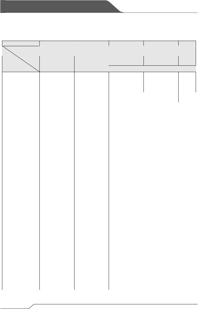

 XC6219/XC6211 Series
■ELECTRICAL CHARACTERISTICS (Continued)
●Voltage Chart
SYMBOL |
E-0 |
|
E-1 |
E-2 |
E-3 |
PARAMETER |
|
|
DROPOUT |
DROPOUT |
Power |
|
OUTPUT VOLTAGE |
OUTPUT VOLTAGE |
Supply |
||
|
VOLTAGE1 (mV) |
VOLTAGE2 (mV) |
|||
|
(2%) |
(1%) |
Rejection |
||
|
(IOUT=30mA) |
(IOUT=100mA) |
|||
|
(V) |
(V) |
Ratio |
||
|
|
|
|||
OUTPUT VOLTAGE |
|
|
Ta=25 |
Ta=25 |
Ta=25 |
|
VOUT(T) |
|
|
|
VOUT |
|
VOUT |
|
|
|
|
Vdif1 |
|
Vdif2 |
|
|
|
|
PSRR |
|
|||||||||||
|
|
|
MIN |
|
|
MAX |
|
|
MIN |
|
|
MAX |
|
|
TYP |
|
|
MAX |
|
|
TYP |
|
|
MAX |
|
|
|
TYP |
|
|
|
|
|
|
|
|
|
|
|
|
|
|
|
|
|
|
|
|
|
|
|
|
|
|
|||||||||
3.00 |
|
2.940 |
|
3.060 |
|
2.970 |
|
|
3.030 |
|
|
|
|
|
|
|
|
|
|
|
270 |
|
|
|
|
|
|
||||
3.05 |
|
2.989 |
|
3.111 |
|
3.020 |
|
|
3.081 |
|
|
|
|
|
|
|
|
|
|
|
|
|
|
|
|
|
|||||
|
|
|
|
|
|
|
|
|
|
|
|
|
|
|
|
|
|
|
|
|
|
|
|||||||||
3.10 |
|
3.038 |
|
3.162 |
|
3.069 |
|
|
3.131 |
|
|
|
|
|
|
|
|
|
|
|
|
|
|
|
|
|
|
||||
3.15 |
|
3.087 |
|
3.213 |
|
3.119 |
|
|
3.182 |
|
|
|
|
|
|
|
|
|
|
|
|
|
|
|
|
|
|
||||
|
|
|
|
|
|
|
|
|
|
|
|
|
|
|
|
|
|
|
|
|
|
|
|
|
|
|
|
||||
3.20 |
|
3.136 |
|
3.264 |
|
3.168 |
|
|
3.232 |
|
|
|
|
|
|
|
|
|
|
|
|
|
|
|
|
|
|
||||
3.25 |
|
3.185 |
|
3.315 |
|
3.218 |
|
|
3.283 |
|
|
|
|
|
|
|
|
|
|
|
|
|
|
|
|
|
|
||||
3.30 |
|
3.234 |
|
3.366 |
|
3.267 |
|
|
3.333 |
|
|
|
|
|
|
|
|
|
|
|
|
|
|
|
|
|
|
||||
3.35 |
|
3.283 |
|
3.417 |
|
3.317 |
|
|
3.384 |
|
|
|
|
|
|
|
|
|
|
|
|
|
|
|
|
|
|
||||
3.40 |
|
3.332 |
|
3.468 |
|
3.366 |
|
|
3.434 |
|
|
|
|
|
|
|
|
|
|
|
|
|
|
|
|
|
|
||||
3.45 |
|
3.381 |
|
3.519 |
|
3.416 |
|
|
3.485 |
|
|
|
|
90 |
|
200 |
|
|
|
|
|
|
|
|
|
||||||
3.50 |
|
3.430 |
|
3.570 |
|
3.465 |
|
|
3.535 |
|
|
|
|
|
|
|
250 |
|
|
|
|
|
|
||||||||
|
|
|
|
|
|
|
|
|
|
|
|
|
|
|
|
|
|
|
|
|
|
||||||||||
3.55 |
|
3.479 |
|
3.621 |
|
3.515 |
|
|
3.586 |
|
|
|
|
|
|
|
|
|
|
|
|
|
|
|
|
|
|||||
|
|
|
|
|
|
|
|
|
|
|
|
|
|
|
|
|
|
|
|
|
|
|
|||||||||
3.60 |
|
3.528 |
|
3.672 |
|
3.564 |
|
|
3.636 |
|
|
|
|
|
|
|
|
|
|
|
|
|
|
|
|
|
|
||||
3.65 |
|
3.577 |
|
3.723 |
|
3.614 |
|
|
3.687 |
|
|
|
|
|
|
|
|
|
|
|
|
|
|
|
|
|
|
||||
|
|
|
|
|
|
|
|
|
|
|
|
|
|
|
|
|
|
|
|
|
|
|
|
|
|
|
|
||||
3.70 |
|
3.626 |
|
3.774 |
|
3.663 |
|
|
3.737 |
|
|
|
|
|
|
|
|
|
|
|
|
|
|
|
|
|
|
||||
3.75 |
|
3.675 |
|
3.825 |
|
3.713 |
|
|
3.788 |
|
|
|
|
|
|
|
|
|
|
|
|
|
|
|
|
|
|
||||
3.80 |
|
3.724 |
|
3.876 |
|
3.762 |
|
|
3.838 |
|
|
|
|
|
|
|
|
|
|
|
|
|
|
|
|
|
|
||||
3.85 |
|
3.773 |
|
3.927 |
|
3.812 |
|
|
3.889 |
|
|
|
|
|
|
|
|
|
|
|
|
|
|
|
|
|
|
||||
3.90 |
|
3.822 |
|
3.978 |
|
3.861 |
|
|
3.939 |
|
|
|
|
|
|
|
|
|
|
|
|
|
|
|
|
|
|
||||
3.95 |
|
3.871 |
|
4.029 |
|
3.911 |
|
|
3.990 |
|
60 |
|
|
|
|
|
|
|
|
|
|
|
|
|
|
|
|||||
4.00 |
|
3.920 |
|
4.080 |
|
3.960 |
|
|
4.040 |
|
|
|
|
|
|
|
|
|
|
|
70 |
|
|
||||||||
|
|
|
|
|
|
|
|
|
|
|
|
|
|
|
|
|
|
|
|
||||||||||||
4.05 |
|
3.969 |
|
4.131 |
|
4.010 |
|
|
4.091 |
|
|
|
|
|
|
|
|
|
|
|
|
|
|
|
|
|
|
||||
4.10 |
|
4.018 |
|
4.182 |
|
4.059 |
|
|
4.141 |
|
|
|
|
|
|
|
|
|
|
|
|
|
|
|
|
|
|
||||
4.15 |
|
4.067 |
|
4.233 |
|
4.109 |
|
|
4.192 |
|
|
|
|
|
|
|
|
|
|
|
|
|
|
|
|
|
|
||||
|
|
|
|
|
|
|
|
|
|
|
|
|
|
|
|
|
|
|
|
|
|
|
|
|
|
|
|
||||
4.20 |
|
4.116 |
|
4.284 |
|
4.158 |
|
|
4.242 |
|
|
|
|
|
|
|
|
|
|
|
|
|
|
|
|
|
|
||||
4.25 |
|
4.165 |
|
4.335 |
|
4.208 |
|
|
4.293 |
|
|
|
|
|
|
|
|
|
|
|
|
|
|
|
|
|
|
||||
4.30 |
|
4.214 |
|
4.386 |
|
4.257 |
|
|
4.343 |
|
|
|
|
|
|
|
|
|
|
|
|
|
|
|
|
|
|
||||
4.35 |
|
4.263 |
|
4.437 |
|
4.307 |
|
|
4.394 |
|
|
|
|
|
|
|
|
|
|
|
|
|
|
|
|
|
|
||||
4.40 |
|
4.312 |
|
4.488 |
|
4.356 |
|
|
4.444 |
|
|
|
|
|
|
|
|
|
|
|
|
|
|
|
|
|
|
||||
4.45 |
|
4.361 |
|
4.539 |
|
4.405 |
|
|
4.494 |
|
|
|
|
80 |
|
180 |
|
|
230 |
|
|
|
|
|
|
||||||
4.50 |
|
4.410 |
|
4.590 |
|
4.455 |
|
|
4.545 |
|
|
|
|
|
|
|
|
|
|
|
|
|
|||||||||
|
|
|
|
|
|
|
|
|
|
|
|
|
|
|
|
|
|
|
|
|
|
|
|||||||||
4.55 |
|
4.459 |
|
4.641 |
|
4.504 |
|
|
4.595 |
|
|
|
|
|
|
|
|
|
|
|
|
|
|
|
|
|
|
||||
4.60 |
|
4.508 |
|
4.692 |
|
4.554 |
|
|
4.646 |
|
|
|
|
|
|
|
|
|
|
|
|
|
|
|
|
|
|
||||
4.65 |
|
4.557 |
|
4.743 |
|
4.603 |
|
|
4.696 |
|
|
|
|
|
|
|
|
|
|
|
|
|
|
|
|
|
|
||||
4.70 |
|
4.606 |
|
4.794 |
|
4.653 |
|
|
4.747 |
|
|
|
|
|
|
|
|
|
|
|
|
|
|
|
|
|
|
||||
4.75 |
|
4.655 |
|
4.845 |
|
4.702 |
|
|
4.797 |
|
|
|
|
|
|
|
|
|
|
|
|
|
|
|
|
|
|
||||
4.80 |
|
4.704 |
|
4.896 |
|
4.752 |
|
|
4.848 |
|
|
|
|
|
|
|
|
|
|
|
|
|
|
|
|
|
|
||||
4.85 |
|
4.753 |
|
4.947 |
|
4.801 |
|
|
4.898 |
|
|
|
|
|
|
|
|
|
|
|
|
|
|
|
|
|
|
||||
4.90 |
|
4.802 |
|
4.998 |
|
4.851 |
|
|
4.949 |
|
|
|
|
|
|
|
|
|
|
|
|
|
|
|
|
|
|
||||
4.95 |
|
4.851 |
|
5.049 |
|
4.900 |
|
|
4.999 |
|
|
|
|
|
|
|
|
|
|
|
|
|
|
|
|
|
|
||||
5.00 |
|
4.900 |
|
5.100 |
|
4.950 |
|
|
5.050 |
|
50 |
|
70 |
|
160 |
|
|
210 |
|
|
|
|
|
|
|||||||
10/30
 Loading...