

X
XC6219 Series
High Speed LDO Regulators, Low ESR Cap. Compatible, ON/OFF Switch
October 4, 2004 V5
CMOS Low Power Consumption APPLICATIONS
Dropout Voltage 60mV @ 30mA Mobile phones
200mV @ 100mA
Output Current 150mA (VOUT<1.75V)
240mA (VOUT>
1.8V) Cameras, video cameras
(300mA limit)
Highly Accurate +
2% Battery powered equipment
(+
30mV when VOUT>1.5V)
Cordless phones and radio communication equipment
Portable games
Reference voltage sources
Output Voltage Range 0.9V to 5.0V (50mV increments)
Low ESR Ceramic Capacitor Compatible
GENERAL DESCRIPTION FEATURES
The XC6219 series are highly accurate, low noise, CMOS LDO Maximum Output Current 150mA (VOUT<1.75V)
Voltage Regulators. Offering low output noise, high ripple rejection 240mA (VOUT>
ratio, low dropout and very fast turn-on times, the XC6219 series (300mA limit (TYP))
is ideal for today’s cutting edge mobile phone. Dropout Voltage 200mV (IOUT=100mA)
Internally the XC6219 includes a reference voltage source, error Operating Voltage Range 2.0V ~ 6.0V
amplifiers, driver transistors, current limiters and phase Output Voltage Range 0.9V ~ 5.0V (50mV steps)
compensators. The XC6219’s current limiters' foldback circuit Highly Accurate +
also operates as a short protect for the output current limiter and. +
the output pin. The output voltage is set by laser trimming. Low Power Consumption 25µA (TYP.)
Voltages are selectable in 50mV steps within a range of Standby Current Less than 0.1µA (TYP.)
0.9V to 5.0V. The XC6219 series is also fully compatible with low High Ripple Rejection 65dB (10kHz)
ESR ceramic capacitors, reducing cost and improving output stability. Operating Temperature Range - 40
This high level of output stability is maintained even during frequent Low ESR Ceramic Compatible Ceramic Capacitor
load fluctuations, due to the excellent transient response performance Ultra Small Packages SOT-25 (SOT-23-5)
and high PSRR achieved across a broad range of frequencies. SOT-89
The CE function allows the output of regulator to be turned off, USP-6B
resulting in greatly reduced power consumption.
The XC6219 series is available in the SOT-25 (SOT-23-5), SOT-89
or USP-6B ‘chip-scale’ package. Measuring only 2.0mm x 1.8mm
the USP-6B is perfect for applications where PCB area is critical.
2% (VOUT>1.5V)
30mV (VOUT<1.5V)
O
C to 85OC
1.8V)
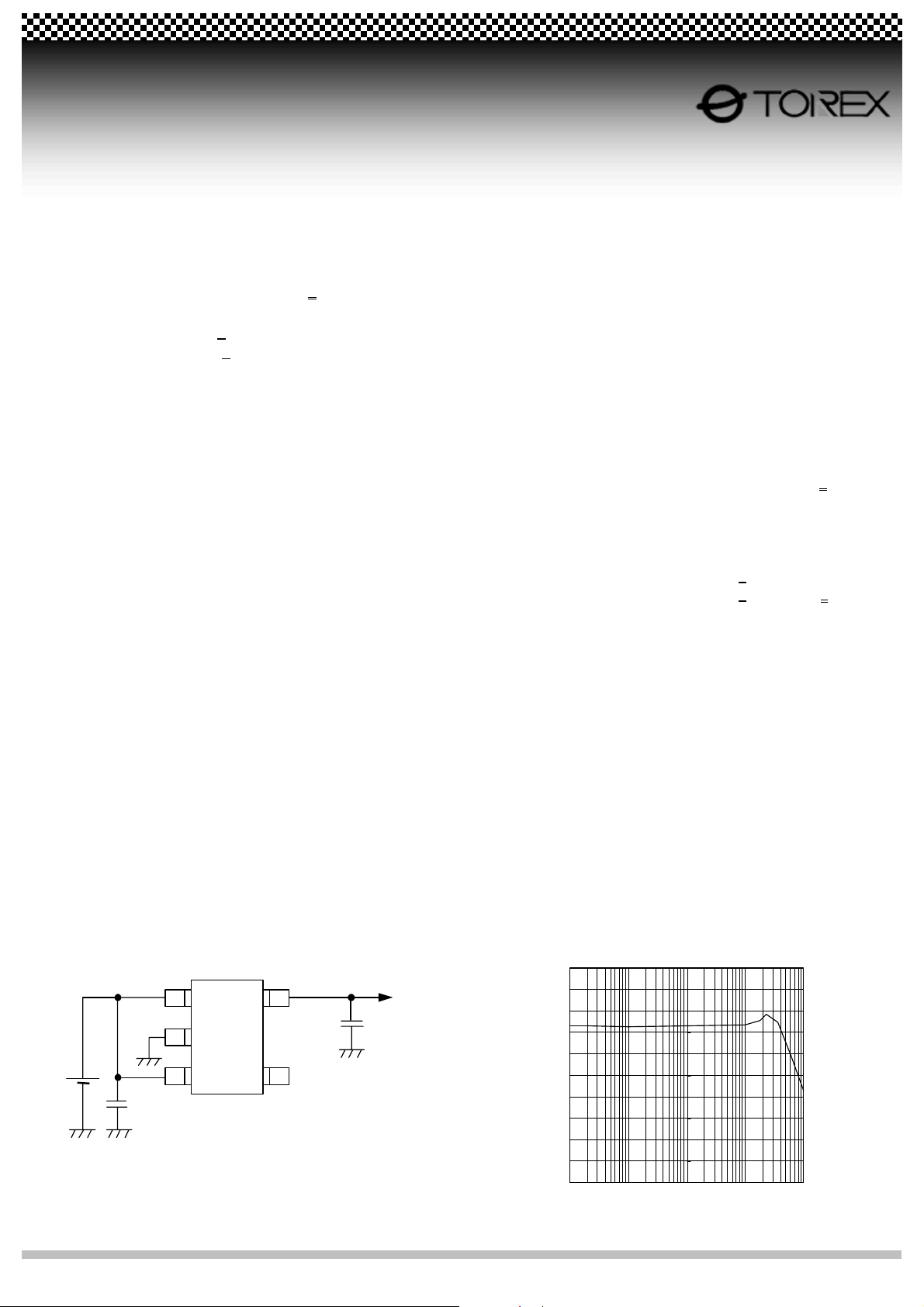
TYPICAL APPLICATION CIRCUIT TYPICAL PERFORMANCE CHARACTERISTICS
Ripple Rejection Rate
1
2
3 4
CIN
1µF
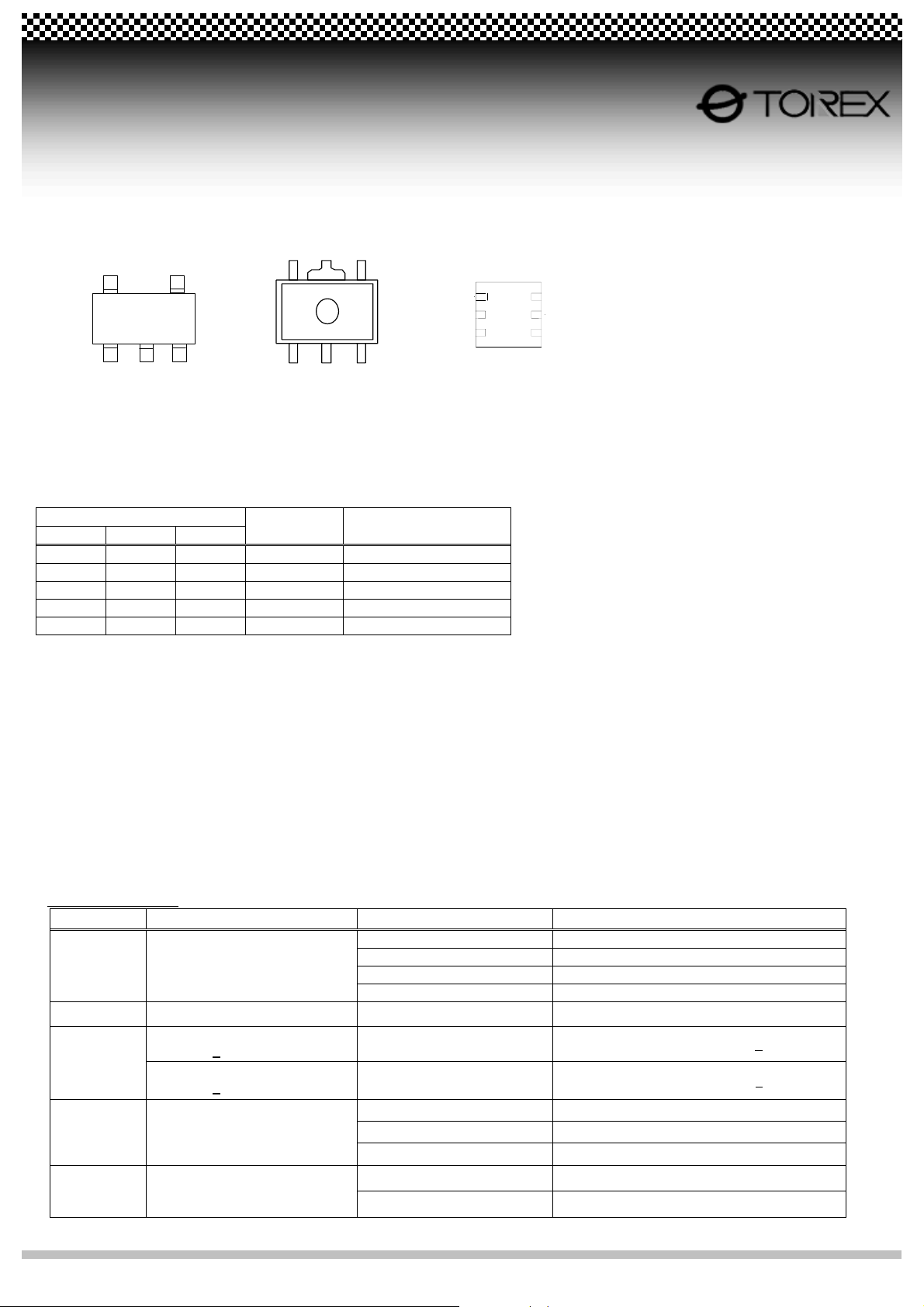
SOT-25 (SOT-23-5)
VOUT
VIN
VSS
CE NC
5
CL
1µF
100
90
80
70
60
50
40
30
20
Ripple Rejec tion Rat e RR (dB)
10
0
0.01 0.1 1 10 100
C6219x302
VIN=3.0V, DC+1Vp-pAC
IOUT=50mA , CL=1uF (ceramics )
Ripple Frequency f (kHz )
Data Sheet 1 R000026
XC6219 Series
High Speed LDO Regulators, Low ESR Cap. Compatible, ON/OFF Switch
PIN CONFIGURATION
V
OUT
5
(NC)
4
VOU T5VSS
13
2
V
IN
V
SS
CE
SOT-25 (SOT-23-5) SOT-89-5 USP-6B
(TOP VIEW) (TOP VIEW) (BOTTOM VIEW)
1
NC
2
VSS
VIN
4
2
6
CE
VSS
5
4
NC
*Please use the circuit without connecting to the heat dissipation pad.
If the pad needs to be connected to other pins, it should be
noted that the pin configuration of the USP-6B package is
different depending on the IC series.
CE
1
VIN
2
NC
VOUT
3
3
PIN ASSIGNMENT
PIN NUMBER
SOT-25 SOT-89-5 USP-6B
PIN NAME FUNCTIONS
1 4 1 VIN Power Input
2 2 5 VSS Ground
3 3 6 CE ON / OFF Control
4 1 2, 4 NC No Connection
5 5 3 VOUT Output
PRODUCT CLASSIFICATION
Selection Guide
The following options for the CE pin logic and internal pull-up/down are available:
High Active + no pull-down resistor built-in (standard)
High Active + 2.0MΩ pull-down resistor built-in <between CE-VSS> (semi-custom)
Low Active + no pull-up resistor built-in (semi-custom)
Low Active + 2.0MΩ pull-up resistor built-in <between VIN-CE> (semi-custom)
Note: *With the pull-up resistor or pull-down resistor built-in types, the supply current during operation will increase by VIN / 2.0MΩ (TYP.)
Ordering Information
XC6219
123456
DESIGNATOR DESCRIPTION SYMBOL DESCRIPTION
A : High Active (ull-down resistor built in)
1
2 3
4
5
6
CE Pin Logic
Output Voltage 09 ~ 50
Output Voltage, 100mV increments,
2% accuracy
+
Output Voltage, 50mV increments,
2% accuracy
+
Packages
Taping Direction
B : High Active (no pull-down resistor built in)
C : Low Active (pull-up resistor built in)
D : Low Active (no pull-up resistor built in)
: e.g.
2=3, 3=0, D 3.0V
2
A
: e.g.
2=2, 3=8, 4=2 D 2.80V, +2%
: e.g.
2=2, 3=8, 4=A D 2.85V, +2%
M : SOT-25 (SOT-23-5)
P : SOT-89-5
D : USP-6B
R : Embossed tape, Standard feed
L : Embossed tape, Reverse feed
Data Sheet 2 R000026
XC6219 Series
High Speed LDO Regulators, Low ESR Cap. Compatible, ON/OFF Switch
PACKAGING INFORMATION
SOT-25 (SOT-23-5)
SOT-89-5
USP-6B
2.0 + 0.15
0.5+0.1(0.45)
(0.05)
O
5
A'A
1
O
( 0.45)
2
3
1.8 + 0.15
(0.45) (0.45)
O
4
5
(0.125)
-0.05
+0.15
0.65
3
0.2+0.05
2
1
0.2+0.05
0.25+0.1
AAA
2
0.7 + 0.03
2
1.0+0.1
AA
4
0.25+0.1
6
5
4
O
5
0.005+0.00
4
5
6
2 2
(0.27)(0.27)(0.27)
2
0.5+0.1
0.5+0.1
0.1+0.03 0.1+0.03
4
O
5
4
-0.005
+0.01
A - A' cross-section
drawing
* Pin no. 1 is thicker than other pins
0.05
Data Sheet 3 R000026
XC6219 Series
High Speed LDO Regulators, Low ESR Cap. Compatible, ON/OFF Switch
MARKING RULE
SOT-25 (SOT-23-5)
1 Represents product series
MARK PRODUCT SERIES
L XC6219xxxxMx
SOT-25 (TOP VIEW)
2 Represents type of regulator
MARK
VOUT 100mV STEPS VOUT 50mV STEPS
VOUT:0.1~3.0V VOUT:3.1~6.0V VOUT:0.15~3.05V VOUT:3.15~6.05V
V A E L XC6219AxxxMx
X B F M XC6219BxxxMx
Y C H N XC6219CxxxMx
Z D K P XC6219DxxxMx
3 Represents output voltage
MARK OUTPUT VOLTAGE MARK OUTPUT VOLTAGE
0 - 3.1 - 3.15 F 1.6 4.6 1.65 4.65
1 - 3.2 - 3.25 H 1.7 4.7 1.75 4.75
2 - 3.3 - 3.35 K 1.8 4.8 1.85 4.85
3 - 3.4 - 3.45 L 1.9 4.9 1.95 4.95
4 - 3.5 - 3.55 M 2.0 5.0 2.05
5 - 3.6 - 3.65 N 2.1 2.15
6 - 3.7 - 3.75 P 2.2 2.25
7 - 3.8 - 3.85 R 2.3 2.35
8 0.9 3.9 0.95 3.95 S 2.4 2.45
9 1.0 4.0 1.05 4.05 T 2.5 2.55
A 1.1 4.1 1.15 4.15 U 2.6 2.65
B 1.2 4.2 1.25 4.25 V 2.7 2.75
C 1.3 4.3 1.35 4.35 X 2.8 2.85
D 1.4 4.4 1.45 4.45 Y 2.9 2.95
E 1.5 4.5 1.55 4.55 Z 3.0 3.05
4 Represents production lot number
0 to 9, A to Z, reverse character of 0 to 9, A to Z repeated. (G, I, J, O, Q, W excepted)
PRODUCT SERIES
1234
Data Sheet 4 R000026
XC6219 Series
High Speed LDO Regulators, Low ESR Cap. Compatible, ON/OFF Switch
MARKING RULE (Continued)
USP-6B
1 2 Represents product series
MARK
1 2
L XC6219xxxxDx
USP-6B (TOP VIEW)
3 Represents type of regulator
MAKR TYPE PRODUCT SERIES
A High Active, Pull-down resistor built-in (semi-custom) XC6219AxxxMx
B High Active, Pull-down resistor built-in (semi-custom) XC6219BxxxMx
C Low Active, Pull-up resistor built-in (semi-custom) XC6219CxxxMx
D Low Active, Pull-up resistor built-in (semi-custom) XC6219DxxxMx
4 Represents product series
MARK VOLTAGE PRODUCT SERIES
3 3.X XC6219x3xxDx
5 5.X XC6219x5xxDx
3 Represents output voltage
MARK VOLTAGE PRODUCT SERIES MARK VOLTAGE PRODUCT SERIES
0 X.0 XC6219xx0xDx A X.05 XC6219xx0ADx
1 X.1 XC6219xx1xDx B X.15 XC6219xx1ADx
2 X.2 XC6219xx2xDx C X.25 XC6219xx2ADx
3 X.3 XC6219xx3xDx D X.35 XC6219xx3ADx
4 X.4 XC6219xx4xDx E X.45 XC6219xx4ADx
5 X.5 XC6219xx5xDx F X.55 XC6219xx5ADx
6 X.6 XC6219xx6xDx H X.65 XC6219xx6ADx
7 X.7 XC6219xx7xDx K X.75 XC6219xx7ADx
8 X.8 XC6219xx8xDx L X.85 XC6219xx8ADx
9 X.9 XC6219xx9xDx M X.95 XC6219xx9ADx
4 Represents production lot number
0 to 9, A to Z repeated. (G, I, J, O, Q, W excepted)
* No character inversion used.
PRODUCT SERIES
1
2
3
4
56
1
23
6
5
4
Data Sheet 5 R000026
XC6219 Series
High Speed LDO Regulators, Low ESR Cap. Compatible, ON/OFF Switch
BLOCK DIAGRAM
CE
ON/OFF
Control
each circuit
IN
V
Current
Limit
V
OUT
R2
Voltage
Reference
R1
SS
V
ABSOLUTE MAXIMUM RATINGS
Ta =2 5OC
PARAMETER SYMBOL RATINGS UNITS
Input Voltage VIN 7.0 V
Output Current IOUT 500 mA
Output Voltage VOUT VSS – 0.3 ~ VIN + 0.3 V
CE Pin Voltage VCE VSS – 0.3 ~ VIN + 0.3 V
SOT-25 250
Power Dissipation
SOT-89 500
USP-6B
Operating Temperature Range Topr - 40 ~ + 85
Storage Temperature Range Tstg - 55 ~ + 125
Pd
100
mW
O
C
O
C
Data Sheet 6 R000026

XC6219 Series
High Speed LDO Regulators, Low ESR Cap. Compatible, ON/OFF Switch
ELECTRICAL CHARACTERISTICS
XC6219B series
Ta =2 5
PARAMETER SYMBOL CONDITIONS MAX. TYP. MIN. UNITS CIRCUIT
Output Voltage VOUT(E) IOUT=30mA x 0.98 VOUT(T) x 1.02 V
Maximum Output Current IOUTMAX 150 - - mA
Load Regulation UVOUT 1mA<IOUT<100mA - 15 50 mV
Dropout Voltage
Supply Current IDD VCE=VIN - 25 50
Standby Current Istby VCE=VSS - 0.01 0.10
Line Regulation
Input Voltage VIN 2.0 6.0 V -
Output Voltage Temperature UVOUT/ IOUT=30mA
Characteristics UTo pr VOUT -40OC<Topr<85OC
Ripple Rejection Rate PSRR IOUT=50mA, f=10kHz - 65 - dB
Current Limiter Ilim - 300 - mA
Short Circuit Current Ishort - 50 - mA
EN ‘High’ Voltage VCEH 1.60 VIN V
EN ‘Low’ Voltage VCEL 0.25 V
EN ‘High’ Current ICEH VCE=VIN -0.10 0.10
EN ‘Low’ Current ICEL VCE=VSS -0.10 0.10
NOTE:
*1: VOUT(T) = Specified output voltage
*2: VOUT(E) = Effective output voltage (I.e. the output voltage when "VOUT(T)+1.0V" is provided at the VIN pin while maintaining a certain IOUT value.)
3: Vdif={VIN1
*4: VOUT=A voltage equal to 98% of the output voltage whenever an amply stabilized IOUT {VOUT(T)+1.0V} is input.
*5: VIN=The Input Voltage when VOUT appears as Input Voltage is gradually decreased.
*6: Unless otherwise stated, VIN=VOUT(T)+1.0V.
(*5)-
VOUT1
(*4)
}
Vdif1 IOUT=30mA E-1 mV
Vdif2 IOUT=100mA E-2 mV
µA
µA
UVOUT/ VOUT(T)+1.0V<VIN<7.0V
VOUT IOUT=30mA
UVIN
- 0.01 0.20 %/V
- 100 - ppm/
µA
µA
O
C
DROPOUT VOLTAGE CHART
SYMBOL
PARAMETER
OUTPUT VOLTAGE
0.9 1100 1100 1110 1100 1150 1200
1.50 500 500 510 500
1.80 ~ 1.85 200 200 210 200 300 400
1.90 ~ 1.95 100 120 150 100 280 380
2.00 ~ 2.05 - 80 120 - 240 350
2.10 ~ 2.25 - 80 120 - 240 330
2.30 ~ 2.45 - 80 120 - 240 310
2.50 ~ 2.75 - 70 100 - 220 290
2.80 ~ 2.95 - 70 100 - 220 270
3.00 ~ 3.05 - 60 90 - 200 270
3.10 ~ 3.95 - 60 90 - 200 250
4.00 ~ 4.95 - 60 80 - 180 230
5.00 - 50 70 - 160 210
* The input voltage 2.0V (MIN) is needed to operate the series.
When the output voltage is less than 2.0V, 2.0V-VOUT(T) of dropout voltage is needed at minimum.
MIN. TYP. MAX. MIN. TYP. MAX.
E-1 E-2
Vdif1 Vdif2
550
600
1
1
1
1
2
2
1
1
4
1
1
1
2
2
2
O
C
Data Sheet 7 R000026

XC6219 Series
High Speed LDO Regulators, Low ESR Cap. Compatible, ON/OFF Switch
TEST CIRCUITS
Circuit 1
VIN VOUT
V
CIN=1.0µF
(ceramic)
CE
VSS
V
CL=1.0µF
(cerami c)
V
Circuit 2
Circuit
A
A
3
VIN VOUT
CE
VSS
OPEN
VIN VOUT
CIN=1.0µF
(ceramic )
CE
VSS
CL=1.0µF
(ceramic )
IOUT=10mA
Circuit 4
VIN={VOUT+1}V
+0.5V
p-pAC
DC
V
VIN VOUT
CE
VSS
CL=1.0µF
(ceramic)
V
A
RL
F.F.T
IOUT=50mA
Data Sheet 8 R000026

XC6219 Series
High Speed LDO Regulators, Low ESR Cap. Compatible, ON/OFF Switch
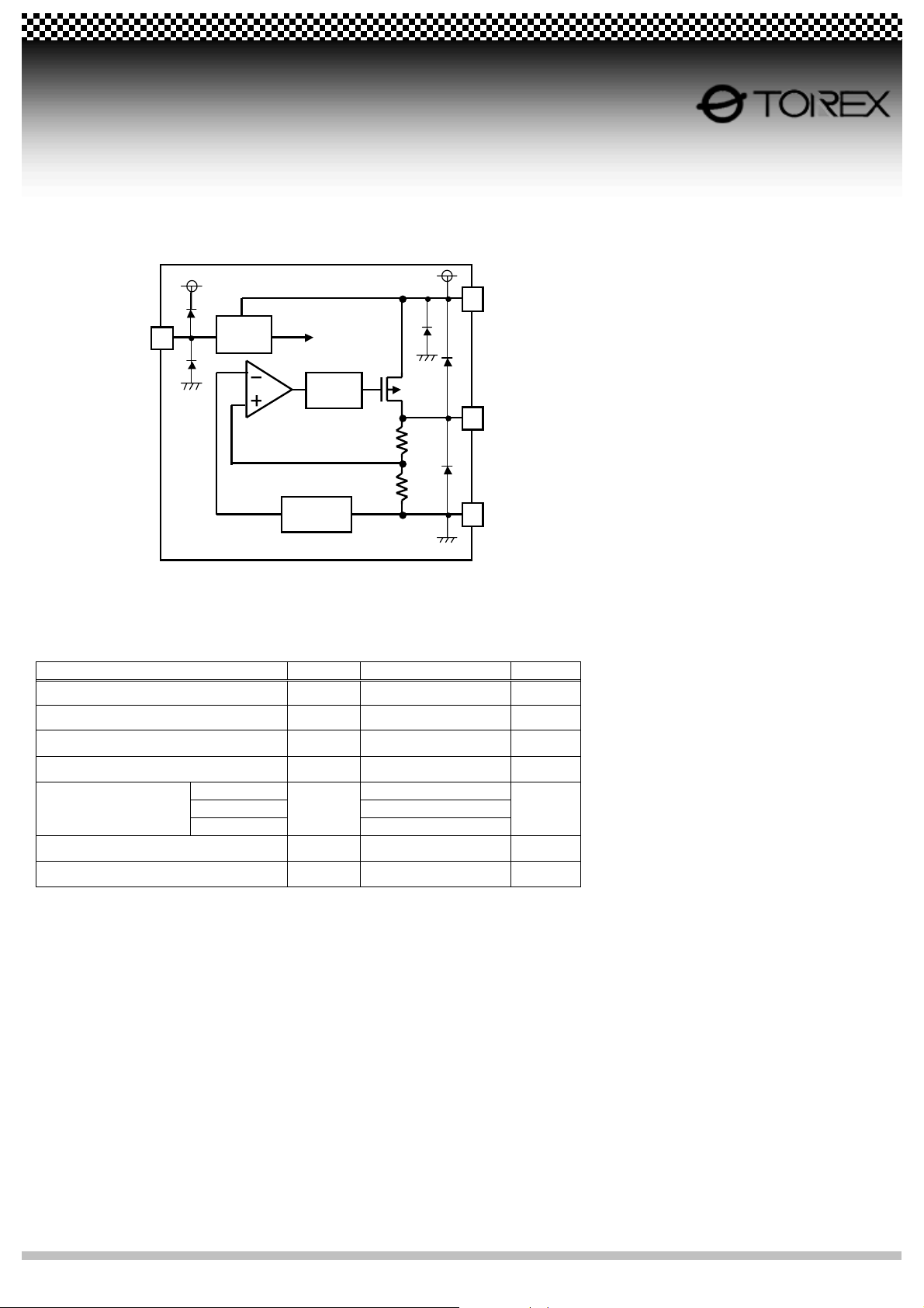
OPERATIONAL EXPLANATION
<Output Voltage Control>
The voltage divided by resistors R1 & R2 is compared with the internal reference voltage by the error amplifier. The P-channel MOSFET, which is connected
to the VOUT pin, is then driven by the subsequent output signal. The output voltage at the VOUT pin is controlled and stabilized by a system of negative
feedback. The current limit circuit and short protect circuit operate in relation to the level of output current. Further, the IC's internal circuitry can be shutdown
via the CE pin's signal.
<Low ESR Capacitors>
With the XC6219 series, a stable output voltage is achievable even if used with low ESR capacitors as a phase compensation circuit is built-in. In order to
ensure the effectiveness of the phase compensation, we suggest that an output capacitor (CL) is connected as close as possible to the output pin (VOUT)
and the VSS pin. Please use an output capacitor with a capacitance value of at least 1µF. Also, please connect an input capacitor (CIN) of 0.1µF between the
VIN pin and the VSS pin in order to ensure a stable power input.
<Current Limiter, Short-Circuit Protection>
The XC6219 series includes a combination of a fixed current limiter circuit & a foldback circuit, which aid the operations of the current limiter and circuit
protection. When the load current reaches the current limit level, the fixed current limiter circuit operates and output voltage drops. As a result of this drop in
output voltage, the foldback circuit operates, output voltage drops further and output current decreases. When the output pin is shorted, a current of about
50mA flows.
<CE Pin>
The IC's internal circuitry can be shutdown via the signal from the CE pin with the XC6219 series. In shutdown mode, output at the VOUT pin will be pulled
down to the VSS level via R1 & R2. The operational logic of the IC's CE pin is selectable (please refer to the selection guide on page 2). Note that as the
standard XC6219B type's regulator 1 and 2 are both ' High Active/No Pull Down', operations will become unstable with the CE pin open. Although the CE pin is
equal to an inverter input with CMOS hysteresis, with either the pull-up or pull-down options, the CE pin input current will increase when the IC is in operation.
We suggest that you use this IC with either a VIN voltage or a VSS voltage input at the CE pin. If this IC is used with the correct specifications for the CE pin,
the operational logic is fixed and the IC will operate normally. However, supply current may increase as a result of through current in the IC's internal circuitry.
CE
ON/OFF
Control
each circuit
Current
Limit
R2
R1
Voltage
Reference
V
V
V
IN
OUT
SS
NOTES ON USE
1. Please use this IC within the stated absolute maximum ratings. The IC is liable to malfunction should the ratings be exceeded.
2. Where wiring impedance is high, operations may become unstable due to noise and/or phase lag depending on output current. Please keep the resistance
low between VIN and VSS wiring in particular.
3. Please wire the input capacitor (CIN) and the output capacitor (CL) as close to the IC as possible.
Data Sheet 9 R000026

XC6219 Series
High Speed LDO Regulators, Low ESR Cap. Compatible, ON/OFF Switch
ELECTRICAL CHARACTERISTICS
(1) Output Voltage vs. Output Current
2.0
1.5
1.0
0.5
Output Volt age VOUT (V)
0.0
0 50 100 150 200 250 300 350 400
3.0
2.5
2.0
1.5
1.0
0.5
Output Volt age VOUT (V)
0.0
0 50 100 150 200 250 300 350 400
4.0
3.5
3.0
2.5
2.0
1.5
1.0
Output Volt age VOUT (V)
0.5
0.0
0 50 100 150 200 250 300 350 400
XC6219x182
VIN=2.8V
CIN=1uF (ceramics ), CL= 1uF (ceramics)
25
- 40
O
O
O
Topr= 85
Output Current IOUT (mA)
XC6219x252
VIN=3.5V
CIN=1uF (ceramics ), CL= 1uF (ceramics)
Output Current IOUT (mA)
XC6219x302
VIN=4.0V
CIN=1uF (ceramics ), CL= 1uF (ceramics)
Topr= 85OC
Output Current IOUT (mA)
25
- 40
O
O
2.0
1.5
1.0
C
C
C
C
C
0.5
Output Volt age VOUT (V)
0.0
0 50 100 150 200 250 300 350 400
3.0
2.5
2.0
1.5
1.0
0.5
Output Volt age VOUT (V)
0.0
0 50 100 150 200 250 300 350 400
4.0
3.5
3.0
2.5
2.0
1.5
1.0
Output Volt age VOUT (V)
0.5
0.0
0 50 100 150 200 250 300 350 400
CIN=1uF (ceramics ), CL= 1uF (ceramics)
VIN=4.8V
Output Current IOUT (mA)
CIN=1uF (ceramics ), CL= 1uF (ceramics)
VIN=5.5V
Output Current IOUT (mA)
CIN=1uF (ceramics ), CL= 1uF (ceramics)
VIN=5V
VIN=6V
Output Current IOUT (mA)
XC6219x182
VIN=2.8V
VIN=3.8V
VIN=2.1V
XC6219x252
VIN=4.5V
VIN=3.5V
VIN=2.8V
XC6219x302
VIN=4V
VIN=3.3V
Data Sheet 10 R000026

XC6219 Series
High Speed LDO Regulators, Low ESR Cap. Compatible, ON/OFF Switch
ELECTRICAL CHARACTERISTICS (Continued)
(2) Output Voltage vs. Input Voltage
2.0
1.8
1.6
1.4
1.2
Output Volt age VOUT (V)
1.0
1.3 1.8 2.3
2.7
2.5
2.3
2.1
1.9
Output Volt age VOUT (V)
1.7
22.53
3.2
3.0
2.8
2.6
2.4
Output Volt age VOUT (V)
2.2
2.5 3 3.5
XC6219x182
Topr=25OC
CIN=1uF (ceramics ), CL= 1uF (ceramics)
IOUT=0mA
1mA
30mA
100mA
Input Voltage VIN (V)
XC6219x252
CIN=1uF (ceramics ), CL= 1uF (ceramics)
Input Voltage VIN (V)
Topr=25OC
IOUT=0mA
1mA
30mA
100mA
XC6219x302
Topr=25OC
CIN=1uF (ceramics ), CL= 1uF (ceramics)
IOUT=0mA
1mA
30mA
100mA
Input Voltage VIN (V)
1.90
1.85
1.80
1.75
1.70
Output Volt age VOUT (V)
1.65
3.0 4.0 5.0 6.0
2.60
2.55
2.50
2.45
2.40
Output Volt age VOUT (V)
2.35
3.0 3.5 4.0 4. 5 5.0 5.5 6.0
3.10
3.05
3.00
2.95
2.90
Output Volt age VOUT (V)
2.85
4.0 4.5 5.0 5.5 6. 0
CIN=1uF (ceramics ), CL= 1uF (ceramics)
CIN=1uF (ceramics ), CL= 1uF (ceramics)
CIN=1uF (ceramics ), CL= 1uF (ceramics)
XC6219x182
Topr=25OC
IOUT=0mA
1mA
30mA
Input Voltage VIN (V)
XC6219x252
Topr=25OC
IOUT=0mA
1mA
30mA
Input Voltage VIN (V)
XC6219x302
Topr=25OC
IOUT=0mA
1mA
30mA
Input Voltage VIN (V)
Data Sheet 11 R000026

XC6219 Series
High Speed LDO Regulators, Low ESR Cap. Compatible, ON/OFF Switch
ELECTRICAL CHARACTERISTICS (Continued)
(3) Dropout Voltage vs. Output Current
1.0
0.8
0.6
0.4
0.2
Dropout Voltage Vdif (V)
0.0
0 40 80 120 160 200
1.0
0.8
0.6
0.4
0.2
Dropout Voltage Vdif (V)
0.0
0 40 80 120 160 200
(4) Supply Current vs. Input Voltage
50.0
A)
µ
40.0
30.0
20.0
10.0
Supply Current ISS (
0.0
01234 56
XC6219x182
CIN=1uF (ceramics ), CL= 1uF (ceramics)
O
25
- 40
C
O
C
O
C
Topr= 85
Output Current IOUT (mA)
XC6219x302
CIN=1uF (ceramics ), CL= 1uF (ceramics)
O
25
- 40
C
O
C
O
C
Topr= 85
Output Current IOUT (mA)
XC6219x182
Topr= 85OC
- 40
Input Voltage VIN (V)
25
1.0
0.8
0.6
CIN=1uF (ceramics ), CL= 1uF (ceramics)
Topr= 85
- 40
0.4
0.2
Dropout Voltage Vdif (V)
0.0
0 40 80 120 160 200
Output Current IOUT (mA)
50.0
40.0
A)
µ
30.0
20.0
O
C
O
C
Supply Current ISS (
10.0
0.0
01234 56
XC6219x252
O
C
O
C
25
O
C
XC6219x252
Input Voltage VIN (V)
Topr= 85OC
O
25
O
- 40
C
C
Data Sheet 12 R000026

XC6219 Series
High Speed LDO Regulators, Low ESR Cap. Compatible, ON/OFF Switch
ELECTRICAL CHARACTERISTICS (Continued)
(4) Supply Current vs. Input Voltage (Continued)
50.0
40.0
A)
µ
30.0
20.0
10.0
Supply Current ISS (
0.0
01234 56
(5) Output Voltage vs. Ambient Temperature
1.90
CIN=1uF (ceramics ), CL= 1uF (ceramics)
1.85
1.80
1.75
1.70
Output Volt age VOUT (V)
1.65
1.60
-40 -20 0 20 40 60 80 100
3.10
3.05
CIN=1uF (ceramics ), CL= 1uF (ceramics)
3.00
2.95
2.90
Output Volt age VOUT (V)
2.85
2.80
-40 -20 0 20 40 60 80 100
XC6210x302
Topr= 85OC
Input Voltage VIN (V)
XC6219x182
IOUT=0mA
Ambient Temperature Topr (
XC6219x302
IOUT=0mA
Ambient Temperature Topr (
25
- 40
VIN=2.8V
1mA
30mA
100mA
O
C)
VIN=4.0V
1mA
30mA
100mA
O
C)
O
C
O
C
2.60
2.55
2.50
2.45
2.40
Output Volt age VOUT (V)
2.35
2.30
-40 -20 0 20 40 60 80 100
CIN=1uF (ceramics ), CL= 1uF (ceramics)
Ambient Temperature Topr (
XC6219x252
VIN=3.5V
IOUT=0mA
1mA
30mA
100mA
O
C)
Data Sheet 13 R000026

XC6219 Series
High Speed LDO Regulators, Low ESR Cap. Compatible, ON/OFF Switch
ELECTRICAL CHARACTERISTICS (Continued)
(6) Supply Current vs. Ambient Temperature
50.0
40.0
A)
µ
30.0
20.0
Supply Current ISS (
10.0
0.0
-40-20 0 20406080100
50.0
40.0
A)
µ
30.0
20.0
Supply Current ISS (
10.0
0.0
-40 -20 0 20 40 60 80 100
XC6219x182
Ambient Temperature Topr (
XC6219x302
Ambient Temperature Topr (
VIN=2.8V
O
C)
VIN=4.0V
O
C)
50.0
40.0
A)
µ
30.0
20.0
Supply Current ISS (
10.0
0.0
-40-20 0 20406080100
Ambient Temperature Topr (
XC6219x252
VIN=3.5V
O
C)
Data Sheet 14 R000026

XC6219 Series
High Speed LDO Regulators, Low ESR Cap. Compatible, ON/OFF Switch
ELECTRICAL CHARACTERISTICS (Continued)
(7) Input Transient Response
5
4
3
2
1
Input Volt age VI N (V)
0
-1
5
4
3
2
1
Input Volt age VI N (V)
0
-1
5
4
3
2
1
Input Volt age VI N (V)
0
-1
XC6219x182
tr = tf = 5use
CL=1uF (ceramic s), IOUT=1mA
Input Voltage
Output Volt age
Time (40usec/div)
XC6219x182
tr = tf = 5use
CL=1uF (ceramic s), IOUT=100mA
Input Voltage
Output Volt age
Time (40usec/div)
XC6219x252
tr = tf = 5use
CL=1uF (ceramic s), IOUT=10mA
Input Voltage
Output Volt age
Time (40usec/div)
1.88
1.86
1.84
1.82
1.80
1.78
1.76
1.88
1.86
1.84
1.82
1.80
1.78
1.76
2.58
2.56
2.54
2.52
2.50
2.48
2.46
5
4
3
2
1
Output Volt age VOUT (V)
Output Volt age VOUT (V)
Output Volt age VOUT (V)
Input Volt age VI N (V)
0
-1
5
4
3
2
1
Input Volt age VI N (V)
0
-1
5
4
3
2
1
Input Volt age VI N (V)
0
-1
XC6219x182
tr = tf = 5use
CL=1uF (ceramic s), IOUT=10mA
Input Voltage
Output Volt age
Time (40usec/div)
XC6219x252
tr = tf = 5use
CL=1uF (ceramic s), IOUT=1mA
Input Voltage
Output Volt age
Time (40usec/div)
XC6219x252
tr = tf = 5use
CL=1uF (ceramic s), IOUT=100mA
Input Voltage
Output Volt age
Time (40usec/div)
1.88
1.86
1.84
1.82
1.80
Output Volt age VOUT (V)
1.78
1.76
2.58
2.56
2.54
2.52
2.50
Output Volt age VOUT (V)
2.48
2.46
2.58
2.56
2.54
2.52
2.50
Output Volt age VOUT (V)
2.48
2.46
Data Sheet 15 R000026

X
XC6219x18
XC6219 Series
High Speed LDO Regulators, Low ESR Cap. Compatible, ON/OFF Switch
ELECTRICAL CHARACTERISTICS (Continued)
(7) Input Transient Response (Continued)
(8) Load Transient Response
6
5
4
3
2
Input Volt age VI N (V)
1
0
6
5
4
3
2
Input Volt age VI N (V)
1
0
2.0
1.9
1.8
1.7
1.6
Output Volt age VOUT (V)
1.5
1.4
CIN=1uF (ceramics ), CL= 1uF (ceramics)
50mA
10mA
XC6219x302
tr = tf = 5use
CL=1uF (ceramic s), IOUT=1mA
Input Voltage
Output Volt age
Time (40usec/div)
XC6219x302
tr = tf = 5use
CL=1uF (ceramic s), IOUT=100mA
Input Voltage
Output Volt age
Time (40usec/div)
XC6219x182
VIN=2.8V, tr = tf = 5use
Output Volt age
Output Current
Time (40usec/div)
3.08
3.06
3.04
3.02
3.00
2.98
2.96
3.08
3.06
3.04
3.02
3.00
2.98
2.96
300
250
200
150
100
50
0
6
5
4
3
2
Output Volt age VOUT (V)
Output Volt age VOUT (V)
Output Current IOUT (mA)
Input Volt age VI N (V)
1
0
2.0
1.9
1.8
1.7
1.6
Output Volt age VOUT (V)
1.5
1.4
CIN=1uF (ceramics ), CL= 1uF (ceramics)
100mA
50mA
C6219x302
CL=1uF (ceramic s), IOUT=10mA
Input Voltage
Output Volt age
Time (40usec/div)
Output Volt age
Time (40usec/div)
tr = tf = 5use
2
VIN=2.8V, tr = tf = 5use
Output Current
3.08
3.06
3.04
3.02
3.00
2.98
2.96
300
250
200
150
100
50
0
Output Volt age VOUT (V)
Output Current IOUT (mA)
Data Sheet 16 R000026

X
XC6219x25
XC6219x30
XC6219 Series
High Speed LDO Regulators, Low ESR Cap. Compatible, ON/OFF Switch
ELECTRICAL CHARACTERISTICS (Continued)
(8) Load Transient Response (Continued)
2.0
1.9
1.8
1.7
1.6
Output Volt age VOUT (V)
1.5
1.4
2.7
2.6
2.5
2.4
2.3
Output Volt age VOUT (V)
2.2
2.1
3.2
3.1
3.0
2.9
2.8
Output Volt age VOUT (V)
2.7
2.6
CIN=1uF (ceramics ), CL= 1uF (ceramics)
100mA
10mA
CIN=1uF (ceramics ), CL= 1uF (ceramics)
100mA
50mA
CIN=1uF (ceramics ), CL= 1uF (ceramics)
50mA
10mA
XC6219x182
VIN=2.8V, tr = tf = 5use
Output Volt age
Output Current
Time (40usec/div)
XC6219x252
VIN=3.5V, tr = tf = 5use
Output Volt age
Output Current
Time (40usec/div)
XC6219x302
VIN=4.0V, tr = tf = 5use
Output Volt age
Output Current
Time (40usec/div)
300
250
200
150
100
50
0
300
250
200
150
100
50
0
300
250
200
150
100
50
0
2.7
2.6
2.5
2.4
2.3
Output Current IOUT (mA)
Output Current IOUT (mA)
Output Current IOUT (mA)
Output Volt age VOUT (V)
2.2
2.1
2.7
2.6
2.5
2.4
2.3
Output Volt age VOUT (V)
2.2
2.1
3.2
3.1
3.0
2.9
2.8
Output Volt age VOUT (V)
2.7
2.6
CIN=1uF (ceramics ), CL= 1uF (ceramics)
50mA
10mA
CIN=1uF (ceramics ), CL= 1uF (ceramics)
100mA
10mA
CIN=1uF (ceramics ), CL= 1uF (ceramics)
100mA
50mA
C6219x252
Output Volt age
Output Current
Time (40usec/div)
Output Volt age
Output Current
Time (40usec/div)
Output Volt age
Output Current
Time (40usec/div)
VIN=3.5V, tr = tf = 5use
2
VIN=3.5V, tr = tf = 5use
2
VIN=4.0V, tr = tf = 5use
300
250
200
150
100
50
0
300
250
200
150
100
50
0
300
250
200
150
100
50
0
Output Current IOUT (mA)
Output Current IOUT (mA)
Output Current IOUT (mA)
Data Sheet 17 R000026

XC6219 Series
High Speed LDO Regulators, Low ESR Cap. Compatible, ON/OFF Switch
ELECTRICAL CHARACTERISTICS (Continued)
(8) Load Transient Response (Continued)
3.2
3.1
3.0
2.9
2.8
Output Volt age VOUT (V)
2.7
2.6
(11) Ripple Rejection Rate
100
90
80
70
60
50
40
30
20
10
Ripple Rejec tion Rate RR (dB )
0
100
90
80
70
60
50
40
30
20
Ripple Rejec tion Rate RR (dB )
10
CIN=1uF (ceramics ), CL= 1uF (ceramics)
100mA
10mA
0.01 0.1 1 10 100
0
0.01 0.1 1 10 100
XC6219x302
VIN=4.0V, tr = tf = 5use
Output Volt age
Output Current
Time (40usec/div)
XC6219x182
VIN=2.8V, DC+1Vp-pAC
IOUT= 50mA, CL=1uF (ceramics)
Ripple Frequency f (kHz)
XC6219x302
VIN=3.0V, DC+1Vp-pAC
IOUT= 50mA, CL=1uF (ceramics)
Ripple Frequency f (kHz)
300
250
200
150
100
50
0
Output Current IOUT (mA)
100
90
80
70
60
50
40
30
20
10
Ripple Rejec tion Rate RR (dB )
0
0.01 0.1 1 10 100
XC6219x252
VIN=3.5V, DC+1Vp-pAC
IOUT= 50mA, CL=1uF (ceramics)
Ripple Frequency f (kHz)
Data Sheet 18 R000026
 Loading...