

quip
XC6216/XE6216 Series
ETR0321_017
28V Low Power Consumption 150mA Voltage Regulators (with Stand-by Function)
■GENERAL DESCRIPTION
XC6216/XE6216 series are positive voltage regulator ICs with 28V of operation voltage. The series consists of a voltage
reference, an error amplifier, a current limiter, a thermal shutdown circuit and a phase compensation circuit plus a driver
transistor.
The output voltage is selectable in 0.1V increments within the range of 2.0V to 12V using laser trimming technologies. With
external resistors, the output voltage range can be expanded from 2.0V to 23V. The output stabilization capacitor (C
also compatible with low ESR ceramic capacitors.
The over current protection circuit and the thermal shutdown circuit are built-in. These two protection circuits will operate
when the output current reaches current limit level or the junction temperature reaches temperature limit level.
The CE function enables the output to be turned off and the IC becomes a stand-by mode resulting in greatly reduced power
consumption.
■APPLICATIONS
●Car audio, Car navigation systems
●Note book computers, PDAs
●Home appliances
●Audio visual equipment
(Cameras, VCRs, etc.)
●Cordless phones,
Wireless communication e
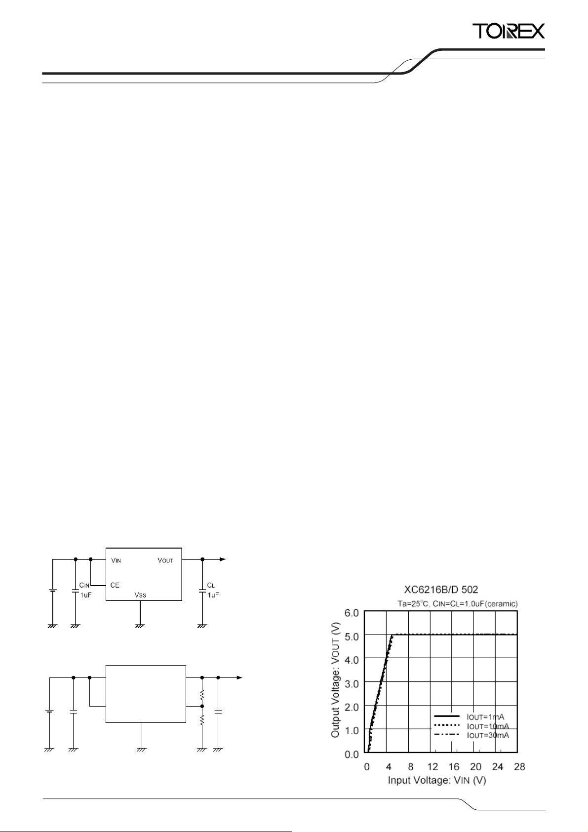
■ TYPICAL APPLICATION CIRCUIT
Fixed Output Voltage
ment
■FEATURES
Max Output Current : More than 150mA (200mA limit)
Dropout Voltage
Input Voltage Range
Output Voltage Range
(V
: 300mV@I
: 2.0V~28.0V
: 2.0V~12.0V (0.1V increments)
IN=VOUT
+3.0V)
OUT=20mA
2.0V~23V with external resistors
Fixed Output Accuracy :±2%
±1% optional for XC6216 series
Low Power Consumption : 5μA
Stand-by Current : Less than 0.1μA
High Ripple Rejection : 30dB@1kHz
Operating Temperature : -40℃~+85℃
Low ESR Capacitor : Ceramic Capacitor Compatible
Built–in Protection : Current Limit Circuit
Thermal Shutdown Circuit
Operating Ambient Temperature -40℃~+85℃
Packages : SOT-25, SOT-89, SOT-89-5,
SOP-8FD(Under Development)
USP-6C, SOT-223, TO-252
Environmentally Friendly : EU RoHS Compliant, Pb Free
■ TYPICAL PERFORMANCE
CHARACTERISTICS
●Output Voltage vs. Input Volatage
L) is
VIN VOUT
R
R
100kΩ
21
1uF
22
CIN CL
1uF
CE VOFB
VSS
設定電圧外部設定品
Output Voltage External Setting
XC6216C/XE6216Cシリーズ
XC6126C Series
1/45

XC6216/XE6216 Series
■PIN CONFIGURATION
SOT-25
(TOP VIEW)
SOT-223
(TOP VIEW)
■PIN ASSIGNMENT
●XC6216 Series B Type
PIN NUMBER
SOT-25 SOT-89-5 USP-6C
1 5 6
2 2 5
3 4 2,4
4 3 3
5 1 1
●XC6216 Series C Type
PIN NUMBER
SOT-25 SOT-89-5 USP-6C
1 5 6
2 2 5
3 4 4
4 3 3
5 1 1
- - 2
●XC6216 Series D Type
PIN NUMBER
SOT-89 SOT-223 TO-252
3 3 1 VIN Power Input
2 2 2 VSS Ground
1 1 3 V
2/45
SOT-89
(TOP VIEW)
(TOP VIEW)
SOT-89-5
(TOP VIEW)
TO-252
(TOP VIEW)
(Under Development)
SOP-8FD
(Under Development)
8
6
2,3,5,7
4
1
SOP-8FD
(Under Development)
8
6
5
4
1
2,3,7
PIN NAME FUNCTIONS
VIN Power Input
VSS Ground
NC No connection
CE ON/OFF Control
V
OUT
PIN NAME FUNCTIONS
VIN Power Input
VSS Ground
V
OFB
CE ON/OFF Control
V
OUT
NC No connection
PIN NAME FUNCTIONS
Output
OUT
USP-6C
(BOTTOM VIEW)
* The dissipation pad for the USP-6C
package should be solder-plated in
reference mount pattern and metal
masking so as to enhance mounting
strength and heat release. If the pad
needs to be connected to other pins, it
should be connected to the VSS (No. 5)
pin.
SOP-8FD
Output
Output Voltage
Adjustment
Output

■PIN ASSIGNMENT
●XE6216 Series B Type
PIN
NUMBER
SOT-89-5
1 V
2 VSS Ground
3 CE ON/OFF Control
4 NC No connection
5 VIN Power Input
■LOGIC CONDITION FOR THE PIN
PIN NAME DESIGNATOR CONDITIONS IC OPERATION
CE
* Please avoid the state of OPEN, and make CE Pin arbitrary fixed potential.
(XC6216 Series B Type, XE6216 Series B Type, XC6216 Series C Type)
■PIN FUNCTION ASSIGNMENT
XC6216 Series B Type/XE6216 Series B Type Available
PIN NAME FUNCTIONS
Output
OUT
L
H
0V≦V
1.1V≦V
≦0.35V
CE
≦28.0V
CE
OPEN CE=OPEN Undefined state
SERIES CHIP ENABLE PIN
XC6216 Series C Type Available
XC6216 Series D Type Not Available
XC6216/XE6216
Series
OFF
ON
3/45
(*1)
(*1)
(*1)
XC6216/XE6216 Series
■ PRODUCT CLASSIFICATION
●Ordering Information
XC6216①②③④⑤⑥-⑦
DESIGNATOR ITEM SYMBOL DESCRIPTION
①
Type and Options of
②③ Output Voltage
: CE function (Active High) Fixed output voltage 2.0V~12.0V(0.1V increments)
B Fixed output voltage, 2.0V~12.0V(0.1V increments)
Regulators
C Output voltage externally set (V
For the voltage within 2.0V ~9.9V (0.1V increments);
e.g. 2.5V ⇒ 25, 5.0V ⇒ 50
20 ~ C0
For the voltage within 10.0V~12.0V (0.1V increments);
e.g. 10.6V ⇒ A6, 11.2V ⇒ B2, 12.0V ⇒ C0
OFB
=2.0V)
20 For C type (output voltage externally set), V
④
Output Voltage
Accuracy
(*2)
2 ±2%
1 ±1%
MR SOT-25 (3,000/Reel)
MR-G SOT-25 (3,000/Reel)
PR SOT-89-5 (1,000/Reel)
PR-G SOT-89-5 (1,000/Reel)
⑤⑥-⑦
(*1)
Packages (Order Unit)
ER USP-6C (3,000/Reel)
ER-G USP-6C (3,000/Reel)
QR-G SOP-8FD (1,000/Reel) (Under Development)
(*1)
The “-G” suffix denotes Halogen and Antimony free as well as being fully RoHS compliant.
(*2)
For the Type C, the accuracy is based on V
voltage. The actual output voltage accuracy is depended on the external resistances.
OFB
XC6216D①②③④⑤-⑥
DESIGNATOR ITEM SYMBOL DESCRIPTION
①② Output Voltage 20 ~ C0
③
④⑤-⑥
(*1)
The “-G” suffix denotes Halogen and Antimony free as well as being fully RoHS compliant.
XE6216B①②③④⑤-⑥
DESIGNATOR ITEM SYMBOL DESCRIPTION
④⑤-⑥
(*1)
The “-G” suffix denotes Halogen and Antimony free as well as being fully RoHS compliant.
(*1)
Packages (Order Unit)
①②
③
(*1)
Package (Order Unit)
: 3 pin regulator (No CE function), Fixed output voltage 2.0V~12.0V(0.1V increments)
For the voltage within 2.0V~9.9V (0.1V increments);
e.g. 2.5V ⇒ 25, 5.0V ⇒ 50
For the voltage within10.0V~12.0V (0.1V increments);
e.g. 10.6V ⇒ A6, 11.2V ⇒ B2, 12.0V ⇒ C0
Output Voltage
Accuracy
2 ±2%
1 ±1%
PR SOT-89 (1,000/Reel)
PR-G SOT-89 (1,000/Reel)
FR SOT-223 (1,000/Reel)
FR-G SOT-223 (1,000/Reel)
JR TO-252 (2,500/Reel)
JR-G TO-252 (2,500/Reel)
: CE function (Active High), Fixed output voltage 2.0V~12.0V(0.1V increments)
Characteristics are guaranteed over the temperature range of -40℃ to 85℃.
For the voltage within 2.0V ~9.9V (0.1V increments);
Output Voltage 20~C0
e.g. 2.5V ⇒ 25, 5.0V ⇒ 50
For the voltage within 10.0V~12.0V (0.1V increments);
e.g. 10.6V ⇒ A6, 11.2V ⇒ B2, 12.0V ⇒ C0
Output Voltage
Accuracy
2
PR
PR-G
±2%
SOT-89-5 (1,000/Reel)
SOT-89-5 (1,000/Reel)
OFB=2.0V only
4/45

■ BLOCK DIAGRAMS
●XC6216 Series
●XC6216 Series B Type
●XC6216 Series C Type
●XC6216 Series D Type
●XE6216 Series
●XE6216 Series B Type
*Diodes inside the circuit are an ESD protection diode and parasitic diodes.
XC6216/XE6216
Series
5/45
XC6216/XE6216 Series
■ABSOLUTE MAXIMUM RATINGS
●XC6216 Series B Type
PAR AMETER SYMBOL RATINGS UNITS
Input Voltage VIN VSS-0.3~+30 V
Output Current IOUT 300
Output Voltage VOUT VSS-0.3~VIN+0.3 V
CE Input Voltage VCE VSS-0.3~30 V
Power Dissipation
SOT-25
SOT-89-5
Pd
USP-6C
600 (PCB mounted)
1300 (PCB mounted)
1000 (PCB mounted)
SOP-8FD
(Under Development)
1500(PCB mounted)
Operating Ambient Temperature Topr -40~+85
Storage Temperature Tstg -55~+125
*1: Pd > (V
*2: The power dissipation figure shown is PCB mounted. Please refer to pages 38 ~ 42 for details.
●XC6216 Series C Type
IN-VOUT
)×I
OUT
PAR AMETER SYMBOL RATINGS UNITS
Input Voltage VIN VSS-0.3~+30 V
Output Current IOUT 300
Output Voltage VOUT VSS-0.3~VIN+0.3 V
CE Input Voltage VCE VSS-0.3 ~ +30 V
FB Voltage VOFB VSS-0.3 ~ +30 V
Power Dissipation
SOT-25
SOT-89-5
Pd
USP-6C
600 (PCB mounted)
1300 (PCB mounted)
1000 (PCB mounted)
SOP-8FD
(Under Development)
1500(PCB mounted)
Operating Ambient Temperature Topr -40~+85
Storage Temperature Tstg -55~+125
)×I
*1: Pd > (V
*2: The power dissipation figure shown is PCB mounted. Please refer to pages 38 ~ 42 for details.
●XC6216D Series
IN-VOUT
OUT
PAR AMETER SYMBOL RATINGS UNITS
Input Voltage VIN VSS-0.3~+30 V
Output Current IOUT 300
Output Voltage VOUT VSS-0.3~VIN+0.3 V
SOT-89 500
Power Dissipation
SOT-223
Pd
1500 (PCB mounted)
TO-252
Operating Ambient Temperature Topr -40~+85
Storage Temperature Tstg -55~+125
*1: Pd > (VIN-V
*2: The power dissipation figure shown is PCB mounted. Please refer to pages 38 ~ 42 for details.
OUT
)×I
OUT
(*1)
mA
250
500
120
300
(*1)
mA
250
500
120
300
(*1)
mA
300
500
(*2)
(*2)
(*2)
(*2)
(*2)
(*2)
(*2)
(*2)
(*2)
mW
(Ta=25℃)
℃
℃
mW
(Ta=25℃)
℃
℃
mW
(Ta=25℃)
℃
℃
6/45
■ABSOLUTE MAXIMUM RATINGS (Continued)
●XE6216 Series B Type
PAR AMETER SYMBOL RATINGS UNITS
Input Voltage VIN
Output Current I
Output Voltage V
300
OUT
OUT
CE Input Voltage VCE
Power Dissipation SOT-89-5 Pd
1300 (PCB mounted)
Operating Ambient Temperature Topr
Junction Temperature TJ
Storage Temperature Tstg
*1: Pd > (VIN-V
*2: The power dissipation figure shown is PCB mounted. Please refer to pages 38 ~ 42 for details.
OUT
)×I
OUT
-0.3~+30
V
SS
(*1)
mA
-0.3~VIN+0.3
V
SS
-0.3~+30
V
SS
500
-40~+85 ℃
-40~+125 ℃
-55~+125 ℃
(*2)
XC6216/XE6216
Series
V
V
V
mW
(Ta =2 5℃)
7/45

XC6216/XE6216 Series
■ELECTRICAL CHARACTERISTICS
●XC6216 Series B Type
PAR AMETER SYMBOL CONDITIONS MIN. TYP. MAX. UNITS CIRCUIT
Output Voltage V
Maximum Output Current I
Load Regulation
Dropout Voltage 1 Vdif1
(*2)
OUT(E)
OUTMAX
△V
I
OUT
(*3)
I
OUT
VIN=V
OUT(T)
V
IN=VOUT(T)
1mA≦I
(2.0V≦V
1mA≦I
( 7.0<V
OUT
=20mA, VCE=VIN E-0 V
+3.0V, VCE=V
(V
OUT(T)
+3.0V, VCE=V
(V
OUT(T)
≦50mA, VCE=VIN
OUT
OUT(T)
≦50mA , VCE=V
OUT
OUT(T)
=20mA, VCE=VIN
≧3.0V)
<3.0V)
≦7.0V)
≦12.0V )
Ta =2 5℃
①
(*1)
IN
IN
150 - -
(*1)
100 - -
- 50 90
IN
- 110 140
- E-1
mA
mA
mV
mV
mV
①
①
①
①
①
Dropout Voltage 2 Vdif2
Supply Current ISS V
Stand-by Current I
Line Regulation 1
Line Regulation 2
(△V
(△V
Input Voltage VIN
Output Voltage
Temperature Characteristics
(△Topr・V
Ripple Rejection Rate PSRR
Short Current I
CE ”H” Level Voltage V
CE ”L” Level Voltage V
CE ”H” Level Current I
CE ”L” Level Current I
Thermal Shutdown
Detect Temperature
Thermal Shutdown
Release Temperature
Hysteresis Width T
Unless otherwise stated, V
NOTE:
*1: V
*2: V
(i.e. the output voltage when “V
*3: Vdif={V
: Nominal output voltage
OUT(T)
: Effective output voltage
OUT(E)
- V
IN1
OUT1
V
: V
OUT1
V
: The input voltage when V
IN1
<3.0V, A voltage equal to 98% of the output voltage whenever an amply stabilized I
OUT(T)
V
≧3.0V, A voltage equal to 98% of the output voltage whenever an amply stabilized I
OUT(T)
IN=VOUT(T)
}
(*3)
I
V
STB
/
△V
OUT
OUT
OUT
/
/
OUT
)
)
)
IN・VOUT
△V
IN・VOUT
△V
VIN=[V
V
SHORT
-
CEH
-
CEL
V
CEH
V
CEL
T
TSD
T
TSR
TSD-TTSR
+2.0V.
OUT1
+2.0V” is provided at the V
OUT(T)
appears as input voltage is gradually decreased.
=100mA , VCE=VIN
OUT
CE=VIN
CE=VSS
+2.0V≦VIN≦28.0V
V
OUT(T)
I
=5mA, VCE=VIN
OUT
+2.0V≦VIN≦28.0V
V
OUT(T)
I
=13mA, VCE=VIN
OUT
I
=20mA, VCE=VIN
OUT
-40℃≦Topr≦85℃
+2.0]V+0.5Vp-pAC
OUT(T)
I
=20mA, f=1kHz, VCE=V
OUT
IN=VCE
=28.0V, VCE=VSS
IN
CE=VIN
=28.0V
V
CE=VIN
(*1)
Junction Temperature
VCE=VIN
Junction Temperature
VCE=VIN
Junction Temperature
IN
- E-2
1 5 9
- 0.01 0.10
(*1)
- 0.05 0.10
(*1)
- 0.15 0.30
2.0 - 28.0
- ±100 -
(*1)
- 30 -
IN
- 30 -
1.1 - 28.0
0 - 0.35
-0.1 - 0.1
-0.1 - 0.1
- 150 -
- 125 -
- 25 -
pin while maintaining a certain I
OUT{VOUT(T)
OUT{VOUT(T)
mV
μA ②
μA ②
%/V ①
%/V ①
V -
ppm/℃ ①
dB
mA
V
V
μA ①
μA ①
℃ ①
℃ ①
℃
value.)
OUT
+3.0V} is input.
+2.0V} is input.
①
③
①
①
①
-
8/45

■ELECTRICAL CHARACTERISTICS (Continued)
●XC6216 Series C Type
PAR AMETER SYMBOL CONDITIONS MIN. TYP. MAX. UNITS CIRCUIT
XC6216/XE6216
Series
Ta =2 5℃
Output Voltage (Accuracy±2%)
Output Voltage (Accuracy±1%)
V
V
OUT(E)
OUT(E)
Divided Resistor RFB
Maximum Output Current I
Load Regulation
OUTMAX
△V
Dropout Voltage1 Vdif1
Dropout Voltage2 Vdif2
Supply Current ISS V
Stand-by Current I
Line Regulation1
Line Regulation2
△V
(△V
△V
(△VIN・V
Input Voltage VIN
Output Voltage
Temperature Characteristics
△V
(△Topr・V
Ripple Rejection Rate PSRR
Short Current I
CE ”H” Level Voltage V
CE ”L” Level Voltage V
CE ”H” Level Current I
CE ”L” Level Current I
Thermal Shutdown Detect
Temperature
Thermal Shutdown Release
Temperature
Hysteresis Width T
NOTE:
*1: V
*2: V
(i.e. the output voltage when “V
*3: Vdif={V
: Nominal output voltage C type is 2.0v
OUT(T)
: Effective output voltage
OUT(E)
- V
IN1
V
: V
OUT1
V
V
: The input voltage when V
IN1
}
OUT1
<3.0V, A voltage equal to 98% of the output voltage whenever an amply stabilized I
OUT(T)
≧3.0V, A voltage equal to 98% of the output voltage whenever an amply stabilized I
OUT(T)
TSD-TTSR
OUT
(*2)
(*2)
VIN=4.0V, I
V
CE=VIN
VIN=4.0V, I
V
CE=VIN
V
IN=VOUT
V
VIN=5.0V, VCE=VIN ,
V
=20mA ,
OUT
, V
OFB=VOUT
=20mA ,
OUT
, V
OFB=VOUT
=5.0V, VCE=VSS
OFB=VOUT
OFB=VOUT
VIN=4.0V
OUT
(*3)
I
(*3)
I
VIN=4.0V, VCE=V
STB
/
OUT
IN・VOUT
SHORT
T
T
)
/
OUT
)
OUT
/
OUT
)
OUT
V
CEH
V
CEL
CEH
CEL
TSD
TSR
OUT(T)
1 appears as input voltage is gradually decreased.
1mA≦I
V
CE=VIN
=20mA, VCE=VIN, V
OUT
=100mA, VCE=VIN, V
OUT
=4.0V, VCE=VIN, V
IN
4.0V≦V
=5mA, VCE=VIN,V
I
OUT
≦50mA,
OUT
, V
OFB=VOUT
SS
≦28.0V,
IN
OFB=VOUT
OFB=VOUT
OFB=VOUT
, V
OFB=VOUT
OFB=VOUT
4.0V≦VIN≦28.0V,
I
=13mA, VCE=VIN, V
OUT
VIN=4.0V, I
V
OFB=VOUT
V
IN
I
=20mA, f=1kHz, VCE=VIN
OUT
=20mA , VCE=V
OUT
, -40℃≦Topr≦85℃
=4.0V+0.5Vp-pAC,
V
OFB=VOUT
V
=4.0V, VCE=VIN,
IN
V
OFB=VOUT
=4.0V, V
IN
=4.0V, V
IN
V
IN=VCE
V
OFB=VOUT
OFB=VOUT
OFB=VOUT
OFB=VOUT
=28.0V,
IN,
VIN=28.0V, VCE=VSS
V
OFB=VOUT
VIN=4.0V , VCE=VIN
Junction Temperature
VIN=4.0V , VCE=VIN
Junction Temperature
VIN=4.0V , VCE=VIN
Junction Temperature
+2.0V” is provided at the VIN pin while maintaining a certain I
1.96 2.00 2.04
1.98 2.00 2.02
1.70 4.10 6.30
100 - -
- 50 90
- 450 600
- 1900 2600
1 5 9
- 0.01 0.10
- 0.05 0.10
- 0.15 0.30
2.0 - 28.0
- ±100 -
ppm/℃ ①
- 30 -
- 30 -
1.1 - 28.0
0 - 0.35
-0.1 - 0.1
-0.1 - 0.1
- 150 -
- 125 -
- 25 -
value.)
OUT
OUT{VOUT(T)
OUT{VOUT(T)
+3.0V} is input.
+2.0V} is input.
V
①
MΩ ④
mA
mV
mV
mV
①
①
①
①
μA ②
μA ②
%/V ①
%/V ①
V -
dB
mA
V
V
③
①
①
①
μA ①
μA ①
℃ ①
℃ ①
℃
-
9/45

XC6216/XE6216 Series
■ELECTRICAL CHARACTERISTICS (Continued)
●XC6216 Series D type
PAR AMETER SYMBOL CONDITIONS MIN. TYP. MAX. UNITS CIRCUIT
Ta =2 5℃
Output Voltage V
Maximum Output Current I
Load Regulation
Dropout Voltage1 Vdif1
Dropout Voltage2 Vdif2
(*2)
OUT(E)
I
VIN=V
(V
OUTMAX
V
IN=VOUT(T)
(V
1mA≦I
△V
OUT
( 2.0V≦V
1mA≦I
( 7.0V<V
(*3)
I
(*3)
I
=20mA E-0 V
OUT
+3.0V
OUT(T)
≧3.0V)
OUT(T)
+3.0V
<3.0V)
OUT(T)
≦50mA
OUT
≦7.0V )
OUT(T)
≦50mA
OUT
≦12.0V )
OUT(T)
=20mA
OUT
=100mA
OUT
Supply Current ISS
Line Regulation1
Line Regulation2
(△V
(△V
OUT
IN・VOUT
△V
OUT
IN・VOUT
/
)
/
)
+2.0V≦VIN≦28.0V
V
OUT(T)
I
OUT
+2.0V≦VIN≦28.0V
V
OUT(T)
I
OUT
=5mA
=13mA
△V
Input Voltage VIN
Output Voltage
Temperature Characteristics
△V
(△Topr・V
Ripple Rejection Rate PSRR
Short Current I
Thermal Shutdown Detect
Temperature
Thermal Shutdown Release
Temperature
Hysteresis Width T
Unless otherwise stated, VIN=V
NOTE:
*1: V
*2: V
(i.e. the output voltage when “V
*3: Vdif={V
: Nominal output voltage
OUT(T)
: Effective output voltage
OUT(E)
- V
IN1
V
: V
OUT1
OUT(T)
V
OUT(T)
V
: The input voltage when V
IN1
}
OUT1
<3.0V, A voltage equal to 98% of the output voltage whenever an amply stabilized I
≧3.0V, A voltage equal to 98% of the output voltage whenever an amply stabilized I
TSD-TTSR
OUT(T)
/
OUT
)
OUT
VIN=[V
V
SHORT
T
Junction Temperature - 150 -
TSD
T
Junction Temperature - 125 -
TSR
Junction Temperature - 25 -
+2.0V.
+2.0V” is provided at the V
OUT(T)
appears as input voltage is gradually decreased.
OUT1
I
=20mA
OUT
-40℃≦Topr≦85℃
+2.0]V+0.5Vp-pAC
OUT(T)
I
=20mA, f=1kHz
OUT
IN=VOUT(T)
+2.0V
IN
(*1)
(*1)
150 - -
100 - -
- 50 90
- 110 140
- E-1
- E-2
1 5 9
(*1)
- 0.05 0.10
(*1)
- 0.15 0.30
2.0 - 28.0
- ±100 -
(*1)
- 30 -
(*1)
pin while maintaining a certain I
- 30 -
OUT{VOUT(T)
OUT{VOUT(T)
mA
mA
mV
mV
mV
mV
μA ②
%/V ①
%/V ①
V -
ppm/℃ ①
dB
mA
℃ ①
℃ ①
℃
value.)
OUT
+3.0V} is input.
+2.0V} is input.
①
①
①
①
①
①
①
③
①
-
10/45

XC6216/XE6216
■ELECTRICAL CHARACTERISTICS (Continued)
●Voltage Chart (XC6216 Series)
PAR AMETER E-0 E-1 E-2
NOMINAL
OUTPUT
VOLTAGE(V)
V
OUT(T)
2.0 1.960 2.040 1.980 2.020 450 600 1900 2600
2.1 2.058 2.142 2.079 2.121 450 600 1900 2600
2.2 2.156 2.244 2.178 2.222 390 520 1700 2200
2.3 2.254 2.346 2.277 2.323 390 520 1700 2200
2.4 2.352 2.448 2.376 2.424 390 520 1700 2200
2.5 2.450 2.550 2.475 2.525 310 450 1500 1900
2.6 2.548 2.652 2.574 2.626 310 450 1500 1900
2.7 2.646 2.754 2.673 2.727 310 450 1500 1900
2.8 2.744 2.856 2.772 2.828 310 450 1500 1900
2.9 2.842 2.958 2.871 2.929 310 450 1500 1900
3.0 2.940 3.060 2.970 3.030 260 360 1300 1700
3.1 3.038 3.162 3.069 3.131 260 360 1300 1700
3.2 3.136 3.264 3.168 3.232 260 360 1300 1700
3.3 3.234 3.366 3.267 3.333 260 360 1300 1700
3.4 3.332 3.468 3.366 3.434 260 360 1300 1700
3.5 3.430 3.570 3.465 3.535 260 360 1300 1700
3.6 3.528 3.672 3.564 3.636 260 360 1300 1700
3.7 3.626 3.774 3.663 3.737 260 360 1300 1700
3.8 3.724 3.876 3.762 3.838 260 360 1300 1700
3.9 3.822 3.978 3.861 3.939 260 360 1300 1700
4.0 3.920 4.080 3.960 4.040 220 320 1100 1500
4.1 4.018 4.182 4.059 4.141 220 320 1100 1500
4.2 4.116 4.284 4.158 4.242 220 320 1100 1500
4.3 4.214 4.386 4.257 4.343 220 320 1100 1500
4.4 4.312 4.488 4.356 4.444 220 320 1100 1500
4.5 4.410 4.590 4.455 4.545 220 320 1100 1500
4.6 4.508 4.692 4.554 4.646 220 320 1100 1500
4.7 4.606 4.794 4.653 4.747 220 320 1100 1500
4.8 4.704 4.896 4.752 4.848 220 320 1100 1500
4.9 4.802 4.998 4.851 4.949 220 320 1100 1500
OUTPUT VOLTAGE
(V)
2% ACCURACY
V
V
OUT(E)
OUTPUT VOLTAGE
(V)
1% ACCURACY
Vdif1 Vdif2
OUT(E)
DROPOUT VOLTAGE 1
(mV)
I
=20mA
OUT
DROPOUT VOLTAGE 2
I
OUT
MIN. MAX. MIN. MAX. TYP. MAX. TYP. MAX.
Series
(mV)
=100mA
11/45

XC6216/XE6216 Series
■ELECTRICAL CHARACTERISTICS (Continued)
●Voltage Chart (XC6216 Series) (Continued)
PAR AMETER E-0 E-1 E-2
NOMINAL
OUTPUT
VOLTAGE(V)
V
OUT(T)
5.0 4.900 5.100 4.950 5.050 190 280 1000 1300
5.1 4.998 5.202 5.049 5.151 190 280 1000 1300
5.2 5.096 5.304 5.148 5.252 190 280 1000 1300
5.3 5.194 5.406 5.247 5.353 190 280 1000 1300
5.4 5.292 5.508 5.346 5.454 190 280 1000 1300
5.5 5.390 5.610 5.445 5.555 190 280 1000 1300
5.6 5.488 5.712 5.544 5.656 190 280 1000 1300
5.7 5.586 5.814 5.643 5.757 190 280 1000 1300
5.8 5.684 5.916 5.742 5.916 190 280 1000 1300
5.9 5.782 6.018 5.841 5.959 190 280 1000 1300
6.0 5.880 6.120 5.940 6.060 190 280 1000 1300
6.1 5.978 6.222 6.039 6.161 190 280 1000 1300
6.2 6.076 6.324 6.138 6.262 190 280 1000 1300
6.3 6.174 6.426 6.237 6.363 190 280 1000 1300
6.4 6.272 6.528 6.336 6.464 190 280 1000 1300
6.5 6.370 6.630 6.435 6.565 170 230 800 1150
6.6 6.468 6.732 6.534 6.666 170 230 800 1150
6.7 6.566 6.834 6.633 6.767 170 230 800 1150
6.8 6.664 6.936 6.732 6.868 170 230 800 1150
6.9 6.762 7.038 6.831 6.969 170 230 800 1150
7.0 6.860 7.140 6.930 7.070 170 230 800 1150
7.1 6.958 7.242 7.029 7.171 170 230 800 1150
7.2 7.056 7.344 7.128 7.272 170 230 800 1150
7.3 7.154 7.446 7.227 7.373 170 230 800 1150
7.4 7.252 7.548 7.326 7.474 170 230 800 1150
7.5 7.350 7.650 7.425 7.575 170 230 800 1150
7.6 7.448 7.752 7.524 7.676 170 230 800 1150
7.7 7.546 7.854 7.623 7.777 170 230 800 1150
7.8 7.644 7.956 7.722 7.878 170 230 800 1150
7.9 7.742 8.058 7.821 7.979 170 230 800 1150
8.0 7.840 8.160 7.920 8.080 170 230 800 1150
OUTPUT VOLTAGE
(V)
2% ACCURACY
V
V
OUT(E)
OUTPUT VOLTAGE
(V)
1% ACCURACY
Vdif1 Vdif2
OUT(E)
DROPOUT VOLTAGE 1
(mV)
I
=20mA
OUT
DROPOUT VOLTAGE 2
I
OUT
MIN. MAX. MIN. MAX. TYP. MAX. TYP. MAX.
(mV)
=100mA
12/45

XC6216/XE6216
■ELECTRICAL CHARACTERISTICS (Continued)
●Voltage Chart (XC6216 Series) (Continued)
PAR AMETER E-0 E-1 E-2
NOMINAL
OUTPUT
VOLTAGE(V)
V
OUT(T)
8.1 7.938 8.262 8.019 8.181 130 190 700 950
8.2 8.036 8.364 8.118 8.282 130 190 700 950
8.3 8.134 8.466 8.217 8.383 130 190 700 950
8.4 8.232 8.568 8.316 8.484 130 190 700 950
8.5 8.330 8.670 8.415 8.585 130 190 700 950
8.6 8.428 8.772 8.514 8.686 130 190 700 950
8.7 8.526 8.874 8.613 8.787 130 190 700 950
8.8 8.624 8.976 8.712 8.888 130 190 700 950
8.9 8.722 9.078 8.811 8.989 130 190 700 950
9.0 8.820 9.180 8.910 9.090 130 190 700 950
9.1 8.918 9.282 9.009 9.191 130 190 700 950
9.2 9.016 9.384 9.108 9.292 130 190 700 950
9.3 9.114 9.486 9.207 9.393 130 190 700 950
9.4 9.212 9.588 9.306 9.494 130 190 700 950
9.5 9.310 9.690 9.405 9.595 130 190 700 950
9.6 9.408 9.792 9.504 9.696 130 190 700 950
9.7 9.506 9.894 9.603 9.797 130 190 700 950
9.8 9.604 9.996 9.702 9.898 130 190 700 950
9.9 9.702 10.098 9.801 9.999 130 190 700 950
10.0 9.800 10.200 9.900 10.100 130 190 700 950
10.1 9.898 10.302 9.999 10.201 120 160 650 850
10.2 9.996 10.404 10.098 10.302 120 160 650 850
10.3 10.094 10.506 10.197 10.403 120 160 650 850
10.4 10.192 10.608 10.296 10.504 120 160 650 850
10.5 10.290 10.710 10.395 10.605 120 160 650 850
10.6 10.388 10.812 10.494 10.706 120 160 650 850
10.7 10.486 10.914 10.593 10.807 120 160 650 850
10.8 10.584 11.016 10.692 10.908 120 160 650 850
10.9 10.682 11.118 10.791 11.009 120 160 650 850
11.0 10.780 11.220 10.890 11.110 120 160 650 850
11.1 10.878 11.322 10.989 11.211 120 160 650 850
11.2 10.976 11.424 11.088 11.312 120 160 650 850
11.3 11.074 11.526 11.187 11.413 120 160 650 850
11.4 11.172 11.628 11.286 11.514 120 160 650 850
11.5 11.270 11.730 11.385 11.615 120 160 650 850
11.6 11.368 11.832 11.484 11.716 120 160 650 850
11.7 11.466 11.934 11.583 11.817 120 160 650 850
11.8 11.564 12.036 11.682 11.918 120 160 650 850
11.9 11.662 12.138 11.781 12.019 120 160 650 850
12.0 11.760 12.240 11.880 12.120 120 160 650 850
OUTPUT VOLTAGE
(V)
2% ACCURACY
V
V
OUT(E)
OUTPUT VOLTAGE
(V)
1% ACCURACY
Vdif1 Vdif2
OUT(E)
DROPOUT VOLTAGE 1
(mV)
I
=20mA
OUT
DROPOUT VOLTAGE 2
(mV)
I
=100mA
OUT
MIN. MAX. MIN. MAX. TYP. MAX. TYP. MAX.
Series
13/45

A
XC6216/XE6216 Series
■ELECTRICAL CHARACTERISTICS (Continued)
●XE6216 Series B Type
PAR AMETER SYMBOL CONDITIONS
Output Voltage V
Maximum Output
Current
Load Regulation
(*)
(*)
ΔV
OUT(E)
I
OUTMAX
OUT
(*2)
I
OUT
VIN=V
= V
V
IN
V
CE=VIN
=20mA , VCE=VIN
+3.0V, VCE=V
OUT(T)
(V
≧3.0V)
OUT(T)
+3.0V, VCE=V
OUT(T)
(V
<3.0V)
OUT(T)
, 1mA≦I
OUT
IN
IN
≦50m
(*1)
(*1)
Ta=25℃ Ta=-40℃~85℃
MIN. TYP. MAX. MIN. TYP. MAX.
E-0-1 E-0-2 V
- - - 150 - - mA
- - - 100 - - mA
- E-1-1 - E-1-2 mV
UNITS
CIRCUIT
①
①
①
①
Dropout Voltage1 Vdif1
Dropout Voltage2
(*)
Vdif2
Supply Current ISS V
Stand-by Current I
Line Regulation1
Line Regulation2
(*)
(*)
(ΔV
(ΔVIN・V
(*3)
(*3)
V
STB
ΔV
/
OUT
OUT
/
OUT
)
)
IN・VOUT
ΔV
=20mA, VCE=VIN
I
OUT
=100mA, VCE=VIN
I
OUT
V
+2.0V≦VIN≦28.0V
OUT(T)
I
=5mA, VCE=VIN
OUT
+2.0V≦VIN≦28.0V
V
OUT(T)
I
=13mA, VCE=VIN
OUT
CE=VIN
CE=VSS
1 5 9 0.5 5 10
- 0.01 0.1 - 0.01 4
- E-2-1 - E-2-2 mV
- E-3-1 - E-3-2 mV
μA ②
μA ②
(*1)
- 0.05 0.10 - 0.05 0.12 %/V
(*1)
- 0.15 0.30 - 0.15 0.32 %/V
Input Voltage VIN 2.0 28.0 2.0 28.0 V
Output Voltage
Temperature
Characteristics
Ripple Rejection Rate PSRR
Short Current I
CE "H" Level Voltage V
CE "L" Level Voltage V
CE "H" Level Current I
CE "L" Level Current I
Thermal Shutdown
Detect Temperature
ΔV
OUT
(ΔTopr・V
SHORT
CEH
CEL
CEH
CEL
T
TSD
/
OUT
V
I
=20mA, VCE=VIN
OUT
)
-40℃≦Topr≦85℃
VIN=[V
+2.0]V+0.5Vp-pAC
OUT(T)
I
=20mA, f=1kHz ,
OUT
V
- ±100 ±350 - - -
(*1)
ppm/
- 30 - - 30 - dB
CE=VIN
- 30 - - 30 - mA
CE=VIN
- - - - 1.1 - 28.0 V
- - - - 0 - 0.35 V
V
V
IN
Junction Temperature
=28.0V -0.1 - 0.1 -0.1 - 0.7
IN=VCE
=28.0V, VCE=VSS -0.1 - 0.1 -0.2 - -0.2
V
CE=VIN、
- 150 - - 150 -
μA ②
μA ②
℃ ①
℃
①
①
①
①
①
③
①
①
①
Thermal Shutdown
Release Temperature
Hysteresis Width T
Unless otherwise stated, V
NOTE:
*1: V
OUT(T): Nominal output voltage
*2: V
OUT(E): Effective output voltage
(i.e. the output voltage when “V
*3: Vdif={V
V
IN1- VOUT1}
V
OUT1: V
V
IN1: The input voltage when VOUT1 appears as input voltage is gradually decreased.
(*)Junction temperature range is Tj=-40~125℃ for this table.
<3.0V, A voltage equal to 98% of the output voltage whenever an amply stabilized IOUT{VOUT(T)+3.0V} is input.
OUT(T)
≧3.0V, A voltage equal to 98% of the output voltage whenever an amply stabilized IOUT{VOUT(T)+2.0V} is input.
OUT(T)
14/45
T
TSR
TSD - TTSR
IN=VOUT(T)+2.0V.
OUT(T)+2.0V” is provided at the VIN pin while maintaining a certain IOUT value.)
V
CE=VIN、
Junction Temperature
VCE=V
IN、
Junction Temperature
- 125 - - 125 -
- 25 - - 25 -
℃ ①
℃
-

■ELECTRICAL CHARACTERISTICS (Continued)
●Voltage Chart 1 (XE6216 Series)
SYMBOL
Temperature
/ Ta
PARAMETER
NOMINAL
OUTPUT
VOLTAGE(V)
V
OUT(T)
OUTPUT VOLTAGE (V)
E-0-1 E-0-2
25℃ -40~85℃
OUTPUT VOLTAGE (V)
Accuracy ±2%
V
V
OUT(E)
Accuracy +3% , -3.5%
OUT(E)
MIN. MAX. MIN. MAX.
2.0 1.960 2.040 1.930 2.060
2.1 2.058 2.142 2.027 2.163
2.2 2.156 2.244 2.123 2.266
2.3 2.254 2.346 2.220 2.369
2.4 2.352 2.448 2.316 2.472
2.5 2.450 2.550 2.413 2.575
2.6 2.548 2.652 2.509 2.678
2.7 2.646 2.754 2.606 2.781
2.8 2.744 2.856 2.702 2.884
2.9 2.842 2.958 2.799 2.987
3.0 2.940 3.060 2.895 3.090
3.1 3.038 3.162 2.992 3.193
3.2 3.136 3.264 3.088 3.296
3.3 3.234 3.366 3.185 3.399
3.4 3.332 3.468 3.281 3.502
3.5 3.430 3.570 3.378 3.605
3.6 3.528 3.672 3.474 3.708
3.7 3.626 3.774 3.571 3.811
3.8 3.724 3.876 3.667 3.914
3.9 3.822 3.978 3.764 4.017
4.0 3.920 4.080 3.860 4.120
4.1 4.018 4.182 3.957 4.223
4.2 4.116 4.284 4.053 4.326
4.3 4.214 4.386 4.150 4.429
4.4 4.312 4.488 4.246 4.532
4.5 4.410 4.590 4.342 4.635
4.6 4.508 4.692 4.439 4.738
4.7 4.606 4.794 4.535 4.841
4.8 4.704 4.896 4.632 4.944
4.9 4.802 4.998 4.728 5.047
SYMBOL
Temperature
/ Ta
PAR AM ETE R
NOMINAL
OUTPUT
VOLTAGE(V)
V
OUT(T)
5.0 4.900 5.100 4.825 5.150
5.1 4.998 5.202 4.921 5.253
5.2 5.096 5.304 5.018 5.356
5.3 5.194 5.406 5.114 5.459
5.4 5.292 5.508 5.211 5.562
5.5 5.390 5.610 5.307 5.665
5.6 5.488 5.712 5.404 5.768
5.7 5.586 5.814 5.500 5.871
5.8 5.684 5.916 5.597 5.974
5.9 5.782 6.018 5.693 6.077
6.0 5.880 6.120 5.790 6.180
6.1 5.978 6.222 5.886 6.283
6.2 6.076 6.324 5.983 6.386
6.3 6.174 6.426 6.079 6.489
6.4 6.272 6.528 6.176 6.592
6.5 6.370 6.630 6.272 6.695
6.6 6.468 6.732 6.369 6.798
6.7 6.566 6.834 6.465 6.901
6.8 6.664 6.936 6.562 7.004
6.9 6.762 7.038 6.658 7.107
7.0 6.860 7.140 6.755 7.210
7.1 6.958 7.242 6.851 7.313
7.2 7.056 7.344 6.948 7.416
7.3 7.154 7.446 7.044 7.519
7.4 7.252 7.548 7.141 7.622
7.5 7.350 7.650 7.237 7.725
7.6 7.448 7.752 7.334 7.828
7.7 7.546 7.854 7.430 7.931
7.8 7.644 7.956 7.527 8.034
7.9 7.742 8.058 7.623 8.137
XC6216/XE6216
E-0-1 E-0-2
25℃ -40~85℃
OUTPUT VOLTAGE (V)
Accuracy ±2%
V
V
OUT(E)
MIN. MAX. MIN. MAX.
OUTPUT VOLTAGE (V)
Accuracy +3% , -3.5%
OUT(E)
Series
15/45

XC6216/XE6216 Series
■ELECTRICAL CHARACTERISTICS (Continued)
●Voltage Chart 2 (XE6216 Series)
SYMBOL
Temperature
/Ta
PAR AMET ER
NOMINAL
OUTPUT
VOLTAGE(V)
V
OUT(T)
8.0 7.840 8.160 7.720 8.240
8.1 7.938 8.262 7.816 8.343
8.2 8.036 8.364 7.913 8.446
8.3 8.134 8.466 8.009 8.549
8.4 8.232 8.568 8.106 8.652
8.5 8.330 8.670 8.202 8.755
8.6 8.428 8.772 8.299 8.858
8.7 8.526 8.874 8.395 8.961
8.8 8.624 8.976 8.492 9.064
8.9 8.722 9.078 8.588 9.167
9.0 8.820 9.180 8.685 9.270
9.1 8.918 9.282 8.781 9.373
9.2 9.016 9.384 8.878 9.476
9.3 9.114 9.486 8.974 9.579
9.4 9.212 9.588 9.071 9.682
9.5 9.310 9.690 9.167 9.785
9.6 9.408 9.792 9.264 9.888
9.7 9.506 9.894 9.360 9.991
9.8 9.604 9.996 9.457 10.094
9.9 9.702 10.098 9.553 10.197
10.0 9.800 10.200 9.650 10.300
10.1 9.898 10.302 9.747 10.403
10.2 9.996 10.404 9.843 10.506
10.3 10.094 10.506 9.940 10.609
10.4 10.192 10.608 10.036 10.712
10.5 10.290 10.710 10.133 10.815
10.6 10.388 10.812 10.229 10.918
10.7 10.486 10.914 10.326 11. 021
10.8 10.584 11.016 10.422 11. 124
10.9 10.682 11 .118 10.519 11 . 2 2 7
11. 0 10.780 11. 220 10.615 11. 330
11. 1 10.878 11. 322 10.712 11. 433
11. 2 10.976 11. 424 10.808 11. 536
11. 3 11.07 4 11.526 10.905 11.639
11. 4 11.17 2 11.628 11. 0 0 1 11 . 7 4 2
11. 5 11.27 0 11.730 11. 0 9 8 11 . 8 4 5
11. 6 11.36 8 11.832 11. 1 9 4 11 . 9 4 8
11. 7 11.46 6 11.934 11. 2 9 1 12.051
11. 8 11.56 4 12.036 11 . 3 8 7 12.154
11. 9 11.66 2 12.138 11 . 4 8 4 12.257
12.0 11. 760 12.240 11.580 12.360
OUTPUT VOLTAGE (V)
E-0-1 E-0-2
25℃ -40~85℃
OUTPUT VOLTAGE (V)
Accuracy ±2%
V
V
OUT(E)
MIN. MAX. MIN. MAX.
Accuracy +3% , -3.5%
OUT(E)
16/45

XC6216/XE6216
■ELECTRICAL CHARACTERISTICS (Continued)
●Voltage Chart 3 (XE6216 Series)
SYMBOL E-1-1 E-1-2 E-2-1 E-2-2 E-3-1 E-3-2
Temperature
/Ta
PARAMETER
NOMINAL
OUTPUT
VOLTAGE(V)
V
OUT(T)
(V)
2.0
2.1
2.2
2.3
2.4
2.5
2.6
2.7
2.8
2.9
3.0
3.1
3.2
3.3
3.4
3.5
3.6
3.7
3.8
3.9
4.0
4.1
4.2
4.3
4.4
4.5
4.6
4.7
4.8
4.9
25℃ -40~85℃ 25℃ -40~85℃ 25℃ -40~85℃
LOAD
REGULATION
(mV)
ΔV
ΔV
OUT
LOAD
REGULATION
(mV)
Vdif1 Vdif1 Vdif2 Vdif2
OUT
DROPOUT VOLTAGE 1
(mV)
I
=20mA
OUT
DROPOUT VOLTAGE 1
(mV)
I
=20mA
OUT
DROPOUT VOLTAGE 2
(mV)
I
=100mA
OUT
DROPOUT VOLTAGE 2
TYP. MAX. TYP. MAX. TYP. MAX. TYP. MAX. TYP. MAX. TYP. MAX.
450 600 450 735 1900 2600 1900 3060
390 520 390 675 1700 2200 1700 2760
310 450 310 620 1500 1900 1500 2620
50 90 50 103
260 360 260 520 1300 1700 1300 2370
220 320 220 410 1100 1500 1100 2045
I
OUT
Series
(mV)
=100mA
17/45

XC6216/XE6216 Series
■ELECTRICAL CHARACTERISTICS (Continued)
●Voltage Chart 4 (XE6216 Series)
SYMBOL E-1-1 E-1-2 E-2-1 E-2-2 E-3-1 E-3-2
Temperature
/ Ta
PARAMETER
NOMINAL
OUTPUT
VOLTAGE(V)
V
OUT(T)
(V)
5.0
5.1
5.2
5.3
5.4
5.5
5.6
5.7
5.8
5.9
6.0
6.1
6.2
6.3
6.4
6.5
6.6
6.7
6.8
6.9
7.0
7.1
7.2
7.3
7.4
7.5
7.6
7.7
7.8
7.9
8.0
25℃ -40~85℃ 25℃ -40~85℃ 25℃ -40~85℃
LOAD
REGULATION
(mV)
ΔV
ΔV
OUT
LOAD
REGULATION
(mV)
Vdif1 Vdif1 Vdif2 Vdif2
OUT
DROPOUT VOLTAGE 1
(mV)
I
=20mA
OUT
DROPOUT VOLTAGE 1
(mV)
I
=20mA
OUT
DROPOUT VOLTAGE 2
(mV)
I
=100mA
OUT
DROPOUT VOLTAGE 2
TYP. MAX. TYP. MAX. TYP. MAX. TYP. MAX. TYP. MAX. TYP. MAX.
190 280 190 380 1000 1300 1000 1730
50 90 50 103
170 230 170 340 800 1150 800 1580
110 140 110 150
I
OUT
(mV)
=100mA
18/45

)
XC6216/XE6216
■ELECTRICAL CHARACTERISTICS (Continued
●Voltage Chart 5 (XE6216 Series)
SYMBOL E-1-1 E-1-2 E-2-1 E-2-2 E-3-1 E-3-2
Temperature
/ Ta
PARAMETER
NOMINAL
OUTPUT
VOLTAGE(V)
V
OUT(T)
(V)
8.1
8.2
8.3
8.4
8.5
8.6
8.7
8.8
8.9
9.0
9.1
9.2
9.3
9.4
9.5
9.6
9.7
9.8
9.9
10.0
10.1
10.2
10.3
10.4
10.5
10.6
10.7
10.8
10.9
11. 0
11. 1
11. 2
11. 3
11. 4
11. 5
11. 6
11. 7
11. 8
11. 9
12.0
25℃ -40~85℃ 25℃ -40~85℃ 25℃ -40~85℃
LOAD
REGULATION
(mV)
ΔV
ΔV
OUT
LOAD
REGULATION
(mV)
Vdif1 Vdif1 Vdif2 Vdif2
OUT
DROPOUT VOLTAGE 1
(mV)
I
=20mA
OUT
DROPOUT VOLTAGE 1
(mV)
I
=20mA
OUT
DROPOUT VOLTAGE 2
(mV)
I
=100mA
OUT
DROPOUT VOLTAGE 2
TYP. MAX. TYP. MAX. TYP. MAX. TYP. MAX. TYP. MAX. TYP. MAX
130 190 130 320 700 950 700 1460
110 140 110 150
120 160 120 285 650 850 650 11 6 0
I
OUT
Series
(mV)
=100mA
19/45

XC6216/XE6216 Series
■ OPERATIONAL EXPLANATION
<Output Voltage Control>
The voltage divided by resistors R11 & R12 is compared with the internal reference voltage by the error amplifier. The
P-channel MOSFET which is connected to the V
voltage at the V
protect circuit operate in relation to the level of output current and heat dissipation. Further, the IC’s internal circuitry
can be shutdown via the CE pin’s signal.
<Short-Circuit Protection>
The XC6216/XE6216 series includes a current fold-back circuit as a short circuit protection. When the load current reaches
the current limit level, the current fold-back circuit operates and output voltage drops. The output voltage drops further and
output current decreases. When the output pin is shorted, a current of about 30mA flows.
<CE Pin>
The IC’s internal circuitry can be shutdown via the signal from the CE pin with the XC6216/XE6216 series. In shutdown
mode, output at the V
has no pull down resistor so that it will become unstable with the CE pin open. We suggest that you use this IC with either a
IN voltage or a VSS voltage input at the CE pin. If this IC is used with the correct specifications for the CE pin, the
V
operational logic is fixed and the IC will operate normally. However, supply current may increase as a result of through
current in the IC’s internal circuitry if a medium voltage is applied.
<Thermal Protection>
When the junction temperature of the built-in driver transistor reaches the temperature limit, the thermal shutdown circuit
operates and the driver transistor will be set to OFF. The IC resumes its operation when the thermal shutdown function is
released and the IC’s operation is automatically restored because the junction temperature drops to the level of the thermal
shutdown release voltage.
<Minimum Operating Voltage>
For the stable operation of the IC, over 2.0V of input voltage is necessary. The output voltage may not be generated
normally if the input voltage is less than 2.0V.
■ NOTES ON USE
1. Please use this IC within the stated absolute maximum ratings. The IC is liable to malfunction should the ratings be
exceeded.
2. Where wiring impedance is high, operations may become unstable due to the noise and/or phase lag depending on output
current. Please strengthen V
3. Phase compensation inside the IC is performed in the XC6216/XE6216 series. Therefore, an abnormal oscillation does not
occur even if there is no output capacitor CL. An input capacitor CIN around 0.1μF~1.0μF between the power input pin
) and the ground pin (VSS) is required for input stability. Also, the output voltage fluctuation such as under shoot or
(V
IN
over shoot, which occurs because of the load change can be controlled by placing the output capacitor CL around 0.1μ
F~1.0μF between the VOUT pin and VSS pin. The input capacitor (CIN) and the output capacitor (CL) should be placed to
the IC as close as possible with a shorter wiring.
OUT pin is controlled and stabilized by a system of negative feedback. The current limit circuit and short
OUT pin will be pulled down by R11 and R12 to the VSS level. Note that as the XC6216/XE6216 series
IN and VSS wiring in particular.
20/45
OUT pin is then driven by the subsequent controlled signal. The output

XC6216/XE6216
■ NOTES ON USE
4. Notes on setting output voltage externally (C type) Ta=25℃
The output voltage can be set externally by the following equation:
I21=IFB+I22 ……………………………………………………………………… (1)
I22=2.0V/R22 ……………………………………………………………………… (2)
I21=IFB+2.0V/R22 ………………………………………………………………………
If the equation (3) is assigned to the equation (2), the equation becomes as below:
V
For this, the following equation can be used for setting output voltage externally:
V
And the equation (4) will be;
V
=2.0V・(R21 + R22) / R
The second term of the equation (6), R
The I
can be calculated by the following equation:
FB
IFB=2.0V / RFB ……………………………………………………………………… (6)
The cause of the output accuracy error, R
R
=2.0V・R21 / RFB ……………………………………………………………………… (7)
Accordingly, if R21<< RFB, the output voltage error becomes minute.
●Setting Resistance-Dependant of XC6216 Series C type’s Output Voltage
=2.0V+R
OUT
=2.0V+R
OUT
=2.0V+R
OUT
・
IFB=R
21
・
I21 ……………………………………………………………………… (3)
21
・
I21 ……………………………………………………………………… (4)
21
・
(IFB+2.0V/R22) ………………………………………………………………………
21
・
2.0V/ RFB
21
22
+ R
・
I
21
・
I
, is the cause of the output accuracy error.
21
FB
・
I
21
……………………………………………………………………… (5)
FB
can be calculated by the equation below;
FB
Series
5. Torex places an importance on improving our products and its reliability.
However, by any possibility, we would request user fail-safe design and post-aging treatment on system or equipment.
21/45

XC6216/XE6216 Series
■ TEST CIRCUITS
Circuit ①
●XC6216B/XE6216B Type
●XC6216D Type
Circuit ②
●XC6216B/XE6216B Type
●XC6216D Type
Circuit ③
●XC6216B/XE6216B Type
●XC6216D Type
Circuit ④
●XC6216C Type
22/45
●XC6216C Type
●XC6216C Type
●XC6216C Type

■ TYPICAL PERFORMANCE CHARACTERISTICS
(1) Output Voltage vs. Output Current
XC6216B/C/D 202
2.5
VIN=VCE=5.0V, Ta=25℃, CIN=CL=1.0μF (ceramic)
2.5
2.0
(V)
OUT
1.5
2.0
(V)
OUT
1.5
1.0
Output Voltage: V
0.5
0.0
0 50 100 150 200 250 300
Output Current: I
OUT
(mA)
XC6216B/D 332
Ta=- 40
Ta=2 5
Ta=8 5
℃
℃
℃
1.0
Output Voltage: V
0.5
0.0
0 50 100 150 200 250 300
4.0
VIN=VCE=6.3V, Ta=25℃, CIN=CL=1. 0μF (ceramic)
4.0
3.5
3.0
(V)
OUT
2.5
2.0
1.5
Output Voltage: V
1.0
Output Voltage : VOUT (V)
0.5
0.0
0 50 100 150 200 250 300
Output Current: I
Output Current : IOUT (mA)
OUT
(mA)
XC6216B/D 502
Ta=- 40
Ta=2 5
Ta=8 5
℃
℃
℃
3.5
3.0
(V)
OUT
2.5
2.0
1.5
1.0
Output Voltage: V
Output Voltage: VOUT (V)
0.5
0.0
0 50 100 150 200 250 300
6.0
VIN=VCE=8.0V, Ta=25℃, CIN=CL=1. 0μF (ceramic)
6.0
5.0
(V)
4.0
OUT
5.0
(V)
4.0
OUT
3.0
3.0
2.0
Output Voltage: V
Output Voltage : VOUT (V)
1.0
0.0
0 50 100 150 200 250 300
Output Current : IOUT (mA)
Output Current: I
OUT
(mA)
Ta=- 40
Ta=2 5
Ta=8 5
℃
℃
℃
2.0
Output Voltage: V
Output Voltage : VOUT (V)
1.0
0.0
0 50 100 150 200 250 300
XC6216/XE6216
XC6216B/C/D 202
Ta=2 5℃, CIN=CL=1.0μF (ceramic)
Output Currrent: I
XC6216B/D 332
Ta=2 5℃, CIN=CL=1.0μF (ceramic)
Output Current: I
Output Current: IOUT (mA)
XC6216B/D 502
Ta=2 5℃, CIN=CL=1.0μF (ceramic)
Output Current: I
Output Current : IOUT (mA)
OUT
OUT
OUT
(mA)
(mA)
(mA)
Series
VIN=3V
VIN=4V
VIN=5V
VIN=4.3V
VIN=5.3V
VIN=6.3V
VIN=6V
VIN=7V
VIN=8V
23/45

)
)
XC6216/XE6216 Series
■ TYPICAL PERFORMANCE CHARACTERISTICS (Continued)
(1) Output Voltage vs. Output Current (Continued)
VIN=VCE=15. 0V, Ta=2 5℃, CIN=CL=1.0μF (ceramic)
14
12
(V)
10
OUT
8
6
4
Output Voltage: V
Output Voltage : VOUT (V)
2
0
0 50 100 150 200 250 300
(2) Output Voltage vs. Input Voltage
2.1
2.0
(V)
1.9
OUT
Output Voltage: V
Output Voltage : VOUT (V)
1.8
1.7
1.6
1.5
1.5 2 2.5 3 3.5 4
3.4
3.3
3.2
3.1
3
Ou tpu t Voltage : VOUT (V)
2.9
2.8
2.8 3.3 3.8 4.3 4.8 5.3
24/45
XC6216B/D C02
Output Current: I
Output Current : IOUT (mA)
XC6216B/C/D 202
Ta=2 5℃, CIN=CL=1.0μF (ceram ic)
Input Voltage: VIN (V)
Input Voltage: VIN (V)
Input Voltage: VIN (V)
OUT
(mA)
IOUT= 1mA
IOUT= 10 mA
IOUT= 30 mA
XC6216B/D 332
Ta=25℃, CIN=CL=1.0uF(ceramic
IOUT=1mA
IOUT=10mA
IOUT=30mA
Input Voltage : VIN (V)
Ta=- 40
Ta=2 5
Ta=8 5
XC6216B/D C02
14
12
10
(V)
OUT
8
6
℃
℃
℃
4
Output Voltage: V
Output Voltage : VOUT (V)
2
0
0 50 100 150 200 250 300
2.1
2.0
(V)
1.9
OUT
1.8
1.7
Output Voltage: V
Output Voltage : VOUT (V)
1.6
1.5
4 8 12 16 20 24 28
Ta=2 5℃, CIN=CL=1.0μF (ceramic)
Output Current: I
Output Curr ent : IOUT (mA)
XC6216B /C/D 202
Ta=25℃, CIN=CL=1. 0μF (c eramic )
Input Voltage: VIN (V)
Input Voltage : VIN (V)
(mA)
OUT
IOUT= 1mA
IOUT= 10 mA
IOUT= 30 mA
VIN=13V
VIN=14V
VIN=15V
XC6216B/D 332
3.4
3.3
3.2
3.1
3
Output Vo ltage : VOUT (V)
2.9
2.8
4 8 12 16 20 24 28
Ta=25℃, CIN=CL=1.0uF(ceramic
IOUT=1mA
IOUT=10mA
IOUT=30mA
Input Voltage : VIN (V)

XC6216/XE6216
■ TYPICAL PERFORMANCE CHARACTERISTICS (Continued)
(2) Output Voltage vs. Input Voltage (Continued)
5.2
5.0
(V)
4.8
OUT
4.6
4.4
Output Voltage: V
Output Voltage : VOUT (V)
4.2
4.0
4 4.5 5 5.5 6 6.5
13.0
12.5
(V)
12.0
OUT
11.5
11.0
Output Voltage: V
Output Voltage : VOUT (V)
10.5
10.0
10 11 12 13 14
(3) Dropout Voltage vs. Output Current
3.0
(V)
DIF
2.5
2.0
1.5
1.0
Dropout Voltage : V
0.5
Input/Output Difference Voltage : VDIF (V)
0.0
0 25 50 75 100 125 150
XC6216B/D 502
Ta=25℃, CIN=CL=1.0μF (c eramic )
IOUT =1mA
IOUT=10mA
IOUT=30mA
Input Voltage: VIN (V)
Input Voltage : VIN (V )
XC6216B/D C02
Ta=2 5℃, CIN=CL=1.0μF (ceramic)
IOUT= 1mA
IOUT=10mA
IOUT=30mA
Input Voltage: VIN (V)
Input Voltage : VIN (V )
XC6216B/C/D 202
CIN=CL=1.0uF (c eramic )
Ta=-40
℃
Ta=25
℃
Ta=85
℃
Output Current: I
Output Current : IOUT (mA)
OUT
(V)
XC6216B/D 502
5.2
5.0
(V)
4.8
OUT
4.6
4.4
Output Voltage: V
Output Voltage : VOUT (V)
4.2
4.0
8 1216 202428
12.5
12.0
(V)
OUT
11.5
11.0
Output Voltage: V
Output Voltage : VOUT (V)
10.5
10.0
14 16 18 20 22 24 26 28
3.0
2.5
(V)
2.0
DIF
1.5
1.0
Dropout Voltage : V
0.5
Input/Output Difference Voltage : VDIF (V)
0.0
0 25 50 75 100 125 150
Ta=25℃, CIN=CL=1.0μF (c eramic )
IOUT =1mA
IOUT=10mA
IOUT=30mA
Input Voltage: VIN (V)
Input Voltage : VIN (V )
XC6216B/D C02
Ta=2 5℃, CIN=CL=1.0μF (ceram ic)
Input Voltage : VIN (V )
Input Voltage: VIN (V)
XC6216B/D 332
CIN=CL=1.0uF (c eramic )
Ta=-40
℃
Ta=25
℃
Ta=85
℃
Output Current : IOUT (mA)
Output Current: I
OUT
IOUT= 1mA
IOUT= 10mA
IOUT= 30mA
Series
(V)
25/45

XC6216/XE6216 Series
■ TYPICAL PERFORMANCE CHARACTERISTICS (Continued)
(3) Dropout Voltage vs. Output Current
3.0
2.5
(V)
2.0
DIF
1.5
1.0
Dropout Voltage: V
0.5
Input/Output Difference Voltage : VDIF (V)
0.0
0 25 50 75 100 125 150
(4) Supply Current vs. Input Voltage
10
9
8
A)
7
μ
(
6
SS
5
4
3
Supply Current: I
Supply Current : ISS (uA)
2
1
0
0 4 8 1216202428
10
9
8
A)
μ
(
7
SS
6
5
4
3
Supply Current: I
Supply Current : ISS (uA)
2
1
0
0 4 8 1216202428
26/45
XC6216B/D 502
CIN=CL=1. 0uF(c eramic )
Ta=-40
℃
Ta=25
℃
Ta=85
℃
Output Current : IOUT (mA)
Output Current: I
XC6216B/C/D 202
Input Voltage : VIN (V )
Input Voltage: VIN (V)
XC6216B/D 332
Input Voltage: VIN (V)
Input Voltage : VIN (V )
OUT
(V)
Ta=- 40
Ta=2 5
Ta=8 5
Ta=- 40
Ta=2 5
Ta=8 5
XC6216B/D C02
3.0
2.5
(V)
2.0
DIF
1.5
1.0
Dropout Voltage : V
0.5
Input/Output Difference Voltage : VDIF (V)
0.0
0 25 50 75 100 125 150
10
9
8
7
A)
μ
(
6
SS
5
4
℃
℃
℃
℃
℃
℃
3
Supply Current : ISS (uA)
2
Supply Current: I
1
0
-40 -20 0 20 40 60 80 100
10
9
8
A)
7
μ
(
SS
6
5
4
3
Supply Current: I
Supply Current : ISS (uA)
2
1
0
-40 -20 0 20 40 60 80 100
Ta=-40
Ta=25
Ta=85
Output Current : IOUT (mA)
Output Current: I
XC6216B/C/D 202
Ambient Temprature: Ta (℃)
Ambient Temprature: Ta (℃)
CIN=CL=1.0uF (ceramic )
℃
℃
℃
OUT
XC6216B/D 332
(V)
VIN=4. 0V
VIN=5.3 V

XC6216/XE6216
■ TYPICAL PERFORMANCE CHARACTERISTICS (Continued)
(4) Supply Current vs. Input Voltage (Continued)
10
9
8
A)
μ
(
7
SS
6
5
4
3
Supply Current: I
Supply Curr ent : ISS (uA)
2
1
0
0 4 8 121620 2428
10
9
8
A)
7
μ
(
6
SS
5
4
3
Supply Current : ISS (uA)
Supply Current: I
2
1
0
0 4 8 1216202428
(5) Output Voltage vs. Ambient Temperature
XC6216B/D 502
Input Voltage : VIN (V )
Input Voltage: VIN (V)
XC6216B/D C02
Input Voltage : VIN (V)
Input Voltage: VIN (V)
Ta=- 40
Ta=2 5
Ta=8 5
Ta=- 40
Ta=2 5
Ta=8 5
2.20
2.15
2.10
(V)
2.05
OUT
2.00
1.95
1.90
Output Voltage: V
Output Voltage : VOUT (V)
1.85
1.80
-50 -25 0 25 50 75 100
XC621B/C/D 202
CIN=CL=1.0μF (ceram ic)
IOUT= 1mA
IOUT= 10mA
IOUT= 20mA
Ambient Temperature: Ta (
℃)
10
9
8
A)
7
μ
(
6
SS
5
4
3
Supply Curr ent : ISS (uA)
℃
℃
℃
℃
℃
℃
Supply Current: I
2
1
0
-40-200 20406080100
10
9
8
A)
7
μ
(
SS
6
5
4
3
Supply Cur rent : ISS (uA)
Supply Current: I
2
1
0
-40-20 0 20406080100
3.50
3.45
3.40
(V)
3.35
OUT
3.30
3.25
3.20
Output Voltage : VOUT (V)
Output Voltage: V
3.15
3.10
-50 -25 0 25 50 75 100
XC6216B/D 502
VIN=7.0 V
Ambient Temperature: Ta (℃)
XC6216B/D C02
VIN=14.0V
Ambient Temprature: Ta (℃)
XC6216B/D 332
CIN=CL=1.0μF (ceramic)
IOUT =1mA
IOUT=10mA
IOUT=20mA
Ambient Temperature: Ta (℃)
Series
27/45

XC6216/XE6216 Series
■ TYPICAL PERFORMANCE CHARACTERISTICS (Continued)
(5) Output Voltage vs. Ambient Temperature
5.20
5.15
5.10
(V)
5.05
OUT
5.00
4.95
4.90
Output Voltage : VOUT (V)
Output Voltage: V
4.85
4.80
-50 -25 0 25 50 75 100
(6) Line Transient Response
6.0
5.0
4.0
(V)
IN
3.0
2.0
Input Voltage : VIN (V)
Input Voltage: V
1.0
0.0
7.0
6.0
(V)
5.0
IN
4.0
3.0
Input Voltage : VIN (V)
Input Voltage: V
2.0
1.0
28/45
XC6216B/D 502
CIN=CL=1. 0μF (ceram ic)
IOUT= 1mA
IOUT=10mA
IOUT=20mA
Ambient Temperature: Ta (℃)
XC6216B/C/D 202
Output Voltage
Time ( 1 ms /d iv )
XC6216B/D 332
Input Voltage
Output Voltage
Time ( 1 ms /div )
I
OUT
=1μF (ceram ic), Ta=25
C
L
Input Voltage
I
=1mA , t r=t f =5μs
OUT
C
=1μF (ceram ic), Ta=25
L
=1m A, t r=tf =5μs
XC6216B/D C02
12.20
12.15
12.10
(V)
12.05
OUT
12.00
11.95
11.90
Output Voltage : VOUT (V)
Output Voltage: V
11.85
11.80
-50 -25 0 25 50 75 100
Ambient Temperature: Ta (
℃
2.4
2.3
(V)
2.2
OUT
2.1
2.0
Output Voltage : VOUT (V)
Output Voltage: V
1.9
1.8
℃
3.7
3.6
(V)
3.5
OUT
3.4
3.3
Output Voltage: V
Output Voltage : VO UT (V)
3.2
3.1
6.0
5.0
(V)
4.0
IN
3.0
2.0
Input Voltage : VIN (V)
Input Voltage: V
1.0
0.0
7.0
6.0
5.0
(V)
IN
4.0
3.0
Input Voltage : VIN (V)
Input Voltage: V
2.0
1.0
Output V oltag e
CIN=CL=1.0μF (c eramic )
XC6216B /C/D 202
XC6216B /D 332
Inp u t V olt age
Ti me ( 1 ms/ div )
I
OUT
=1μF (c eramic), Ta=25
C
L
Input Voltage
Output Voltage
Time ( 1 ms /d iv )
I
=30mA, t r=tf =5μs
OUT
C
=1μF (ceram ic), Ta=25
L
IOUT= 1mA
IOUT=10mA
IOUT=20mA
℃)
=30mA, t r=tf =5μs
℃
℃
2.4
2.3
(V)
2.2
OUT
2.1
2.0
Output Voltage: V
Output Voltage : VOUT (V)
1.9
1.8
3.7
3.6
(V)
3.5
OUT
3.4
3.3
Output Voltage : VO UT (V)
Output Voltage: V
3.2
3.1

XC6216/XE6216
■ TYPICAL PERFORMANCE CHARACTERISTICS (Continued)
(6) Line Transient Response (Continued)
9.0
8.0
(V)
7.0
IN
6.0
5.0
Input Voltage : VIN (V)
Input Voltage: V
4.0
3.0
16.0
15.0
(V)
14.0
IN
13.0
12.0
Input Voltage: V
Input Voltage : VIN (V)
11.0
10.0
(7) Load Transient Response
5
4
3
2
Output Voltage : VOUT (V )
1
1m
0
XC6216B/D 502
C
Input Voltage
Output Voltage
Time ( 1 ms /d i v )
XC6216B/D C02
Input V oltage
Output Voltage
Time (1ms/div)
XC6216B/C/D 202
CIN=CL=1.0uF(ceramic), Ta=25℃
Output V ol ta g e
Output Current
30
Time (1ms/div)
I
=1mA, tr=tf=5μs
OUT
=1μF (ceramic), Ta=25
L
I
=1mA, tr=tf=5μs
OUT
C
=1μF (ceramic ), Ta=25
L
VIN=4.0V, tr=tf=5us
XC6216B /D 502
I
=30mA, t r=tf =5μs
OUT
C
=1μF (ceramic), Ta=25
℃
5.4
5.3
(V)
5.2
OUT
5.1
5.0
Output Voltage: V
Output Voltage : VOUT (V)
4.9
4.8
(V)
IN
Input Voltage: V
Input Voltage : VIN (V)
9.0
8.0
7.0
6.0
5.0
4.0
3.0
L
Input Voltage
Output Voltage
Time ( 1 ms /d i v )
XC6216B/D C02
I
=30mA, t r=tf =5μs
℃
12.4
12.3
(V)
12.2
OUT
12.1
12.0
Output Voltage: V
Output Voltage : VOUT (V)
11.9
11.8
Input Voltage : VIN (V)
(V)
IN
Input Voltage: V
16.0
15.0
Input V oltage
14.0
13.0
12.0
11.0
10.0
OUT
C
=1μF (ceramic ), Ta=25
L
Output Voltage
Time (1ms/div)
150
120
90
5
4
3
XC6216B/D 332
CIN=CL=1.0uF(ceramic), Ta=25℃
Output V oltage
60
2
Output Current : IOUT (mA)
30
0
Output Vltage : VOUT (V)
1
1m
0
30m
Output Current
Time (1ms/div)
℃
℃
VIN=5.3V, tr=tf=5us
Series
5.4
5.3
5.2
5.1
5.0
4.9
4.8
12.4
12.3
12.2
12.1
12.0
11.9
11.8
150
120
90
60
30
0
(V)
OUT
Output Voltage: V
Output Voltage : VOUT (V)
(V)
OUT
Output Voltage: V
Output Voltage : VOUT (V)
Output Current : IOUT (mA)
29/45

(
)
(
)
XC6216/XE6216 Series
■ TYPICAL PERFORMANCE CHARACTERISTICS (Continued)
(7) Load Transient Response (Continued)
14
XC6216B/D C02
CIN=CL=1.0uF(ceramic), Ta=25℃
13
Output Voltage
12
11
Output Current
Output Voltage : VOUT (V)
10
9
30
1m
Time (1ms/di v)
XC6216B/C/D 202
VIN=4.0V, tr=5μs
I
=30m A, CL=1μF (c eramic ),Ta=25
6
OUT
Input V ol t a g e
4
(V)
OUT
(V)
2
IN
0
Output Voltage
-2
Input Voltage: V
Output Voltage : VOUT (V)
Output Voltage: V
Input Voltage : VIN (V)
-4
-6
Time
1ms/div
XC6216B/D 332
8
6
4
2
0
-2
Input Voltage : VIN (V)
-4
-6
-8
Input Voltage
IOUT=30mA、CL=1uF(ceramic),Ta=25℃
Output Voltage
Time (1 ms/ div)
7
6
5
4
Output Voltage : VOUT (V)
3
2
(8) Input Rise Time
6
4
(V)
2
IN
0
-2
Input Voltage : VIN (V)
Input Voltage: V
-4
-6
8
6
4
2
0
-2
Input Voltage : VIN (V)
-4
-6
-8
30/45
30m
1m
I
OUT
Inp u t V olt a g e
XC6216B/D 332
Input Voltage
XC6216B/D 502
VIN=7.0V, tr =tf=5us
CIN=CL=1.0uF(ceramic), Ta=25℃
Output Voltage
Output Current
Time (1ms/di v)
XC6216B/C/D 202
VIN=4.0V, tr=5μs
=1m A, CL=1μF (ceramic),Ta=25
Output Voltage
Time
1ms/div
IOUT=1mA、CL=1uF(ceramic),Ta=25℃
Output Voltage
Time (1 ms/ div)
VIN=5.3V, tr=5us
150
120
90
60
30
0
℃
Output Current : IOUT (mA)
6
5
4
3
2
1
0
8
7
6
5
4
3
2
Ou tput Vo ltage : VO UT (V)
1
0
VIN=14.0V, tr=tf=5us
VIN=5.3V, tr=5us
150
120
90
60
Output Current : IOUT (mA)
30
0
℃
6
5
(V)
4
OUT
3
2
Output Voltage : VOUT (V)
Output Voltage: V
1
0
8
7
6
5
4
3
2
Output Voltage : VOUT (V)
1
0

■ TYPICAL PERFORMANCE CHARACTERISTICS (Continued)
(8) Input Rise Time (Continued)
8
6
4
2
0
-2
Input Voltage : VIN (V)
-4
-6
-8
XC6216B/D 502
IOUT=1mA、CL=1μF(ceramic),Ta =25℃
Input Voltage
Output Voltage
Time (1ms/div)
VIN=7.0V, tr=5us
8
7
6
5
4
3
2
Ou tpu t Voltage : V OUT (V)
1
0
8
6
4
2
0
-2
Input Voltage : VIN (V)
-4
-6
-8
XC6216B/D 502
IOUT=30mA、CL=1μF(ceramic),Ta=25℃
Input Voltage
Output Voltage
Time (1ms/ div)
15
10
5
0
-5
Input Voltage : VIN (V)
-10
-15
(9) CE Rise Time
6
4
(V)
CE
2
XC6216B/D C02
IOUT=1mA、CL=1μF(ceramic),Ta=25℃
Input Voltage
Output Voltage
Time (1 ms/div)
XC6216B/C/D 202
VIN=4.0V, t r=5μs
I
=1mA, CL=1μF (ceramic),Ta=25
OUT
CE Input Voltage
VIN=14.0V, tr=5us
18
15
12
9
6
Ou tpu t Vo ltage : VO UT (V)
3
0
℃
6
5
(V)
4
OUT
15
10
5
0
-5
In put Voltage : VIN (V)
-10
-15
6
4
(V)
CE
2
XC6216B/D C02
IOUT=30mA、CL=1μF(ceramic),Ta=25℃
Input Voltage
Output Voltage
Time (1ms/div)
XC6216B /C/D 202
I
=30mA, CL=1μF (ceramic),Ta=25
OUT
CE Input Voltage
0
Output Voltage
-2
CE Input Voltage: V
CE Input Voltage : VCE (V)
-4
-6
Time ( 1ms/div )
3
0
Output Voltage
2
Output Voltage: V
Output Voltage : VOUT (V)
1
0
-2
CE Input Voltage: V
CE Input Voltage : VCE (V)
-4
-6
Ti me( 1 ms /d iv )
XC6216/XE6216
Series
VIN=7.0V, tr=5us
8
7
6
5
4
3
2
Ou tpu t Vo ltage : VOUT (V)
1
0
VIN=14.0V, tr =5us
18
15
12
9
6
3
0
VIN=4.0V, tr=5μs
℃
6
5
4
3
2
1
0
31/45
Ou tpu t Vo ltage : VOUT (V)
(V)
OUT
Output Voltage: V
Output Voltage : VOUT (V)

XC6216/XE6216 Series
■ TYPICAL PERFORMANCE CHARACTERISTICS (Continued)
(9) CE Rise Time (Continued)
32/45
XC6216B/D 332
I
=1mA , CL=1μF (ceram ic), Ta=25
8
6
4
(V)
CE
2
0
-2
-4
CE Input Voltage : VIN (V)
CE Input Voltage: V
-6
-8
OUT
CE Input Voltage
Time ( 1 ms /d iv )
VIN=5.3V, tr=5μs
Output Voltage
℃
8
7
6
(V)
OUT
5
4
3
2
Output Voltage: V
Output Voltage : VOUT (V)
1
0
8
6
4
(V)
CE
2
0
-2
-4
CE Input Voltage: V
CE Input Voltage : VCE (V)
-6
-8
XC6216B /D 502
OUT
I
8
6
4
(V)
CE
2
=1mA , CL=1μF (ceram ic), Ta=25
CE Input Voltage
0
-2
-4
CE Input Voltage : VCE (V)
CE Input Voltage: V
-6
-8
VIN=7.0V, tr=5μs
Output Voltage
℃
8
7
6
(V)
5
OUT
4
3
2
Output Voltage : VOUT (V)
Output Voltage: V
1
0
8
6
4
(V)
CE
2
0
-2
-4
CE Input Voltage : VCE (V)
CE Input Voltage: V
-6
-8
Time (1ms/div)
XC6216B/D C02
VIN=14.0V, tr=5μs
℃
18
15
15
OUT
=1m A, CL=1μF (c eramic ),Ta=25
I
CE Input Voltage
10
(V)
CE
5
0
Output Voltage
-5
CE Input Voltage: V
CE Input Voltage : VCE (V)
-10
-15
15
12
9
6
3
0
(V)
OUT
(V)
CE
5
0
-5
10
Output Voltage: V
Output Voltage : VOUT (V)
CE Input Voltage: V
CE Input Voltage : VCE (V)
-10
-15
Time ( 1 ms /d i v )
XC6216B/D 332
I
=30mA, CL=1μF (ceramic),Ta=25
OUT
CE Input Voltage
Time ( 1 ms /d iv )
VIN=5.3V, tr=5μs
Output Voltage
XC6216B/D 502
I
OUT=30mA, C L=1
VIN=7.0V, tr=5μs
F (ceramic),Ta=25
μ
CE Input Voltage
Output Voltage
Time ( 1 ms /d i v )
XC6216B/D C02
I
OUT
=30m A, CL=1μF (c eramic ),Ta=25
VIN=14.0V, tr=5μs
CE Input Voltage
Output Voltage
Time ( 1 ms /d i v )
℃
8
7
(V)
6
OUT
5
4
3
Output Voltage: V
2
Output Voltage : VOUT (V)
1
0
℃
8
7
6
(V)
OUT
5
4
3
2
Output Voltage: V
Output Voltage : VOUT (V)
1
0
℃
18
15
(V)
12
OUT
9
6
Output Voltage: V
Output Voltage : VOUt (V)
3
0

A
)
A
)
A
)
A
XC6216/XE6216
Series
■ TYPICAL PERFORMANCE CHARACTERISTICS (Continued)
(10) Ripple Rejection Rate
90
80
70
60
50
40
30
20
Ripple Rejection Rate: PSRR (dB)
Ripple Rejection Rate: PSRR (dB
10
0
0.01 0.1 1 10 100
90
80
70
60
50
40
30
20
Ripple Rejection Rate : PSRR (dB)
10
0
0.01 0.1 1 10 100
90
80
70
60
50
40
PSRR (dB
30
20
Ripple Rejection Rate: PSRR (dB)
10
0
0.01 0.1 1 10 100
XC6216B/C/D 202
VIN=4.0Vdc+0.5Vp-p, I
CL=1μF (ceram ic), Ta=25
Ripple Frequency: f (kHz)
Frequency : f (kHz)
XC6216B/D 332
VIN=5.3Vdc+0.5Vp-p, IOUT=1mA
CL=1μF(ceramic),Ta=25℃
Ripple Frequency : f (kHz)
XC6216B/D 502
Ripple Frequency: f (kHz)
Frequency : f (kHz)
VIN=7.0Vdc+0.5Vp-p, I
CL=1μF (ceram ic),Ta=25
OUT
OUT
=1m
=1m
XC6216B/C/D 202
VIN=4.0Vdc+0.5Vp-p, I
℃
90
80
70
60
50
40
PSRR (dB
30
20
Ripple Rejection Rate: PSRR (dB)
10
0
0.01 0.1 1 10 100
Frequency : f (kHz)
Ripple Frequency: f (kHz)
CL=1μF (ceram ic), Ta=25
OUT
=30m
℃
XC6216B/D 332
VIN=5.3Vdc+0. 5Vp-p, IOUT =30mA
90
CL=1μF(ceramic),Ta=25℃
80
70
60
50
40
30
20
Ripple Rejection Rate : PSRR (dB)
10
0
0.01 0.1 1 10 100
Ripple Frequency : f (kHz)
XC6216B/D 502
VIN=7.0Vdc+0.5Vp-p, I
℃
90
80
70
60
50
40
PSRR (dB
30
20
Ripple Rejection Rate: PSRR (dB)
10
0
0.01 0.1 1 10 100
Ripple Frequency: f (kHz)
Frequency : f (kHz)
CL=1μF (c eramic ),Ta=25
OUT
=30m
℃
33/45

)
A
)
A
XC6216/XE6216 Series
■ TYPICAL PERFORMANCE CHARACTERISTICS (Continued)
(10) Ripple Rejection Time (Continued)
90
80
70
60
50
40
PSRR (dB
30
20
Ripple Rejection Rate: PSRR (dB)
10
0
0.01 0.1 1 10 100
34/45
XC6216B/D C02
VIN=VCE=14.0Vdc+0. 5Vp-p, I
CL=1μF (c eramic ),Topr=25
Ripple Frequency: f (kHz)
Frequeency : f (kHz)
OUT
=1m
XC6216B/D C02
VIN=VCE=14.0Vdc+0. 5Vp-p, I
℃
90
80
70
60
50
40
PSRR (dB
30
20
Ripple Rejection Rate: PSRR (dB)
10
0
0.01 0.1 1 10 100
Ripple Frequency: f (kHz)
Frequency : f (kHz)
CL=1μF (c eramic ),Topr=25
OUT
=30m
℃

■PACKAGING INFORMATION
●SOT-25
XC6216/XE6216
Series
●SOT-89-5
●USP-6C
●USP-6C Reference Pattern Layout
●USP-6C Reference Metal Mask Design
35/45

XC6216/XE6216 Series
■PACKAGING INFORMATION (Continued)
●SOT-223
●TO-252
1.1±0.25
6.1±0.15
9.9±0.55
0.85±0.25
2.4 MAX
4.32 MAX
●SOT-89
36/45

■PACKAGING INFORMATION (Continued)
●SOP-8FD
●SOP-8FD (Under Development)
0.1
0.42±0.09
4.9±0.1
(1.27)
6.0±0.2
3.9±0.1
(1.45)
1.55±0.2
0~0.11
0.22±0.03
0.4 MIN
(3.3)
BOTTOM VIEW
XC6216/XE6216
Series
SOP-8FD Reference Pattern Layout
SOP-8FD Recommended Pattern Layout
(Reference)
0.6
3.3
2.41.62
(2.4)
1.27
4.88
37/45

p
(
)
XC6216/XE6216 Series
■PACKAGING INFORMATION (Continued)
● SOT-25 Power Dissipation
Power dissipation data for the SOT-25 is shown in this page.
The value of power dissipation varies with the mount board conditions.
Please use this data as one of reference data taken in the described condition.
1. Measurement Condition (Reference data)
Condition: Mount on a board
Ambient: Natural convection
Soldering: Lead (Pb) free
Board: Dimensions 40 x 40 mm (1600 mm
Copper (Cu) traces occupy 50% of the board area
In top and back faces
Package heat-sink is tied to the copper traces
(Board of SOT-26 is used.)
Material: Glass Epoxy (FR-4)
Thickness: 1.6 mm
Through-hole: 4 x 0.8 Diameter
2
in one side)
Evaluation Board (Unit: mm)
評価基板レイアウト(単位:mm)
2. Power Dissipation vs. Ambient temperature
Board Mount (Tj max = 125℃)
Ambient Temperature(℃) Power Dissipation Pd(mW) Thermal Resistance (℃/W)
25 600
166.67
85 240
Pd-Ta特性グラフ
Pd vs. Ta
700
mW
600
500
400
ation Pd
300
200
100
許容損失Pd(mW)
Power Dissi
0
25 45 65 85 105 125
Ambient Temperature Ta (℃)
周辺温度Ta(℃)
38/45

XC6216/XE6216
Series
■PACKAGING INFORMATION (Continued)
● SOT-89-5 Power Dissipation
Power dissipation data for the SOT-89-5 is shown in this page.
The value of power dissipation varies with the mount board conditions.
Please use this data as one of reference data taken in the described condition.
1. Measurement Condition (Reference data)
Condition: Mount on a board
Ambient: Natural convection
Soldering: Lead (Pb) free
Board: Dimensions 40 x 40 mm (1600 mm
Copper (Cu) traces occupy 50% of the board area
In top and back faces
Package heat-sink is tied to the copper traces
Material: Glass Epoxy (FR-4)
Thickness: 1.6 mm
Through-hole: 5 x 0.8 Diameter
2
in one side)
2. Power Dissipation vs. Ambient temperature
Board Mount (Tj max = 125℃)
Evaluation Board (Unit: mm)
Ambient Temperature(℃) Power Dissipation Pd(mW) Thermal Resistance (℃/W)
25 1300
76.92
85 520
Pd-Ta特性グラフ
Pd vs. Ta
1400
1200
1000
800
600
400
200
許容損失Pd(mW)
0
Power Dissipation Pd (mW)
25 45 65 85 105 125
Ambient Temperature Ta (℃)
周辺温度Ta(℃)
39/45

XC6216/XE6216 Series
■PACKAGING INFORMATION (Continued)
● USP-6C Power Dissipation
Power dissipation data for the USP-6C is shown in this page.
The value of power dissipation varies with the mount board conditions.
Please use this data as one of reference data taken in the described condition.
1. Measurement Condition (Reference data)
Condition: Mount on a board
Ambient: Natural convection
Soldering: Lead (Pb) free
Board: Dimensions 40 x 40 mm (1600 mm
Copper (Cu) traces occupy 50% of the board area
In top and back faces
Package heat-sink is tied to the copper traces
Material: Glass Epoxy (FR-4)
Thickness: 1.6 mm
Through-hole: 4 x 0.8 Diameter
2
in one side)
2. Power Dissipation vs. Ambient temperature
Board Mount (Tj max = 125℃)
Evaluation Board (Unit: mm)
Ambient Temperature(℃) Power Dissipation Pd(mW) Thermal Resistance (℃/W)
25 1000
100.00
85 400
Pd-Ta特性グラフ
Pd vs. Ta
1200
1000
800
600
400
200
許容損失Pd(mW)
0
Power Dissipation Pd (mW)
25 45 65 85 105 125
Ambient Temperature Ta (℃)
周辺温度Ta(℃)
40/45

XC6216/XE6216
Series
● SOT-223 Power Dissipation
Power dissipation data for the SOT-223 is shown in this page.
The value of power dissipation varies with the mount board conditions.
Please use this data as one of reference data taken in the described condition.
1. Measurement Condition (Reference data)
Condition: Mount on a board
Ambient: Natural convection
Soldering: Lead (Pb) free
Board: Dimensions 40 x 40 mm (1600 mm
Copper (Cu) traces occupy 50% of the board area
In top and back faces
Package heat-sink is tied to the copper traces
Material: Glass Epoxy (FR-4)
Thickness: 1.6 mm
Through-hole: 4 x 0.8 Diameter
2. Power Dissipation vs. Ambient temperature
Board Mount (Tj max = 125℃)
2
in one side)
Evaluation Board (Unit: mm)
Ambient Temperature(℃) Power Dissipation Pd(mW) Thermal Resistance (℃/W)
25 1500
66.67
85 600
Pd-Ta特性グラフ
Pd vs. Ta
1600
1400
1200
1000
800
600
400
許容損失Pd(mW)
200
0
Power Dissipation Pd (mW)
25 45 65 85 105 125
周辺温度Ta(℃)
Ambient Temperature Ta (℃)
41/45

XC6216/XE6216 Series
● SOP-8FD Power Dissipation(Under Development)
Power dissipation data for the SOP-8FD is shown in this page. The value of power dissipation varies with the mount board conditions. Please use
this data as one of reference data taken in the described condition.
1. Measurement Condition (Reference data)
Condition:
Ambient:
Soldering:
Board:
Material:
Thickness:
Through-hole:
2. Power Dissipation vs. Ambient temperature (85℃)
Board Mount (Tj max = 125℃)
Mount on a board
Natural convection
Lead (Pb) free
Dimensions 40 x 40 mm (1600 mm2 in one side)
Copper (Cu) traces occupy 50% of the board area
In top and back faces
Package heat-sink is tied to the copper traces
Glass Epoxy (FR-4)
1.6 mm
4 x 0.8 Diameter
28.9
Evaluation Board (Unit: mm)
2.54
40.0
28.9
40.0
2.5
1.4
Ambient Temperatur(℃) Power Dissipation Pd(mW) Thermal Resistance(℃/W)
25 1500
66.67
85 600
1600
1400
1200
1000
800
600
400
Power Dissipatio n Pd(mW)
200
0
25 35 45 55 65 75 85 95 105 115 125
Pd vs Ta
Ambient Temperature Ta(℃)
42/45

■MARKING RULE (XC6126 Series)
●SOT-25, SOT-89,SOT-89-5,USP-6C,SOT-223,TO-252, SOP-8FD
SOT-25
USP-6C
① represents the product series
MARK PRODUCT SERIES
2 XC6216xxxxxx
② represents the output voltage range
MARK
0
1
2
3
4
5
6
7
8
VOLTAGE (V)
2.0~3.0
3.1~6.0
6.1~9.0
9.1~12.0
2.0~3.0
3.1~6.0
6.1~9.0
9.1~12.0
2.0
③ represents the output voltage
MARK
0
1
2
3
4
5
6
7
8
9
A
B
C
D
E
- 3.1 6.1
- 3.2 6.2
- 3.3 6.3
- 3.4 6.4
- 3.5 6.5
- 3.6 6.6
- 3.7 6.7
- 3.8 6.8
- 3.9 6.9
- 4.0 7.0
- 4.1 7.1
- 4.2 7.2
- 4.3 7.3
- 4.4 7.4
- 4.5 7.5
VOLTAGE(V)
PRODUCT SERIES
XC6216Bxxxxx
XC6216Dxxxxx
XC6216Cxxxxx
MARK
9.1
F
9.2 H
9.3 K
9.4 L
9.5 M
9.6 N
9.7 P
9.8 R
9.9 S
10.0 T
10.1 U
10.2 V
10.3 X
10.4 Y
10.5 Z
SOT-89
VOLTAGE(V)
- 4.6 7.6
- 4.7 7.7
- 4.8 7.8
- 4.9 7.9
2.0 5.0 8.0
2.1 5.1 8.1
2.2 5.2 8.2
2.3 5.3 8.3
2.4 5.4 8.4
2.5 5.5 8.5
2.6 5.6 8.6
2.7 5.7 8.7
2.8 5.8 8.8
2.9 5.9 8.9
3.0 6.0 9.0
④⑤ represents assembly lot number
01 to 09, 0A to 0Z, 11 to 9Z, A1 to A9, AA to AZ, B1 to ZZ repeated (G, I, J, O, Q, W excluded)
Note: No character inversion used.
SOT-223
10.6
10.7
10.8
10.9
11. 0
11. 1
11. 2
11. 3
11. 4
11. 5
11. 6
11. 7
11. 8
11. 9
12.0
XC6216/XE6216
Series
SOT-89-5
TO-252
① ② ③
⑤④
SOP-8FD
(Under
Development)
43/45

XC6216/XE6216 Series
■MARKING RULE (XE6216 Series)
●SOT-89-5
① represents the product series
MARK PRODUCT SERIES
2 XE6216xxxxxx
② represents the output voltage range
MARK
0
1
2
3
③ represents the output voltage
MARK
0
1
2
3
4
5
6
7
8
9
A
B
C
D
E
④ represents assembly lot number
0,・・・,9, A,B,・・・,Z,0,・・・,9,A,B,・・・,Z,0,・・・ repeated (G, I, J, O, Q, W excluded)
Bar marking of a-b-c-d combination represents production year. Bar marking of e-f-g-h combination represents production month.
Production
Year
xxx0
xxx1 -
xxx2 - -
xxx3 - - -
xxx4
xxx5
xxx6
xxx7 -
xxx8 -
xxx9 - -
VOLTAGE (V)
2.0~3.0
3.1~6.0
6.1~9.0
9.1~12.0
VOLTAGE(V)
- 3.1 6.1
- 3.2 6.2
- 3.3 6.3
- 3.4 6.4
- 3.5 6.5
- 3.6 6.6
- 3.7 6.7
- 3.8 6.8
- 3.9 6.9
- 4.0 7.0
- 4.1 7.1
- 4.2 7.2
- 4.3 7.3
- 4.4 7.4
- 4.5 7.5
a b c d
□
□ □
□
□
- - -
□
-
- -
□ □
□
- -
□
- -
□
-
□ □
PRODUCT SERIES
9.1
9.2 H
9.3 K
9.4 L
9.5 M
9.6 N
9.7 P
9.8 R
9.9 S
10.0 T
10.1 U
10.2 V
10.3 X
10.4 Y
10.5 Z
□
□
□
44/45
XE6216Bxxxxx
MARK
F
-
-
-
VOLTAGE(V)
- 4.6 7.6
- 4.7 7.7
- 4.8 7.8
- 4.9 7.9
2.0 5.0 8.0
2.1 5.1 8.1
2.2 5.2 8.2
2.3 5.3 8.3
2.4 5.4 8.4
2.5 5.5 8.5
2.6 5.6 8.6
2.7 5.7 8.7
2.8 5.8 8.8
2.9 5.9 8.9
3.0 6.0 9.0
Production
Month
January
February -
March - -
April - - -
May
June
July
August -
September -
October - -
November
December
e f g h
□
□ □
□
□
□ □ □
□ □
10.6
10.7
10.8
10.9
11. 0
11. 1
11. 2
11. 3
11. 4
11. 5
11. 6
11. 7
11. 8
11. 9
12.0
□
□ □
□
SOT-89-5
- - -
□
-
- -
□
□ □
- -
- -
-
-
-
□
-
□
-
□
-
□

XC6216/XE6216
Series
1. The products and product specifications contained herein are subject to change without
notice to improve performance characteristics. Consult us, or our representatives
before use, to confirm that the information in this datasheet is up to date.
2. We assume no responsibility for any infringement of patents, patent rights, or other
rights arising from the use of any information and circuitry in this datasheet.
3. Please ensure suitable shipping controls (including fail-safe designs and aging
protection) are in force for equipment employing products listed in this datasheet.
4. The products in this datasheet are not developed, designed, or approved for use with
such equipment whose failure of malfunction can be reasonably expected to directly
endanger the life of, or cause significant injury to, the user.
(e.g. Atomic energy; aerospace; transport; combustion and associated safety
equipment thereof.)
5. Please use the products listed in this datasheet within the specified ranges.
Should you wish to use the products under conditions exceeding the specifications,
please consult us or our representatives.
6. We assume no responsibility for damage or loss due to abnormal use.
7. All rights reserved. No part of this datasheet may be copied or reproduced without the
prior permission of TOREX SEMICONDUCTOR LTD.
45/45
 Loading...