

Torex XC6215B0927R, XC6215B092GR, XC6215B092MR, XC6215B092NR, XC6215B1027R Schematic [ru]
...
XC6215 Series
ETR0319_010
0.8μA Low Power Consumption Voltage Regulator with ON/OFF Switch
■GENERAL DESCRIPTION
The XC6215 series are highly precise, low noise, positive voltage LDO regulators manufactured using CMOS processes. The
series achieves very low supply current, 0.8μA (TYP.) and consists of a reference voltage source, an error amplifier, a current
foldback circuit, and a phase compensation circuit plus a driver transistor.
Ultra small packages USP-3, USP-4, USPN-4 and SSOT-24, and small package SOT-25 packages make high density
mounting possible. Therefore, the series is ideal for applications where high density mounting is required such as in mobile
phones.
Output voltage is selectable in 0.1V increments within a range of 0.9V ~ 5.0Vby laser trimming
The series is also compatible with low ESR ceramic capacitors, which give added output stability.
The current limiter's foldback circuit also operates as a short protect for the output current limiter and the output pin.
Furthermore, the CE function allows the output of the regulator to be turned off, resulting in greatly reduced power
consumption.
■APPLICATIONS
●Smart phones / Mobile phones
●Portable game consoles
●Digital still cameras / Camcorders
●Digital audio equipments
●Mobile devices / terminals
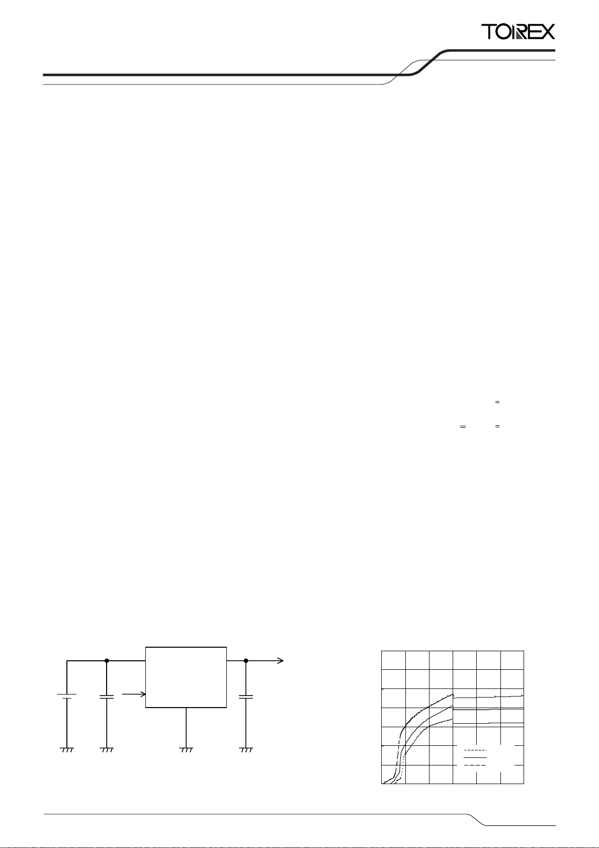
■TYPICAL APPLICATION CIRCUIT
●USP-4, SSOT-24, SOT-25,USPN-4 packages
(For the USP-3 package, with no CE pin)
VIN VOUT
CE
VSS
CIN=1.0uF
VOUT
CL=0.1uF
(ceramic)
(ceramic)
■FEATURES
Maximum Output Current : 200mA (300mA Limit, TYP.)
@ V
Dropout Voltage : 320mV @ I
@ V
OUT=3.0V, VIN=4.0V
OUT = 100mA
OUT = 3.0V
Operating Input V olta ge : 1.5V ~ 6.0V
Output Voltage Range :
0.9V ~ 5.0V (0.1V Increments)
Highly Accurate : Set voltage accuracy ±2%
(1.5V<V
OUT(T)<5.0V)
Set voltage accuracy ±30mV
(0.9V<
VOUT(T)<1.5V)
Low Power Consumption : 0.8μA (TYP.)
Stand-by Current : Less than 0.1μA
Operating Temperature Range : - 40℃~ 85℃
Low ESR Capacitor Compatible : Ceramic capacitor
Current Limiter Circuit Built-In
Packages : USP-4
SSOT-24
U S P-3 ( For the XC6215P series only)
SOT-25
USPN-4
Environmentally Friendly
: EU RoHS Compliant, Pb Free
■TYPICAL PERFORMANCE
CHARACTERISTICS
●Supply Current vs. Input Voltage
1.4
1.2
1.0
(μA)
SS
0.8
0.6
0.4
Supply Current I
0.2
XC6215x302
CIN=1.0μF(ceramic),CL=0.1μF(ceram ic)
VIN=VCE
Ta=-40
℃
Ta=25
℃
Ta=85
℃
0.0
0123456
Input Voltage VIN (V)
1/36

r
XC6215 Series
■PIN CONFIGURATION
USPN-4
(BOTTOM VIEW)
* For mounting intensity and heat dissipation,
please refer to recommended mounting pattern
and recommended metal mask when soldering
the pad of USP-4. Mounting should be
electrically isolated or connected to
the V
SS (No.2) pin.
■PIN ASSIGNMENT
VOUT
VIN
USP-3
(BOTTOM VIEW)
PIN NUMBER
USPN-4 USP-3 USP-4 SSOT-24 SOT-25
4
2
3
1
-
■PRODUCT CLASSIFICATION
●Ordering Information
XC6215①②③④⑤⑥-⑦
1
3
-
2
-
(*1)
DESIGNATOR DESCRIPTION SYMBOL DESCRIPTION
① Type of Regulator
②③ Output Voltage 09 ~ 50
④ Output Voltage Accuracy 2
Packages
⑤⑥-⑦
(*1)
The “-G” suffix indicates that the products are Halogen and Antimony free as well as being fully EU RoHS compliant.
(*2)
The device orientation is fixed in its embossed tape pocket. For reverse orientation, please contact your local Torex sales office o
representative. (Standard orientation: ⑤R-⑦, Reverse orientation: ⑤L-⑦)
Taping Type
VSS
3
2
1
3
VSS
USP-4
(BOTTOM VIEW)
SSOT-24
(TOP VIEW)
(TOP VIEW)
PIN NAME FUNCTION
4
2
3
1
-
4 1 VIN Power Supply
2 2 VSS Ground
1 3 CE ON / Off Switch
3 5 VOUT Output
- 4 NC No Connection
B CE logic = High active with no pull-down resistor
P 3 pin regulator with no CE pin (USP-3 only)
0.9 V ~ 5.0V, 0.1V step
e.g. V
OUT=3.0V②=3, ③=0
+
2 % accuracy
e.g. V
OUT=3.0V②=3, ③=0, ④=2
GR-G USP-4
NR SSOT-24
NR-G SSOT-24
MR SOT-25
(*2)
MR-G SOT-25
HR USP-3 (for the XC6215P series only)
HR-G USP-3 (for the XC6215P series only)
7R-G USPN-4
SOT-25
2/36
A
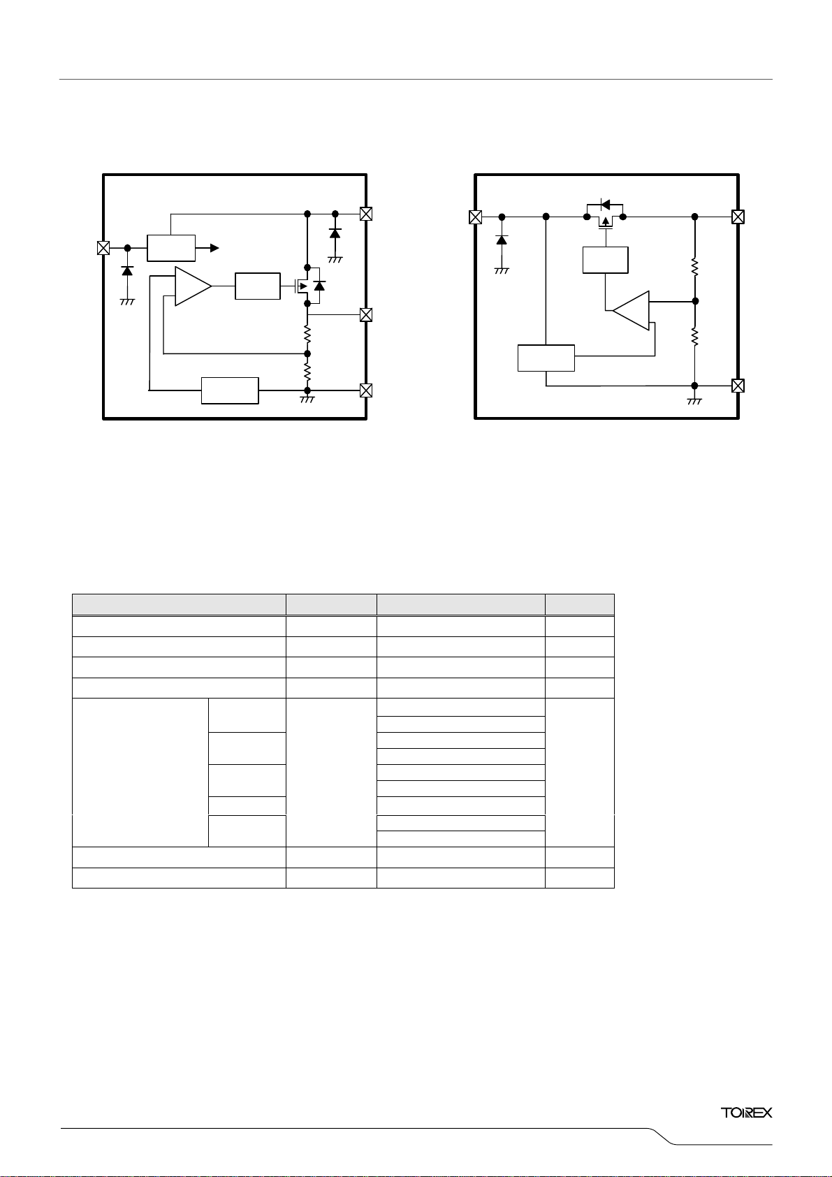
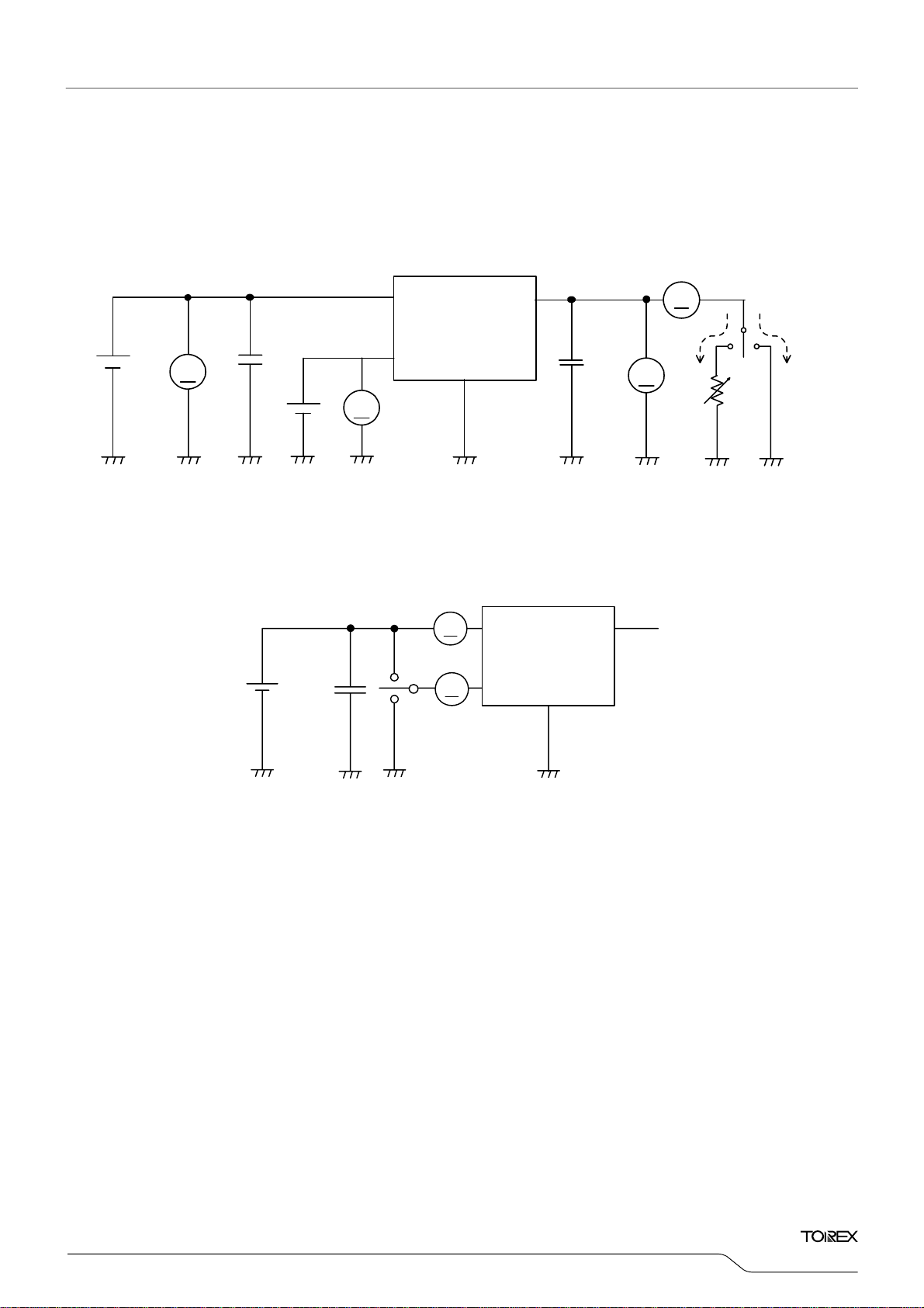
■BLOCK DIAGRAMS
●XC6215B Series ●XC6215P Series
CE
■
BSOLUTE MAXIMUM RATINGS
ON/OFF
Control
Error
Amp
+
each circuit
Current
Limit
R1
R2
Voltage
Reference
* Diodes shown in the above circuit are ESD protection diodes and parasitic diodes
V
V
V
IN
OUT
SS
V
IN
Voltage
Reference
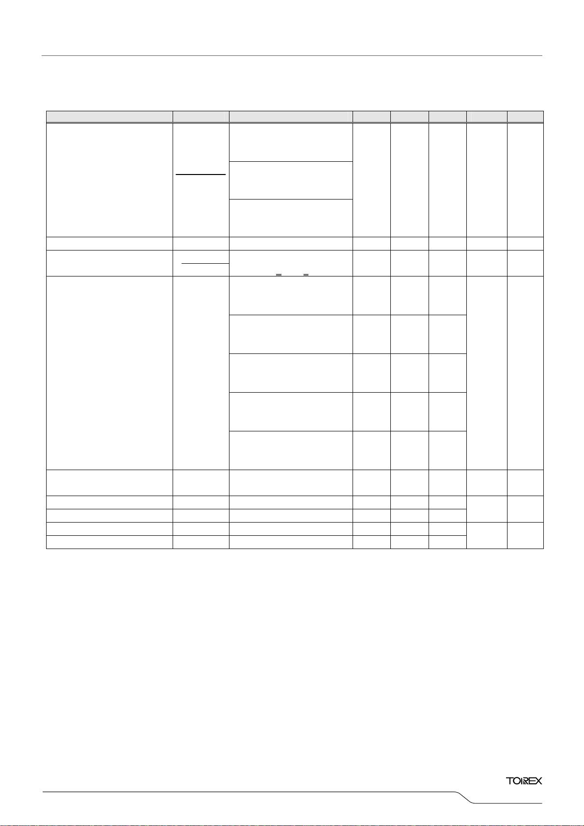
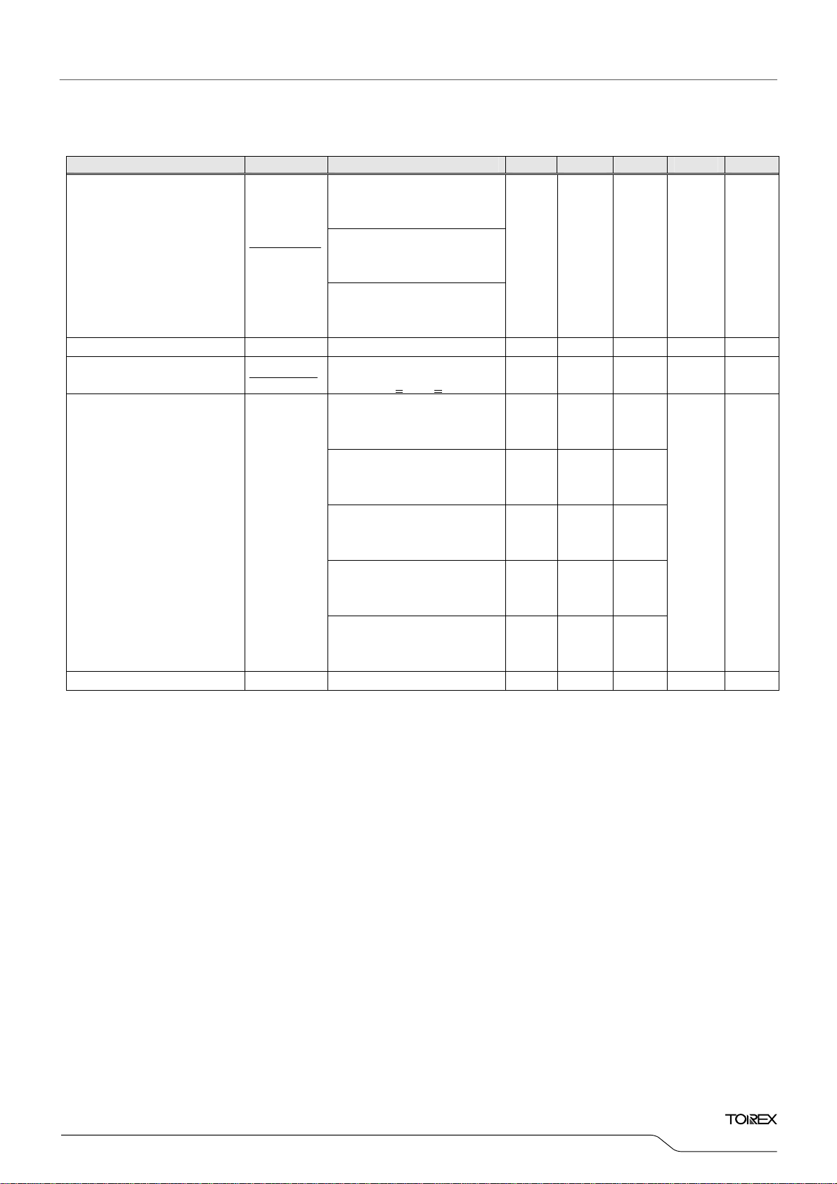
PAR AMETER SYMBOL RATINGS UNITS
Input Voltage VIN - 0.3 ~ + 7.0 V
Output Current IOUT 500 (*1) mA
Output Voltage VOUT VSS - 0.3 ~ VIN + 0.3 V
CE Input Voltage (*2) VCE VSS - 0.3 ~ + 7.0 V
250
150
120
120
100
Power Dissipation
SOT-25
SSOT-24
USP-4
USP-3
USPN-4
600(PCB mounted)(*3)
500(PCB mounted)(*3)
Pd
1000(PCB mounted)(*3)
600(PCB mounted)(*3)
Operating Temperature Range Topr - 40 ~ + 85
Storage Temperature Range Tstg - 55 ~ +125
Note:
*1: IOUT = Pd/ (VIN-VOUT)
*2: Except for the XC6215P series
*3: The power dissipation figure shown is PCB mounted. Please refer to pages 33 to 35 for details.
mW
℃
℃
Current
Limit
Error
Amp
XC6215
Series
V
OUT
R1
+
-
R2
V
SS
3/36

XC6215 Series
■ELECTRICAL CHARACTERISTICS
●XC6215B Series
PAR AMETER SYMBOL CONDITIONS MIN. TYP. MAX. UNIT.
Output Voltage (*2) VOUT(E)
Maximum Output Current IOUTMAX
Load Regulation VOUT
Dropout Voltage (*3) Vdif
Supply Current IDD
Stand-by Current Istby
VIN=VCE=VOUT(T) (*1) + 1.0V,
OUT=1mA
I
VIN=VCE=VOUT(T) + 1.0V
VOUT(T)=0.9V
VIN=VCE=VOUT(T) + 1.0V
OUT(T)=1.0V ~ 1.1V
V
VIN=VCE=VOUT(T) + 1.0V V
OUT(T)=1.2V ~ 1.3V
V
VIN=VCE=VOUT(T) + 1.0V
VOUT(T)=1.4V ~ 1.6V
VIN=VCE=VOUT(T) + 1.0V
OUT(T)=1.7V ~ 2.2V
V
VIN=VCE=VOUT(T) + 1.0V
OUT(T)=2.3V ~ 2.9V
V
VIN=VCE=VOUT(T) + 1.0V
VOUT(T)≧3.0V
VIN=VCE=VOUT(T) + 1.0V
OUT(T)=0.9V
V
1mA≦I
VIN=VCE=VOUT(T) + 1.0V
VOUT(T)= 1.0V ~ 1.1V
1mA≦I
VIN=VCE=VOUT(T) + 1.0V
OUT(T)=1.2V~1.3V
V
1mA≦IOUT≦80mA
IN=VCE=VOUT(T) + 1.0V
V
OUT(T)≧1.4V
V
1mA≦I
VCE=VIN, VOUT(T)=0.9V
IOUT=50mA
VCE=VIN, VOUT(T)=1.0V ~ 1.1V
OUT=60mA
I
VCE=VIN, VOUT(T)=1.2V ~ 1.3V
OUT=80mA
I
CE=VIN, VOUT(T)≧1.4V
V
IOUT=100mA
VIN=VCE=VOUT(T) + 1.0V
OUT(T)≦3.9V
V
VIN=VCE=VOUT(T) + 1.0V
OUT(T)≧4.0V
V
VIN=VOUT(T) + 1.0V,
VCE=VSS
OUT≦50mA
OUT≦60mA
OUT≦100mA
Ta = 2 5 ℃
CIRCUIT
E-0(*6) V ①
50 70 -
60 80 -
80 110 -
100 140 -
mA ①
120 150 -
150 195 -
200 300 -
- 15 70 mV 1
E-1(*6) mV 1
- 0.8 1.5
μA 2
- 1.0 1.8
- 0.01 0.10 μA 2
4/36
A
■ELECTRICAL CHAR
●XC6215B Series (Continued)
CTERISTICS (Continued)
PAR AMETER SYMBOL CONDITIONS MIN. TYP. MAX. UNIT.
VOUT(T)=0.9V, VCE=VIN
1.5V≦V
IN≦6.0V
OUT=1mA
I
VOUT(T)=1.0V~1.2V, VCE=VIN
VOUT(T)+0.5V≦VIN≦6.0V
OUT=1mA
I
OUT(T)≧1.3V, VCE=VIN
V
V
OUT(T)+0.5V≦VIN≦6.0V
OUT=30mA
I
- 0.05 0.15 %/V ①
Line Regulation
V
V
OUT
IN z VOUT
Input Voltage VIN - 1.5 - 6.0 V -
Output Voltage
Temperature Characteristics
VOUT
Topr
z VOUT
V
IN=VCE=VOUT(T)+1.0V, IOUT =30mA
- 40℃<
Topr < 85℃
- ±100 -
VOUT=VOUT(E)×0.95
OUT(T)=0.9V
V
V
IN=VCE= VOUT(T)+2.0V
100 300 -
VOUT=VOUT(E)×0.95
OUT(T)=1.0V ~ 1.1V
V
120 300 -
VIN=VCE= VOUT(T)+2.0V
VOUT=VOUT(E)×0.95
OUT(T)=1.2V ~ 1.3V
Current Limit IIim
V
V
IN=VCE= VOUT(T)+2.0V
160 300 -
VOUT=VOUT(E)×0.95
OUT(T)=1.4V ~ 2.9V
Short Circuit Current Ishort
V
V
IN=VCE= VOUT(T)+2.0V
V
OUT=VOUT(E)×0.95
V
OUT(T)≧3.0V
V
IN=VCE= VOUT(T)+1.0V
VIN=VCE=VOUT(T)+1.0V,
OUT=0V
V
200 300 -
200 300 -
- 50 - mA ①
CE ‘H’ Level Voltage VCEH VIN=VOUT(T)+1.0V 1.0 - 6.0
CE ‘L’ Level Voltage VCEL VIN=VOUT(T)+1.0V - - 0.3
CE ‘H’ Level Current ICEH VIN=VCE=VOUT(T)+1.0V - 0.1 - 0.1
CE ‘L’ Level Current ICEL VIN=VOUT(T)+1.0V, VCE=VSS - 0.1 - 0.1
NOTE:
OUT(T): Fixed output voltage
*1: V
OUT(E) = Effective output voltage
*2: V
(i.e. the output voltage when “V
*3: Vdif = { V
IN1 = The input voltage when VOUT1 appears as input voltage is gradually decreased.
*4: V
OUT1 = A voltage equal to 98% of the output voltage whenever an amply stabilized IOUT { VOUT(T) + 1.0V } is input.
*5: V
*6: Refer to “VOLTAGE CHART”.
IN1
(*4)–
VOUT1
(*5)
OUT(T) + 1.0V” is provided at the VIN pin while maintaining a certain IOUT value).
}
XC6215
Series
Ta = 2 5 ℃
CIRCUIT
ppm /
℃
mA ①
V ①
μA ②
①
5/36
XC6215 Series
■ELECTRICAL CHARACTERISTICS (Continued)
●XC6215P Series
PAR AMETER SYMBOL CONDITIONS MIN. TYP. MAX. UNIT.
Output Voltage (*2) VOUT(E)
Maximum Output Current IOUTMAX
Load Regulation VOUT
Dropout Voltage (*3) Vdif
Supply Current IDD
6/36
VIN=VOUT(T) (*1) + 1.0V,
OUT=1mA
I
VIN=VOUT(T) + 1.0V
VOUT(T)=0.9V
VIN=VOUT(T) + 1.0V
OUT(T)=1.0V ~ 1.1V
V
VIN=VOUT(T) + 1.0V
OUT(T)=1.2V ~ 1.3V
V
VIN=VOUT(T) + 1.0V
VOUT(T)=1.4V ~ 1.6V
VIN=VOUT(T) + 1.0V
OUT(T)=1.7V ~ 2.2V
V
VIN=VOUT(T) + 1.0V
OUT(T)=2.3V ~ 2.9V
V
VIN=VOUT(T) + 1.0V
VOUT(T)≧3.0V
VIN=VOUT(T) + 1.0V
OUT(T)=0.9V
V
1mA≦I
OUT≦50mA
VIN=VOUT(T) + 1.0V
VOUT(T)= 1.0V~1.1V
1mA≦I
OUT≦60mA
VIN=VOUT(T) + 1.0V
OUT(T)=1.2V~1.3V
V
1mA≦IOUT≦80mA
IN=VOUT(T) + 1.0V
V
OUT(T)≧1.4V
V
1mA≦I
OUT≦100mA
VOUT(T)=0.9V
IOUT=50mA
VOUT(T)=1.0V ~ 1.1V
OUT=60mA
I
VOUT(T)=1.2V ~ 1.3V
OUT=80mA
I
OUT(T)≧1.4V
V
IOUT=100mA
VIN=VOUT(T)=1.0V
OUT(T)≦3.9V
V
VIN= VOUT(T)+1.0V
OUT(T)≧4.0V
V
Ta = 2 5 ℃
CIRCUIT
E-0 (*6) V ①
50 70 -
60 80 -
80 110 -
100 140 -
mA ①
120 150 -
150 195 -
200 300 -
- 15 70 mV 1
E-1 (*6) mV 1
- 0.8 1.5
μA 2
- 1.0 1.8
A
■ELECTRIC
●XC6215P Series (Continued)
L CHARACTERISTICS (Continued)
PAR AMETER SYMBOL CONDITIONS MIN. TYP. MAX. UNIT.
VOUT(T)=0.9V
1.5V≦V
IN≦6.0V
OUT=1mA
I
VOUT(T)=1.0V~1.2V
VOUT(T)+0.5V≦VIN≦6.0V
OUT=1mA
I
OUT(T)≧1.3V
V
V
OUT(T)+0.5V≦VIN≦6.0V
OUT=30mA
I
- 0.05 0.15 %/V ①
Line Regulation
V
V
OUT
IN z VOUT
Input Voltage VIN - 1.5 - 6.0 V -
Output Voltage
Temperature Characteristics
VOUT
Topr
z VOUT
V
IN=VOUT(T)+1.0V, IOUT= 30mA
- 40℃<
Topr < 85℃
- ±100 -
ppm /℃ ①
VOUT=VOUT(E)×0.95
OUT(T)=0.9V
V
V
IN= VOUT(T)+2.0V
100 300 -
VOUT=VOUT(E)×0.95
OUT(T)=1.0V ~ 1.1V
V
120 300 -
VIN=VOUT(T)+2.0V
VOUT=VOUT(E)×0.95
OUT(T)=1.2V ~ 1.3V
Current Limit IIim
V
V
IN=VOUT(T)+2.0V
160 300 -
VOUT=VOUT(E)×0.95
OUT(T)=1.4V ~ 2.9V
V
V
IN=VOUT(T)+2.0V
V
OUT=VOUT(E)×0.95
V
OUT(T)≧3.0V
V
IN=VOUT(T)+1.0V
200 300 -
200 300 -
Short Circuit Current Ishort VIN=VOUT(T)+1.0V, VOUT=0V - 50 - mA ①
NOTE:
*1: V
OUT(T): Fixed output voltage
OUT(E) = Effective output voltage
*2: V
(i.e. the output voltage when “V
*3: Vdif = { V
IN1 = The input voltage when VOUT1 appears as input voltage is gradually decreased.
*4: V
OUT1 = A voltage equal to 98% of the output voltage whenever an amply stabilized IOUT { VOUT(T) + 1.0V } is input.
*5: V
*6: Refer to “VOLTAGE CHART”.
IN1
(*4)
– VOUT1
(*5)
OUT(T) + 1.0V” is provided at the VIN pin while maintaining a certain IOUT value).
}
XC6215
Series
Ta = 2 5 ℃
CIRCUIT
mA ①
7/36
XC6215 Series
■VOLTAGE CHART
●Dropout Voltage Chart
SETTING OUTPUT
VOLTAGE
VOUT(T)
0.9
1.0
1.1
1.2
1.3
1.4
1.5
1.6
1.7
1.8
1.9
2.0
2.1
2.2
2.3
2.4
2.5
2.6
2.7
2.8
2.9
3.0
3.1
3.2
3.3
3.4
3.5
3.6
3.7
3.8
3.9
4.0
4.1
4.2
4.3
4.4
4.5
4.6
4.7
4.8
4.9
5.0
8/36
MIN. MAX. TYP. MAX.
0.870 0.930
0.970 1.030
1.070 1.130
1.170 1.230
1.270 1.330
1.370 1.430
1.470 1.530
1.568 1.632
1.666 1.734
1.764 1.836
1.862 1.938
1.960 2.040
2.058 2.142
2.156 2.244
2.254 2.346
2.352 2.448
2.450 2.550
2.548 2.652
2.646 2.754
2.744 2.856
2.842 2.958
2.940 3.060
3.038 3.162
3.136 3.264
3.234 3.366
3.332 3.468
3.430 3.570
3.528 3.672
3.626 3.774
3.724 3.876
3.822 3.978
3.920 4.080
4.018 4.182
4.116 4.284
4.214 4.386
4.312 4.488
4.410 4.590
4.508 4.692
4.606 4.794
4.704 4.896
4.802 4.998
4.900 5.100
E-0 E-1
OUTPUT VOLTAGE
(V)
VOUT Vdif
Ta = 2 5 ℃
DROPOUT VOLTAGE
(mV)
870 1000
860 1000
780 950
800 1000
720 900
750 960
700 890
680 860
650 830
630 800
610 780
580 740
580 740
580 740
510 650
510 650
450 580
450 580
450 580
450 580
450 580
320 420
320 420
320 420
320 420
320 420
320 420
320 420
320 420
320 420
320 420
290 380
290 380
290 380
290 380
290 380
290 380
290 380
290 380
290 380
290 380
230 310
■TEST CIRCUITS
●Circuit①
●Circuit ②
V
CIN=1.0uF
(ceramic)
CIN=1.0uF
(ceramic)
V
V
CE
IN
V
OUT
V
SS
VIN VOUT
A
CE
A
VSS
CL=0.1uF
(ceramic)
V
A
IOUT
OPEN
XC6215
Series
Ishort
RL
9/36
XC6215 Series
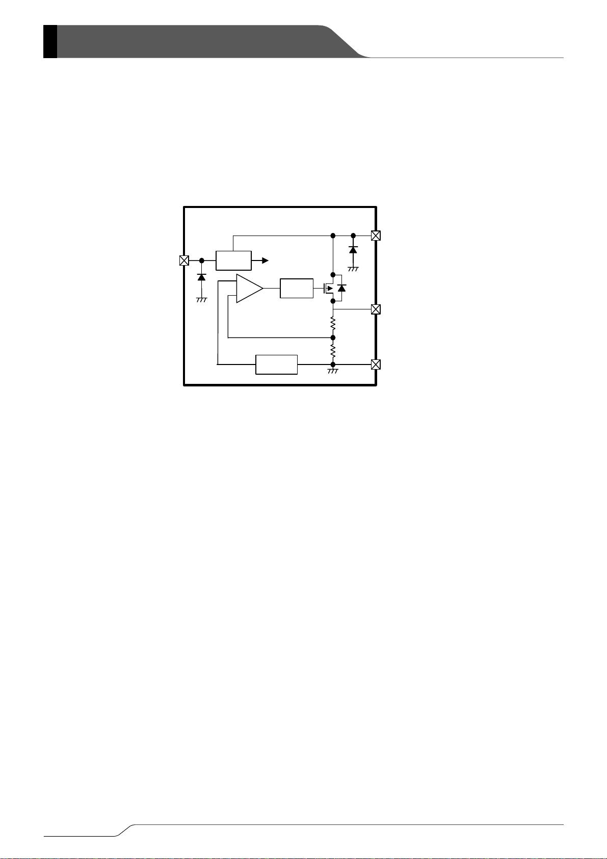
■OPERATIONAL EXPLANATION
●XC6215B Series (As for the XC6215P Series, with no CE pin)
<Output Voltage Control>
The voltage divided by resistors R1 & R2 is compared with the internal reference voltage by the error amplifier. The P-channel
MOSFET, which is connected to the V
is controlled and stabilized by a system of negative feedback. The current limit circuit and short protect circuit operate in relation
to the level of output current. Further, the IC's internal circuitry can be operated or shutdown via the CE pin's signal.
<Short Protection Circuit>
The XC6215 series’ regulator offers circuit protection by means of a built-in foldback circuit. When the load current reaches the
current limit level, the fixed current limiter circuit operates and output voltage drops. As a result of this drop in output voltage,
the foldback circuit operates, the output voltage drops further and output current decreases. When the output pin is shorted, a
current of about 50mA flows.
<CE Pin>
The IC's internal circuitry can be operated or shutdown via the signal from the CE pin with the XC6215B series. In shutdown
mode, output at the V
Active/No Pull-Down”, operations will become unstable with the CE pin open. We suggest that you use this IC with either a VIN
voltage or a V
fixed and the IC will operate normally. However, supply current may increase as a result of through current in the IC's internal
circuitry.
■NOTES ON USE
1. Please use this IC within the stated absolute maximum ratings. The IC is liable to malfunction should the ratings be exceeded.
2. Where wiring impedance is high, operations may become unstable due to noise and/or phase lag depending on output
current.
3. As for the XC6215 series, internally achieved phase compensation makes a stable operation of the IC possible even when
there is no output capacitor (C
about 0.1 to 1.0μF be connected between the VIN pin and the VSS pin. Moreover, during transient response, so as to prevent
an undershoot or overshoot, we recommend that the output capacitor (C
OUT pin and the VSS pin. However, please wire the input capacitor (CIN) and the output capacitor (CL) as close to the IC as
V
possible.
SS voltage input at the CE pin. If this IC is used with the correct specifications for the CE pin, the operational logic is
CE
OUT pin will be pulled down to the VSS level via R1 & R2. Note that the XC6215 series’ regulator is “High
10/36
OUT pin, is then driven by the subsequent output signal. The output voltage at the VOUT pin
V
IN
ON/OFF
Control
L). In order to stabilize the VIN’s voltage level, we recommend that an input capacitor (CIN) of
-
+
Error
Amp
each circuit
Voltage
Reference
Current
Limit
V
OUT
R1
R2
V
SS
L) of about 0.1 to1.0μF be connected between the
■TYPICAL PERFORMANCE CHARACTERISTICS
(1) Output Voltage vs. Output Current
1.2
0.9
(V)
OUT
0.6
0.3
Output Voltage V
0.0
0 50 100 150 200 250 300 350
1.8
1.5
(V)
1.2
OUT
0.9
0.6
Output Voltage V
0.3
0.0
0 50 100 150 200 250 300 350
3.5
3.0
(V)
2.5
OUT
2.0
1.5
1.0
Output Voltage V
0.5
0.0
0 50 100 150 200 250 300 350
XC6215x092
CIN=1.0μ F(ceramic),CL=0 .1μ F(ceram ic)
Output Current I
(mA )
OUT
VIN=VCE=1.9V
Ta=-40
℃
Ta=25
℃
Ta=85
℃
XC6215x152
CIN=1.0μ F(ceramic),CL=0 .1μ F(ceram ic)
Output Current I
(mA )
OUT
VIN=VCE=2.5V
Ta=-40
℃
Ta=25
℃
Ta=85
℃
XC6215x302
CIN=1.0μ F(ceramic),CL=0 .1μ F(ceram ic)
Output Current I
(mA )
OUT
VIN=VCE=4.0V
Ta=-40
℃
Ta=25
℃
Ta=85
℃
1.2
0.9
(V)
OUT
0.6
0.3
Output Voltage V
0.0
0 50 100 150 200 250 300 350
1.8
1.5
(V)
1.2
OUT
0.9
0.6
Output Voltage V
0.3
0.0
0 50 100 150 200 250 300 350
3.5
3.0
(V)
2.5
OUT
2.0
1.5
1.0
Output Voltage V
0.5
0.0
0 50 100 150 200 250 300 350
XC6215
XC6215x092
CIN=1.0μ F(ceramic),CL=0 .1μ F(ceram ic)
Output Current I
XC6215x152
CIN=1.0μ F(ceramic),CL=0 .1μ F(ceram ic)
Output Current I
XC6215x302
CIN=1.0μ F(ceramic),CL=0 .1μ F(ceram ic)
Output Current I
(mA )
OUT
OUT
(mA )
OUT
Ta =25
VIN=1.5V
VIN=1.9V
VIN=2.4V
VIN=2.9V
Ta =25
VIN=1.8V
VIN=2.0V
VIN=2.5V
VIN=3.0V
(mA )
Ta =25
VIN=3.3V
VIN=3.5V
VIN=4.0V
VIN=4.5V
Series
℃
℃
℃
11/36
A
XC6215 Series
■TYPIC
(1) Output Voltage vs. Output Current (Continued)
6.0
5.0
(V)
4.0
OUT
3.0
2.0
Output Voltage V
1.0
0.0
0 50 100 150 200 250 300 350
(2) Output Voltage vs. Input Voltage
1.3
1.1
(V)
OUT
0.9
0.7
Output Voltage V
0.5
0.3
0.5 1 1.5 2 2.5
1.9
1.7
(V)
OUT
1.5
1.3
Output Voltage V
1.1
0.9
0.5 1 1.5 2 2.5
12/36
L PERFORMANCE CHARACTERISTICS (Continued)
XC6215x502
CIN=1.0μ F(ceramic),CL=0 .1μ F(ceram ic)
Output Current I
XC6215x092
VIN=VCE
CIN=1.0μ F(ceramic),CL=0 .1μ F(ceram ic)
Input Voltage V
XC6215x152
CIN=1.0μ F(ceramic),CL=0 .1μ F(ceram ic)
Input Voltage V
VIN=VCE=6.0V
Ta=-40
(mA )
OUT
IOUT= 1m A
IOUT=30mA
IOUT=50mA
(V)
IN
VIN=VCE
IOUT= 1m A
IOUT=30mA
IOUT=50mA
IOUT=100mA
(V)
IN
Ta=25
Ta=85
XC6215x502
CIN=1.0μ F(ceramic),CL=0 .1μ F(ceram ic)
Ta =25
℃
6.0
5.0
(V)
4.0
OUT
3.0
2.0
℃
℃
℃
Output Voltage V
1.0
VIN=5.3V
VIN=5.5V
VIN=6.0V
0.0
0 50 100 150 200 250 300 350
Output Current I
OUT
(mA )
XC6215x092
VIN=VCE
CIN=1.0μ F(ceramic),CL=0 .1μ F(ceram ic)
0.95
IOUT= 1m A
IOUT=30mA
IOUT=50mA
(V)
OUT
0.90
Output Voltage V
0.85
2 2.5 3 3.5 4 4.5 5 5.5 6
Input Voltage V
(V)
IN
XC6215x152
CIN=1. 0μ F(ceramic),CL=0 .1μ F(ceram ic)
VIN=VCE
1.55
IOUT= 1m A
IOUT=30mA
IOUT=50mA
(V)
OUT
IOUT=100mA
1.50
Output Voltage V
1.45
2.5 3 3.5 4 4.5 5 5.5 6
Input Voltage V
(V)
IN

■TYPICAL PERFORMANCE CHARACTERISTICS (Continued)
(2) Output Voltage vs. Input Voltage (Continued)
3.4
3.2
(V)
OUT
3.0
2.8
Output Voltage V
2.6
XC6215x302
VIN=VCE
CIN=1.0μ F(ceramic),CL=0 .1μ F(ceram ic)
IOUT= 1m A
IOUT=30mA
IOUT=50mA
IOUT=100mA
3.05
(V)
OUT
3.00
Output Voltage V
2.4
22.533.54
Input Voltage V
(V)
IN
XC6215x502
CIN=1.0μ F(ceramic),CL=0 .1μ F(ceram ic)
VIN=VCE
5.4
IOUT= 1m A
IOUT=30mA
5.2
(V)
OUT
5.0
IOUT=50mA
IOUT=100mA
4.8
2.95
3.5 4 4.5 5 5.5 6
5.05
(V)
OUT
5.00
Output V oltage V
4.6
Output V oltage V
4.4
4 4.5 5 5.5 6
Input Voltage V
(V)
IN
4.95
5.5 5.6 5.7 5.8 5.9 6
XC6215x302
CIN=1. 0μ F(ceramic),CL=0 .1μ F(ceram ic)
Input Voltage V
XC6215x502
CIN=1.0μ F(ceramic),CL=0 .1μ F(ceram ic)
Input Voltage V
(3) Dropout Voltage vs. Output Current
1
0.9
0.8
0.7
0.6
0.5
0.4
0.3
Dropout Voltage Vdif (V)
0.2
0.1
0
0 1020304050
XC6215x092
VIN=VCE
CIN=1.0μ F(ceramic),CL=0 .1μ F(ceram ic)
Minimum Operating Voltage
Ta=-40
Ta=25
Ta=85
Output Current IOUT (mA)
XC6215x152
VIN=VCE
1
CIN=1.0μ F(ceramic),CL=0 .1μ F(ceram ic)
0.9
0.8
0.7
0.6
0.5
0.4
℃
℃
℃
0.3
Dropout Voltage Vdif (V)
0.2
0.1
0
0 20406080100
Output Current IOUT (mA)
VIN=VCE
IOUT= 1m A
IOUT=30mA
IOUT=50mA
IOUT=100mA
(V)
IN
VIN=VCE
IOUT= 1m A
IOUT=30mA
IOUT=50mA
IOUT=100mA
(V)
IN
XC6215
Series
Ta=-40
℃
Ta=25
℃
Ta=85
℃
13/36

XC6215 Series
■TYPICAL PERFORMANCE CHARACTERISTICS (Continued)
(3) Dropout Voltage vs. Output Current (Continued)
1
0.9
0.8
0.7
0.6
0.5
0.4
0.3
Dropout Voltage Vdif (V)
0.2
0.1
0
0 50 100 150 200
(4) Supply Current vs. Input Voltage
1.4
1.2
1.0
(μA)
SS
0.8
0.6
0.4
Supply Current I
0.2
0.0
0123456
1.4
1.2
(μA)
SS
Supply Current I
1.0
0.8
0.6
0.4
0.2
0.0
0123456
14/36
XC6215x302
VIN=VCE
CIN=1.0μ F(ceramic),CL=0 .1μ F(ceram ic)
Ta=-40
℃
Ta=25
℃
Ta=85
℃
Output Current IOUT (mA)
XC6215x092
VIN=VCE
CIN=1.0μ F(ceramic),CL=0 .1μ F(ceram ic)
Ta=-40
℃
Ta=25
℃
Ta=85
℃
Input Voltage V
(V)
IN
XC6215x302
CIN=1.0μ F(ceramic),CL=0 .1μ F(ceram ic)
VIN=VCE
Ta=-40
℃
Ta=25
℃
Ta=85
℃
Input Voltage V IN (V)
SS
XC6215x502
VIN=VCE
1
CIN=1.0μ F(ceramic),CL=0 .1μ F(ceram ic)
0.9
Ta=-40
0.8
0.7
Ta=25
Ta=85
℃
℃
℃
0.6
0.5
0.4
0.3
Dropout Voltage Vdif (V)
0.2
0.1
0
0 50 100 150 200
Output Current IOUT (mA)
XC6215x152
CIN=1.0μ F(ceramic),CL=0 .1μ F(ceram ic)
1.4
1.2
1.0
(μA)
0.8
0.6
0.4
Supply Current I
0.2
0.0
0123456
Input Voltage V IN (V)
XC6215x502
1.4
CIN=1.0μ F(ceramic),CL=0 .1μ F(ceram ic)
1.2
1.0
(μA)
SS
0.8
0.6
0.4
Supply Current I
0.2
0.0
0123456
Input Voltage V IN (V)
VIN=VCE
Ta=-40
℃
Ta=25
℃
Ta=85
℃
VIN=VCE
Ta=-40
℃
Ta=25
℃
Ta=85
℃

p
(
)
■TYPICAL PERFORMANCE CHARACTERISTICS (Continued)
(5) Output Voltage vs. Ambient Temperature
1.00
(V)
OUT
0.90
XC6215x092
VIN=VCE=1 .9V
CIN=1. 0μ F(ceramic),CL=0 .1μ F(ceram ic)
IOUT= 1m A
IOUT=30mA
IOUT=50mA
XC6215x152
VIN=VCE=2 .5V
CIN=1.0μ F(ceramic),CL=0 .1μ F(ceram ic)
1.65
IOUT= 1m A
IOUT=30mA
IOUT=50mA
(V)
OUT
1.50
Output V oltage V
Output V oltage V
0.80
-50 -25 0 25 50 75 100
Ambient Temperature Ta (
℃
XC6215x302
VIN=VCE=4 .0V
CIN=1.0μ F(ceramic),CL=0 .1μ F(ceram ic)
IOUT= 1m A
IOUT=30mA
IOUT=50mA
OUT
(V)
3.30
3.15
3.00
)
1.35
-50 -25 0 25 50 75 100
Ambient Temperature Ta (
XC6215x502
VIN=VCE=6 .0V
CIN=1.0μ F(ceramic),CL=0 .1μ F(ceram ic)
IOUT= 1m A
IOUT=30mA
IOUT=50mA
(V)
OUT
5.50
5.25
5.00
2.85
Output V oltage V
4.75
Output V oltage V
2.70
-50 -25 0 25 50 75 100
Ambient Temperature Ta (
)
℃
4.50
-50 -25 0 25 50 75 100
Ambient Temperature Ta (
(6) Supply Current vs. Ambient Temperature
1.5
XC6215x092
CIN=1.0μ F(ceramic),CL=0 .1μ F(ceram ic)
VIN=VCE=1.9V
1.5
1.2
(μA)
SS
0.9
(μA)
SS
1.2
0.9
0.6
Supply Current I
0.3
0.6
Supply Current I
0.3
0.0
-50 -25 0 25 50 75 100
Ambient Temperature Ta (
)
℃
0.0
-50 -25 0 25 50 75 100
XC6215x152
CIN=1.0μ F(ceramic),CL=0 .1μ F(ceram ic)
Ambient Tem
erature Ta
XC6215
Series
)
℃
)
℃
VIN=VCE=2.5V
℃
15/36

p
(
)
XC6215 Series
■TYPICAL PERFORMANCE CHARACTERISTICS (Continued)
(6) Supply Current vs. Ambient Temperature (Continued)
1.5
XC6215x302
CIN=1.0μ F(ceramic),CL=0 .1μ F(ceram ic)
VIN=VCE=4.0V
1.2
(μA)
SS
0.9
0.6
Supply Current I
0.3
0.0
-50 -25 0 25 50 75 100
Ambient Temperature Ta (℃)
(7) CE Threshold Voltage vs. Ambient Temperature
0.9
(V)
CEL
0.8
,V
CEH
0.7
0.6
CE Threshold Voltage V
0.5
-50 -25 0 25 50 75 100
0.9
(V)
CEL
0.8
,V
CEH
0.7
0.6
CE Threshold Voltage V
0.5
-50 -25 0 25 50 75 100
XC6215x092
VIN=1.9V , IOUT =1m A
CIN=1.0μ F(ceramic),CL=0 .1μ F(ceram ic)
High Level Voltage
Low Level Voltage
Ambient Temperature Ta (
)
℃
XC6215x302
VIN=4.0V , IOUT =1m A
CIN=1.0μ F(ceramic),CL=0 .1μ F(ceram ic)
High Level Voltage
Low Level Voltage
Ambient Temperature Ta (
)
℃
16/36
1.8
1.5
(μA)
1.2
SS
0.9
0.6
Supply Current I
0.3
0.0
-50 -25 0 25 50 75 100
0.9
(V)
CEL
0.8
,V
CEH
0.7
0.6
CE Threshold Voltage V
0.5
-50 -25 0 25 50 75 100
0.9
(V)
CEL
0.8
,V
CEH
0.7
0.6
CE Threshold Voltage V
0.5
-50 -25 0 25 50 75 100
XC6215x502
CIN=1.0μ F(ceramic),CL=0 .1μ F(ceram ic)
Ambient Tem
erature Ta
XC6215x152
VIN=2.5V , IOUT =1m A
CIN=1.0μ F(ceramic),CL=0 .1μ F(ceram ic)
Ambient Temperature Ta (
XC6215x502
VIN=6.0V , IOUT =1m A
CIN=1.0μ F(ceramic),CL=0 .1μ F(ceram ic)
Ambient Temperature Ta (
VIN=VCE=6.0V
℃
High Level Voltage
Low Level Voltage
)
℃
High Level Voltage
Low Level Voltage
)
℃

■TYPICAL PERFORMANCE CHARACTERISTICS (Continued)
(8) Input Transient Response
tr=tf=5μsec VIN=VCE ,
4
XC6215x092
IOUT =1 m A , CL =0 .1μ F(ceram ic)
XC6215x092
3.0
tr=tf=5μsec, VIN=VCE,
4
IOUT =1m A , CL =1.0 μF(ceram i c)
3
(V)
2
IN
Input Voltage
2.5
2.0
3
(V)
OUT
(V)
2
IN
Input Voltage
1
0
Input Voltage V
-1
Output Voltage
1.5
1.0
0.5
1
Output Voltage
0
Output Voltage V
Input Voltage V
-1
-2
Time (200μsec/div)
0.0
-2
Time (400μsec/div)
tr=tf=5μsec VIN=VCE ,
4
XC6215x092
IOUT =3 0m A , CL=0.1 μF(ceram ic)
3.0
XC6215x092
tr=tf=5μsec, VIN=VCE,
4
IOUT =3 0m A , CL= 1.0 μF(ceram ic)
3
(V)
2
IN
Input Voltage
2.5
2.0
3
(V)
OUT
(V)
2
IN
Input Voltage
1
0
Input Voltage V
-1
Output Voltage
1.5
1.0
0.5
1
Output Voltage
0
Output Voltage V
Input Voltage V
-1
-2
Time (200μsec/div)
0.0
-2
Time (200μsec/div)
tr=tf=5μsec VIN=VCE ,
4
XC6215x092
IOUT=50m A , CL=0.1μ F(cerami c)
3.0
tr=tf=5μsec, VIN=VCE,
4
XC6215x092
IOUT=50m A , CL=1.0μ F(cerami c)
3
2.5
3
(V)
2
IN
1
0
Input Voltage V
Input Voltage
Output Voltage
-1
2.0
1.5
1.0
0.5
(V)
OUT
(V)
2
IN
Input Voltage
1
Output Voltage
0
Input Voltage V
Output Voltage V
-1
-2
Time (200μsec/div)
0.0
-2
Time (200μsec/div)
XC6215
Series
3.0
2.5
2.0
1.5
1.0
0.5
0.0
3.0
2.5
2.0
1.5
1.0
0.5
0.0
3.0
2.5
2.0
1.5
1.0
0.5
0.0
17/36
(V)
OUT
Output Voltage V
(V)
OUT
Output Voltage V
(V)
OUT
Output Voltage V

XC6215 Series
■TYPICAL PERFORMANCE CHARACTERISTICS (Continued)
(8) Input Transient Response (Continued)
tr=tf=5μsec VIN=VCE ,
4.5
3.5
(V)
2.5
IN
1.5
0.5
Input Volt age V
-0.5
-1.5
tr=tf=5μsec VIN=VCE ,
4.5
3.5
(V)
2.5
IN
1.5
0.5
Input Volt age V
-0.5
-1.5
tr=tf=5μsec, VIN=VCE,
4.5
3.5
(V)
2.5
IN
1.5
0.5
Input Volt age V
-0.5
-1.5
18/36
XC6215x152
IOUT=1m A , CL=0 .1μ F(ceramic)
Input V olt a ge
Output Voltage
Time (400μsec/div)
XC6215x152
IOUT=30m A , CL=0.1μ F(ceram ic)
Input V olt a ge
Output Voltage
Time (400μsec/div)
XC6215x152
IOUT=100 mA , CL=0.1 μF(ceram i c)
Input V olt age
Output Voltage
Time (400μsec/div)
3.5
3.0
2.5
2.0
1.5
1.0
0.5
3.5
3.0
2.5
2.0
1.5
1.0
0.5
3.5
3.0
2.5
2.0
1.5
1.0
0.5
(V)
OUT
Output Voltage V
(V)
OUT
Output Voltage V
(V)
OUT
Output Voltage V
XC6215x152
tr=tf=5μsec, VIN=VCE,
4.5
IOUT=1m A , CL=1 .0μ F(
3.5
(V)
2.5
IN
Input V olt age
1.5
Output Voltage
0.5
Input Volt age V
-0.5
-1.5
Tim e (400μsec/div)
XC6215x152
tr=tf=5μsec, VIN=VCE,
IOUT= 30m A , CL=1.0μ F(ceram ic)
4.5
3.5
(V)
2.5
IN
Input V olt age
1.5
Output Voltage
0.5
Input Voltage V
-0.5
-1.5
Time (400μsec/div)
XC6215x152
tr=tf=5μsec, VIN=VCE,
IOUT= 100 mA , CL=1.0 μF(ceram i c)
4.5
3.5
(V)
2.5
IN
Input V olt age
1.5
Output Voltage
0.5
Input Volt age V
-0.5
-1.5
Tim e (400μsec/div)
セラミック
)
3.5
3.0
2.5
2.0
1.5
1.0
0.5
3.5
3.0
2.5
2.0
1.5
1.0
0.5
3.5
3.0
2.5
2.0
1.5
1.0
0.5
(V)
OUT
Output Voltage V
(V)
OUT
Output Voltage V
(V)
OUT
Output Voltage V

■TYPICAL PERFORMANCE CHARACTERISTICS (Continued)
(8) Input Transient Response (Continued)
tr=tf=5μsec VIN=VCE ,
6
XC6215x302
IOUT=1m A , CL=0.1μF(ce ramic)
5.0
XC6215x302
tr=tf=5μsec, VIN=VCE,
6
IOUT= 1m A , CL=1 .0μ F(ceram ic)
5
(V)
IN
4
Input Voltage
4.5
4.0
5
(V)
OUT
(V)
4
IN
Input Voltage
3
Input Voltage V
2
Output Voltage
1
3.5
3.0
2.5
3
Output Voltage
2
Output V oltage V
Input Voltage V
1
0
Time (400μsec/div)
2.0
0
Tim e (4 00μsec/div)
tr=tf=5μsec, VIN=VCE ,
6
XC6215x302
IOUT=30m A , CL =0.1μF(ceram ic)
5.0
tr=tf=5μsec, VIN=VCE,
6
XC6215x302
IOUT=30m A , CL =1.0μF(ceram ic)
5
(V)
4
IN
3
2
Input Voltage V
1
0
Input Voltage
Output Voltage
Tim e (40 0μsec/div)
4.5
4.0
3.5
3.0
2.5
2.0
(V)
OUT
Output V oltage V
5
(V)
4
IN
Input Voltage
3
Output Voltage
2
Input Voltage V
1
0
Tim e (40 0μsec/div)
tr=tf=5μsec VIN=VCE ,
6
XC6215x302
IOUT=100mA , CL=0.1μF(ceram ic)
5.0
XC6215x302
tr=tf=5μsec, VIN=VCE,
6
IOUT=100mA , CL=1.0μF(cerami c)
5
(V)
4
IN
3
2
Input Voltage V
1
Input Voltage
Output Voltage
4.5
4.0
3.5
3.0
2.5
(V)
OUT
Output V oltage V
(V)
IN
Input Voltage V
5
4
Input Voltage
3
Output Voltage
2
1
0
Tim e (4 00μsec/div)
2.0
0
Tim e (400μsec/div)
XC6215
Series
5.0
4.5
(V)
4.0
OUT
3.5
3.0
Output V oltage V
2.5
2.0
5.0
4.5
4.0
3.5
3.0
2.5
2.0
5.0
4.5
4.0
3.5
3.0
2.5
2.0
19/36
(V)
OUT
Output V oltage V
(V)
OUT
Output V oltage V

XC6215 Series
■TYPICAL PERFORMANCE CHARACTERISTICS (Continued)
(8) Input Transient Response (Continued)
tr=tf=5μsec, VIN=VCE,
7
6
(V)
5
IN
4
3
Input Voltage V
2
1
tr=tf=5μsec, VIN=VCE,
7
6
(V)
5
IN
4
3
Input Voltage V
2
1
tr=tf=5μsec, VIN=VCE,
7
6
(V)
5
IN
4
3
Input Voltage V
2
1
XC6215x502
IOUT =1m A , CL =0.1 μF(ceram ic)
Input Voltage
Output Voltage
Tim e (400μsec/div)
XC6215x502
IOUT =30 mA , CL=0 .1μ F(cerami c)
Input Voltage
Output Voltage
Tim e (4 00μsec/div)
XC6215x502
IOUT=100mA, CL=0.1μF(cerami c)
Input V olt ag e
Output Voltage
Tim e (4 00μsec/div)
20/36
XC6215x502
7.0
6.5
6.0
5.5
5.0
4.5
4.0
7.0
6.5
6.0
5.5
5.0
4.5
4.0
7.0
6.5
6.0
5.5
5.0
4.5
4.0
tr=tf=5μsec, VIN=VCE,
7
6
(V)
OUT
(V)
5
IN
4
3
Output V oltage V
Input Voltage V
2
1
tr=tf=5μsec, VIN=VCE,
7
6
(V)
OUT
(V)
5
IN
4
3
Output V oltage V
Input Voltage V
2
1
tr=tf=5μsec, VIN=VCE,
7
6
(V)
OUT
(V)
5
IN
4
3
Output V oltage V
Input Voltage V
2
1
IOUT=1 mA , CL=1.0 μF(ceram ic)
Input Voltage
Output Voltage
Time (400μsec/div)
XC6215x502
IOUT=30mA, CL=1.0μF(cerami c)
Input Voltage
Output Voltage
Tim e (400μsec/div)
XC6215x502
IOUT =1 0 0m A , CL=1 .0 μF(ceram i c)
Input Voltage
Output Voltage
Time (400μsec/div)
7.0
6.5
6.0
5.5
5.0
4.5
4.0
7.0
6.5
6.0
5.5
5.0
4.5
4.0
7.0
6.5
6.0
5.5
5.0
4.5
4.0
(V)
OUT
Output V oltage V
(V)
OUT
Output V oltage V
(V)
OUT
Output V oltage V

■TYPICAL PERFORMANCE CHARACTERISTICS (Continued)
(9) Load Transient Response
50
40
(mA )
30
OUT
20
Output Current I
10
0
50
40
(mA )
30
OUT
20
Output Current I
10
0
250
200
(mA )
150
OUT
100
Output Current I
50
0
XC6215x092
CIN=1 .0μ F(ceram ic),CL=0.1 μF(ceram ic)
tr=tf=5μsec, VIN=VCE=1.9V,
Output Voltage
Output Current
Tim e (200 μsec/div)
XC6215x152
CIN=1 .0μ F(ceram ic),CL=0.1 μF(ceram ic)
tr=tf=5μsec, VIN=VCE=2.5V,
Output Voltage
Output Current
Tim e (200 μsec/div)
XC6215x152
CIN=1 .0μ F(ceram ic),CL=0.1 μF(ceram ic)
tr=tf=5μsec, VIN=VCE=2.5V,
Output Voltage
Output Current
Tim e (2 00μsec/div)
1.5
1.0
0.5
0.0
-0.5
-1.0
2.0
1.5
1.0
0.5
0.0
-0.5
2.0
1.5
1.0
0.5
0.0
-0.5
(V)
OUT
Output Voltage V
(V)
OUT
Output Voltage V
(V)
OUT
Output Voltage V
(mA )
OUT
Output Current I
(mA )
OUT
Output Current I
50
40
30
20
10
50
40
(mA )
30
OUT
20
Output Current I
10
250
200
150
100
50
XC6215x092
CIN=1 .0μ F(ceram ic),CL=1.0 μF(ceram i c)
tr=tf=5μsec, VIN=VCE=1.9V,
Output Voltage
Output Current
0
Tim e (600μsec/div)
XC6215x152
CIN=1 .0μ F(ceram ic), CL= 1.0 μF(ceram ic)
tr=tf=5μsec, VIN=VCE=2.5V,
Output Voltage
Output Current
0
Time (400μsec/div)
XC 62 15 x 15 2
CIN=1 .0μ F(ceram ic), CL= 1.0 μF(ceram ic)
tr=tf=5μsec, VIN=VCE=2.5V,
Output Voltage
Output Current
0
Tim e (2 00μsec/div)
XC6215
Series
1.5
1.0
0.5
0.0
-0.5
-1.0
2.0
1.5
1.0
0.5
0.0
-0.5
2.0
1.5
1.0
0.5
0.0
-0.5
21/36
(V)
OUT
Output Voltage V
(V)
OUT
Output Voltage V
(V)
OUT
Output Voltage V

XC6215 Series
■TYPICAL PERFORMANCE CHARACTERISTICS (Continued)
(9) Load Transient Response (Continued)
50
40
(mA )
30
OUT
20
Output Current I
10
0
250
200
(mA)
150
OUT
100
Output Current I
50
50
40
(mA)
OUT
30
20
Output Current I
10
0
22/36
0
XC6215x302
tr=tf=5μsec, VIN=VCE=4.0V,
CIN=1. 0μ F(cerami c), CL=0.1 μF(cerami c)
Output Voltage
Output Current
Time (400μsec/div)
XC6215x302
tr=tf=5μsec, VIN=VCE=4.0V,
CIN=1.0μ F(cerami c), CL=0.1 μF(ce ram ic)
Output Voltage
Output Current
Tim e (6 00μsec/div)
XC6215x502
tr=tf=5μ sec, VIN=VCE=6.0V,
CIN=1 .0μ F(ceramic),CL=0.1μ F(cerami c)
Output Voltage
Output Current
Time (400μsec/div)
3.5
3.0
2.5
2.0
1.5
1.0
3.5
3.0
2.5
2.0
1.5
1.0
5.5
5.0
4.5
4.0
3.5
3.0
(V)
OUT
Output Voltage V
(V)
OUT
Output Voltage V
(V)
OUT
Output Voltage V
(mA )
OUT
Output Current I
(mA)
OUT
Output Current I
(mA)
OUT
Output Current I
50
40
30
20
10
0
250
200
150
100
50
40
30
20
10
XC6215x302
tr=tf=5μsec, VIN=VCE=4.0V,
CIN=1. 0μ F(ceramic),CL=1.0μF(ceramic)
Output V oltage
Output Current
Time (400μsec/div)
XC6215x302
tr=tf=5μsec, VIN=VCE=4.0V,
CIN=1 .0μ F(cerami c),CL=1.0 μF(ce ram ic)
Output Voltage
Output Current
50
0
Time (600μsec/div)
XC6215x502
tr=tf=5μsec, VIN=VCE=6.0V,
CIN=1 .0μ F(ceramic), CL=1 .0μ F(ceram ic)
Output Voltage
Output Current
0
Tim e (400μsec/div)
3.5
3.0
2.5
2.0
1.5
1.0
3.5
3.0
2.5
2.0
1.5
1.0
5.5
5.0
4.5
4.0
3.5
3.0
(V)
OUT
Output Voltage V
(V)
OUT
V
(V)
OUT
Output Voltage V

■TYPICAL PERFORMANCE CHARACTERISTICS (Continued)
(9) Load Transient Response (Continued)
250
XC6215x502
CIN=1. 0μ F(cerami c),CL=0.1μ F(ceramic)
tr=tf=5μ sec, VIN=VCE=6.0V,
5.5
250
XC6215x502
CIN=1.0μ F(cerami c),CL=1.0μ F(ceramic)
tr=tf=5μ sec, VIN=VCE=6.0V,
200
(mA )
150
OUT
Output Voltage
5.0
4.5
200
(V)
OUT
(mA )
OUT
Output V oltage
150
100
Output Current I
50
Output Current
4.0
3.5
Output Voltage V
Output Current I
100
Output Current
50
0
Tim e (4 00 μsec/div)
3.0
0
Tim e (400 μsec/div)
(10) Rising Response Time
tr=5μse c
VIN=VCE =0V→1.9V , IOUT =1m A , CL= 0.1μ F(ceram ic)
3
XC6215x092
tr=5μse c
6
VIN=VCE =0V→1.9V, IOUT=30mA , CL=0.1μF(cerami c)
3
2
1
Input Voltage
0
5
(V)
4
OUT
3
2
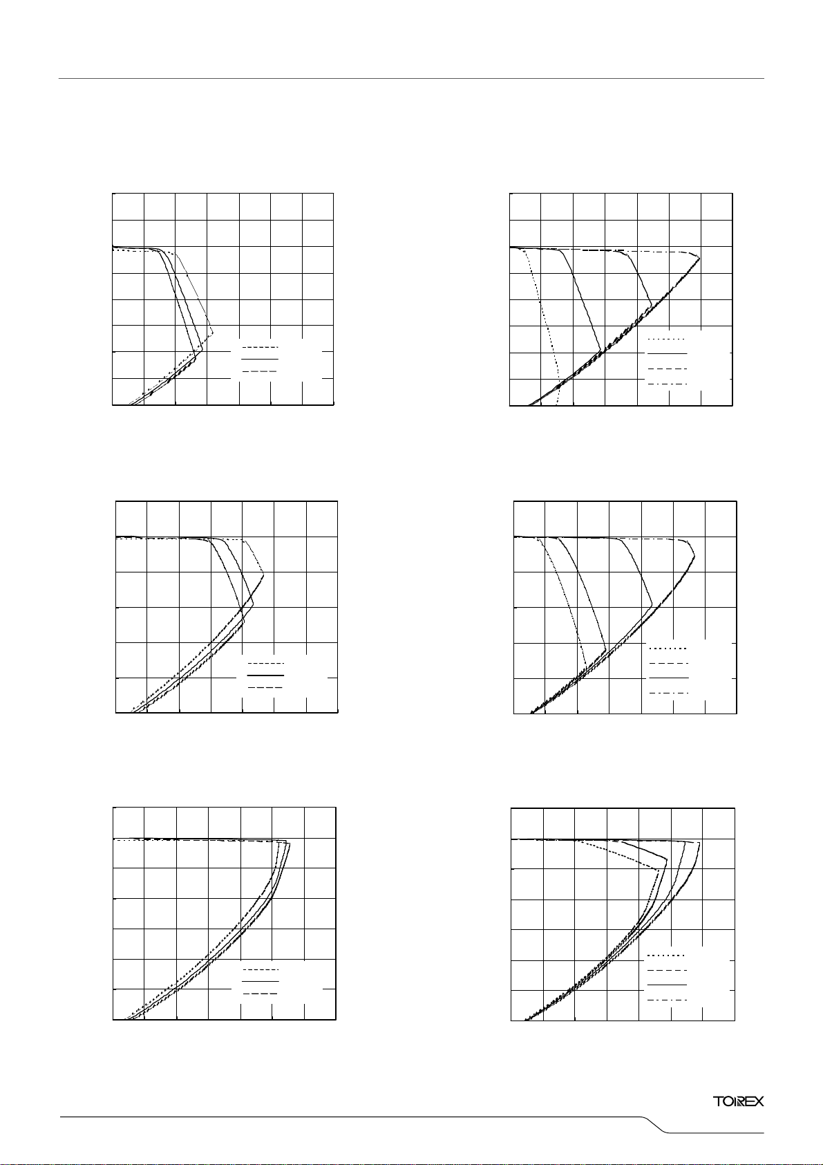
(V)
1
IN
0
-1
Input Voltage VIN (V)
-2
Output V oltage
2
Output V oltage V
1
-1
Input Voltage V
-2
-3
Tim e (50μsec/div)
0
-3
tr=5μse c
VIN=VCE =0V→1.9V , IOUT =50mA , CL=0.1 μF(ceram ic)
3
2
(V)
1
IN
0
-1
Input Voltage V
-2
XC6215x092
Output Voltage
Input Voltage
tr=5μse c
VIN=VCE =0V→2.5V , IOUT =1m A , CL= 0.1μ F(ceram ic)
6
5
(V)
4
OUT
3
2
Output V oltage V
1
3
2
(V)
1
IN
0
-1
Input Voltage V
-2
-3
Tim e (50μsec/div)
0
-3
XC6215x092
Input Voltage
Output V oltage
Tim e (50μsec/div)
XC6215x152
Input Voltage
Output Voltage
Tim e (50μsec/div)
XC6215
Series
5.5
5.0
4.5
4.0
3.5
3.0
6
5
(V)
4
OUT
3
2
Output V oltage V
1
0
6
5
(V)
4
OUT
3
2
Output V oltage V
1
0
23/36
(V)
OUT
Output Voltage V

XC6215 Series
■TYPICAL PERFORMANCE CHARACTERISTICS (Continued)
(10) Rising Response Time (Continued)
(V)
IN
Input Voltage V
6
4
(V)
2
IN
0
-2
Input Voltage V
-4
-6
6
4
(V)
2
IN
0
-2
Input Voltage V
-4
-6
24/36
tr=5μ se c
VIN=VCE =0V→2.5V, IOUT=30mA , CL=0.1μF(cerami c)
3
2
1
0
-1
-2
-3
tr=5μ se c
VIN=VCE =0V→4.0V , IOUT =1m A , CL= 0.1μ F(ceram ic)
tr=5μ se c
VIN=VCE =0V→4.0V , IOUT =10 0m A , CL =0.1 μF(ceram ic)
XC6215x152
Input Voltage
Output Voltage
Tim e (5 0μsec/div)
XC6215x302
Input Voltage
Output Voltage
Tim e (10 0μsec/div)
XC6215x302
Input Voltage
Output Voltage
Time (100μsec/div)
6
5
4
3
2
1
0
9
7.5
6
4.5
3
1.5
0
9
7.5
6
4.5
3
1.5
0
(V)
OUT
Output V oltage V
(V)
OUT
Output V oltage V
(V)
OUT
Output V oltage V
tr=5μ se c
VIN=VCE =0V→2.5V, IOUT=100mA , CL=0.1μF(cerami c)
3
2
XC6215x152
(V)
1
IN
Input Voltage
0
-1
Output Voltage
Input Voltage V
-2
-3
Tim e (50 μsec/div)
tr=5μ se c
VIN=VCE =0V→4.0V , IOUT =30 m A , CL= 0.1μ F(cera mi c)
6
XC6215x302
4
Input Voltage
(V)
2
IN
0
Output Voltage
-2
Input Voltage V
-4
-6
Time (100μsec/div)
XC6215x502
tr=5μ se c
VIN=VCE =0V→6.0V, IOUT=1m A , CL=0.1μ F(ceram ic)
9
6
Input Voltage
(V)
3
IN
0
Output Voltage
-3
Input Voltage V
-6
-9
Time (200μsec/div)
6
5
4
3
2
1
0
9
7.5
6
4.5
3
1.5
0
15
12.5
10
7.5
5
2.5
0
(V)
OUT
Output V oltage V
(V)
OUT
Output V oltage V
(V)
OUT
Output V oltage V

■TYPICAL PERFORMANCE CHARACTERISTICS (Continued)
(10) Rising Response Time (Continued)
9
tr=5μse c
VIN=VCE =0V→6.0V, IOUT=30mA , CL=0.1μF(ceram ic)
XC6215x502
15
tr=5μse c
VIN=VCE =0V→6.0V, IOUT=100mA , CL=0.1μF(ceram ic)
9
XC6215x502
6
(V)
3
IN
0
-3
Input Voltage V
-6
-9
Tim e (2 00μsec/div)
Input Voltage
Output Voltage
12.5
10
7.5
5
2.5
0
(V)
OUT
Output V oltage V
6
(V)
3
IN
0
-3
Input Voltage V
-6
-9
Tim e (2 00μsec/div)
Input Volt age
Output Voltage
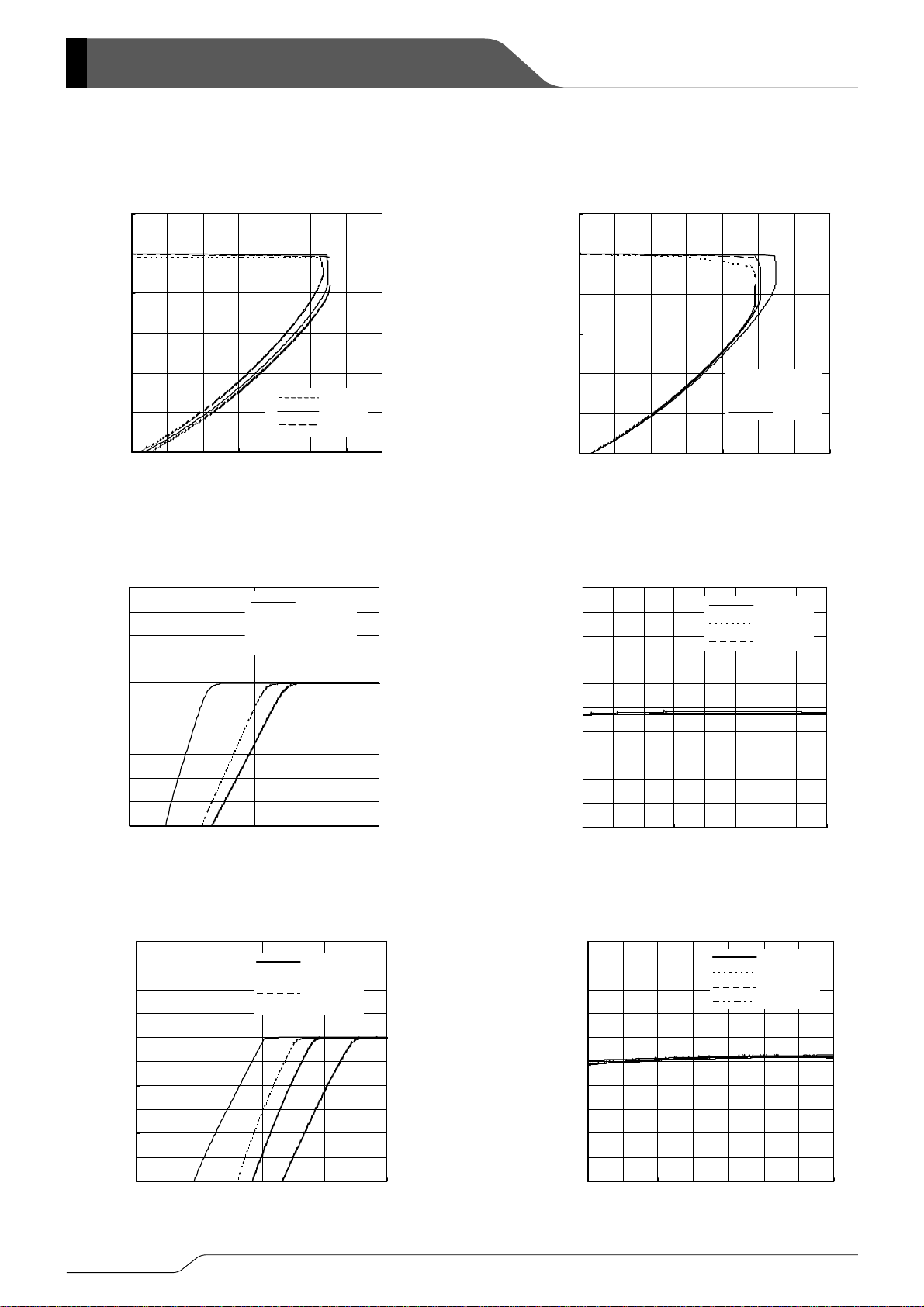
(11) CE Rising Response Time (For XC6215B Type)
3
VCE =0→1.9V , IOUT=1mA , CL=0.1 μF(ceram ic)
2
(V )
CE
1
0
-1
CE Input Voltage V
-2
-3
3
2
(V)
CE
1
0
tr=5μsec ,VIN=1.9V
VCE =0→1.9V, IOUT=5 0m A , CL=0.1μF(cerami c)
-1
CE Input Voltage V
-2
-3
XC6215B092
tr=5μsec ,VIN=1 .9V
CE Input Voltage
Output Voltage
Tim e (5 0μsec/div)
XC6215B092
CE Input Voltage
Output Voltage
Tim e (5 0μsec/div)
XC6215B092
tr=5μsec ,VIN=1.9V
6
5
(V)
4
OUT
3
2
Output Voltage V
1
0
VCE =0→1.9V, IOUT=3 0m A , CL=0.1μ F(ceram ic)
3
2
(V )
CE
1
CE Input Voltage
0
-1
CE Input Voltage V
-2
Output V oltage
-3
Tim e (5 0μsec/div)
XC6215B152
tr=5μsec ,VIN=2.5V
6
5
(V)
4
OUT
3
2
Output Voltage V
1
0
VCE =0→2.5V, IOUT=1 mA , CL=0.1μF(cerami c)
3
2
CE Input Voltage
(V )
CE
1
0
Output Voltage
CE Input V oltage V
-1
-2
-3
Time (100μsec/div)
XC6215
Series
15
12.5
10
7.5
5
2.5
0
6
5
4
3
2
1
0
6
5
4
3
2
1
0
25/36
(V)
OUT
Output V oltage V
(V)
OUT
Output V oltage V
(V)
OUT
Output Voltage V

XC6215 Series
■TYPICAL PERFORMANCE CHARACTERISTICS (Continued)
(11) CE Rising Response Time (Continued)
(V )
CE
-1
CE Input Voltage V
-2
-3
(V)
CE
CE Input Voltage V
(V )
CE
CE Input Voltage V
26/36
tr=5μsec ,VIN=2 .5V
VCE =0→2.5V , IOUT =30 mA , CL=0 .1μ F(ceramic)
3
2
1
0
tr=5μsec ,VIN=4.0V
VCE =0→4.0V , IOUT= 1m A, CL=0 .1μ F(ceram ic)
6
4
2
0
-2
-4
-6
tr=5μsec ,VIN=4.0V
VCE =0→4.0V, IOUT=100mA , CL=0.1μF(ceramic)
6
4
2
0
-2
-4
-6
XC6215B152
CE Input Voltage
Output Voltage
Time (100μsec/div)
XC6215B302
CE Input Voltage
Tim e (2 00μsec/div)
XC6215B302
CE Input Voltage
Tim e (200μsec/div)
Output Voltage
Output Voltage
XC6215B152
tr=5μsec ,VIN=2.5V
VCE =0→2.5V, IOUT=10 0m A, CL=0.1 μF(ceram i c)
(V )
CE
CE Input Voltage V
3
2
CE Input Voltage
1
0
-1
Output Voltage
-2
-3
6
5
(V )
OUT
4
3
2
Output V oltage V
1
0
Time (100μsec/div)
XC6215B302
tr=5μsec ,VIN=4.0V
VCE =0→4.0V , IOUT= 30m A , CL=0.1μ F(ceram ic)
(V )
CE
CE Input Voltage V
6
4
CE Input Voltage
2
0
Output Voltage
-2
-4
-6
6
5
4
3
2
1
0
(V)
OUT
Output V oltage V
Tim e (2 00μsec/div)
XC6215B502
tr=5μsec ,VIN=6.0V
VCE =0→6.0V , IOUT=1m A, CL=0 .1μ F(ceram ic)
6
5
(V )
4
OUT
3
2
Output V oltage V
1
0
8
6
(V )
CE
4
2
0
CE Input Voltage V
-2
-4
CE Input Voltage
Output Volt age
Tim e (2 00μsec/div)
6
5
4
3
2
1
0
6
5
4
3
2
1
0
12
10
8
6
4
2
0
(V )
OUT
Output V oltage V
(V)
OUT
Output V oltage V
(V )
OUT
Output V oltage V

■TYPICAL PERFORMANCE CHARACTERISTICS (Continued)
(11) CE Rising Response Time (For XC6215 Type)
tr=5μ sec ,VIN=6.0V
VCE = 0→6.0V, IOUT=30mA, CL=0.1μF(ceramic)
8
XC6215B502
12
tr=5μ sec ,VIN=6.0V
VCE =0→6.0V , IOUT =10 0m A , CL =0.1μF(ceram i c)
8
6
(V )
CE
4
CE Input Voltage
10
8
(V )
OUT
6
4
2
6
2
0
CE Input Voltage V
-2
Output V oltage
4
Output V oltage V
2
0
CE Input Voltage V CE (V )
-2
-4
Tim e (20 0μsec/div)
0
-4
XC6215B502
CE Input Voltage
Output V oltage
Tim e (200 μsec/div)
(12) Ripple Rejection Rate
70
60
50
40
30
20
10
Ripple Rejection Rate RR (dB)
0
0.01 0.1 1 10 100
70
60
50
40
30
20
Ripple Rejection Rate RR (dB)
10
0
0.01 0.1 1 10 100
XC6215x092
VIN=VCE=2.0VDC+0.5Vp-pAC
IOUT=50m A , CL=0.1μ F(ceram ic)
Ripple Frequency f (kHz)
XC6215x302
VIN=VCE=4.0VDC+0.5Vp-pAC
IOUT =50mA , CL=0 .1μF(ce rami c)
Ripple Frequency f (kHz)
XC6215x152
VIN=VCE=2.5VDC+0.5Vp-pAC
70
60
50
40
30
20
Ripple Rejection Rate RR (dB)
10
0
0.01 0.1 1 10 100
70
60
50
40
30
20
Ripple Rejection Rate RR (dB)
10
0
0.01 0.1 1 10 100
IOUT =50mA , CL=0.1 μF(ceram ic)
Ripple Frequency f (kHz)
XC6215x502
VIN=VCE=5.5VDC+0.5Vp-pAC
IOUT =50mA , CL=0 .1μF(cerami c)
Ripple Frequency f (kHz)
XC6215
Series
12
10
(V )
8
OUT
6
4
Output V oltage V
2
0
27/36

XC6215 Series
■PACKAGING INFORMATION
●USP-4
●USP-3
(Unit : mm)
(Unit : mm)
Reference pattern Layout Reference metal mask design
Reference pattern Layout Reference metal mask design
28/36

(
)
■PACKAGING INFORMATION
Continued
●SOT-25 ●SSOT-24
2.9±0.2
+0.1
0.4
-0.05
5 4
0〜0.1
+0.2
-0.1
1.6
2.8±0.2
0.2MIN
1
2
3
(0.95)
1.9±0.2
0.15
+0.1
-0.05
XC6215
Series
●USPN-4
1.3MAX
1.1±0.1
(Unit : mm)
(Unit : mm)
Reference pattern Layout
Reference metal mask design
(Unit: mm)
29/36

r
r
T
r
r
XC6215 Series
■MARKING RULE
●SSO
●USP-4, USP-3
(TOP VIEW)
(TOP VIEW)
-24
34
① ② ④
12
SSOT-24
(TOP VIEW)
USP-4
USP-3
① represents type of regulator and output voltage range
MARK TYPE OUTPUT VOLTAGE RANGE PRODUCT SERIES
② represents decimal point of output voltage
③
0 to 9, A to Z repeated. (G, I, J, O, Q, W excluded)
NOTE: No character inversion used.
① represents product series
MARK PRODUCT SERIES
② represents type of regulator and output voltage range
MARK TYPE OUTPUT VOLTAGE RANGE PRODUCT SERIES
③ represents output voltage
④
epresents production lot numbe
0 to 9, A to Z repeated. (G, I, J, O, Q, W excluded)
NOTE: No character inversion used.
T 0.9V ~ 3.0V
U
CE pin, High Active with no
pull-down resistor built in
3.1V ~ 5.0V
XC6215Bxxxxx
MARK OUTPUT VOLTAGE (V) MARK OUTPUT VOLTAGE (V)
0 - 3.1 - F 1.6 4.6 1 - 3.2 - H 1.7 4.7 2 - 3.3 - K 1.8 4.8 3 - 3.4 - L 1.9 4.9 4 - 3.5 - M 2.0 5.0 5 - 3.6 - N 2.1 - 6 - 3.7 - P 2.2 - 7 - 3.8 - R 2.3 - 8 0.9 3.9 - S 2.4 - 9 1.0 4.0 - T 2.5 - A 1.1 4.1 - U 2.6 - -
B 1.2 4.2 - V 2.7 - C 1.3 4.3 - X 2.8 - D 1.4 4.4 - Y 2.9 - E 1.5 4.5 - Z 3.0 - -
epresents production lot numbe
E XC6215xxxxxx
T 0.9V ~ 3.0V
U
CE pin, High Active with no
pull-down resistor built in
3.1V ~ 5.0V
XC6215xxxxxx
MARK OUTPUT VOLTAGE (V) MARK OUTPUT VOLTAGE (V)
0 - 3.1 - F 1.6 4.6 -
1 - 3.2 - H 1.7 4.7 -
2 - 3.3 - K 1.8 4.8 -
3 - 3.4 - L 1.9 4.9 -
4 - 3.5 - M 2.0 5.0 -
5 - 3.6 - N 2.1 - -
6 - 3.7 - P 2.2 - -
7 - 3.8 - R 2.3 - -
8 0.9 3.9 - S 2.4 - -
9 1.0 4.0 - T 2.5 - A 1.1 4.1 - U 2.6 - B 1.2 4.2 - V 2.7 - C 1.3 4.3 - X 2.8 - D 1.4 4.4 - Y 2.9 - E 1.5 4.5 - Z 3.0 - -
30/36

(
)
T
r
r
■MARKING RULE
●SO
-25
54
① ② ③ ④ ⑤
123
SOT-25
(TOP VIEW)
●USPN-4
USPN-4
(TOP VIEW)
XC6215
Series
Continued
① represents product series
MARK PRODUCT SERIES
E XC6215xxxxxx
② represents type of regulators and output voltage range
MARK TYPE OUTPUT VOLTAGE RANGE PRODUCT SERIES
T 0.9V~3.0V
U
③ represents output voltage
MARK OUTPUT VOLTAGE (V) MARK OUTPUT VOLTAGE (V)
0 - 3.1 - F 1.6 4.6 1 - 3.2 - H 1.7 4.7 2 - 3.3 - K 1.8 4.8 3 - 3.4 - L 1.9 4.9 4 - 3.5 - M 2.0 5.0 5 - 3.6 - N 2.1 - 6 - 3.7 - P 2.2 - 7 - 3.8 - R 2.3 - 8 0.9 3.9 - S 2.4 - 9 1.0 4.0 - T 2.5 - -
A 1.1 4.1 - U 2.6 - B 1.2 4.2 - V 2.7 - C 1.3 4.3 - X 2.8 - D 1.4 4.4 - Y 2.9 - E 1.5 4.5 - Z 3.0 - -
④⑤
0 to 9, A to Z repeated. (G, I, J, O, Q, W excluded)
NOTE: No character inversion used.
CE pin, High Active with no
pull-down resistor built in
epresents production lot numbe
3.1V~5.0V
XC6215xxxxxx
31/36

p
(
)
XC6215 Series
● SOT-25 Power Dissipation
Power dissipation data for the SOT-25 is shown in this page.
The value of power dissipation varies with the mount board conditions.
Please use this data as one of reference data taken in the described
condition.
1. Measurement Condition (Reference data)
Condition: Mount on a board
Ambient: Natural convection
Soldering: Lead (Pb) free
Board: Dimensions 40 x 40 mm (1600 mm
Copper (Cu) traces occupy 50% of the board area
Material: Glass Epoxy (FR-4)
Thickness: 1.6 mm
Through-hole: 4 x 0.8 Diameter
2. Power Dissipation vs. Ambient temperature
Board Mount (Tj max = 125℃)
Ambient Temperature(℃) Power Dissipation Pd(mW) Thermal Resistance (℃/W)
In top and back faces
Package heat-sink is tied to the copper traces
(Board of SOT-26 is used.)
2
in one side)
評価基板レイアウト(単位:mm)
Evaluation Board (Unit: mm)
25 600
85 240
Pd-Ta特性グラフ
Pd vs. Ta
700
mW
600
166.67
500
400
ation Pd
300
200
100
許容損失Pd(mW)
Power Dissi
0
25 45 65 85 105 125
Ambient Temperature Ta (℃)
周辺温度Ta(℃)
32/36

● SSOT-24 Power Dissipation
Power dissipation data for the SSOT-24 is shown in this page.
The value of power dissipation varies with the mount board conditions.
Please use this data as one of reference data taken in the described
condition.
1. Measurement Condition (Reference data)
Condition: Mount on a board
Ambient: Natural convection
Soldering: Lead (Pb) free
Board: Dimensions 40 x 40 mm (1600 mm
Copper (Cu) traces occupy 50% of the board area
In top and back faces
Package heat-sink is tied to the copper traces
Material: Glass Epoxy (FR-4)
Thickness: 1.6 mm
Through-hole: 4 x 0.8 Diameter
2
in one side)
2. Power Dissipation vs. Ambient temperature
Board Mount (Tj max = 125℃)
Ambient Temperature(℃) Power Dissipation Pd(mW) Thermal Resistance (℃/W)
25 500
85 200
200.00
XC6215
Series
Evaluation Board (Unit: mm)
33/36

XC6215 Series
● USP-4 Power Dissipation
Power dissipation data for the USP-4 is shown in this page.
The value of power dissipation varies with the mount board conditions.
Please use this data as one of reference data taken in the described
condition.
1. Measurement Condition (Reference data)
Condition: Mount on a board
Ambient: Natural convection
Soldering: Lead (Pb) free
Board: Dimensions 40 x 40 mm (1600 mm
Copper (Cu) traces occupy 50% of the board area
In top and back faces
Package heat-sink is tied to the copper traces
Material: Glass Epoxy (FR-4)
Thickness: 1.6 mm
Through-hole: 4 x 0.8 Diameter
2. Power Dissipation vs. Ambient temperature
Board Mount (Tj max = 125℃)
Ambient Temperature(℃) Power Dissipation Pd(mW) Thermal Resistance (℃/W)
2
in one side)
40.0
28.9
28.9
2.54
Evaluation Board (Unit: mm)
1.4
40.0
2.5
25 1000
85 400
100.00
34/36

● USPN-4 Power Dissipation
Power dissipation data for the USPN-4 is shown in this page.
The value of power dissipation varies with the mount board conditions.
Please use this data as one of reference data taken in the described
condition.
1.Measurement Condition (Reference data)
Condition: Mount on a board
Ambient: Natural convection
Soldering: Lead (Pb) free
Board: Dimensions 40 x 40 mm (1600 mm
Material: Glass Epoxy (FR-4)
Thickness: 1.6 mm
Through-hole: 4 x 0.8 Diameter
Copper (Cu) traces occupy 50% of the front and 50%
of the back.
The copper area is divided into four block,
one block is 12.5% of total.
The USPN-4 package has for terminals.
Each terminal connects one copper block in the front and
one in the back.
2
in one side)
2. Power Dissipation vs. Ambient temperature
Board Mount (Tj max = 125℃)
Ambient Temperature(℃) Power Dissipation Pd(mW) Thermal Resistance (℃/W)
XC6215
Series
Evaluation Board (Unit: mm)
25 600
85 240
166.67
35/36

XC6215 Series
1. The products and product specifications contained herein are subject to change without
notice to improve performance characteristics. Consult us, or our representatives
before use, to confirm that the information in this datasheet is up to date.
2. We assume no responsibility for any infringement of patents, patent rights, or other
rights arising from the use of any information and circuitry in this datasheet.
3. Please ensure suitable shipping controls (including fail-safe designs and aging
protection) are in force for equipment employing products listed in this datasheet.
4. The products in this datasheet are not developed, designed, or approved for use with
such equipment whose failure of malfunction can be reasonably expected to directly
endanger the life of, or cause significant injury to, the user.
(e.g. Atomic energy; aerospace; transport; combustion and associated safety
equipment thereof.)
5. Please use the products listed in this datasheet within the specified ranges.
Should you wish to use the products under conditions exceeding the specifications,
please consult us or our representatives.
6. We assume no responsibility for damage or loss due to abnormal use.
7. All rights reserved. No part of this datasheet may be copied or reproduced without the
prior permission of TOREX SEMICONDUCTOR LTD.
36/36

 Loading...