

TOPSTAR S42C Schematics
5
hexainf@hotmail.com
GRATIS - FOR FREE
4
3
2
1
Topstar Digital technologies Co.,LTD
D D
Board name: Mother Board Schematic
Project name: S42G
Version: VerD
Release Date: Jan.08, 2008
1. System Block Diagram & Schematic page description;
2. Power Block Diagram & Discription;
3. Annotations & information;
4. Schematic modify Item and history;
5. Power on & off Sequence;
C C
6. ACPI Mode Switch Timings;
7. Power On Sequence Map;
8. CLOCK Distribution;
9. Power Distribution;
Topstar Confidential
B B
Hardware drawing by:
Power drawing by:
Hardware check by: EMI Check by:
Power check by:
Manager Sign by:
TOPSTAR TECHNOLOGY
TOPSTAR TECHNOLOGY
A A
5
4
3
2
Page Name
Page Name
Page Name
Size
Size
Size
Project Name Rev
Project Name Rev
Project Name Rev
B
B
B
Date: Sheet
Date: Sheet
Date: Sheet
PROPERTY NOTE: this document contains information confidential and property to
PROPERTY NOTE: this document contains information confidential and property to
PROPERTY NOTE: this document contains information confidential and property to
TOPSTAR and shall not be reproduced or transferred to other documents or disclosed
TOPSTAR and shall not be reproduced or transferred to other documents or disclosed
TOPSTAR and shall not be reproduced or transferred to other documents or disclosed
to others or used for any purpose other than that for which it was obtained without
to others or used for any purpose other than that for which it was obtained without
to others or used for any purpose other than that for which it was obtained without
the expressed written consent of TOPSTAR
the expressed written consent of TOPSTAR
the expressed written consent of TOPSTAR
TOPSTAR TECHNOLOGY
Echo liu
Echo liu
Echo liu
Title
Title
Title
S42C
S42C
S42C
151Saturday, September 27, 2008
151Saturday, September 27, 2008
151Saturday, September 27, 2008
1
A
A
A
of
of
of
5
4
3
2
1
Topstar Confidential
D D
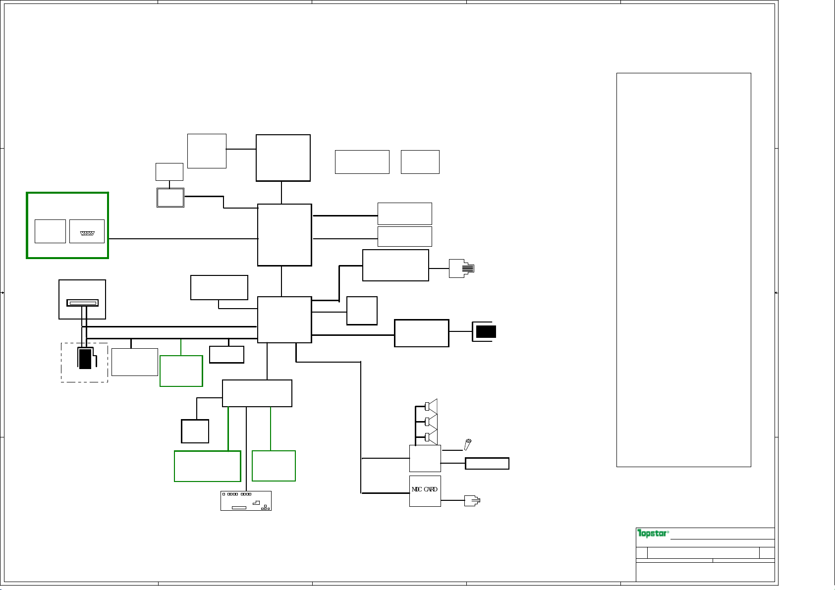
VGA BRD
C C
B B
A A
Camera
1.3M pixel
+V5AL
VGA BOARD
PCIE mini Card
WLAN
PG 33
PCIE 1X
PCIE 1X
NEW CARD(Type II)
PG 31
+V5S
BLUE
TOOTH(V1.2)
MDCBTASC32
+V5AL +V3.3AL
+V3.3S
PG 38
ShenZhen Topstar Industry Co.,LTD
S42C SYSTEM BLOCK Ver:A
Backlight
Connector
+VDC
TFT
+V3.3S
PCIE 1X
USB1.1/2.0
2 PORT
USB&LAN
DAUGHTER
BOARD
CPU
Thermal
Sensor
F75393S
+V3.3S
PG 7
S-ATAII
DVD
+V5S
PG 28
USB PORT1
+V5AL
PG 34
SPI
BIOS
8Mbit
+V3.3AL
PG 35
LED & TouchPAD
DAUGHTER
BOARD
LVDS
R/G/B
KB Controller/EC
ENE KB3310B0
KB Matrix
+V3.3S
QButton
DAUGHTER
BOARD
+VCC_CORE,+VCCP
+VCCA1.5
Merom/
Merom_Lite
478 uFCPGA
PG 7,8
FSB
1066/800/667MHz
@8.5/6.4GB/s
SIS672DX
BGA 847
+V1.8S, +1.05S,
+V1.2S,+V1.8AL,
+V1.8,+V1.2AL
PG 9,10,11,
12,13,14
MutioL
16bit*133MHZ*4Mode
@1GB/s
SIS968
570 BGA
+V1.05S,+V3.3S
+V1.8S,+V5S
+V3.3AL,+V1.8AL
+V2.5AL_LAN
ICH_EC_RTC
PG 25,26,27
LPC
PG 35
DDR2 533/667
@5.3GB/s
DDR2 533/667
MII
@300MB/s
USB2.0
@480Mb/s
AZALIA
CLK Generator:
RTM870T-670
+V3.3S
S-ATAII
2.5" HDD
+V5S,+V3.3S
PG 28
PG 6
DDR2 SODIMM0
533/667
+V0.9S,+V1.8,+V3.3S
PG 15,17,18
DDR2 SODIMM1
533/667
+V0.9S,+V1.8,+V3.3S
PG 16,17,18
LAN Phy
8201CL
+V3.3AL/+V3.3S,
PWFBOUT(1.8V/Internal)
PG 32
CardReader
RTS5158
+V3.3S,+V3.3AL
PG 29,30
CLK buffer
+V1.8
PG 6
Speaker
AZALIA
ALC883
+V5S,+V3.3S
PG 37
Azalia
MDC CAR
+V3.3S
PG 38
Bass
INDEX
01 Title
02 System Block & Index
03 PWR Block & Description
04 Notes and Annotations
05 Sch Modify and History
06 CLK_Gen_Buffer(CLK)
07 Merom CPU(Host BUS)(1of 2)
08 Merom CPU(PWR&GND)(2 of 2)
09 SiS672_HOST_PCIE(1/5)
10 SiS672_DDRII(2/5)
11 SiS672_MuTIOL_VGA(3/5)
12 SiS672_PWR(4/5)
13 SiS672_GND(5/5)
14 DDR2 SODIMM0
15 DDR2 SODIMM1
16 DDR2 Termination_decoupling
17 307LVDS
18 LVDS&Inverter CONN
19 CRT&S-VIDEO CONN & LIDR
20 968-1 PCI/IDE/MuTIOL/SPI
21 968-2 Host/LPC/PCIE/MAC/GPIO
22 968-3 USB/SATA
23 968-4 Power
24 IDE/SATA CONN(SATA&DVD)
RJ45
SD/MMC/MS CARD
L
R
MiC
Audio Jack
PG 37
D
RJ11
25 Card Reader(UB6232 USB)
26 NEW CARD
27 MII LAN PHY (RTL8201CL 100M)
28 MPCIE SLOT(WLAN)
29 USB PORTX&TP&LED&QB Con
30 KBC(PC87541L)
31 ALC662 Azalia codec
32 MDC&BT/FAN/OTP
33 ADAPTER IN
34 BATTERY IN/OVP
35 +V3.3AL +V5AL
36 +V1.8/+V0.9S DDR
37 +V1.2S
38 V5S/V3.3S/V1.8S Power
39 2.5AL/1.8AL/1.5S/1.05S LDO
40 Power Good Logic/OVP
41 DISCHARGE Circuit
42 +VCC_CORE
43 CHARGER
44 THROUGH HOLE/EMI
45 Clock Distribution
46 Power Distribution
47 Power ON/OFF Timing
48 ACPI mode switch timings
49 PowerOnSequence & Reset Map
50 ResetMap/NMI/SMI/THERMAL
51 CPU C STATE/GPIO
TOPSTAR TECHNOLOGY
TOPSTAR TECHNOLOGY
TOPSTAR TECHNOLOGY
Echo liu
Echo liu
Page Name
Page Name
Page Name
Size
Size
Size
Project Name Rev
Project Name Rev
Project Name Rev
C
C
C
Date: Sheet
Date: Sheet
Date: Sheet
PROPERTY NOTE: this document contains information confidential and property to
PROPERTY NOTE: this document contains information confidential and property to
PROPERTY NOTE: this document contains information confidential and property to
TOPSTAR and shall not be reproduced or transferred to other documents or disclosed
TOPSTAR and shall not be reproduced or transferred to other documents or disclosed
TOPSTAR and shall not be reproduced or transferred to other documents or disclosed
to others or used for any purpose other than that for which it was obtained without
to others or used for any purpose other than that for which it was obtained without
to others or used for any purpose other than that for which it was obtained without
the expressed written consent of TOPSTAR
the expressed written consent of TOPSTAR
5
4
3
2
the expressed written consent of TOPSTAR
Echo liu
System Block & Index
System Block & Index
System Block & Index
S42C
S42C
S42C
1
A
A
251Sunday, September 28, 2008
251Sunday, September 28, 2008
251Sunday, September 28, 2008
A
of
of
of
5
hexainf@hotmail.com
GRATIS - FOR FREE
4
3
2
1
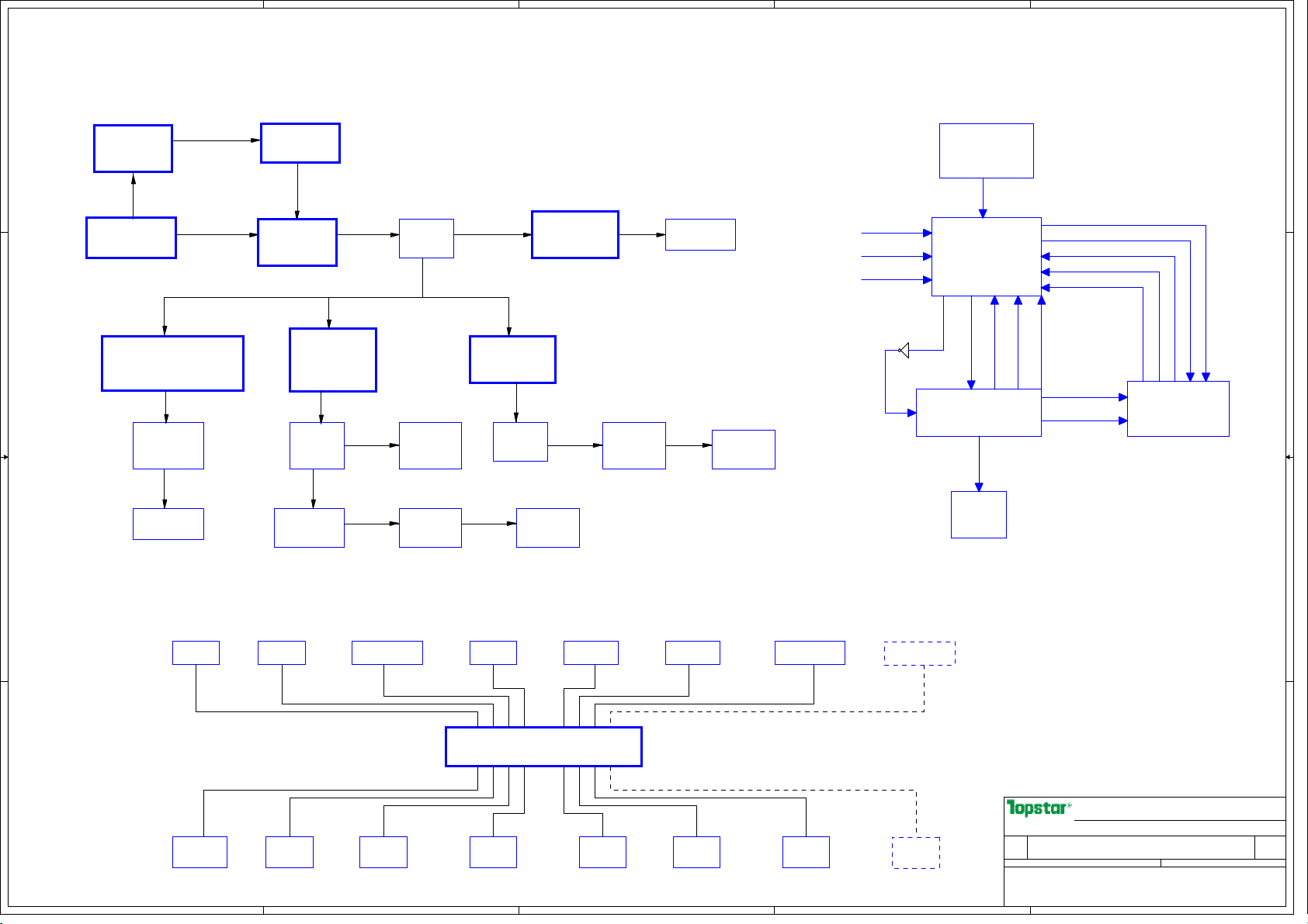
S42C POWER BLOCK Ver:A
D D
Charger
ISL6251
PU9
Battery
Platform
Logic
VR_ON
Adapter
18.5-19.5V
Power
Switch
+VDC
VCC_CORE
ISL6262A
PU5
44A
+VCC_CORE
VIN
V_5
IMVP-6
V_3
C C
VGA/+V1.2S PWR
TPS51124
PU3
+V1.2S
+VGA_CORE
LDO
+V1.05S
B B
Always_On
Power
TPS51120
PU1
+V3.3AL
+V5AL
LDO
+V_LAN
(+V2.5AL)
MOSFET
Switch
LDO
+V5S
+V3.3S
+V1.8AL
DDR Power
TPS51116
PU2
+V1.8
+V0.9S
LDO
+V1.2AL
MOSFET
Switch
+V1.8S
LDO
+V1.5S
CLK_ENABLE#
IMVP6_PWRGD
SIS968
CLK
CHIP
DPRSLPVR
Vcc_sense
VR_TT#
Vcc_core
VID[6...0]
PSI#
DPRSTP#
Vss_sense
DPRSTP#
CPU_PWRGD
PSI#
CPU-M
PROCHOT#
BATT+
+V5AL +V1.05S
+V3.3AL
+V1.8
+V1.5S
+VCC_CORE
+VGA_CORE
OVP Circuit
Page 43,52
A A
Page Name
Page Name
Page Name
Size
Size
Size
Project Name Rev
Project Name Rev
Project Name Rev
A3
A3
A3
Date: Sheet
Date: Sheet
Date: Sheet
PROPERTY NOTE: this document contains information confidential and property to
PROPERTY NOTE: this document contains information confidential and property to
PROPERTY NOTE: this document contains information confidential and property to
TOPSTAR and shall not be reproduced or transferred to other documents or disclosed
TOPSTAR and shall not be reproduced or transferred to other documents or disclosed
TOPSTAR and shall not be reproduced or transferred to other documents or disclosed
to others or used for any purpose other than that for which it was obtained without
to others or used for any purpose other than that for which it was obtained without
to others or used for any purpose other than that for which it was obtained without
the expressed written consent of TOPSTAR
the expressed written consent of TOPSTAR
the expressed written consent of TOPSTAR
OVP
16.5V
5
OVP
5.6V
OVP
3.6V
OVP
2.0V
4
OVP
2.0V
OVP
2.0V
3
OVP
2.0V
OVP
2.0V
2
TOPSTAR TECHNOLOGY
TOPSTAR TECHNOLOGY
TOPSTAR TECHNOLOGY
Echo liu
Echo liu
Echo liu
PWR Block & description
PWR Block & description
PWR Block & description
S42C
S42C
S42C
1
A
A
351Sunday, September 28, 2008
351Sunday, September 28, 2008
351Sunday, September 28, 2008
A
of
of
of
5
A
Voltage Rails
+VDC
+VCC_CORE
+V1.5S
D D
+V1.05S
+V0.9S
+V1.8
+V3.3AL
+V3.3S
+V5AL
+V5S
+V1.2S
+V1.8S
Primary DC system power supply(9V-19V)
Core voltage for processor
1.5V for CPU PLL
1.05V for FSB VTT
0.9V DDR2 Termination voltage
1.8V power rail for DDR2
3.3V always on power rail
3.3V main power rail
5V for USB Device
5V main power rail
1.2V PCIE IO,PLL,SIS671DX Core
1.8V SIS672/SIS968 Core/SATA/USB/PCIE
4
3
2
1
I2C SMB Address
Device
Clock Generator
SO-DIMM0
SO-DIMM1
NEW CARD
PCIE Mini CARD
Smart Battery
CPU Thermal
Sensor(F75383S)
Address
1101 111x
1010 000x
1001 100x
D2
A0
A2
Variable SMB_ICH_SVariable SIS968
Variable SMB_ICH_SVariable SIS968
160001 011x
98
BusHex
SMB_ICH_S
SMB_ICH_S
SMB_ICH_S1010 001x
I2C_591
I2C_591
Master
SIS968
SIS968
SIS968
Embeded Controller(EC)
Pin169/170
Embeded Controller(EC)
Pin163/164
PCI Devices
Bus # Device # Function # Device ID IDSEL INTX Device Function
SIS968:
Bus 0 Device 2 Function 0 0008h AD13 N/A LPC
Bus 0 Device 2 Function 5 5513h/1180h/1181h AD13 INTA IDE
Bus 0 Device 3 Function 0 7001h AD14 INTE USB 1.1 #0
C C
Board stack up description
PCB Layers
TOP
VCC
IN1
Trace Impedence:55ohm +/-15%(Default)
Bus 0 Device 3 Function 1 7001h AD14 INTF USB 1.1 #1
Bus 0 Device 3 Function 3 7002h AD14 INTG USB 2.0
Bus 0 Device 4 Function 0 0191h AD15 INTD LAN
Bus 0 Device 5 Function 0 1183h/1184h/1185h AD16 INTB SATA
Bus 0 Device 6 Function 0 000Ah AD17 INTA/B/C/D PCI Express 0
Bus 0 Device 7 Function 0 000Ah AD18 INTA/B/C/D PCI Express 1
Bus 0 Device F Function 0 7502h AD26 INTC HD Audio
SIS672:
Bus 0 Device 0 Function 0 0671h AD11 North Bridge
Bus 0 Device 31 Function 0 0004h AD31 Virtual PCI-to-PCI Bridge for
PCI-Express device
IN2
Onboard Devide:NON
GND
Bottom
B B
USB Table
USB Port#
0
1
2
3
4
5
6
7
Function Description
USB Port(on Main Board)
Mini PCIE Card(WLAN & ROBSON)
Express Card
USB CAMERA(On VGA Board)
Bluetooth
UB6232 CARD Reader
USB Port(on I/O Board)
USB Port(on I/O Board)
Power States/AC mode
Signal
S0(Full On)
S3(STM)
S4(STD)
S5(SoftOff)
SLP_S3#
HIGH
LOW
LOW OFF
LOW
SLP_S4#
HIGH
HIGH ON OFF
LOW
LOW
SLP_S5#
HIGH
HIGH
HIGH
LOW
+V*AL
ON
ON
ON
Wake up Events
Wake up by LAN/968GMAC Internal
LID switch from EC
Power switch from EC
ns: Component marked "ns" is not stuff
This is a lead free project,all component must be LF
+V*
+V*S
ON ON
ON
OFF
OFF
OFF
Page Name
Page Name
Page Name
Size
Size
Size
Date: Sheet
Date: Sheet
Date: Sheet
PROPERTY NOTE: this document contains information confidential and property to
PROPERTY NOTE: this document contains information confidential and property to
PROPERTY NOTE: this document contains information confidential and property to
TOPSTAR and shall not be reproduced or transferred to other documents or disclosed
TOPSTAR and shall not be reproduced or transferred to other documents or disclosed
TOPSTAR and shall not be reproduced or transferred to other documents or disclosed
to others or used for any purpose other than that for which it was obtained without
to others or used for any purpose other than that for which it was obtained without
to others or used for any purpose other than that for which it was obtained without
the expressed written consent of TOPSTAR
the expressed written consent of TOPSTAR
the expressed written consent of TOPSTAR
OFF
Project Name Rev
Project Name Rev
Project Name Rev
A3
A3
A3
Clock
ON
OFF
OFF
TOPSTAR TECHNOLOGY
TOPSTAR TECHNOLOGY
TOPSTAR TECHNOLOGY
Echo liu
Echo liu
Echo liu
NOTE
NOTE
NOTE
S42C
S42C
S42C
451Saturday, September 27, 2008
451Saturday, September 27, 2008
451Saturday, September 27, 2008
A
A
A
of
of
of
A
5
hexainf@hotmail.com
GRATIS - FOR FREE
4
3
2
1
Schematic modify Item and history:
2007-08-31 Ver A initial release
2007-02-09 Ver B Change List
1.PG6 C218,C212,C331,C341 footprint from 1206 to 0805.Add C622,C623,C119,C120,C128 for EMI reserved.
2.PG6 Clock Enable : change R156 from 10K to 51K,ns C344,install C142
3.PG6 FSB : Add R673 and R674, ns R148,R151 ,R145,install R155 and R147.
4.PG11 : Change C573 and C574 net from DACAVDD2 to DACAVDD1
D D
5.PG15 Add DIMM2 and surrounding Capacitor
6.PG21 : Add clear_cmos point.
7.PG22 : Change R421 value from 127 to 130 Ohm
8.PG26 Power Switch: Add Power Switch and surrounding circuit.
9.PG29 USB: Delete CHK3, and R331 and R329
10.PG30: PCB version from A to B
2007-03-09 Ver C Change List
1.PG19: Change VGA Connector
2.PG30: PCB version from B to C
2007-04-29 Ver D Change List
1. PG32 & PG21:Add modem and surrounding circuit
2. PG30: PCB version from C to D,Reserved R691
3. PG44:Change H3,H7 and H9 footprint from TH_315_112 to TH_315_118
4. PG33:Co-lay PD5 and PD8
C C
5. PG36:Co-lay PC164
2007-05-28 Ver E Change List
1.
改了板边,升级
2008-09-11 Ver F Change List
1.
改了板边,升级
2008-09-22 S42C Ver A Change List,
1. Delete CLKGEN_PWRGD circuit, NS R124,pull high PECLK2/3/5_REQ# and STOP_PCI_L#.
2. pull high CPU_STOP# because of no C3 and C4 function to realtek clock,change 56 ohm parallel resistor to 0 ohm paraller resistor.
3. R24,R26 footprint from 0603 to 0402
4. Delete paraller DVD net,and pull down or up according to SIS FAE suggest.
5. Reserved SPI BIOS ROM for SIS968, add R170
6. Delete LDRQ# off connector and R148,Delete reserved power on/S3/S4 control circuit.
7. Delete parallel DVD net add pull down or up according to SIS FAE suggest
8. Add reserved SPI ROM
9. Add SATA ODD,NS Q40 and R481,NS PQ58 and R489
10.
11. Delete Co-layout card reader connector.
B B
12. Delete Co-layout Newcard powerswitch circuit
13.Change minipcie according to minipcie 1.2 spec
14. change EC form 87541 to KB3310B
15. Delete CD_IN circuit.
16.
17.
18.
PCB
的料号从
PCB
的料号从
添加
SATA DVD的Connector
删掉
BAT_TEM circuit
根据采购以及CE的意见,更改
根据采购意见,更换
CPU Vcore的Mosfet
VerD到VerE.
VerD到VerE.
主要换了
realtek clock和新EC(KB3310B
)
F75383 to F75393, U16 from ATMEL to SEIKO,U15 from RICHON to ENE,PU5 from KIA to APEC.
。
A A
TOPSTAR TECHNOLOGY
TOPSTAR TECHNOLOGY
TOPSTAR TECHNOLOGY
Echo liu
Echo liu
Page Name
Page Name
Page Name
Size
Size
Size
Project Name Rev
Project Name Rev
Project Name Rev
Custom
Custom
Custom
Date: Sheet
Date: Sheet
Date: Sheet
PROPERTY NOTE: this document contains information confidential and property to
PROPERTY NOTE: this document contains information confidential and property to
PROPERTY NOTE: this document contains information confidential and property to
TOPSTAR and shall not be reproduced or transferred to other documents or disclosed
TOPSTAR and shall not be reproduced or transferred to other documents or disclosed
TOPSTAR and shall not be reproduced or transferred to other documents or disclosed
to others or used for any purpose other than that for which it was obtained without
to others or used for any purpose other than that for which it was obtained without
to others or used for any purpose other than that for which it was obtained without
the expressed written consent of TOPSTAR
the expressed written consent of TOPSTAR
5
4
3
2
the expressed written consent of TOPSTAR
Echo liu
Sch Modify and history
Sch Modify and history
Sch Modify and history
S42C
S42C
S42C
1
A
A
551Saturday, September 27, 2008
551Saturday, September 27, 2008
551Saturday, September 27, 2008
A
of
of
of
5
+V3.3S
FB37
FB37
100ohm@100MHz,3A
100ohm@100MHz,3A
FB0805
FB0805
1 2
D D
C0805
C0805
C331
C331
C332
C332
10uF/6.3V,X5R
10uF/6.3V,X5R
0.1uF/25V,Y5V
0.1uF/25V,Y5V
0.1uF/25V,Y5V
0.1uF/25V,Y5V
C334
C334
C328
C328
0.1uF/25V,Y5V
0.1uF/25V,Y5V
0.1uF/25V,Y5V
0.1uF/25V,Y5V
C333
C333
C342
C342
0.1uF/25V,Y5V
0.1uF/25V,Y5V
0.1uF/25V,Y5V
0.1uF/25V,Y5V
C343
C343
C329
C329
CLKGEN_VDD
0.1uF/25V,Y5V
0.1uF/25V,Y5V
0.1uF/25V,Y5V
0.1uF/25V,Y5V
C330
C330
SB_PWRGD21,30,40
CPUSTP#22
+V3.3S
S42C/Delete CLKGEN_PWRGD circuit.LJ080912
C341
C C
+V3.3S
R156
R156
51K
R369
R369
10K
10K
ns
ns
SIS_CLK_EN#42
B B
+V1.8
R367 1KR367 1K
1
C344
C344
ns
ns
0.1UF/25V,Y5V
0.1UF/25V,Y5V
51K
3
Q32
Q32
2N7002
2N7002
SOT23
SOT23
C142
2
C142
0.1UF/25V,Y5V
0.1UF/25V,Y5V
C341
SMB_DATA_S14,15,21,26,28
SMB_CLK_S14,15,21,26,28
+V3.3AL
VCC
VCC
1
2
GND
GND
ns C344,change R156 value from 10K to 51K.080401LJ
FB26
FB26
100ohm@100MHz,3A
100ohm@100MHz,3A
FB0805
FB0805
1 2
C0805
C0805
C218
C218
10uF/6.3V,X5R
10uF/6.3V,X5R
+V1.8
A A
C0805
C0805
C212
C212
C212 footprint from 1206 to 0805.lj080201
C222
C222
C215
C215
C218 footprint from 1206 to 0805.lj080201
FB25
FB25
10uF/6.3V,X5R
10uF/6.3V,X5R
0.1UF/25V,Y5V
0.1UF/25V,Y5V
0.1UF/25V,Y5V
0.1UF/25V,Y5V
120ohm@100MHz,500mA
120ohm@100MHz,500mA
12
FB0603
FB0603
C214
C214
5
C217
C217
C216
C216
0.1UF/25V,Y5V
0.1UF/25V,Y5V
CLKBUF_AVDD
0.1UF/25V,Y5V
0.1UF/25V,Y5V
CLKBUF_VDD
C223
C223
0.1UF/25V,Y5V
0.1UF/25V,Y5V
C213
C213
0.1UF/25V,Y5V
0.1UF/25V,Y5V
0.1UF/25V,Y5V
0.1UF/25V,Y5V
SMB_DATA_S14,15,21,26,28
SMB_CLK_S14,15,21,26,28
DDR_FBIO
4
1. ICS9LPR600_TSSOP-56P
2. RTM870T-670
3. SLG8LP701B
U2
CLKGEN_VDD
SIS_CLK_EN
R107 0 nsR107 0 ns
R110 0
R110 0
FB38 120ohm@100MHz,500mA
FB38 120ohm@100MHz,500mA
C0805
C0805
10uF/6.3V,X5R
10uF/6.3V,X5R
R159 0R159 0
53
DDR_FWD_CLK#10
DDR_FWD_CLK10
R457 0R457 0
R456 22R456 22
C463
C463
10pF/50V,NPO
10pF/50V,NPO
CPUSTOPIN#_SYSRSTOUT#
Realtek:ns/ICS: install
Realtek:ns/ICS: install
CLK_VDDA
12
C335
C335
FB0603
FB0603
0.1UF/25V,Y5V
0.1UF/25V,Y5V
R130 0R130 0
R133 0R133 0
C143
C143
0.1UF/10V,X7R
0.1UF/10V,X7R
4
SOT23_5
SOT23_5
SN74AHC1G08DBV
SN74AHC1G08DBV
U3
U3
ns
ns
Please base on your design to choose the appropriate capacitor vaule.
C210+C_X1+C_trace1=C1
C211+C_X2+C_trace2=C2
C_load(refer to the crystal datasheet)=(C1*C2)/(C1+C2)
CLKBUF_VDD
R459 0 nsR459 0 ns
R458 0 nsR458 0 ns
4
C338
C338
0.01uF/16V,X7R
0.01uF/16V,X7R
Layout note:
SIS_CLK_EN
1. ICS9P935_SSOP-28P
2. RTM683-910
3. SLG74201
11
25
21
10
20
DDR_FBIN
DDR_FBOUT
19
18
28
24
14
U2
2
VDDREF
14
VDDPCI_1
19
VDDPCI_2
23
VDDZ
24
VDD48
56
VDDCPU
39
VDDPCIEX_1
29
VDDPCIEX_2
7
GNDREF
8
GNDPCI_1
13
GNDPCI_2
20
GNDZ
27
GND48
53
GNDCPU
42
GNDPCIEX_1
32
GNDPCIEX_2
1
VTTPWRGD/PD#/(CLK_STOP#)
28
*(CPU_STOP#)/RESET#
50
VDDA
47
GNDA
45
SDATA
46
SCLK
X1
5
Y2 14.31818M 3.0mm
Y2 14.31818M 3.0mm
1 2
C133
C133
33pF/50V,NPO
33pF/50V,NPO
MP:Change footprint from 0603 to 0402.LJ0308
change to 3.0mm Height Crystal
U17
3
VDD1.8_1
VDD1.8_2
VDD1.8_3
VDD1.8_4
CLK_INC
9
CLK_INT
SDATA
SCLK
FB_IN
FB_OUT17DDRT3
8
GND_1
6
GND_2
GND_3
GND_4
GND_5
RTM683-910
RTM683-910
SOP28_0D65_5D3
SOP28_0D65_5D3
U17
VDDA1.8
DDRC0
DDRT0
DDRC1
DDRT1
DDRC2
DDRT2
DDRC3
DDRC4
DDRT4
DDRC5
DDRT5
7
1
2
5
4
13
12
15
16
23
22
27
26
CLKBUF_AVDD
3
CPUT_L0
CPUC_L0
CPUT_L1
CPUC_L1
PCIET_L0
PCIEC_L0
PCIET_L1
PCIEC_L1
PCIET_L2
PCIEC_L2
PCIET_L3
PCIEC_L3
PCIET_L4F
PCIEC_L4F
PCIET_L5F
PCIEC_L5F
SATACLKT_L
SATACLKC_L
ZCLK0
ZCLK1
*FSL0/REF0_2x
**FSL1/REF1_2x
**FSL2/PCICLK0_2x
**FS3/PCICLK1_2x
**FS4/PCICLK2
*(PCI_STOP#)/PCICLK3
**MODE/PCICLK4
(PECLKREQ0#)/PCICLK5
(PECLKREQ1#)/PCICLK6
**SEL24_48#/24_48MHz
PCICLK7
12MHz
X2
RTM870T-670
RTM870T-670
6
TSSOP56_0D5_6D1
TSSOP56_0D5_6D1
XS2
XS2
C132
C132
33pF/50V,NPO
33pF/50V,NPO
MEM_CHA_CLK#0 14
MEM_CHA_CLK0 14
MEM_CHA_CLK#2 15
MEM_CHA_CLK2 15
MEM_CHA_CLK#1 14
MEM_CHA_CLK1 14
MEM_CHA_CLK#3 15
MEM_CHA_CLK3 15
3
55
54
52
51
44
43
41
40
38
37
36
35
34
33
31
30
49
48
21
22
3
4
9
10
11
12
15
16
17
18
26
25
When mount RTM870, use 0 Ohm
CPU_BCLK
RN8 0 RA0402_4RN8 0 RA0402_4
CPU_BCLK#
NB_BCLK
NB_BCLK#
PCIET_L0
PCIEC_L0
PCIET_L1
PCIEC_L1
PCIET_L2
PCIEC_L2
PCIET_L4
PCIEC_L4
PCIET_L5F
PCIEC_L5F
SATACLKT_L
SATACLKC_L
ZCLK0
ZCLK1
_FSL0_CLK14
_FSL1_CLK14
_FSL2_PCICLK0
_FSL3_PCICLK1
PCI_CLK2
STOP_PCI_L#
CLKGEN_MODE
PECLK0/1/4_REQ#
PECLK2/3/5_REQ#
SEL24_48M
USB_12M
_FSL0_CLK14
_FSL1_CLK14
_FSL2_PCICLK0
CPUSTOPIN#_SYSRSTOUT#
CLKGEN_MODE
PECLK2/3/5_REQ#
STOP_PCI_L#
SEL24_48M
USB_12M
1 2
3 4
RN7 0 RA0402_4RN7 0 RA0402_4
1 2
3 4
RN5 0 RA0402_4RN5 0 RA0402_4
1 2
3 4
RN21 0 RA0402_4RN21 0 RA0402_4
1 2
3 4
RN3 0 RA0402_4RN3 0 RA0402_4
1 2
3 4
RN2 0 RA0402_4RN2 0 RA0402_4
1 2
3 4
RN1 0 RA0402_4
RN1 0 RA0402_4
1 2
3 4
RN6 0 RA0402_4RN6 0 RA0402_4
1 2
3 4
R115 22R115 22
R114 22R114 22
R538 33R538 33
R518 33R518 33
R146 33R146 33
R144 33R144 33
R138 33R138 33
R134 33R134 33
R468 0 nsR468 0 ns
R127 0R127 0
R124 0 nsR124 0 ns
S42C/ns R124.LJ080912
R111 33R111 33
R118 75 nsR118 75 ns
R148 1K nsR148 1K ns
R151 1K nsR151 1K ns
R145 1K nsR145 1K ns
R104 10K Realtek:install/ICS: nsR104 10K Realtek:install/ICS: ns
R126 10KR126 10K
R691 10KR691 10K
R692 10KR692 10K
MinipciE
MinipciE
R119
R119
100
100
ns
ns
S42C/add R691 and R692.LJ080912
R108 10K nsR108 10K ns
R125 10K nsR125 10K ns
CPUSTOPIN#_SYSRSTOUT#:
Mobile mode default used as CPUSTOPIN#
CLKGEN_MODE
=HIGH for Mobile mode
=LOW for desktop mode
内部下拉
SEL24_48M
1=24MHz, 0 = 48MHz.
USB_12M for Realtek Clock
0 = P4 0.8V push-pull CPU clock
1 = K8 3.3V push-pull CPU clock
120k
,内部下拉
2
+V1.05S 7,8,9,12,22,23,32,39,40,41,42
+V3.3S 7,11,14,15,17,18,19,20,21,22,23,24,26,27,28,29,31,32,37,38,40,41,42,44
+V1.8 10,12,14,15,16,36,38,40,41,44
+V3.3AL 18,20,21,22,23,26,27,28,29,30,32,33,34,35,36,37,38,39,40,42,44
+VCC_CORE 8,40,42,44
CLK_CPU_BCLK 7
CLK_CPU_BCLK# 7
CLK_NB_BCLK 9
CLK_NB_BCLK# 9
NB_PCIE_CLK 9
NB_PCIE_CLK# 9
307_PCIE_CLK 17
307_PCIE_CLK# 17
CLK_PCIE_ICH 21
CLK_PCIE_ICH# 21
CLK_PCIE_NEWCARD 26
CLK_PCIE_NEWCARD# 26
CLK_PCIE_MINICARD 28
CLK_PCIE_MINICARD# 28
CLK_ICH_SATA 22
CLK_ICH_SATA# 22
NB_ZCLK 11
SB_ZCLK 20
CLK14_REF2 11
CLK14_307 17
CLK14_REF1 21
CLK_ICHPCI 20
CLK_DEBUGPCI 28
CLK_591PCI 30
STOP_PCI# 21
NEWCARD_CLKREQ# 26
PCIE_MINICARD_CLKREQ# 21,28
3.3V-->2.72V
1.8V-->1.7V
CLK_USB_12M 22
CLK_CR_12M 25
+V1.05S+V3.3S
Reserved +V3.3S according to Demo board
CLK_CPU_BSEL0 7
CLK_CPU_BSEL1 7
CLK_CPU_BSEL2 7
MODE=1(NB MODE)
This works as PCIE CLK REQ#!
R673 0R673 0
R674 0ns R674 0ns
+FSLS
FSC FSB FSA HOST Clock
BSEL2 BSEL1 BSEL0 frequency
+V3.3S
0 0 1 133
0 1 1 166
0 1 0 200
Page Name
Page Name
Page Name
Size
Size
Size
A3
A3
A3
Date: Sheet
Date: Sheet
120k
2
Date: Sheet
PROPERTY NOTE: this document contains information confidential and property to
PROPERTY NOTE: this document contains information confidential and property to
PROPERTY NOTE: this document contains information confidential and property to
TOPSTAR and shall not be reproduced or transferred to other documents or disclosed
TOPSTAR and shall not be reproduced or transferred to other documents or disclosed
TOPSTAR and shall not be reproduced or transferred to other documents or disclosed
to others or used for any purpose other than that for which it was obtained without
to others or used for any purpose other than that for which it was obtained without
to others or used for any purpose other than that for which it was obtained without
the expressed written consent of TOPSTAR
the expressed written consent of TOPSTAR
the expressed written consent of TOPSTAR
1
These Caps and serial resistors are for
impedance match and adjust clock's skew
Add C119,C120 and C128.LJ080223
NB_ZCLK
SB_ZCLK
CLK_ICHPCI
CLK_591PCI
CLK_DEBUGPCI
CLK14_REF1
CLK14_REF2
CLK14_307
add C622 and C623.lj080201
+FSLS
R155 2.7KR155 2.7K
R154 2.7KnsR154 2.7Kns
R150 2.7KnsR150 2.7Kns
R147 2.7KR147 2.7K
R142 2.7KnsR142 2.7Kns
R141 2.7KR141 2.7K
R132 2.7KR132 2.7K
Pin 11 only works as an pci output clk.
Project Name Rev
Project Name Rev
Project Name Rev
C120 10pF/50V,NPOC120 10pF/50V,NPO
C119 10pF/50V,NPOC119 10pF/50V,NPO
C129 10pF/50V,NPO nsC129 10pF/50V,NPO ns
C123 10pF/50V,NPO nsC123 10pF/50V,NPO ns
C128 10pF/50V,NPOC128 10pF/50V,NPO
C130 10pF/50V,NPO nsC130 10pF/50V,NPO ns
C622 10pF/50V,NPO nsC622 10pF/50V,NPO ns
C623 10pF/50V,NPO nsC623 10pF/50V,NPO ns
CLKGEN 's FSL[0:3] Vih/Vil:
Vih_fs=0.7~~1.5V
Vil_fs=-0.3~~0.35V
_FSL0_CLK14
_FSL1_CLK14
_FSL2_PCICLK0_FSL2_PCICLK0
_FSL3_PCICLK1
TOPSTAR TECHNOLOGY
TOPSTAR TECHNOLOGY
TOPSTAR TECHNOLOGY
Echo liu
Echo liu
Echo liu
CK-505M
CK-505M
CK-505M
S42C
S42C
S42C
1
of
of
of
651Sunday, September 28, 2008
651Sunday, September 28, 2008
651Sunday, September 28, 2008
A
A
A
5
hexainf@hotmail.com
GRATIS - FOR FREE
U13A
H_A#[3:35]9
D D
H_ADSTB#09
H_REQ#[4:0]9
H_A#[35:3]9
C C
B B
H_ADSTB#19
H_A20M#21
H_FERR#21
H_IGNNE#21
T119 ICTPns T119 ICTPns
H_STPCLK#21
H_INTR21
H_NMI21
H_SMI#21
A#[32-39],APM3[0-1]:Leave escape
routing on for future
functionality
T42ICTPns T42ICTPns
TP1ICTPns TP1ICTPns
TP2ICTPns TP2ICTPns
T44ICTPns T44ICTPns
T121ICTPns T121ICTPns
T123ICTPns T123ICTPns
T120ICTPns T120ICTPns
T33ICTPns T33ICTPns
T122ICTPns T122ICTPns
T40ICTPns T40ICTPns
H_REQ#0
H_REQ#1
H_REQ#2
H_REQ#3
H_REQ#4
H_A#17
H_A#18
H_A#19
H_A#20
H_A#21
H_A#22
H_A#23
H_A#24
H_A#25
H_A#26
H_A#27
H_A#28
H_A#29
H_A#30
H_A#31
H_A#32
H_A#33
H_A#34
H_A#35
TP_CPU_RSVD01
TP_CPU_RSVD02
TP_CPU_RSVD03
TP_CPU_RSVD04
TP_CPU_RSVD05
TP_CPU_RSVD06
TP_CPU_RSVD07
TP_CPU_RSVD08
TP_CPU_RSVD09
TP_CPU_RSVD10
H_A#3
H_A#4
H_A#5
H_A#6
H_A#7
H_A#8
H_A#9
H_A#10
H_A#11
H_A#12
H_A#13
H_A#14
H_A#15
H_A#16
U13A
J4
A[3]#
L5
A[4]#
L4
A[5]#
K5
A[6]#
M3
A[7]#
N2
A[8]#
J1
A[9]#
N3
A[10]#
P5
A[11]#
P2
A[12]#
L2
A[13]#
P4
A[14]#
P1
A[15]#
R1
A[16]#
M1
ADSTB[0]#
K3
REQ[0]#
H2
REQ[1]#
K2
REQ[2]#
J3
REQ[3]#
L1
REQ[4]#
Y2
A[17]#
U5
A[18]#
R3
A[19]#
W6
A[20]#
U4
A[21]#
Y5
A[22]#
U1
A[23]#
R4
A[24]#
T5
A[25]#
T3
A[26]#
W2
A[27]#
W5
A[28]#
Y4
A[29]#
U2
A[30]#
V4
A[31]#
W3
A[32]#
AA4
A[33]#
AB2
A[34]#
AA3
A[35]#
V1
ADSTB[1]#
A6
A20M#
A5
FERR#
C4
IGNNE#
D5
STPCLK#
C6
LINT0
B4
LINT1
A3
SMI#
M4
RSVD[01]
N5
RSVD[02]
T2
RSVD[03]
V3
RSVD[04]
B2
RSVD[05]
C3
RSVD[06]
D2
RSVD[07]
D22
RSVD[08]
D3
RSVD[09]
F6
RSVD[10]
Merom Ball-out Rev 1a
Merom Ball-out Rev 1a
ADDR GROUP 0 ADDR GROUP 1
ADDR GROUP 0 ADDR GROUP 1
ICH
ICH
ADS#
BNR#
BPRI#
DEFER#
DRDY#
DBSY#
BR0#
IERR#
INIT#
LOCK#
CONTROL
CONTROL
RESET#
RS[0]#
RS[1]#
RS[2]#
TRDY#
HITM#
BPM[0]#
BPM[1]#
BPM[2]#
BPM[3]#
PRDY#
PREQ#
TRST#
XDP/ITP SIGNALS
XDP/ITP SIGNALS
DBR#
THERMAL
THERMAL
PROCHOT#
THERMDA
THERMDC
THERMTRIP#
H CLK
H CLK
BCLK[0]
BCLK[1]
RESERVED
RESERVED
H1
E2
G5
H5
F21
E1
F1
D20
B3
H4
C1
H_RS#0
F3
H_RS#1
F4
H_RS#2
G3
G2
G6
HIT#
E4
AD4
AD3
AD1
AC4
AC2
AC1
AC5
TCK
AA6
TDI
AB3
TDO
AB5
TMS
AB6
C20
D21
A24
B25
C7
A22
A21
B1
NC
4
CPU TO SB Interface
R364
R364
H_FERR#
56 R0402
56 R0402
R359
R359
PM_THRMTRIP#
56 R0402
56 R0402
R368
R368
H_STPCLK#
56 R0402
56 R0402
R362
R362
H_A20M#
56 R0402
56 R0402
R372
R372
H_IGNNE#
56 R0402
ICTP ns
ICTP ns
T48
T48
H_IERR#
ICTP ns
ICTP ns
T47
T47
H_BPM#0
H_BPM#1
H_BPM#2
H_BPM#3
H_PRDY#
H_FREQ#
H_TCK
H_TDI H_D#55
H_TDO
H_TMS
H_TRST#
H_DBR#
VR_PROCHOT#
H_THERMDA
H_THERMDC
CLK_CPU_BCLK 6
CLK_CPU_BCLK# 6
H_ADS# 9
H_BNR# 9
H_BPRI# 9
H_DEFER# 9
H_DRDY# 9
H_DBSY# 9
H_BREQ#0 9
H_INIT# 21
H_LOCK# 9
H_CPURST# 9
H_RS#0 9
H_RS#1 9
H_RS#2 9
H_TRDY# 9
H_HIT# 9
H_HITM# 9
ICTP ns
ICTP ns
T41
T41
ICTP ns
ICTP ns
T45
T45
ICTP ns
ICTP ns
T116
T116
ICTP ns
ICTP ns
T43
T43
ICTP ns
ICTP ns
T117
T117
ICTP ns
ICTP ns
T118
T118
ICTP ns
ICTP ns
T46
T46
+V1.05S
R63
R63
56
56
R0402
R0402
Place testpoint on
H_IERR# with a GND
0.1" away
Check if Need Level shift circuit?
H_DPSLP#
H_DPRSTP#
H_CPUSLP#
H_DBR#
R61 150 R0402 nsR61 150 R0402 ns
H_TMS
R139 39 R0402R139 39 R0402
H_TDI
R140 150 R0402R140 150 R0402
H_TCK
R128 27.4,1%R0603R128 27.4,1%R0603
H_TRST#
R129 680 R0402R129 680 R0402
H_TDO Pull VCCP by 54.9ohm
PM_THRMTRIP# 21,32
C482
C482
C0402
C0402
0.1UF/10V,X7R
0.1UF/10V,X7R
PM_THRMTRIP# should
connect to ICH8 and
GMCH without
T-ing(No stub)
56 R0402
R370
R370
H_NMI
56 R0402
56 R0402
R371
R371
H_SMI#
56 R0402
56 R0402
R363
R363
H_INTR
56 R0402
56 R0402
R366
R366
H_DPSLP#
56 R0402
56 R0402
R373
R373
H_INIT#
56 R0402
56 R0402
R360
R360
H_CPUSLP#
56 R0402
56 R0402
R374
R374
H_DPRSTP#
56 R0402
56 R0402
R122
R122
H_BREQ#0
56 R0402
56 R0402
R123
R123
H_CPURST#
56 R0402 ns
56 R0402 ns
+V1.05S
+V1.05S
VerC:CPU Socket改为Foxconn
071227
+V1.05S
Add decoupling Caps
ns
ns
C289
C289
0.01uF/25V,X7R
0.01uF/25V,X7R
R325
R325
1K,1%
1K,1%
R0402
R0402
R326
R326
C286
C286
2K,1%
2K,1%
R0402
R0402
0.01uF/25V,X7R
0.01uF/25V,X7R
R67
R67
1K
1K
R0402
R0402
ns
ns
的
3
Layout Note: Z=55ohm,
0.5" max for GTLREF
C287
C287
0.1UF/10V,X7R
0.1UF/10V,X7R
C0402
C0402
C288
C288
R319
R319
1K
1K
C0402
C0402
0.1UF/10V,X7R
0.1UF/10V,X7R
R0402
R0402
ns
ns
ns
ns
length:<0.5 inch
width>7mil,Space>10mil
H_D#[63:0]9
H_DSTBN#09
H_DSTBP#09
H_DINV#09
H_D#[63:0]9
H_DSTBN#19
H_DSTBP#19
H_DINV#19
H_GTLREF
CLK_CPU_BSEL06
CLK_CPU_BSEL16
CLK_CPU_BSEL26
H_D#0
H_D#1
H_D#2
H_D#3
H_D#4
H_D#5
H_D#6
H_D#7
H_D#8
H_D#9
H_D#10
H_D#11
H_D#12
H_D#13
H_D#14
H_D#15
H_D#16
H_D#17
H_D#18
H_D#19
H_D#20
H_D#21
H_D#22
H_D#23
H_D#24
H_D#25
H_D#26
H_D#27
H_D#28
H_D#29
H_D#30
H_D#31
CPU_TEST3
T28ICTPns T28ICTPns
CPU_TEST4
CPU_TEST5
T113ICTPns T113ICTPns
CPU_TEST6
T97ICTPns T97ICTPns
Place C461 close to
the CPU_TEST4 pin.
Make sure CPU_TEST4
routing is reference
to GND and away from
other noisy signals.
U13B
U13B
E22
D[0]#
F24
D[1]#
E26
D[2]#
G22
D[3]#
F23
D[4]#
G25
D[5]#
E25
D[6]#
E23
D[7]#
K24
D[8]#
G24
D[9]#
J24
D[10]#
J23
D[11]#
H22
D[12]#
F26
D[13]#
K22
D[14]#
H23
D[15]#
J26
DSTBN[0]#
H26
DSTBP[0]#
H25
DINV[0]#
N22
D[16]#
K25
D[17]#
P26
D[18]#
R23
D[19]#
L23
D[20]#
M24
D[21]#
L22
D[22]#
M23
D[23]#
P25
D[24]#
P23
D[25]#
P22
D[26]#
T24
D[27]#
R24
D[28]#
L25
D[29]#
T25
D[30]#
N25
D[31]#
L26
DSTBN[1]#
M26
DSTBP[1]#
N24
DINV[1]#
AD26
GTLREF
C23
TEST1
D25
TEST2
C24
TEST3
AF26
TEST4
AF1
TEST5
A26
TEST6
B22
BSEL[0]
B23
BSEL[1]
C21
BSEL[2]
Merom Ball-out Rev 1a
Merom Ball-out Rev 1a
2
Y22
D[32]#
AB24
D[33]#
V24
D[34]#
DATA GRP 0
DATA GRP 0
DATA GRP 1
DATA GRP 1
MISC
MISC
Note:
SIS671DX: 10 pull down,E21 is NC pin
SIS671MX: used
V26
D[35]#
V23
D[36]#
T22
D[37]#
U25
D[38]#
U23
D[39]#
Y25
D[40]#
W22
D[41]#
Y23
D[42]#
W24
D[43]#
W25
D[44]#
AA23
D[45]#
AA24
DATA GRP 2DATA GRP 3
DATA GRP 2DATA GRP 3
D[46]#
AB25
D[47]#
Y26
DSTBN[2]#
AA26
DSTBP[2]#
U22
DINV[2]#
AE24
D[48]#
AD24
D[49]#
AA21
D[50]#
AB22
D[51]#
AB21
D[52]#
AC26
D[53]#
AD20
D[54]#
AE22
D[55]#
AF23
D[56]#
AC25
D[57]#
AE21
D[58]#
AD21
D[59]#
AC22
D[60]#
AD23
D[61]#
AF22
D[62]#
AC23
D[63]#
AE25
DSTBN[3]#
AF24
DSTBP[3]#
AC20
DINV[3]#
R26
COMP[0]
U26
COMP[1]
AA1
COMP[2]
Y1
COMP[3]
E5
DPRSTP#
B5
DPSLP#
D24
DPWR#
D6
PWRGOOD
D7
SLP#
AE6
PSI#
H_DPRSTP#/H_DPSLP# NEED LEVEL SHIFT!!
FROM CPU TO SB
BSEL[2]
BSEL[1]
L
L
L
H
L
H
LH
+V3.3S 6,11,14,15,17,18,19,20,21,22,23,24,26,27,28,29,31,32,37,38,40,41,42,44
+V1.05S 6,8,9,12,22,23,32,39,40,41,42
+V3.3AL 6,18,20,21,22,23,26,27,28,29,30,32,33,34,35,36,37,38,39,40,42,44
H_D#48
H_D#49
H_D#50
H_D#51
H_D#52
H_D#53
H_D#54
H_D#56
H_D#57
H_D#58
H_D#59
H_D#60
H_D#61
H_D#62
H_D#63
COMP_CPU0
COMP_CPU1
COMP_CPU2
COMP_CPU3
H_DPRSTP# 22,42
DPWR#
BSEL[0]
L
L
H
H
R648 10R648 10
H_D#[63:0] 9
H_DSTBN#2 9
H_DSTBP#2 9
H_DINV#2 9
H_D#[63:0] 9
H_DSTBN#3 9
H_DSTBP#3 9
H_DINV#3 9
R320 27.4,1% R0603R320 27.4,1% R0603
R321 54.9,1% R0603R321 54.9,1% R0603
R136 27.4,1% R0603R136 27.4,1% R0603
R137 54.9,1% R0603R137 54.9,1% R0603
H_DPSLP# 22
R330 10
H_CPUSLP# 21
PM_PSI# 42
VerB:Del R328 for 671MX
071019
BCLK frequency
266 MHz
200 MHz
166 MHz
RESERVED
H_DSTBN#/H_DSTBP# should route
as differential pair
Layout note:
Comp0,2 connec with Zo=27.4ohm,make
trace length shorter than 0.5"
Comp1,3 connec with Zo=55ohm,make
trace length shorter than 0.5"
+V1.05S
BOM:change to 0402
R117
R117
200,1%
200,1%
R0402
nsR330 10
ns
R0402
R0402
H_CPUSLP# input from SB : force enter C2 sleep
H_DPSLP# input from SB : indicate enter C3 sleep,stop CPU clock.
H_DPRSTP# input from SB : indicate enter C4 sleep,lower CPU voltage.
R0402
ns
ns
HDPWR# 9
For SiSM672/M671
Remove R627, R642 10 ohm pull low.
Due to PinE21 is NC
For SiSM672MX/M671MX :
R627 mount 0ohm, Remove R642(10ohm).
VerB:Del R69 for 671MX
071024
H_D#32
H_D#33
H_D#34
H_D#35
H_D#36
H_D#37
H_D#38
H_D#39
H_D#40
H_D#41
H_D#42
H_D#43
H_D#44
H_D#45
H_D#46
H_D#47
DPWR#
1
H_PWRGD 9
BI-DIRECTIONAL
PROCESSOR HOT
+V3.3S
+V1.05S
R350
R350
1K
1K
R0402
R0402
A A
C321
C321
C0402
C0402
0.1UF/10V,X7R
0.1UF/10V,X7R
ns
ns
R355
R355
10K
10K
R0402
R0402
+V1.05S
Q30
Q30
MMBT2222A
MMBT2222A
1
SOT23
SOT23
2 3
5
R196
R196
1K
1K
R0402
R0402
EC_PROCHOT# 30
Q31
Q31
23
SOT23
SOT23
1
MMBT2222A
MMBT2222A
VR_PROCHOT# 21,42
+V1.05S
R357
R357
1K
1K
R0402
R0402
CPU Vcore power Output to CPU to startup TCC circuit
OD output
CMOS Input Vilmax=0.3*VCCP
4
CPU Thermal Sensor
S42C/ change F75383 to F75393.LJ080923
H_THERMDA
C273
C273
2200PF/25V,X7R
2200PF/25V,X7R
C0402
H_THERMDC
NOTE
1.H_THERMDA/C线宽10 MILS,
然后再包地处理
2.H_THERMDA/C
C0402
.
走线远离
并配对走线
19V及VGA
3
2
DXP
3
DXN
G781
G781
ADM1032AR
ADM1032AR
LM86CIM
LM86CIM
MAX6657MSA
MAX6657MSA
SOIC-8
SOIC-8
U9
U9
F75393S
F75393S
SO8_50_150
SO8_50_150
611375393002
611375393002
,
或高速线走线
VDD_1
1
VCC
SMBCLK
SMBDATA
ALERT#
THERM#
GND
5
+V3.3S
R311
R311
220
220
R0603
R0603
C252
C252
0.1UF/25V,Y5V
0.1UF/25V,Y5V
C0402
C0402
EC SMBUS ADD:1001 100X
8
7
OD
6
THERM#
4
OD
R324
R324
10K
10K
R0402
R0402
BOM:NS for GPU OVT# Pull high
+V3.3S
VerB:加上GPU的GPIO8 10K
GPU
071012
端上拉
R323
R323
10K
10K
R0402
R0402
C253
C253
27pF/50V,NPO
27pF/50V,NPO
C0402
C0402
ns
ns
ns
I2C_CLK 30
I2C_DATA 30
OVT_SHUTDOWN# 32
C255
C255
27pF/50V,NPO
27pF/50V,NPO
C0402
C0402
ns
ns
Page Name
Page Name
Page Name
Size
Size
Size
Project Name Rev
Project Name Rev
Project Name Rev
C
C
上拉
2
C
Date: Sheet
Date: Sheet
Date: Sheet
PROPERTY NOTE: this document contains information confidential and property to
PROPERTY NOTE: this document contains information confidential and property to
PROPERTY NOTE: this document contains information confidential and property to
TOPSTAR and shall not be reproduced or transferred to other documents or disclosed
TOPSTAR and shall not be reproduced or transferred to other documents or disclosed
TOPSTAR and shall not be reproduced or transferred to other documents or disclosed
to others or used for any purpose other than that for which it was obtained without
to others or used for any purpose other than that for which it was obtained without
to others or used for any purpose other than that for which it was obtained without
the expressed written consent of TOPSTAR
the expressed written consent of TOPSTAR
the expressed written consent of TOPSTAR
TOPSTAR TECHNOLOGY
TOPSTAR TECHNOLOGY
TOPSTAR TECHNOLOGY
Echo liu
Echo liu
Echo liu
Merom CPU(1of2)(Host BUS)
Merom CPU(1of2)(Host BUS)
Merom CPU(1of2)(Host BUS)
S42C
S42C
S42C
1
A
A
751Saturday, September 27, 2008
751Saturday, September 27, 2008
751Saturday, September 27, 2008
A
of
of
of
5
+VCC_CORE +VCC_CORE +VCC_CORE
C93
U13C
U13C
A7
VCC[001]
A9
VCC[002]
D D
C C
B B
A10
VCC[003]
A12
VCC[004]
A13
VCC[005]
A15
VCC[006]
A17
VCC[007]
A18
VCC[008]
A20
VCC[009]
B7
VCC[010]
B9
VCC[011]
B10
VCC[012]
B12
VCC[013]
B14
VCC[014]
B15
VCC[015]
B17
VCC[016]
B18
VCC[017]
B20
VCC[018]
C9
VCC[019]
C10
VCC[020]
C12
VCC[021]
C13
VCC[022]
C15
VCC[023]
C17
VCC[024]
C18
VCC[025]
D9
VCC[026]
D10
VCC[027]
D12
VCC[028]
D14
VCC[029]
D15
VCC[030]
D17
VCC[031]
D18
VCC[032]
E7
VCC[033]
E9
VCC[034]
E10
VCC[035]
E12
VCC[036]
E13
VCC[037]
E15
VCC[038]
E17
VCC[039]
E18
VCC[040]
E20
VCC[041]
F7
VCC[042]
F9
VCC[043]
F10
VCC[044]
F12
VCC[045]
F14
VCC[046]
F15
VCC[047]
F17
VCC[048]
F18
VCC[049]
F20
VCC[050]
AA7
VCC[051]
AA9
VCC[052]
AA10
VCC[053]
AA12
VCC[054]
AA13
VCC[055]
AA15
VCC[056]
AA17
VCC[057]
AA18
VCC[058]
AA20
VCC[059]
AB9
VCC[060]
AC10
VCC[061]
AB10
VCC[062]
AB12
VCC[063]
AB14
VCC[064]
AB15
AB17
AB18
VerC:CPU Socket改为Foxconn
071227
VCCSENSE
VCC[065]
VCC[066]
VCC[067]
VSSSENSE
Merom Ball-out Rev 1a
Merom Ball-out Rev 1a
AB20
VCC[068]
AB7
VCC[069]
AC7
VCC[070]
AC9
VCC[071]
AC12
VCC[072]
AC13
VCC[073]
AC15
VCC[074]
AC17
VCC[075]
AC18
VCC[076]
AD7
VCC[077]
AD9
VCC[078]
AD10
VCC[079]
AD12
VCC[080]
AD14
VCC[081]
AD15
VCC[082]
AD17
VCC[083]
AD18
VCC[084]
AE9
VCC[085]
AE10
VCC[086]
AE12
VCC[087]
AE13
VCC[088]
AE15
VCC[089]
AE17
VCC[090]
AE18
VCC[091]
AE20
VCC[092]
AF9
VCC[093]
AF10
VCC[094]
AF12
VCC[095]
AF14
VCC[096]
AF15
VCC[097]
AF17
VCC[098]
AF18
VCC[099]
AF20
VCC[100]
G21
VCCP[01]
V6
VCCP[02]
J6
VCCP[03]
K6
VCCP[04]
M6
VCCP[05]
J21
VCCP[06]
K21
VCCP[07]
M21
VCCP[08]
N21
VCCP[09]
N6
VCCP[10]
R21
VCCP[11]
R6
VCCP[12]
T21
VCCP[13]
T6
VCCP[14]
V21
VCCP[15]
W21
VCCP[16]
B26
VCCA[01]
C26
VCCA[02]
VID[0]
VID[1]
VID[2]
VID[3]
VID[4]
VID[5]
VID[6]
AD6
AF5
AE5
AF4
AE3
AF3
AE2
H_VID0 42
H_VID1 42
H_VID2 42
H_VID3 42
H_VID4 42
H_VID5 42
H_VID6 42
AF7
AE7
Layout Note: VCCSENSE and VSSSENSE
lines should be of equal length
Route VCCSENSE and VSSSENSE traces
at 27.4 Ohms with 50 mil spacing
Place PU and PD within 1
inch of CPU.
的
+V1.05S
ns
ns
C516
C516
10uF/6.3V,X5R
10uF/6.3V,X5R
C0805
C0805
C93
10uF/6.3V,X5R
10uF/6.3V,X5R
C0805
C0805
+VCC_CORE
C309
C309
10uF/6.3V,X5R
10uF/6.3V,X5R
C0805
C0805
+VCC_CORE
VerB:Del 22uF TANT CAP
071024
C281
C281
10uF/6.3V,X5R
10uF/6.3V,X5R
C0805
C0805
+VCCA_CPU
C285
C285
0.01uF/16V,X7R
0.01uF/16V,X7R
C0402
C0402
+VCC_CORE
4
Demo:22uF*32 3mOhm 0.6nH Caps
C311
C311
10uF/6.3V,X5R
10uF/6.3V,X5R
10uF/6.3V,X5R
10uF/6.3V,X5R
10uF/6.3V,X5R
10uF/6.3V,X5R
10uF/6.3V,X5R
C280
C280
10uF/6.3V,X5R
10uF/6.3V,X5R
C0805
C0805
+V1.5S Generated from +V1.8S
R318 0
R318 0
R0603
R0603
C279
C279
10uF/6.3V,X5R
10uF/6.3V,X5R
C0805
C0805
R358
R358
100,1%
100,1%
R0402
R0402
R361
R361
100,1%
100,1%
R0402
R0402
10uF/6.3V,X5R
C0805
C0805
C0805
C293
C293
C0805
C0805
C100
C100
C0805
C0805
VCCSENSE 42
VSSSENSE 42
HCPU1
HCPU1
C0805
10uF/6.3V,X5R
10uF/6.3V,X5R
C0805
C0805
10uF/6.3V,X5R
10uF/6.3V,X5R
C0805
C0805
VerA:Remove C615, C616, C617, C618, C619, C620
+V1.5S
Place near PIN B26 within 100mils.
C104
C104
ns
ns
C322
C322
ns
ns
C327
C327
+V1.05S
BRACKET
BRACKET
CPU_BRACKET
CPU_BRACKET
Assy
Assy
C91
C91
10uF/6.3V,X5R
10uF/6.3V,X5R
C0805
C0805
C296
C296
10uF/6.3V,X5R
10uF/6.3V,X5R
C0805
C0805
C101
C101
10uF/6.3V,X5R
10uF/6.3V,X5R
C0805
C0805
C49
C49
0.1UF/10V,X7R
0.1UF/10V,X7R
C0402
C0402
HCPU2
HCPU2
ns
ns
3
+V1.05S 6,7,9,12,22,23,32,39,40,41,42
+VCC_CORE 40,42,44
+V1.5S 11,26,28,32,39,40,41
Note: BOM cost down by Layout placement
C88
C88
10uF/6.3V,X5R
10uF/6.3V,X5R
C0805
C0805
C325
C325
10uF/6.3V,X5R
10uF/6.3V,X5R
C0805
C0805
C51
C51
0.1UF/10V,X7R
0.1UF/10V,X7R
C0402
C0402
C81
C81
10uF/6.3V,X5R
10uF/6.3V,X5R
C0805
C0805
C301
C301
10uF/6.3V,X5R
10uF/6.3V,X5R
C0805
C0805
C83
C83
10uF/6.3V,X5R
10uF/6.3V,X5R
C0805
C0805
C110
C110
0.1UF/10V,X7R
0.1UF/10V,X7R
C0402
C0402
HCPU3
HCPU3
ns
ns
ns
ns
ns
ns
C105
C105
10uF/6.3V,X5R
10uF/6.3V,X5R
C0805
C0805
ns
ns
10uF/6.3V,X5R
10uF/6.3V,X5R
C0805
C0805
C298
C298
10uF/6.3V,X5R
10uF/6.3V,X5R
10uF/6.3V,X5R
C0805
C0805
BRACKET1_Mylar
BRACKET1_Mylar
Mylar
Mylar
Assy
Assy
10uF/6.3V,X5R
C0805
C0805
ns
ns
VerB:ns 4个10uF电容for cost down
071025
内6个,背面7个,
Socket
071026
C50
C50
0.1UF/10V,X7R
0.1UF/10V,X7R
C0402
C0402
HCPU4
HCPU4
C295
C295
C86
C86
C108
C108
0.1UF/10V,X7R
0.1UF/10V,X7R
C0402
C0402
ns
ns
10uF/6.3V,X5R
10uF/6.3V,X5R
10uF/6.3V,X5R
10uF/6.3V,X5R
Socket
C98
C98
10uF/6.3V,X5R
10uF/6.3V,X5R
C0805
C0805
C0805
C324
C324
C0805
C0805
内去掉中间一排6个位置
C0805
10uF/6.3V,X5R
10uF/6.3V,X5R
C0805
C0805
ns
ns
C109
C109
0.1UF/10V,X7R
0.1UF/10V,X7R
C0402
C0402
VerB:CPU Socket改为TYCO
071019
2
U13D
C87
C87
C303
C303
U13D
A4
VSS[001]
A8
VSS[002]
A11
VSS[003]
A14
VSS[004]
A16
VSS[005]
A19
VSS[006]
A23
VSS[007]
AF2
VSS[008]
B6
VSS[009]
B8
VSS[010]
B11
VSS[011]
B13
VSS[012]
B16
VSS[013]
B19
VSS[014]
B21
VSS[015]
B24
VSS[016]
C5
VSS[017]
C8
VSS[018]
C11
VSS[019]
C14
VSS[020]
C16
VSS[021]
C19
VSS[022]
C2
VSS[023]
C22
VSS[024]
C25
VSS[025]
D1
VSS[026]
D4
VSS[027]
D8
VSS[028]
D11
VSS[029]
D13
VSS[030]
D16
VSS[031]
D19
VSS[032]
D23
VSS[033]
D26
VSS[034]
E3
VSS[035]
E6
VSS[036]
E8
VSS[037]
ns
ns
E11
VSS[038]
E14
VSS[039]
E16
VSS[040]
E19
VSS[041]
E21
VSS[042]
E24
VSS[043]
F5
VSS[044]
F8
VSS[045]
F11
VSS[046]
F13
VSS[047]
F16
VSS[048]
F19
VSS[049]
F2
VSS[050]
F22
VSS[051]
F25
VSS[052]
G4
VSS[053]
G1
VSS[054]
G23
VSS[055]
G26
的
VSS[056]
H3
VSS[057]
H6
VSS[058]
H21
VSS[059]
H24
VSS[060]
J2
VSS[061]
J5
VSS[062]
J22
VSS[063]
J25
VSS[064]
K1
VSS[065]
K4
VSS[066]
K23
VSS[067]
K26
VSS[068]
L3
VSS[069]
L6
VSS[070]
L21
VSS[071]
L24
VSS[072]
M2
VSS[073]
M5
VSS[074]
M22
VSS[075]
M25
VSS[076]
N1
VSS[077]
N4
VSS[078]
N23
VSS[079]
N26
VSS[080]
VSS[081]P3VSS[162]
Merom Ball-out Rev 1a
Merom Ball-out Rev 1a
VSS[082]
VSS[083]
VSS[084]
VSS[085]
VSS[086]
VSS[087]
VSS[088]
VSS[089]
VSS[090]
VSS[091]
VSS[092]
VSS[093]
VSS[094]
VSS[095]
VSS[096]
VSS[097]
VSS[098]
VSS[099]
VSS[100]
VSS[101]
VSS[102]
VSS[103]
VSS[104]
VSS[105]
VSS[106]
VSS[107]
VSS[108]
VSS[109]
VSS[110]
VSS[111]
VSS[112]
VSS[113]
VSS[114]
VSS[115]
VSS[116]
VSS[117]
VSS[118]
VSS[119]
VSS[120]
VSS[121]
VSS[122]
VSS[123]
VSS[124]
VSS[125]
VSS[126]
VSS[127]
VSS[128]
VSS[129]
VSS[130]
VSS[131]
VSS[132]
VSS[133]
VSS[134]
VSS[135]
VSS[136]
VSS[137]
VSS[138]
VSS[139]
VSS[140]
VSS[141]
VSS[142]
VSS[143]
VSS[144]
VSS[145]
VSS[146]
VSS[147]
VSS[148]
VSS[149]
VSS[150]
VSS[151]
VSS[152]
VSS[153]
VSS[154]
VSS[155]
VSS[156]
VSS[157]
VSS[158]
VSS[159]
VSS[160]
VSS[161]
VSS[163]
P6
P21
P24
R2
R5
R22
R25
T1
T4
T23
T26
U3
U6
U21
U24
V2
V5
V22
V25
W1
W4
W23
W26
Y3
Y6
Y21
Y24
AA2
AA5
AA8
AA11
AA14
AA16
AA19
AA22
AA25
AB1
AB4
AB8
AB11
AB13
AB16
AB19
AB23
AB26
AC3
AC6
AC8
AC11
AC14
AC16
AC19
AC21
AC24
AD2
AD5
AD8
AD11
AD13
AD16
AD19
AD22
AD25
AE1
AE4
AE8
AE11
AE14
AE16
AE19
AE23
AE26
A2
AF6
AF8
AF11
AF13
AF16
AF19
AF21
A25
AF25
1
CPU_HOLE
CPU_HOLE
CPU_HOLE
ns
A A
VerC
:螺丝孔
footprint改为M42
071227
5
11223344556677889
共用的
4
ns
9
CPU_HOLE
CPU_HOLE
11223344556677889
ns
ns
9
CPU_HOLE
11223344556677889
3
CPU_HOLE
ns
ns
9
CPU_HOLE
11223344556677889
ns
ns
TOPSTAR TECHNOLOGY
TOPSTAR TECHNOLOGY
9
Page Name
Page Name
Page Name
Size
Size
Size
Project Name Rev
Project Name Rev
Project Name Rev
A3
A3
A3
Date: Sheet
Date: Sheet
Date: Sheet
PROPERTY NOTE: this document contains information confidential and property to
PROPERTY NOTE: this document contains information confidential and property to
PROPERTY NOTE: this document contains information confidential and property to
TOPSTAR and shall not be reproduced or transferred to other documents or disclosed
TOPSTAR and shall not be reproduced or transferred to other documents or disclosed
TOPSTAR and shall not be reproduced or transferred to other documents or disclosed
to others or used for any purpose other than that for which it was obtained without
to others or used for any purpose other than that for which it was obtained without
to others or used for any purpose other than that for which it was obtained without
the expressed written consent of TOPSTAR
the expressed written consent of TOPSTAR
2
the expressed written consent of TOPSTAR
TOPSTAR TECHNOLOGY
Echo liu
Echo liu
Echo liu
Merom CPU(2of2)(Host BUS)
Merom CPU(2of2)(Host BUS)
Merom CPU(2of2)(Host BUS)
S42C
S42C
S42C
1
A
A
851Saturday, September 27, 2008
851Saturday, September 27, 2008
851Saturday, September 27, 2008
A
of
of
of
5
hexainf@hotmail.com
GRATIS - FOR FREE
+V1.8S
FB36
FB36
1 2
C89
C89
120ohm@100MHz,500mA
120ohm@100MHz,500mA
10uF/6.3V
10uF/6.3V
FB0603
FB0603
ns
ns
D D
+V1.8S
ns
ns
C C
B B
Layout Note:For FSB533/400 issue(Copy data,Hang up)
The clock skew between ZCLK and CPUCLK must be more than 1ns.
Trace length of CPUCLK + X(inches) < or = Trace length of ZCLK
0<X<10inch
FB35
FB35
1 2
120ohm@100MHz,500mA
120ohm@100MHz,500mA
C124
C124
FB0603
FB0603
10uF/6.3V
10uF/6.3V
+V1.05S
R96
R96
75,1%
75,1%
R0402
R0402
R100
R100
150,1%
150,1%
R0402
R0402
VerB:DVT没有671MX
071024
0.01uF/25V,X7R
0.01uF/25V,X7R
25mA@+1.8V for estimated
C4XAVDD
C4XAVDD
C284
C284
C4XAVSS
0.01uF/25V,X7R
0.01uF/25V,X7R
配置,
NC
25mA@+1.8V for estimated
C1XAVDD
C283
C283
C1XAVSS
0.01uF/25V,X7R
0.01uF/25V,X7R
C73
C73
0.01uF/25V,X7R
0.01uF/25V,X7R
NB_GTLREF
C85
C85
C77
C77
0.1UF/10V,X7R
0.1UF/10V,X7R
C0402
C0402
C276
C276
0.1UF/10V,X7R
0.1UF/10V,X7R
C0402
C0402
C275
C275
0.1UF/10V,X7R
0.1UF/10V,X7R
C0402
C0402
NB_GTLREF
ns
ns
ns
ns
HDPWR#7
CLK_NB_BCLK6
CLK_NB_BCLK#6
H_LOCK#7
H_DEFER#7
H_TRDY#7
H_CPURST#7
H_PWRGD7
H_BPRI#7
H_BREQ#07
H_RS#07
H_RS#17
H_RS#27
H_ADS#7
H_HITM#7
H_HIT#7
H_DRDY#7
H_DBSY#7
H_REQ#[0:4]7
H_BNR#7
H_ADSTB#07
H_ADSTB#17
H_A#[3:35]7
C1XAVDD
C1XAVSS
C4XAVDD
C4XAVSS
T100
T100
T36
T36
H_RS#0
H_RS#1
H_RS#2
H_REQ#0
H_REQ#1
H_REQ#2
H_REQ#3
H_REQ#4
ICTP
ICTP
ICTP
ICTP
H_A#3
H_A#4
H_A#5
H_A#6
H_A#7
H_A#8
H_A#9
H_A#10
H_A#11
H_A#12
H_A#13
H_A#14
H_A#15
H_A#16
H_A#17
H_A#18
H_A#19
H_A#20
H_A#21
H_A#22
H_A#23
H_A#24
H_A#25
H_A#26
H_A#27
H_A#28
H_A#29
H_A#30
H_A#31
H_A#32
H_A#33
H_A#34
H_A#35
4
U12C
U12C
W24
M31
M34
M33
M32
AA34
W34
W32
W30
W29
AA32
AA30
AA29
AB33
AB34
AB32
AC34
AB30
AB31
B16
C17
A17
B18
U24
R24
N24
L21
R34
P32
E21
F18
G18
L32
P30
P31
F21
P28
N30
P33
K34
K33
N34
N32
L34
T34
R30
R29
R32
P34
U34
T32
T28
T31
T33
T30
U32
U30
V34
U29
V33
V32
V28
V31
Y33
V30
Y34
Y28
Y32
Y30
Y31
C1XAVDD
C1XAVSS
C4XAVDD
C4XAVSS
HVREF_01
HVREF_02
HVREF_03
HVREF_04
HVREF_05
PCREQ#
EDRDY#
DPWR#
CPUCLK
CPUCLK#
HLOCK#
DEFER#
HTRDY#
CPURST#
CPUPWRGD
BPRI#
BREQ0#
RS0#
RS1#
RS2#
ADS#
HITM#
HIT#
DRDY#
DBSY#
BNR#
HREQ0#
HREQ1#
HREQ2#
HREQ3#
HREQ4#
HASTB0#
HASTB1#
HA3#
HA4#
HA5#
HA6#
HA7#
HA8#
HA9#
HA10#
HA11#
HA12#
HA13#
HA14#
HA15#
HA16#
HA17#
HA18#
HA19#
HA20#
HA21#
HA22#
HA23#
HA24#
HA25#
HA26#
HA27#
HA28#
HA29#
HA30#
HA31#
HA32#
HA33#
HA34#
HA35#
M672 A1
M672 A1
BGA847
BGA847
Hostbus PLL
Host
Host
HDSTBN0#
HDSTBN1#
HDSTBN2#
HDSTBN3#
HDSTBP0#
HDSTBP1#
HDSTBP2#
HDSTBP3#
HD0#
HD1#
HD2#
HD3#
HD4#
HD5#
HD6#
HD7#
HD8#
HD9#
HD10#
HD11#
HD12#
HD13#
HD14#
HD15#
HD16#
HD17#
HD18#
HD19#
HD20#
HD21#
HD22#
HD23#
HD24#
HD25#
HD26#
HD27#
HD28#
HD29#
HD30#
HD31#
HD32#
HD33#
HD34#
HD35#
HD36#
HD37#
HD38#
HD39#
HD40#
HD41#
HD42#
HD43#
HD44#
HD45#
HD46#
HD47#
HD48#
HD49#
HD50#
HD51#
HD52#
HD53#
HD54#
HD55#
HD56#
HD57#
HD58#
HD59#
HD60#
HD61#
HD62#
HD63#
DBI0#
DBI1#
DBI2#
DBI3#
HPCOMP
HNCOMP
N29
M30
M28
L30
L29
K28
K31
K30
H31
G34
H32
G32
K32
F34
F33
F32
H28
J30
H30
G29
J29
G30
F30
D33
D34
B32
B33
C34
D31
A32
A31
C31
B30
C30
A30
D28
G28
C29
C28
E28
E27
C27
G26
E26
D26
B26
A26
C26
G22
C24
A25
B24
C25
A24
E23
E25
G24
D22
C22
E22
C23
A23
A22
B22
J32
E32
F27
F23
H33
E31
B28
D24
H34
D32
A28
E24
A21
C21
H_SCOMP
H_SCOMP#
3
H_D#0
H_D#1
H_D#2
H_D#3
H_D#4
H_D#5
H_D#6
H_D#7
H_D#8
H_D#9
H_D#10
H_D#11
H_D#12
H_D#13
H_D#14
H_D#15
H_D#16
H_D#17
H_D#18
H_D#19
H_D#20
H_D#21
H_D#22
H_D#23
H_D#24
H_D#25
H_D#26
H_D#27
H_D#28
H_D#29
H_D#30
H_D#31
H_D#32
H_D#33
H_D#34
H_D#35
H_D#36
H_D#37
H_D#38
H_D#39
H_D#40
H_D#41
H_D#42
H_D#43
H_D#44
H_D#45
H_D#46
H_D#47
H_D#48
H_D#49
H_D#50
H_D#51
H_D#52
H_D#53
H_D#54
H_D#55
H_D#56
H_D#57
H_D#58
H_D#59
H_D#60
H_D#61
H_D#62
H_D#63
H_DINV#0 7
H_DINV#1 7
H_DINV#2 7
H_DINV#3 7
H_DSTBN#0 7
H_DSTBN#1 7
H_DSTBN#2 7
H_DSTBN#3 7
H_DSTBP#0 7
H_DSTBP#1 7
H_DSTBP#2 7
H_DSTBP#3 7
R317 110,1%R0402R317 110,1%R0402
R62 12.1,1%R0402R62 12.1,1%R0402
H_D#[0:63] 7
PCIE anolog Power
PCIE_WAKE#26,28,30
PCI_INTA#11,17,20
+V1.05S
PCIEAVDD
R74 0 R0402R74 0 R0402
R77 0 R0402R77 0 R0402
G16
AA1
AB1
AB2
AC1
AD1
AE1
AE2
AF1
AG1
P7
R7
T7
U7
V7
D7
E4
E5
F1
G1
H3
H2
H1
J1
K1
K2
L1
M1
N1
N2
P1
R1
T1
T2
U1
V1
W1
W2
Y1
2
U12D
U12D
PCIEAVDD_01
PCIEAVDD_02
PCIEAVDD_03
PCIEAVDD_04
PCIEAVDD_05
PME#
INTX#
PERP0
PERN0
PERP1
PERN1
PERP2
PERN2
PERP3
PERN3
PERP4
PCIE
PCIE
PERN4
PERP5
PERN5
PERP6
PERN6
PERP7
PERN7
PERP8
PERN8
PERP9
PERN9
PERP10
PERN10
PERP11
PERN11
PERP12
PERN12
PERP13
PERN13
PERP14
PERN14
PERP15
PERN15
M672 A1
M672 A1
BGA847
BGA847
REFCLK+
REFCLK-
PETP0
PETN0
PETP1
PETN1
PETP2
PETN2
PETP3
PETN3
PETP4
PETN4
PETP5
PETN5
PETP6
PETN6
PETP7
PETN7
PETP8
PETN8
PETP9(HDVBP2)
PETN9(HDVBN2)
PETP10(HDVBP1)
PETN10(HDVBN1)
PETP11(HDVBP0)
PETN11(HDVBN0)
PETP12
PETN12
PETP13(HDVAP2)
PETN13(HDVAN2)
PETP14(HDVAP1)
PETN14(HDVAN1)
PETP15(HDVAP0)
PETN15(HDVAN0)
T5
T4
G6
H6
G4
G5
J6
K6
J4
J5
L6
M6
M4
M5
P6
R6
P4
P5
V6
W6
W4
W5
Y6
AA6
AA4
AA5
AB6
AC6
AC4
AC5
AD6
AE6
AE4
AE5
+V1.2S
+V1.2S 12,37,39,40,41,44
+V1.05S 6,7,8,12,22,23,32,39,40,41,42
+V1.8S 10,11,12,17,20,21,22,23,38,39,44
77mA@+1.2V for estimated
FB13
FB13
120ohm@100MHz,500mA
120ohm@100MHz,500mA
1 2
FB0603
FB0603
C71
C71
ns
ns
C0603
C0603
1uF/10V,X7R
1uF/10V,X7R
NB_PCIE_CLK 6
NB_PCIE_CLK# 6
To 307ELV
HDVBP2 17
HDVBN2 17
HDVBP1 17
HDVBN1 17
HDVBP0 17
HDVBN0 17
HDVAP2 17
HDVAN2 17
HDVAP1 17
HDVAN1 17
HDVAP0 17
HDVAN0 17
1
PCIEAVDD
C84
C84
0.1UF/10V,X7R
0.1UF/10V,X7R
C0402
C0402
C76
C76
0.01uF/25V,X7R
0.01uF/25V,X7R
A A
Page Name
Page Name
Page Name
Size
Size
Size
Project Name Rev
Project Name Rev
Project Name Rev
A3
A3
A3
Date: Sheet
Date: Sheet
Date: Sheet
PROPERTY NOTE: this document contains information confidential and property to
PROPERTY NOTE: this document contains information confidential and property to
PROPERTY NOTE: this document contains information confidential and property to
TOPSTAR and shall not be reproduced or transferred to other documents or disclosed
TOPSTAR and shall not be reproduced or transferred to other documents or disclosed
TOPSTAR and shall not be reproduced or transferred to other documents or disclosed
to others or used for any purpose other than that for which it was obtained without
to others or used for any purpose other than that for which it was obtained without
to others or used for any purpose other than that for which it was obtained without
the expressed written consent of TOPSTAR
the expressed written consent of TOPSTAR
5
4
3
2
the expressed written consent of TOPSTAR
TOPSTAR TECHNOLOGY
TOPSTAR TECHNOLOGY
TOPSTAR TECHNOLOGY
Echo liu
Echo liu
Echo liu
Crestline(HOST)
Crestline(HOST)
Crestline(HOST)
S42C
S42C
S42C
1
A
A
951Saturday, September 27, 2008
951Saturday, September 27, 2008
951Saturday, September 27, 2008
A
of
of
of
5
U12B
MA_DATA0
MA_DATA1
MA_DATA[63:0] 14,15
MA_DM[0:7] 14,15
MA_DQS[0:7] 14,15
MA_DQS#[0:7] 14,15
D D
C C
B B
A A
MA_DATA2
MA_DATA3
MA_DATA4
MA_DATA5
MA_DATA6
MA_DATA7
MA_DM0
MA_DQS0
MA_DQS#0
MA_DATA8
MA_DATA9
MA_DATA10
MA_DATA11
MA_DATA12
MA_DATA13
MA_DATA14
MA_DATA15
MA_DM1
MA_DQS1
MA_DQS#1
MA_DATA16
MA_DATA17
MA_DATA18
MA_DATA19
MA_DATA20
MA_DATA21
MA_DATA22
MA_DATA23
MA_DM2
MA_DQS2
MA_DQS#2
MA_DATA24
MA_DATA25
MA_DATA26
MA_DATA27
MA_DATA28
MA_DATA29
MA_DATA30
MA_DATA31
MA_DM3
MA_DQS3
MA_DQS#3
MA_DATA32
MA_DATA33
MA_DATA34
MA_DATA35
MA_DATA36
MA_DATA37
MA_DATA38
MA_DATA39
MA_DM4
MA_DQS4
MA_DQS#4
MA_DATA40
MA_DATA41
MA_DATA42
MA_DATA43
MA_DATA44
MA_DATA45
MA_DATA46
MA_DATA47
MA_DM5
MA_DQS5
MA_DQS#5
MA_DATA48
MA_DATA49
MA_DATA50
MA_DATA51
MA_DATA52
MA_DATA53
MA_DATA54
MA_DATA55
MA_DM6
MA_DQS6
MA_DQS#6
MA_DATA56
MA_DATA57
MA_DATA58
MA_DATA59
MA_DATA60
MA_DATA61
MA_DATA62
MA_DATA63
MA_DM7
MA_DQS7
MA_DQS#7
5
AD31
AD30
AG34
AE29
AE32
AF34
AF31
AE30
AD28
AF32
AF33
AF28
AJ34
AH31
AG30
AF30
AG32
AJ32
AJ31
AH34
AH32
AH33
AK34
AH30
AL32
AM33
AK32
AG29
AM34
AL31
AJ30
AK33
AL34
AM32
AP32
AP31
AM29
AK30
AK29
AJ27
AK28
AN32
AM30
AM31
AK20
AM20
AM19
AJ19
AN20
AJ21
AP19
AH20
AK21
AK19
AL19
AK18
AJ17
AK17
AP16
AH18
AP18
AN18
AP17
AM18
AL17
AM17
AN16
AK16
AN14
AJ15
AP15
AM16
AK15
AP14
AH16
AL15
AM15
AL13
AM13
AM12
AJ13
AM14
AK14
AN12
AH14
AK13
AP12
AP13
M672 A1
M672 A1
BGA847
BGA847
U12B
MD0A
MD1A
MD2A
MD3A
MD4A
MD5A
MD6A
MD7A
DQM0A
DQS0A
DQS0A#
MD8A
MD9A
MD10A
MD11A
MD12A
MD13A
MD14A
MD15A
DQM1A
DQS1A
DQS1A#
MD16A
MD17A
MD18A
MD19A
MD20A
MD21A
MD22A
MD23A
DQM2A
DQS2A
DQS2A#
MD24A
MD25A
MD26A
MD27A
MD28A
MD29A
MD30A
MD31A
DQM3A
DQS3A
DQS3A#
MD32A
MD33A
MD34A
MD35A
MD36A
MD37A
MD38A
MD39A
DQM4A
DQS4A
DQS4A#
MD40A
MD41A
MD42A
MD43A
MD44A
MD45A
MD46A
MD47A
DQM5A
DQS5A
DQS5A#
MD48A
MD49A
MD50A
MD51A
MD52A
MD53A
MD54A
MD55A
DQM6A
DQS6A
DQS6A#
MD56A
MD57A
MD58A
MD59A
MD60A
MD61A
MD62A
MD63A
DQM7A
DQS7A
DQS7A#
Memory PLL
DRAM
DRAM
4
D1XAVDD
D1XAVSS
D4XAVDD
D4XAVSS
MA0A
MA1A
MA2A
MA3A
MA4A
MA5A
MA6A
MA7A
MA8A
MA9A
MA10A
MA11A
MA12A
MA13A
MA14A
MA15A
MA16A
MA17A
RASA#
CASA#
WEA#
FWDSDCLKOA
FWDSDCLKOA#
CS0A#
CS1A#
CS2A#
CS3A#
ODT0A
ODT1A
ODT2A
ODT3A
CKEA0
CKEA1
CKEA2
CKEA3
DDRVREF0
DDRVREF1
DDRCOMP
DDRCOMN
OCDVREFP
OCDVREFN
S3AUXSW#
4
SiS671DX Only Support Signle channel!!!
D1XAVDD
A15
D1XAVSS
B15
D4XAVDD
AP11
D4XAVSS
AP10
MA_A_A0
AH24
MA_A_A1
AP25
MA_A_A2
AM25
MA_A_A3
AL25
MA_A_A4
AP26
MA_A_A5
AM26
MA_A_A6
AN26
MA_A_A7
AK25
MA_A_A8
AP27
MA_A_A9
AP28
MA_A_A10
AK24
AN24
AP24
AM28
MA_A_A11
AM27
MA_A_A12
AN28
MA_A_A13
AP21
MA_A_A14
AP29
AM23
AP22
AJ23
AK12
AH12
AP23
AH22
AM22
AM21
AK22
AP20
AN22
AL21
AN30
AP30
AH26
AK27
AD18
AD23
AJ25
AK26
AH28
AJ29
B6
M_DDRVREF
M_DDRCOMP
M_DDRCOMN
M_OCDVREF_P
M_OCDVREF_N
S42C/Delete S3AUXSW#. LJ080916
T125
T125
ICTP
ICTP
MA_A_A[10:0] 14,15,16
MA_A_BS#0 14,15,16
MA_A_BS#1 14,15,16
MA_A_BS#2 14,15,16
MA_A_A11 14,15,16
MA_A_A12 14,15,16
MA_A_A13 14,15,16
MA_A_A14 14,15,16
MA_A_RAS# 14,15,16
MA_A_CAS# 14,15,16
MA_A_WE# 14,15,16
DDR_FWD_CLK 6
DDR_FWD_CLK# 6
M_CS#0 14,16
M_CS#1 14,16
M_CS#2 15,16
M_CS#3 15,16
M_ODT0 14,16
M_ODT1 14,16
M_ODT2 15,16
M_ODT3 15,16
M_CKE0 14,16
M_CKE1 14,16
M_CKE2 15,16
M_CKE3 15,16
R0402
R0402
R106 35.7,1%
R106 35.7,1%
R113 35.7,1%
R113 35.7,1%
R0402
R0402
ns
ns
SM_VREF14,36
+V1.8
3
+V1.8S
20mA@+1.8V for estimated
FB34 120ohm@100MHz,500mA
FB34 120ohm@100MHz,500mA
1 2
FB0603
FB0603
C112
C112
10uF/6.3V
10uF/6.3V
ns
ns
D1XAVDD
C282
C282
0.01uF/25V,X7R
0.01uF/25V,X7R
D1XAVSS
C274
C274
2
0.1UF/10V,X7R
0.1UF/10V,X7R
C0402
C0402
1
+V1.8 6,12,14,15,16,36,38,40,41,44
+V1.8S 9,11,12,17,20,21,22,23,38,39,44
layout note:
Place close to 671DX,
D1XAVSS TRACE RETURN TO C'S GND
+V1.8S
FB40 120ohm@100MHz,500mA
FB40 120ohm@100MHz,500mA
+V1.8
R2080
R2080
R0603
R0603
+V1.8 +V1.8
R103
R103
40.2,1%
40.2,1%
R0402
R0402
R102
R102
35.7,1%
35.7,1%
R0402
R0402
20mA@+1.8V for estimated
1 2
FB0603
FB0603
C111
C111
10uF/6.3V
10uF/6.3V
ns
ns
R135
R135
1K,1%
1K,1%
R0402
R0402
ns
ns
R116
R116
1K,1%
1K,1%
R0402
R0402
ns
ns
+0.853V +0.947V
M_OCDVREF_P M_OCDVREF_N
D4XAVDD
C336
C336
0.01uF/25V,X7R
0.01uF/25V,X7R
D4XAVSS
C127
C127
0.1UF/10V,X7R
0.1UF/10V,X7R
C0402
C0402
M_DDRVREF
C116
C116
0.1uF/10V,X7R
0.1uF/10V,X7R
C0402
C0402
C3390.1UF/10V,X7R
C3390.1UF/10V,X7R
C0402
C0402
C118
C118
1uF/10V,X7R
1uF/10V,X7R
C0603
C0603
Place Under 671DX solder side.
R112
R112
35.7,1%
35.7,1%
R0402
R0402
R105
R105
40.2,1%
40.2,1%
R0402
R0402
Demo: 36ohm,1% 0402 for 35.7ohm,
TOPSTAR TECHNOLOGY
TOPSTAR TECHNOLOGY
TOPSTAR TECHNOLOGY
Echo liu
Echo liu
Page Name
Page Name
Page Name
Size
Size
Size
Project Name Rev
Project Name Rev
Project Name Rev
A3
A3
A3
Date: Sheet
Date: Sheet
Date: Sheet
PROPERTY NOTE: this document contains information confidential and property to
PROPERTY NOTE: this document contains information confidential and property to
PROPERTY NOTE: this document contains information confidential and property to
TOPSTAR and shall not be reproduced or transferred to other documents or disclosed
TOPSTAR and shall not be reproduced or transferred to other documents or disclosed
TOPSTAR and shall not be reproduced or transferred to other documents or disclosed
to others or used for any purpose other than that for which it was obtained without
to others or used for any purpose other than that for which it was obtained without
to others or used for any purpose other than that for which it was obtained without
the expressed written consent of TOPSTAR
the expressed written consent of TOPSTAR
3
2
the expressed written consent of TOPSTAR
Echo liu
Crestline(DDRII)
Crestline(DDRII)
Crestline(DDRII)
S42C
S42C
S42C
A
A
A
of
of
of
10 51Saturday, September 27, 2008
10 51Saturday, September 27, 2008
10 51Saturday, September 27, 2008
1
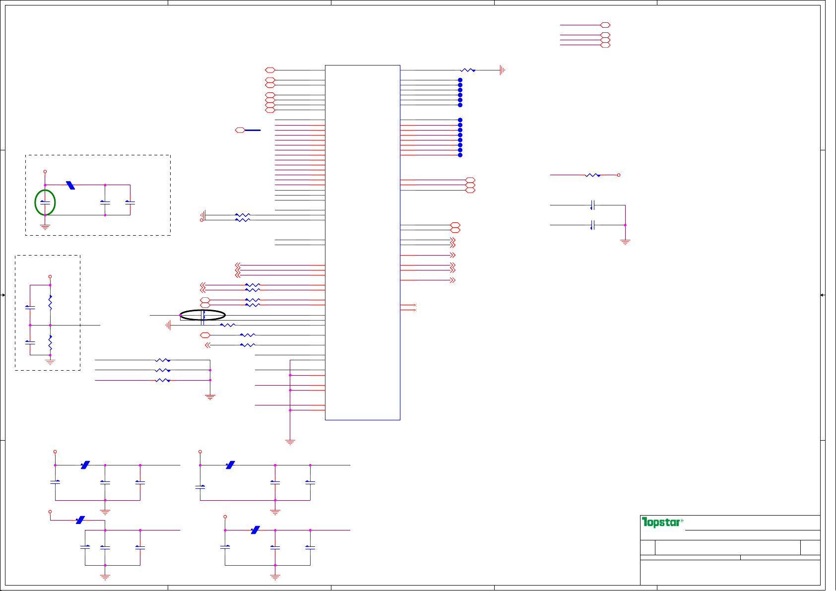
5
hexainf@hotmail.com
GRATIS - FOR FREE
D D
ZAD[0:16]20
+V1.8S
C C
20mA@+1.8V for 671DX estimated
FB39
FB39
1 2
120ohm@100MHz,500mA
120ohm@100MHz,500mA
C107
C107
FB0603
FB0603
10uF/6.3V
10uF/6.3V
Z4XAVDD
C337
C337
Z4XAVSS
0.01uF/25V,X7R
0.01uF/25V,X7R
C340
C340
0.1UF/10V,X7R
0.1UF/10V,X7R
C0402
C0402
Demo SCH: 56ohm,1%
+V1.8S
D13/C12/C13/D15/C15/C14 are left as NC for 671DX!
E12/D11/F12/G12/F11/ are used as Vss for 671DX!
CRT_RED19
+V1.8S
CRT_HSYNC19
CRT_VSYNC19
在
Vzvref=0.45V
NZVREF
CRT_RED
CRT_GREEN
CRT_BLUE
这四个信号都是OD信号,
R131
R131
150,1%
150,1%
C122
C122
0.1UF/10V,X7R
0.1UF/10V,X7R
R0402
R0402
C0402
C0402
R121
R121
C121
C121
0.1UF/10V,X7R
0.1UF/10V,X7R
49.9,1%
49.9,1%
C0402
C0402
R0402
R0402
B B
Connector
CRT_DDC_CLK19
CRT_DDC_DATA19
DACAVDD1 VCOMP
PCI_INTA#9,17,20
CLK14_REF26
R669 150,1%R669 150,1%
R670 150,1%R670 150,1%
R671 150,1%R671 150,1%
CRT_GREEN19
CRT_BLUE19
已经上拉到+
V3.3S
C574 0.1uF/10V,X7RC574 0.1uF/10V,X7R
C573 0.1uF/10V,X7RC573 0.1uF/10V,X7R
R539 130,1%R539 130,1%
NB_ZCLK6
ZDREQ20
ZUREQ20
ZSTB_DP020
ZSTB_DN020
ZSTB_DP120
ZSTB_DN120
R36556.2,1% R0402R36556.2,1% R0402
R12056.2,1% R0402R12056.2,1% R0402
R520 0R520 0
R519 0R519 0
R521 0R521 0
R522 0R522 0
R79 0R79 0
R540 0R540 0
4
MuitIOL Power
WBWN
WREST
CLK14_REF2_R
DACAVDD1
DACAVDD2
DCLKAVDD
ECLKAVDD
ZAD0
ZAD1
ZAD2
ZAD3
ZAD4
ZAD5
ZAD6
ZAD7
ZAD8
ZAD9
ZAD10
ZAD11
ZAD12
ZAD13
ZAD14
ZAD15
ZAD16
NZVREF
NZCOMP
NZCOMP#
Z4XAVDD
Z4XAVSS
AH10
AP8
AN8
AM7
AL7
AP4
AP5
AK10
AM6
AK11
AJ11
AP7
AJ9
AP6
AN6
AK9
AM4
AK6
AK8
AN4
AK7
AL5
AM5
AM8
AL9
AP9
AM9
AM10
AN10
D13
C12
C13
F12
G12
D11
E12
D15
C15
C14
F13
F11
A12
B12
A13
B13
B10
A11
A9
B8
U12A
U12A
ZCLK
ZDREQ
ZUREQ
ZSTB0
ZSTB0#
ZSTB1
ZSTB1#
ZAD0
ZAD1
ZAD2
ZAD3
ZAD4
ZAD5
ZAD6
ZAD7
ZAD8
ZAD9
ZAD10
ZAD11
ZAD12
ZAD13
ZAD14
ZAD15
ZAD16
ZVREF
ZCMP_P
ZCMP_N
Z4XAVDD
Z4XAVSS
ROUT
GOUT
BOUT
HSYNC
VSYNC
VGPIO0
VGPIO1
VCOMP
VVBWN
VRSET
INTA#
VOSCI
DACAVDD1
DACAVSS1
DACAVDD2
DACAVSS2
DCLKAVDD
DCLKAVSS
ECLKAVDD
ECLKAVSS
M672 A1
M672 A1
BGA847
BGA847
F15
ENTEST
TRAP0
TRAP1
TRAP2
TRAP3
TRAP4
TRAP5
TRAP6
TRAP7
TRAP8
TRAP9
TRAP10
AUXOK
PWROK
PCIRST#
VBVSYNC
VBHSYNC
VBHCLK
VBCLK
VBCAD
VACLK
NC0
NC1
D16
E16
F16
D17
E17
F17
AC32
AD34
AB28
AD32
AD33
AE34
AC30
AC29
A5
C6
A7
G14
A6
D8
F7
E7
C8
E9
D9
AH2
AG3
ASL
ASL
TESTMODE0
TESTMODE1
TESTMODE2
AGPSTOP#
AGPBUSY#
VGA DAC Power
VGA DOCK Power
VGA engine Power
3
NB_ENTEST
TM0
TM1
TM2
TRAP0
TRAP1
TRAP2
TRAP3
TRAP4
TRAP5
TRAP6
TRAP7
TRAP8
TRAP9
TRAP10
R70
R70
4.7KR0402
4.7KR0402
ICTP ns
ICTP ns
T24
T24
ICTP ns
ICTP ns
T27
T27
ICTP ns
ICTP ns
T30
T30
ICTP ns
ICTP ns
T25
T25
ICTP ns
ICTP ns
T26
T26
ICTP ns
ICTP ns
T29
T29
Leave as test point!
ICTP ns
ICTP ns
T109
T109
ICTP ns
ICTP ns
T111
T111
ICTP ns
ICTP ns
T37
T37
ICTP ns
ICTP ns
T103
T103
ICTP ns
ICTP ns
T110
T110
ICTP ns
ICTP ns
T112
T112
ICTP ns
ICTP ns
T38
T38
ICTP ns
ICTP ns
T39
T39
AGP_STOP# 21
AGP_BUSY# 21
VBVSYNC 17
VBHSYNC 17
VBHCLK 17
VBCLK 17
VBCAD 17
VACLK 17
ALW_PWROK 21,30,40
NB_PWRGD 30,40
NB_RST# 17,20
AGP_BUSY#
ALW_PWROK
NB_PWRGD
2
R313 4.7K
R313 4.7K
C272
C272
C56
C56
1
+V1.8 6,10,12,14,15,16,36,38,40,41,44
+V1.8S 9,10,12,17,20,21,22,23,38,39,44
+V3.3S 6,7,14,15,17,18,19,20,21,22,23,24,26,27,28,29,31,32,37,38,40,41,42,44
+V1.5S 8,26,28,32,39,40,41
+V3.3S
R0402
R0402
0.1uF/10V,X7R
0.1uF/10V,X7R
C0402
C0402
0.1uF/10V,X7R
0.1uF/10V,X7R
C0402
C0402
+V1.8S
C577
C577
1uF/10V,X7R
1uF/10V,X7R
C0603
C0603
C583
C583
1uF/10V,X7R
1uF/10V,X7R
C0603
C0603
DACAVDD2
10uF/6.3V,X5R
10uF/6.3V,X5R
DACAVDD1
FB55 120ohm/100MHz,500mA
FB55 120ohm/100MHz,500mA
FB0603
FB0603
C575
C575
C0805
C0805
10uF/6.3V,X5R
10uF/6.3V,X5R
A A
+V1.5S
FB60 120ohm/100MHz,500mA
FB60 120ohm/100MHz,500mA
S42C/Delete 1.8v supply.LJ0912
C581
C581
C0805
C0805
10uF/6.3V,X5R
10uF/6.3V,X5R
0.1uF/10V,X7R
0.1uF/10V,X7R
FB0603
FB0603
0.1uF/10V,X7R
0.1uF/10V,X7R
C576
C576
C582
C582
5
C578
C578
C0805
C0805
10uF/6.3V,X5R
10uF/6.3V,X5R
+V1.8S
FB56 120ohm/100MHz,500mA
FB56 120ohm/100MHz,500mA
FB0603
FB0603
+V1.8S
FB58 120ohm/100MHz,500mA
FB58 120ohm/100MHz,500mA
FB0603
FB0603
C584
C584
C0805
C0805
4
C579
C579
0.1uF/10V,X7R
0.1uF/10V,X7R
C585
C585
0.1uF/10V,X7R
0.1uF/10V,X7R
DCLKAVDD
C580
C580
0.01uF/25V,X7R
0.01uF/25V,X7R
ECLKAVDD
C586
C586
0.01uF/25V,X7R
0.01uF/25V,X7R
TOPSTAR TECHNOLOGY
TOPSTAR TECHNOLOGY
TOPSTAR TECHNOLOGY
Echo liu
Echo liu
Page Name
Page Name
Page Name
Size
Size
Size
Project Name Rev
Project Name Rev
Project Name Rev
Custom
Custom
Custom
Date: Sheet
Date: Sheet
Date: Sheet
PROPERTY NOTE: this document contains information confidential and property to
PROPERTY NOTE: this document contains information confidential and property to
PROPERTY NOTE: this document contains information confidential and property to
TOPSTAR and shall not be reproduced or transferred to other documents or disclosed
TOPSTAR and shall not be reproduced or transferred to other documents or disclosed
TOPSTAR and shall not be reproduced or transferred to other documents or disclosed
to others or used for any purpose other than that for which it was obtained without
to others or used for any purpose other than that for which it was obtained without
to others or used for any purpose other than that for which it was obtained without
the expressed written consent of TOPSTAR
the expressed written consent of TOPSTAR
3
2
the expressed written consent of TOPSTAR
Echo liu
Crestline(DMI&CLK)
Crestline(DMI&CLK)
Crestline(DMI&CLK)
S42C
S42C
S42C
1
A
A
A
of
of
of
11 51Saturday, September 27, 2008
11 51Saturday, September 27, 2008
11 51Saturday, September 27, 2008
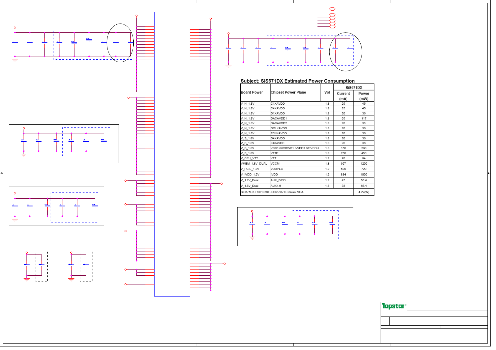
5
+V1.8
667mA@FSB1066+DDR2667
Memory controller Power
Place
C94
C115
C117
C117
C106
C106
10UF/6.3V,X5R
10UF/6.3V,X5R
D D
C0805
C0805
C0603
C0603
1uF/10V,X7R
1uF/10V,X7R
1uF/10V,X7R
1uF/10V,X7R
C115
C102
C102
C0603
C0603
C0603
C0603
1uF/10V,X7R
1uF/10V,X7R
0.1UF/10V,X7R
0.1UF/10V,X7R
Place these capacitors
under 671DX solder side
VCC1.8/VDDVB1.8/PVDDH(Total):
160mA@+1.8V for 671DX estimated
C94
C96
C96
0.1UF/10V,X7R
0.1UF/10V,X7R
C0402
C0402
C0402
C0402 C75
1uF/10V,X7R
1uF/10V,X7R
C471
C471
C114
C114
C0805
C0805
4.7uF/6.3V,X5R
4.7uF/6.3V,X5R
C0603
C0603 C474
+V1.8S
IO driving power
+V1.8S
C C
C95
C95
C103
C103
C0603
10UF/6.3V,X5R
10UF/6.3V,X5R
+V1.2S_PCIE connect to +V1.2S.
timing behind +V1.8S
+V1.2S
C90
C90
10UF/6.3V,X5R
10UF/6.3V,X5R
C0805
C0805
B B
C0603
1uF/10V,X7R
1uF/10V,X7R
C0805
C0805
C74
C74
C0603
C0603
0.1UF/10V,X7R
0.1UF/10V,X7R
1uF/10V,X7R
1uF/10V,X7R
Place these capacitors
under 671DX solder side
+V1.2AL generated from +V1.8AL
+V1.2AL +V1.8AL
C54
C54
C0603
C0603
1uF/10V,X7R
1uF/10V,X7R
1uF/10V,X7R
1uF/10V,X7R
Place these capacitors
under 671DX solder side
0.1UF/10V,X7R
0.1UF/10V,X7R
C82
C82
C0402
C0402
C48
C48
C0603
C0603
C67
C67
C0402
C0402
1uF/10V,X7R
1uF/10V,X7R
Place these capacitors
under 671DX solder side
C125
C125
C0603
C0603
C126
C126
C0603
C0603
1uF/10V,X7R
1uF/10V,X7R
0.1UF/10V,X7R
0.1UF/10V,X7R
IO driving power
Layout note:
将
VDDPEX[0~11]
单独切一
Shape,
与其他
+1.2S连接!
C99
C99
C0603
C0603
1uF/10V,X7R
1uF/10V,X7R
1uF/10V,X7R
1uF/10V,X7R
C92
C92
C0603
C0603
C97
C97
0.1UF/10V,X7R
0.1UF/10V,X7R
C0402
C0402
600mA@+1.2V for 671DX estimated
PXE digital power
C60
C60
C62
C62
C0603
C0603
C0603
1uF/10V,X7R
1uF/10V,X7R
C0603
1uF/10V,X7R
1uF/10V,X7R
C66
C66
C0402
C0402
+V1.8S
IO driving power
+V1.8S
+V1.2S
+V1.2AL
+V1.2AL:38mA
+V1.8AL
+V1.8AL:38mA
+V1.8
C472
C472
C0805
C0805
4.7uF/6.3V,X5R
4.7uF/6.3V,X5R
W23
Y23
AA23
AB23
AC23
AC18
AC20
AC16
AD16
AD17
AD19
AD20
AD21
AD22
AJ22
AJ24
AL23
AL26
AN21
AN23
AN25
AN27
AN29
AP3
AB12
AB13
AC12
AC13
AC14
AC15
AH6
AH7
AN2
AK4
AK5
AL1
AL2
AL3
AL4
AM1
AM2
AM3
AN3
AN5
AN7
AN9
E10
N19
N21
P20
P22
R21
U21
V22
M11
N11
P11
R11
U11
V11
W11
Y11
AA11
AB11
4
AJ4
AJ5
AJ6
AJ7
F10
T22
T11
VCCM_01
VCCM_02
VCCM_03
VCCM_04
VCCM_05
VCCM_06
VCCM_07
VCCM_08
VCCM_09
VCCM_10
VCCM_11
VCCM_12
VCCM_13
VCCM_14
VCCM_15
VCCM_16
VCCM_17
VCCM_18
VCCM_19
VCCM_20
VCCM_21
VCCM_22
VCCM_23
VCC1.8_01
VCC1.8_02
VCC1.8_03
VCC1.8_04
VCC1.8_05
VCC1.8_06
VCC1.8_07
VCC1.8_08
VCC1.8_09
VCC1.8_10
VCC1.8_11
VCC1.8_12
VCC1.8_13
VCC1.8_14
VCC1.8_15
VCC1.8_16
VCC1.8_17
VCC1.8_18
VCC1.8_19
VCC1.8_20
VCC1.8_21
VCC1.8_22
VCC1.8_23
VCC1.8_24
VCC1.8_25
VCC1.8_26
VCC1.8_27
E8
VDDVB1.8_01
F9
VDDVB1.8_02
F8
VDDVB1.8_03
VDD1.8_01
VDD1.8_02
PVDDH_01
PVDDH_02
PVDDH_03
PVDDH_04
PVDDH_05
PVDDH_06
PVDDH_07
PVDDH_08
VDDPEX_01
VDDPEX_02
VDDPEX_03
VDDPEX_04
VDDPEX_05
VDDPEX_06
VDDPEX_07
VDDPEX_08
VDDPEX_09
VDDPEX_10
VDDPEX_11
B5
AUX_IVDD_01
C5
AUX_IVDD_02
D6
AUX_IVDD_03
G8
AUX1.8
U12E
U12E
PWR
PWR
IVDD_01
IVDD_02
IVDD_03
IVDD_04
IVDD_05
IVDD_06
IVDD_07
IVDD_08
IVDD_09
IVDD_10
IVDD_11
IVDD_12
IVDD_13
IVDD_14
IVDD_15
IVDD_16
IVDD_17
IVDD_18
IVDD_19
IVDD_20
IVDD_21
IVDD_22
IVDD_23
IVDD_24
IVDD_25
IVDD_26
IVDD_27
IVDD_28
IVDD_29
IVDD_30
IVDD_31
IVDD_32
IVDD_33
IVDD_34
IVDD_35
IVDD_36
IVDD_37
IVDD_38
IVDD_39
IVDD_40
IVDD_41
IVDD_42
IVDD_43
IVDD_44
IVDD_45
IVDD_46
IVDD_47
IVDD_48
IVDD_49
IVDD_50
IVDD_51
VTT_01
VTT_02
VTT_03
VTT_04
VTT_05
VTT_06
VTT_07
VTT_08
VTT_09
VTT_10
VTT_11
VTT_12
VTT_13
VTT_14
VTT_15
VTT_16
VTT_17
VTT_18
VTT_19
VTT_20
VTT_21
VTT_22
VTT_23
VTT_24
VTT_25
VTT_26
VTT_27
VTTP_01
VTTP_02
VTTP_03
VTTP_04
VTTP_05
VTTP_06
VTTP_07
VTTP_08
VTTP_09
VTTP_10
+V1.2S timing behind +V3.3S
+V1.2S
NB Core Power
M13
M14
M15
M16
M17
M18
M19
N16
N17
N18
N20
R22
N22
N13
P13
Y13
Y22
T13
U13
U22
V13
W13
W22
AA13
AA22
AB14
AB15
AB16
AB18
AB20
AB22
AF6
AF7
AK3
AG4
AG5
AG6
AG7
R13
AH3
AH4
AH5
AJ1
AJ2
AJ3
AK1
AK2
AC22
AC21
AC19
AC17
A19
A20
B19
B20
C19
C20
D19
D20
E19
E20
F19
F20
G19
G20
L18
L19
L20
M20
M21
M22
M23
N23
P23
R23
T23
U23
V23
M12
N12
P12
R12
T12
U12
V12
W12
Y12
AA12
CPU VTT power
IO driving power
+V1.2S
C113
C113
10UF/6.3V,X5R
10UF/6.3V,X5R
C0805
C0805
+V1.05S
+V1.8S
3
IVDD:834mA for 671DX estimated
C69
C69
C0603
C0603
1uF/10V,X7R
1uF/10V,X7R
+V1.05S
10UF/6.3V,X5R
10UF/6.3V,X5R
1uF/10V,X7R
1uF/10V,X7R
C58
C58
C0805
C0805
C64
C64
C65
C65
C0603
C0603
C0603
C0603
1uF/10V,X7R
1uF/10V,X7R
0.1UF/10V,X7R
0.1UF/10V,X7R
1uF/10V,X7R
1uF/10V,X7R
Place these capacitors
under 671DX solder side
C55
C55
C57
C57
C0603
C0603
0.1UF/10V,X7R
0.1UF/10V,X7R
C0402
C0402
Place
C75
C0402
C0402
C72
C72
C63
C63
0.1UF/10V,X7R
0.1UF/10V,X7R
C47
C47
C0603
C0603
1uF/10V,X7R
1uF/10V,X7R
Place these capacitors
under 671DX solder side
C0402
C0402
1uF/10V,X7R
1uF/10V,X7R
C0603
C0603
1uF/10V,X7R
1uF/10V,X7R
C59
C59
0.1UF/10V,X7R
0.1UF/10V,X7R
C0603
C0603
C61
C61
C0402
C0402
2
+V1.8 6,10,14,15,16,36,38,40,41,44
+V1.8S 9,10,11,17,20,21,22,23,38,39,44
+V1.8AL 21,22,23,39,40
+V1.2AL 39,40
+V1.2S 9,37,39,40,41,44
+V1.05S 6,7,8,9,22,23,32,39,40,41,42
C473
C473
C474
C0805
C0805
C0805
C0805
4.7uF/6.3V,X5R
4.7uF/6.3V,X5R
4.7uF/6.3V,X5R
4.7uF/6.3V,X5R
1
A A
5
M672 A1
M672 A1
BGA847
BGA847
4
3
2
Page Name
Page Name
Page Name
Size
Size
Size
Project Name Rev
Project Name Rev
Project Name Rev
A3
A3
A3
Date: Sheet
Date: Sheet
Date: Sheet
PROPERTY NOTE: this document contains information confidential and property to
PROPERTY NOTE: this document contains information confidential and property to
PROPERTY NOTE: this document contains information confidential and property to
TOPSTAR and shall not be reproduced or transferred to other documents or disclosed
TOPSTAR and shall not be reproduced or transferred to other documents or disclosed
TOPSTAR and shall not be reproduced or transferred to other documents or disclosed
to others or used for any purpose other than that for which it was obtained without
to others or used for any purpose other than that for which it was obtained without
to others or used for any purpose other than that for which it was obtained without
the expressed written consent of TOPSTAR
the expressed written consent of TOPSTAR
the expressed written consent of TOPSTAR
TOPSTAR TECHNOLOGY
TOPSTAR TECHNOLOGY
TOPSTAR TECHNOLOGY
Echo liu
Echo liu
Echo liu
Crestline(VSS&NCTF)
Crestline(VSS&NCTF)
Crestline(VSS&NCTF)
S42C
S42C
S42C
1
A
A
A
of
of
of
12 51Saturday, September 27, 2008
12 51Saturday, September 27, 2008
12 51Saturday, September 27, 2008
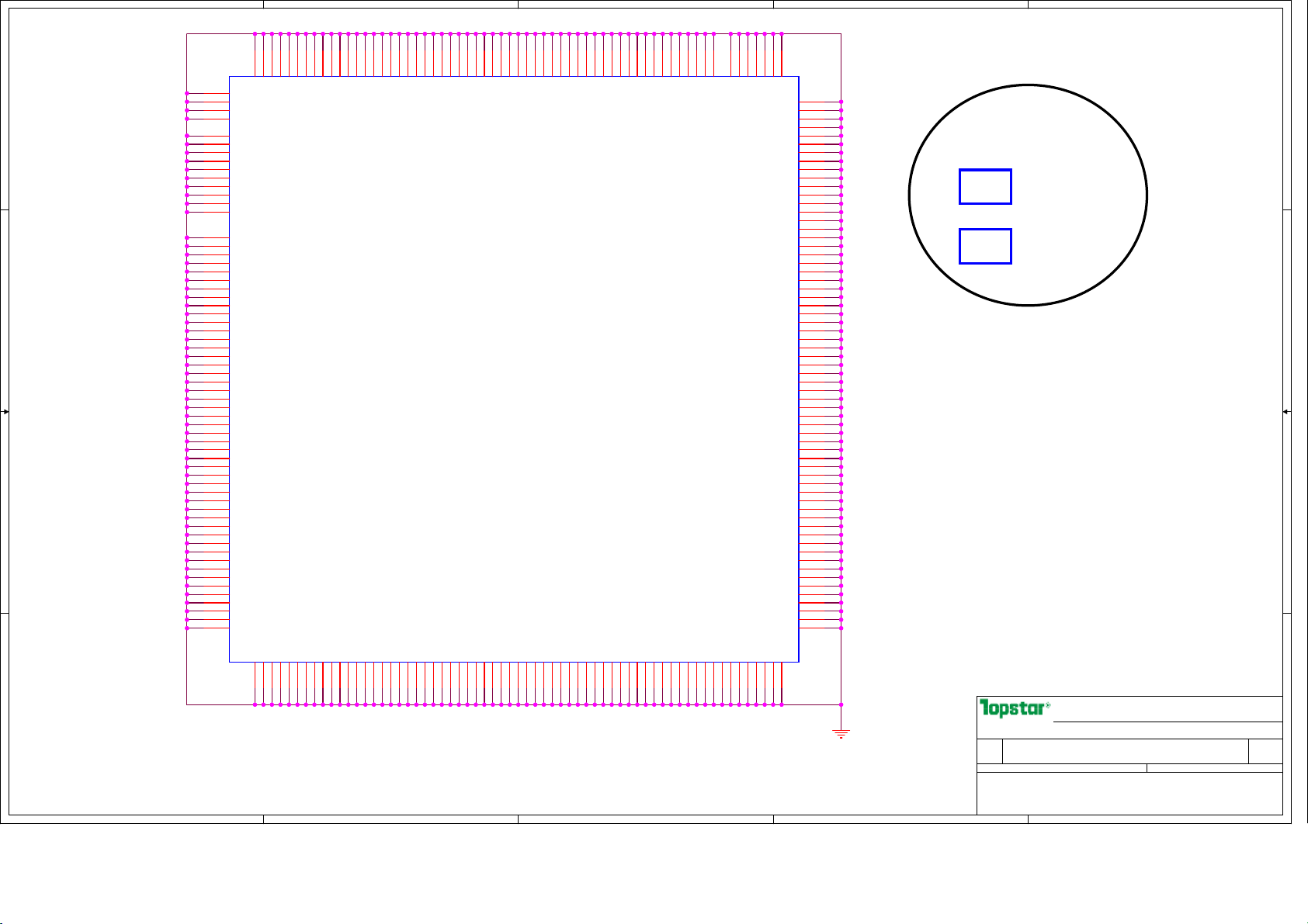
5
hexainf@hotmail.com
GRATIS - FOR FREE
AA16
AA17
AA18
AA19
AA20
AA21
AA31
AA33
AB3
AB4
VSS_192
VSS_193
VSS_194
VSS_195
VSS_06J2VSS_07J3VSS_08J7VSS_09
J31
AB5
VSS_196
VSS_197
VSS_198
VSS_10
VSS_11K3VSS_12K4VSS_13K5VSS_14
J33
U12F
U12F
A3
VSS_64
B2
VSS_65
B3
VSS_188
VSS_189
VSS_190
VSS_01
VSS_02
G31
G33
VSS_03
H4
VSS_191
VSS_04H5VSS_05
H29
D D
C C
B B
A A
5
B4
B21
B23
B25
B27
B29
B31
C1
C2
C3
C4
C9
C10
C11
C16
C18
C32
C33
D1
D2
D3
D4
D5
D10
D12
D21
D23
D25
D27
D29
E1
E2
E3
E6
E11
E13
E14
E18
E29
E30
E33
F2
F3
F4
F5
F6
F14
F22
F24
F26
F28
G2
G3
G7
G10
P21
T21
V21
M672 A1
M672 A1
BGA847
BGA847
VSS_66
VSS_67
VSS_68
VSS_69
VSS_70
VSS_71
VSS_72
VSS_73
VSS_74
VSS_75
VSS_76
VSS_77
VSS_78
VSS_79
VSS_80
VSS_81
VSS_82
VSS_83
VSS_84
VSS_85
VSS_86
VSS_87
VSS_88
VSS_89
VSS_90
VSS_91
VSS_92
VSS_93
VSS_94
VSS_95
VSS_96
VSS_97
VSS_98
VSS_99
VSS_100
VSS_101
VSS_102
VSS_103
VSS_104
VSS_105
VSS_106
VSS_107
VSS_108
VSS_109
VSS_110
VSS_111
VSS_112
VSS_113
VSS_114
VSS_115
VSS_116
VSS_117
VSS_118
VSS_119
VSS_120
VSS_121
VSS_122
VSS_123
VSS_124
AB7
AB29
AC2
VSS_199
VSS_200
K29
AC3
VSS_201
4
AC31
AC33
AD2
AD3
AD4
AD5
AD7
VSS_202
VSS_203
VSS_204
VSS_205
VSS_206
VSS_207
VSS_208
VSS_15L2VSS_16L3VSS_17L4VSS_18L5VSS_19L7VSS_20
VSS_21
L31
L33
4
AD29
AE3
AE31
AE33
VSS_209
VSS_210
VSS_211
VSS_212
VSS_22M2VSS_23M3VSS_24
VSS_25N3VSS_26N4VSS_27N5VSS_28N6VSS_29N7VSS_30
M29
AF2
AF3
VSS_213
VSS_214
VSS_215
GND
GND
AF4
AF5
AF29
VSS_216
VSS_217
N14
N15
AG2
AG31
VSS_219
VSS_220
VSS_218
VSS_31
VSS_32
VSS_33
N31
N33
AG33
AH29
AJ8
AH1
VSS_221
VSS_223
VSS_224
VSS_222
VSS_34P2VSS_35P3VSS_36
VSS_37
P14
P15
AJ10
AJ12
VSS_225
VSS_226
VSS_38
VSS_39
P16
P17
AJ14
AJ16
AJ18
AJ20
VSS_227
VSS_228
VSS_229
VSS_40
VSS_41
VSS_42R2VSS_43R3VSS_44R4VSS_45R5VSS_46
P18
P29
AJ26
AJ28
VSS_230
VSS_231
VSS_232
3
AJ33
AK31
AL6
VSS_233
VSS_234
VSS_47
R14
R15
R16
3
AL8
AL10
VSS_235
VSS_236
VSS_237
VSS_48
VSS_49
VSS_50
R17
R18
AL12
AL14
VSS_238
VSS_239
VSS_51
VSS_52
R19
R20
AL16
AL18
VSS_240
VSS_241
VSS_53
VSS_54
R31
R33
AL20
AL28
AL30
VSS_242
VSS_243
VSS_244
VSS_55T3VSS_56T6VSS_57
VSS_58
T14
T15
AL33
AN11
AN13
VSS_125
VSS_245
VSS_246
VSS_126
VSS_127
VSS_128
VSS_129
VSS_130
VSS_131
VSS_132
VSS_133
VSS_134
VSS_135
VSS_136
VSS_137
VSS_138
VSS_139
VSS_140
VSS_141
VSS_142
VSS_143
VSS_144
VSS_145
VSS_146
VSS_147
VSS_148
VSS_149
VSS_150
VSS_151
VSS_152
VSS_153
VSS_154
VSS_155
VSS_156
VSS_157
VSS_158
VSS_159
VSS_160
VSS_161
VSS_162
VSS_163
VSS_164
VSS_165
VSS_166
VSS_167
VSS_168
VSS_169
VSS_170
VSS_171
VSS_172
VSS_173
VSS_174
VSS_175
VSS_176
VSS_177
VSS_178
VSS_179
VSS_180
VSS_181
VSS_182
VSS_183
VSS_184
VSS_185
VSS_186
VSS_187
VSS_59
VSS_60
T16
T17
T18
AN15
AN17
VSS_247
VSS_248
VSS_249
VSS_61
VSS_62
VSS_63
T19
T20
T29
U2
U3
U4
U5
U6
U14
U15
U16
U17
U18
U19
U20
U31
U33
V2
V3
V4
V5
V14
V15
V16
V17
V18
V19
V20
V29
AN33
AN31
AN19
W3
W14
W15
W16
W17
W18
W19
W20
W21
W31
W33
Y2
Y3
Y4
Y5
Y7
Y14
Y15
Y16
Y17
Y18
Y19
Y20
Y21
Y29
AA2
AA3
AA14
AA15
AB17
AB19
AB21
P19
2
PCB10
PCB10
PCB S42G MB VerA L6 215.14*285.9*1.2 NPB
PCB S42G MB VerA L6 215.14*285.9*1.2 NPB
PCB
PCB
PCB
PCB
PCBA10
PCBA10
PCBA S42G MB VerA NPB
PCBA S42G MB VerA NPB
PCBA
PCBA
PCBA
PCBA
Page Name
Page Name
Page Name
Size
Size
Size
Project Name Rev
Project Name Rev
Project Name Rev
B
B
B
Date: Sheet
Date: Sheet
Date: Sheet
PROPERTY NOTE: this document contains information confidential and property to
PROPERTY NOTE: this document contains information confidential and property to
PROPERTY NOTE: this document contains information confidential and property to
TOPSTAR and shall not be reproduced or transferred to other documents or disclosed
TOPSTAR and shall not be reproduced or transferred to other documents or disclosed
TOPSTAR and shall not be reproduced or transferred to other documents or disclosed
to others or used for any purpose other than that for which it was obtained without
to others or used for any purpose other than that for which it was obtained without
to others or used for any purpose other than that for which it was obtained without
the expressed written consent of TOPSTAR
the expressed written consent of TOPSTAR
2
the expressed written consent of TOPSTAR
Crestline(POWER)
Crestline(POWER)
Crestline(POWER)
S42C
S42C
S42C
1
TOPSTAR TECHNOLOGY
TOPSTAR TECHNOLOGY
TOPSTAR TECHNOLOGY
Echo liu
Echo liu
Echo liu
13 51Saturday, September 27, 2008
13 51Saturday, September 27, 2008
13 51Saturday, September 27, 2008
1
A
A
A
of
of
of
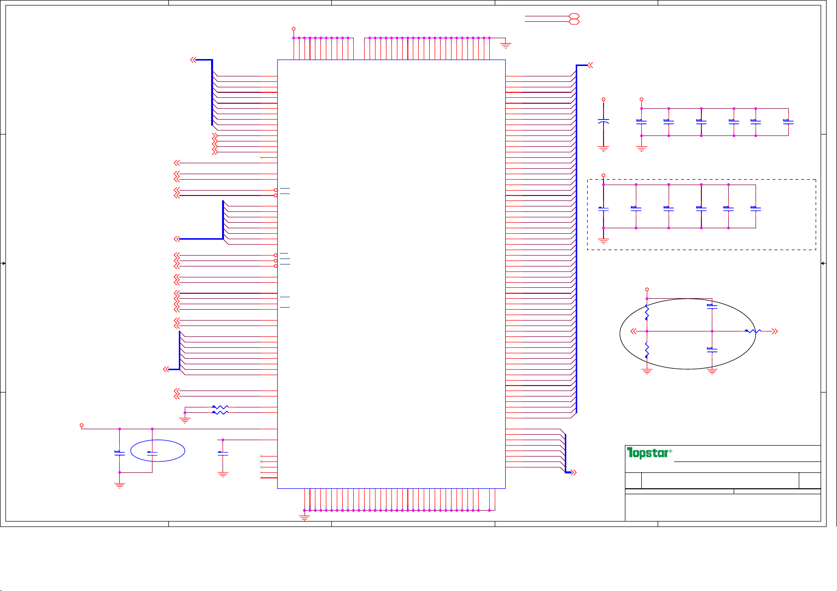
5
4
DIM1
DIM1
DDR2_SODIMM200
+V1.8
DDR2_SODIMM200
DDR200RVS_5D2
DDR200RVS_5D2
3
2
+V3.3S 6,7,11,15,17,18,19,20,21,22,23,24,26,27,28,29,31,32,37,38,40,41,42,44
+V1.8 6,10,12,15,16,36,38,40,41,44
1
112
111
117
118
87
VDD781VDD882VDD9
VSS3
VSS477VSS512VSS648VSS7
183
103
VDD10
VSS878VSS971VSS1072VSS11
184
MA_A_A[10:0]10,15,16
D D
MA_A_A1110,15,16
MA_A_A1210,15,16
MA_A_A1310,15,16
MA_A_A1410,15,16
MA_A_BS#210,15,16
MA_A_BS#010,15,16
MA_A_BS#110,15,16
M_CS#010,16
MEM_CHA_CLK06
MEM_CHA_CLK#06
MEM_CHA_CLK16
MEM_CHA_CLK#16
MA_DM[7:0]10,15
SMB_DATA_S6,15,21,26,28
SMB_CLK_S6,15,21,26,28
M_CS#110,16
MA_A_WE#10,15,16
MA_A_CAS#10,15,16
MA_A_RAS#10,15,16
M_CKE010,16
M_CKE110,16
M_ODT010,16
M_ODT110,16
C173
C173
ns
ns
2.2UF/10V,X7R
2.2UF/10V,X7R
C0805
C0805
MA_DQS0
MA_DQS1
MA_DQS2 MA_DATA50
MA_DQS3
MA_DQS4
MA_DQS5
MA_DQS6
MA_DQS7
C C
B B
MA_DQS[7:0]10,15
Note:
SO-DIMM0 SPD Address is 0xA0
SO-DIMM0 TS Address is 0x30 ??///?????
+V3.3S
0.1UF/25V,Y5V
0.1UF/25V,Y5V
C170
C170
A A
5
C0402
C0402
MA_A_A0
MA_A_A1
MA_A_A2
MA_A_A3
MA_A_A5
MA_A_A6
MA_A_A7
MA_A_A8
MA_A_A9
MA_A_A10
MA_DM0
MA_DM1
MA_DM2
MA_DM3
MA_DM4
MA_DM5
MA_DM6
MA_DM7
R207 10K R0402R207 10K R0402
R206 10K R0402R206 10K R0402
DIMM_VREF_ADIMM_VREF_A
C172
C172
C0603
C0603
1uF/10V,X7R
1uF/10V,X7R
VDD1
VDD2
VDD3
102
A0
101
A1
100
A2
99
A3
98
A4
97
A5
94
A6
92
A7
93
A8
91
A9
105
A10/AP
90
A11
89
A12
116
A13
86
A14
84
A15
85
A16_BA2
107
BA0
106
BA1
110
CS0
115
CS1
10
DQM0
26
DQM1
52
DQM2
67
DQM3
130
DQM4
147
DQM5
170
DQM6
185
DQM7
109
WE
113
CAS
108
RAS
79
CKE0
80
CKE1
30
CK0
32
CK0
164
CK1
166
CK1
114
ODT0
119
ODT1
13
DQS0
31
DQS1
51
DQS2
70
DQS3
131
DQS4
148
DQS5
169
DQS6
188
DQS7
195
SDA
197
SCL
198
SA0
200
SA1
199
VDDSPD
1
VREF1
83
NC1
120
NC2
50
NC3
69
NC4
163
NCTEST
4
VDD496VDD595VDD6
1010 000x
VSS2
VSS1
47
133
190
187
178
VSS36
VSS35
VSS379VSS3821VSS3933VSS40
155
VSS4134VSS42
104
VSS34
VDD1188VDD12
DDRII
VSS12
VSS13
VSS14
VSS158VSS1618VSS1724VSS1841VSS1953VSS2042VSS2154VSS2259VSS2365VSS2460VSS2566VSS26
121
122
196
193
132
144
VSS43
3
156
168
VSS44
VSS45
VSS462VSS473VSS4815VSS4927VSS5039VSS51
127
VSS27
139
VSS28
128
149
161
VSS29
145
165
28
VSS52
VSS53
VSS30
VSS31
171
40
VSS54
VSS32
172
138
VSS55
VSS33
177
150
162
VSS56
DQS#0
DQS#1
DQS#2
DQS#3
DQS#4
DQS#5
DQS#6
DQS#7
201
VSS57
D0
D1
D2
D3
D4
D5
D6
D7
D8
D9
D10
D11
D12
D13
D14
D15
D16
D17
D18
D19
D20
D21
D22
D23
D24
D25
D26
D27
D28
D29
D30
D31
D32
D33
D34
D35
D36
D37
D38
D39
D40
D41
D42
D43
D44
D45
D46
D47
D48
D49
D50
D51
D52
D53
D54
D55
D56
D57
D58
D59
D60
D61
D62
D63
GND0
GND1
202
SO-DIMM 0
MA_DATA0
5
MA_DATA1
7
MA_DATA2
17
MA_DATA3
19
MA_DATA4MA_A_A4
4
MA_DATA5
6
MA_DATA6
14
MA_DATA7
16
MA_DATA8
23
MA_DATA9
25
MA_DATA10
35
MA_DATA11
37
MA_DATA12
20
MA_DATA13
22
MA_DATA14
36
MA_DATA15
38
MA_DATA16
43
MA_DATA17
45
MA_DATA18
55
MA_DATA19
57
MA_DATA20
44
MA_DATA21
46
MA_DATA22
56
MA_DATA23
58
MA_DATA24
61
MA_DATA25
63
MA_DATA26
73
MA_DATA27
75
MA_DATA28
62
MA_DATA29
64
MA_DATA30
74
MA_DATA31
76
MA_DATA32
123
MA_DATA33
125
MA_DATA34
135
MA_DATA35
137
MA_DATA36
124
MA_DATA37
126
MA_DATA38
134
MA_DATA39
136
MA_DATA40
141
MA_DATA41
143
MA_DATA42
151
MA_DATA43
153
MA_DATA44
140
MA_DATA45
142
MA_DATA46
152
MA_DATA47
154
MA_DATA48
157
MA_DATA49
159
173
MA_DATA51
175
MA_DATA52
158
MA_DATA53
160
MA_DATA54
174
MA_DATA55
176
MA_DATA56
179
MA_DATA57
181
MA_DATA58
189
MA_DATA59
191
MA_DATA60
180
MA_DATA61
182
MA_DATA62
192
MA_DATA63
194
MA_DQS#0
11
MA_DQS#1
29
MA_DQS#2
49
MA_DQS#3
68
MA_DQS#4
129
MA_DQS#5
146
MA_DQS#6
167
MA_DQS#7
186
MA_DATA[63:0] 10,15
Change into 0.1uF CAP. x4 and 470uF x1 Per DIMM
+V1.8
12
C178
C178
1
1
+
+
CT7343_19
CT7343_19
220UF/2.5V,POSCAP
220UF/2.5V,POSCAP
+V1.8
C165
C165
C0805
C0805
2.2UF/10V,X7R
2.2UF/10V,X7R
ns
ns
0.1UF/25V,Y5V
0.1UF/25V,Y5V
+V1.8
C625
C625
C0402
C0402
0.1UF/25V,Y5V
0.1UF/25V,Y5V
C163
C163
C0402
C0402
C626
C626
C0402
C0402
0.1UF/25V,Y5V
0.1UF/25V,Y5V
C166
C166
C0402
C0402
0.1UF/25V,Y5V
0.1UF/25V,Y5V
C627
C627
C0402
C0402
0.1UF/25V,Y5V
0.1UF/25V,Y5V
C208
C208
C0402
C0402
0.1UF/25V,Y5V
0.1UF/25V,Y5V
C628
C628
C0402
C0402
0.1UF/25V,Y5V
0.1UF/25V,Y5V
C179
C179
C0402
C0402
0.1UF/25V,Y5V
0.1UF/25V,Y5V
C629
C629
C0402
C0402
0.1UF/25V,Y5V
0.1UF/25V,Y5V
C171
C171
C0402
C0402
0.1UF/25V,Y5V
0.1UF/25V,Y5V
0.1UF/25V,Y5V
0.1UF/25V,Y5V
Layout note:电容靠近DDR slot VDD PIN
Note:
+V1.8
C190
R213
R213
1K,1%
1K,1%
R0402
R0402
ns
ns
DIMM_VREF_A15 SM_VREF 10,36
DIMM_VREF_A
R214
R214
1K,1%
1K,1%
R0402
R0402
ns
ns
C190
0.1UF/25V,Y5V
0.1UF/25V,Y5V
C0402
C0402
C191
C191
0.1UF/25V,Y5V
0.1UF/25V,Y5V
C0402
C0402
close to DDR pin
Page Name
Page Name
MA_DQS#[7:0] 10,15
2
Page Name
Size
Size
Size
Project Name Rev
Project Name Rev
Project Name Rev
B
B
B
Date: Sheet
Date: Sheet
Date: Sheet
PROPERTY NOTE: this document contains information confidential and property to
PROPERTY NOTE: this document contains information confidential and property to
PROPERTY NOTE: this document contains information confidential and property to
TOPSTAR and shall not be reproduced or transferred to other documents or disclosed
TOPSTAR and shall not be reproduced or transferred to other documents or disclosed
TOPSTAR and shall not be reproduced or transferred to other documents or disclosed
to others or used for any purpose other than that for which it was obtained without
to others or used for any purpose other than that for which it was obtained without
to others or used for any purpose other than that for which it was obtained without
the expressed written consent of TOPSTAR
the expressed written consent of TOPSTAR
the expressed written consent of TOPSTAR
Selected by layout to seperated from
other sensitive signal trace.
0
0
R209
R209
R0603
R0603
TOPSTAR TECHNOLOGY
TOPSTAR TECHNOLOGY
TOPSTAR TECHNOLOGY
Echo liu
Echo liu
Echo liu
DDRII SODIMM0
DDRII SODIMM0
DDRII SODIMM0
S42C
S42C
S42C
of
of
of
14 51Saturday, September 27, 2008
14 51Saturday, September 27, 2008
14 51Saturday, September 27, 2008
1
C630
C630
C0402
C0402
A
A
A
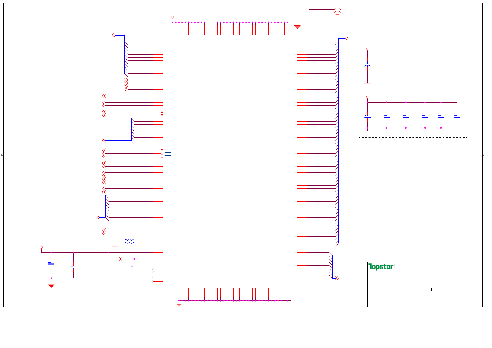
5
hexainf@hotmail.com
GRATIS - FOR FREE
4
DIM2
DIM2
DDR2_SODIMM200
+V1.8
DDR2_SODIMM200
DDR200RVS_9D2C
DDR200RVS_9D2C
3
2
+V3.3S 6,7,11,14,17,18,19,20,21,22,23,24,26,27,28,29,31,32,37,38,40,41,42,44
+V1.8 6,10,12,14,16,36,38,40,41,44
1
150
162
VSS56
DQS#0
DQS#1
DQS#2
DQS#3
DQS#4
DQS#5
DQS#6
DQS#7
201
VSS57
D0
D1
D2
D3
D4
D5
D6
D7
D8
D9
D10
D11
D12
D13
D14
D15
D16
D17
D18
D19
D20
D21
D22
D23
D24
D25
D26
D27
D28
D29
D30
D31
D32
D33
D34
D35
D36
D37
D38
D39
D40
D41
D42
D43
D44
D45
D46
D47
D48
D49
D50
D51
D52
D53
D54
D55
D56
D57
D58
D59
D60
D61
D62
D63
GND0
GND1
202
SO-DIMM 1
MA_DATA0
5
MA_DATA1
7
MA_DATA2
17
MA_DATA3
19
MA_DATA4MA_A_A4
4
MA_DATA5
6
MA_DATA6
14
MA_DATA7
16
MA_DATA8
23
MA_DATA9
25
MA_DATA10
35
MA_DATA11
37
MA_DATA12
20
MA_DATA13
22
MA_DATA14
36
MA_DATA15
38
MA_DATA16
43
MA_DATA17
45
MA_DATA18
55
MA_DATA19
57
MA_DATA20
44
MA_DATA21
46
MA_DATA22
56
MA_DATA23
58
MA_DATA24
61
MA_DATA25
63
MA_DATA26
73
MA_DATA27
75
MA_DATA28
62
MA_DATA29
64
MA_DATA30
74
MA_DATA31
76
MA_DATA32
123
MA_DATA33
125
MA_DATA34
135
MA_DATA35
137
MA_DATA36
124
MA_DATA37
126
MA_DATA38
134
MA_DATA39
136
MA_DATA40
141
MA_DATA41
143
MA_DATA42
151
MA_DATA43
153
MA_DATA44
140
MA_DATA45
142
MA_DATA46
152
MA_DATA47
154
MA_DATA48
157
MA_DATA49
159
173
MA_DATA51
175
MA_DATA52
158
MA_DATA53
160
MA_DATA54
174
MA_DATA55
176
MA_DATA56
179
MA_DATA57
181
MA_DATA58
189
MA_DATA59
191
MA_DATA60
180
MA_DATA61
182
MA_DATA62
192
MA_DATA63
194
MA_DQS#0
11
MA_DQS#1
29
MA_DQS#2
49
MA_DQS#3
68
MA_DQS#4
129
MA_DQS#5
146
MA_DQS#6
167
MA_DQS#7
186
MA_DATA[63:0] 10,14
2.2UF/10V,X7R
2.2UF/10V,X7R
MA_DQS#[7:0] 10,14
2
+V1.8
12
C167
C167
1
1
+
+
CT7343_19
CT7343_19
220UF/2.5V,POSCAP
220UF/2.5V,POSCAP
+V1.8
C209
C210
C210
DIMM2
DIMM2
C0805
C0805
C162
C162
DIMM2
DIMM2
C0402
C0402
0.1UF/25V,Y5V
0.1UF/25V,Y5V
C134
C134
DIMM2
DIMM2
C0402
C0402
0.1UF/25V,Y5V
0.1UF/25V,Y5V
0.1UF/25V,Y5V
0.1UF/25V,Y5V
C164
C164
DIMM2
DIMM2
C0402
C0402
C209
DIMM2
DIMM2
C0402
C0402
0.1UF/25V,Y5V
0.1UF/25V,Y5V
C207
C207
DIMM2
DIMM2
C0402
C0402
0.1UF/25V,Y5V
0.1UF/25V,Y5V
Layout note:电容靠近DDR slot VDD PIN
TOPSTAR TECHNOLOGY
TOPSTAR TECHNOLOGY
TOPSTAR TECHNOLOGY
Echo liu
Echo liu
Page Name
Page Name
Page Name
Size
Size
Size
Project Name Rev
Project Name Rev
Project Name Rev
B
B
B
Date: Sheet
Date: Sheet
Date: Sheet
PROPERTY NOTE: this document contains information confidential and property to
PROPERTY NOTE: this document contains information confidential and property to
PROPERTY NOTE: this document contains information confidential and property to
TOPSTAR and shall not be reproduced or transferred to other documents or disclosed
TOPSTAR and shall not be reproduced or transferred to other documents or disclosed
TOPSTAR and shall not be reproduced or transferred to other documents or disclosed
to others or used for any purpose other than that for which it was obtained without
to others or used for any purpose other than that for which it was obtained without
to others or used for any purpose other than that for which it was obtained without
the expressed written consent of TOPSTAR
the expressed written consent of TOPSTAR
the expressed written consent of TOPSTAR
Echo liu
DDRII SODIMM0
DDRII SODIMM0
DDRII SODIMM0
S42C
S42C
S42C
15 51Saturday, September 27, 2008
15 51Saturday, September 27, 2008
15 51Saturday, September 27, 2008
of
of
of
1
A
A
A
VSS27
139
VSS28
128
149
161
VSS29
145
165
28
VSS52
VSS53
VSS30
VSS31
171
40
VSS54
VSS32
172
138
VSS55
VSS33
177
112
111
117
118
87
VDD781VDD882VDD9
VSS3
VSS477VSS512VSS648VSS7
183
103
VDD10
VSS878VSS971VSS1072VSS11
184
MA_A_A[10:0]10,14,16
D D
MA_A_A1110,14,16
MA_A_A1210,14,16
MA_A_A1310,14,16
MA_A_A1410,14,16
MA_A_BS#210,14,16
MA_A_BS#010,14,16
MA_A_BS#110,14,16
M_CS#210,16
C C
B B
MA_DQS[7:0]10,14
Note:
SO-DIMM1 SPD Address is 0xA2
+V3.3S
SO-DIMM1 TS Address is 0x3X ????////??
0.1UF/25V,Y5V
0.1UF/25V,Y5V
C189
C189
DIMM2
DIMM2
C0402
A A
C0402
5
M_CS#310,16
MA_DM[7:0]10,14
MA_A_WE#10,14,16
MA_A_CAS#10,14,16
MA_A_RAS#10,14,16
M_CKE210,16
M_CKE310,16
MEM_CHA_CLK26
MEM_CHA_CLK#26
MEM_CHA_CLK36
MEM_CHA_CLK#36
M_ODT210,16
M_ODT310,16
SMB_DATA_S6,14,21,26,28
SMB_CLK_S6,14,21,26,28
C183
C183
ns/DIMM2
ns/DIMM2
2.2UF/10V,X7R
2.2UF/10V,X7R
C0805
C0805
MA_DQS0
MA_DQS1
MA_DQS2 MA_DATA50
MA_DQS3
MA_DQS4
MA_DQS5
MA_DQS6
MA_DQS7
DIMM_VREF_A14
R438 10K R0402DIMM2 R438 10K R0402DIMM2
R439 10K R0402DIMM2 R439 10K R0402DIMM2
MA_A_A0
MA_A_A1
MA_A_A2
MA_A_A3
MA_A_A5
MA_A_A6
MA_A_A7
MA_A_A8
MA_A_A9
MA_A_A10
MA_DM0
MA_DM1
MA_DM2
MA_DM3
MA_DM4
MA_DM5
MA_DM6
MA_DM7
DIMM_VREF_A
C188
C188
DIMM2
DIMM2
C0603
C0603
1uF/10V,X7R
1uF/10V,X7R
VDD1
VDD2
VDD3
102
A0
101
A1
100
A2
99
A3
98
A4
97
A5
94
A6
92
A7
93
A8
91
A9
105
A10/AP
90
A11
89
A12
116
A13
86
A14
84
A15
85
A16_BA2
107
BA0
106
BA1
110
CS0
115
CS1
10
DQM0
26
DQM1
52
DQM2
67
DQM3
130
DQM4
147
DQM5
170
DQM6
185
DQM7
109
WE
113
CAS
108
RAS
79
CKE0
80
CKE1
30
CK0
32
CK0
164
CK1
166
CK1
114
ODT0
119
ODT1
13
DQS0
31
DQS1
51
DQS2
70
DQS3
131
DQS4
148
DQS5
169
DQS6
188
DQS7
195
SDA
197
SCL
198
SA0
200
SA1
199
VDDSPD
1
VREF1
83
NC1
120
NC2
50
NC3
69
NC4
163
NCTEST
4
VDD496VDD595VDD6
1010 001x
VSS2
VSS1
47
133
190
104
187
178
155
VSS36
VSS34
VSS35
VSS379VSS3821VSS3933VSS40
VDD1188VDD12
VSS4134VSS42
DDRII
VSS12
VSS13
VSS14
VSS158VSS1618VSS1724VSS1841VSS1953VSS2042VSS2154VSS2259VSS2365VSS2460VSS2566VSS26
121
122
196
193
132
144
VSS43
3
156
168
VSS44
VSS45
VSS462VSS473VSS4815VSS4927VSS5039VSS51
127
DIMM2
DIMM2
5
4
3
2
+V0.9S 36,41
+V1.8 6,10,12,14,15,36,38,40,41,44
1
D D
+V0.9S
C C
B B
A A
5
RA0402_8
RA0402_8
56x4
56x4
1 2
3 4
5 6
7 8
RN19
RN19
RN20 56x4 RA0402_8RN20 56x4 RA0402_8
1 2
3 4
5 6
7 8
RN14 56x4 RA0402_8RN14 56x4 RA0402_8
1 2
3 4
5 6
7 8
RN18 56x4 RA0402_8RN18 56x4 RA0402_8
1 2
3 4
5 6
7 8
1 2
3 4
5 6
7 8
RN17 56x4 RA0402_8RN17 56x4 RA0402_8
RN16 56x4 RA0402_8RN16 56x4 RA0402_8
1 2
3 4
5 6
7 8
RN13 56x4 RA0402_8RN13 56x4 RA0402_8
1 2
3 4
5 6
7 8
RN15 56x4 RA0402_8RN15 56x4 RA0402_8
1 2
3 4
5 6
7 8
R212 56 R0402R212 56 R0402
MA_A_A12
MA_A_BS#2
MA_A_BS#0
MA_A_A10
MA_A_A3
MA_A_BS#1
MA_A_A13
MA_A_A1
MA_A_A5
MA_A_A8
MA_A_A9
MA_A_A6
MA_A_A4
MA_A_A2
MA_A_A0
MA_A_A14
MA_A_A11
MA_A_A7
M_CS#2 10,15
MA_A_RAS# 10,14,15
M_ODT2 10,15
M_ODT1 10,14
M_ODT0 10,14
M_CS#1 10,14
M_CKE3 10,15
M_CS#3 10,15
M_ODT3 10,15
MA_A_CAS# 10,14,15
M_CS#0 10,14
M_CKE0 10,14
M_CKE1 10,14
MA_A_WE# 10,14,15
M_CKE2 10,15
4
+V0.9S
C195
C195
0.1UF/25V,Y5V
0.1UF/25V,Y5V
C0402
C0402
+V0.9S
C184
C184
0.1UF/25V,Y5V
0.1UF/25V,Y5V
C0402
C0402
+V1.8
+V0.9S
C502
C502
0.1UF/25V,Y5V
0.1UF/25V,Y5V
C0402
C0402
+V1.8
每4个电阻两个
C193
C200
C200
0.1UF/25V,Y5V
0.1UF/25V,Y5V
C0402
C0402
C181
C181
0.1UF/25V,Y5V
0.1UF/25V,Y5V
C0402
C0402
C501
C501
0.1UF/25V,Y5V
0.1UF/25V,Y5V
C0402
C0402
C193
0.1UF/25V,Y5V
0.1UF/25V,Y5V
C0402
C0402
C187
C187
0.1UF/25V,Y5V
0.1UF/25V,Y5V
C0402
C0402
C500
C500
0.1UF/25V,Y5V
0.1UF/25V,Y5V
C0402
C0402
0.1UF
C199
C199
0.1UF/25V,Y5V
0.1UF/25V,Y5V
C0402
C0402
C175
C175
0.1UF/25V,Y5V
0.1UF/25V,Y5V
C0402
C0402
电容
Layout note:
1.Place one cap every 2 terminated resistors;
2.Place +V1.8 to +V0.9 Caps by their power shape;
3.BOM costdown by layout or by test.
MA_A_A[10:0]10,14,15
MA_A_BS#010,14,15
MA_A_BS#110,14,15
MA_A_BS#210,14,15
MA_A_A1110,14,15
MA_A_A1210,14,15
MA_A_A1310,14,15
MA_A_A1410,14,15
3
Page Name
Page Name
Page Name
Size
Size
Size
A4
A4
A4
Date: Sheet
Date: Sheet
Date: Sheet
PROPERTY NOTE: this document contains information confidential and property to
PROPERTY NOTE: this document contains information confidential and property to
PROPERTY NOTE: this document contains information confidential and property to
TOPSTAR and shall not be reproduced or transferred to other documents or disclosed
TOPSTAR and shall not be reproduced or transferred to other documents or disclosed
TOPSTAR and shall not be reproduced or transferred to other documents or disclosed
to others or used for any purpose other than that for which it was obtained without
to others or used for any purpose other than that for which it was obtained without
to others or used for any purpose other than that for which it was obtained without
the expressed written consent of TOPSTAR
the expressed written consent of TOPSTAR
the expressed written consent of TOPSTAR
2
C198
C192
C201
C194
C194
0.1UF/25V,Y5V
0.1UF/25V,Y5V
C0402
C0402
C174
C174
0.1UF/25V,Y5V
0.1UF/25V,Y5V
C0402
C0402
Project Name Rev
Project Name Rev
Project Name Rev
C201
0.1UF/25V,Y5V
0.1UF/25V,Y5V
C0402
C0402
C186
C186
0.1UF/25V,Y5V
0.1UF/25V,Y5V
C0402
C0402
TOPSTAR TECHNOLOGY
TOPSTAR TECHNOLOGY
TOPSTAR TECHNOLOGY
Echo liu
Echo liu
Echo liu
DDRII Series Termination
DDRII Series Termination
DDRII Series Termination
S42C
S42C
S42C
C192
0.1UF/25V,Y5V
0.1UF/25V,Y5V
C0402
C0402
C185
C185
0.1UF/25V,Y5V
0.1UF/25V,Y5V
C0402
C0402
C198
C0805
C0805
4.7uF/10V,X5R
4.7uF/10V,X5R
16 51Saturday, September 27, 2008
16 51Saturday, September 27, 2008
16 51Saturday, September 27, 2008
1
4.7uF/10V,X5R
4.7uF/10V,X5R
of
of
of
C202
C202
C0805
C0805
A
A
A
 Loading...