

Page 1
TP6312
1/4 TO 1/11-DUTY VFD CONTROLLER/DRIVER
General Description
The TP6312 is a VFD (Vacuum Fluorescent Display)
controller/driver that is driven on a 1/4 to 1/11-duty
factor. It consists of 11 segment output lines, 6 grid
output lines, 5 segment/grid output drivelines, a
display memory, a control circuit, and a Key scan
circuit. Serial data is input to TP6312 through a
three-line serial interface. This VFD controller/driver
is ideal as a peripheral device of a single-chip
microcomputer.
Ordering Information
TP 6312
Footprint
Version
Package Type
Features
Multiple display modes (11-segment & 11-digit to
16-segment & 4-digit)
Key scanning (6 × 4 matrices)
Dimming circuit (eight steps)
High-voltage output (V
LED ports (4 chs, 20 mA max)
General-purpose input port (4 bits)
No external resistor necessary for driver outputs
(P-ch open-drain + pull-down resistor output)
Serial interface (CLK, STB, D
Package Type
Footprint
F: LQFP
S: 2.0 mm
L: 3.2 mm
– 35V max)
DD
IN
, D
OUT
)
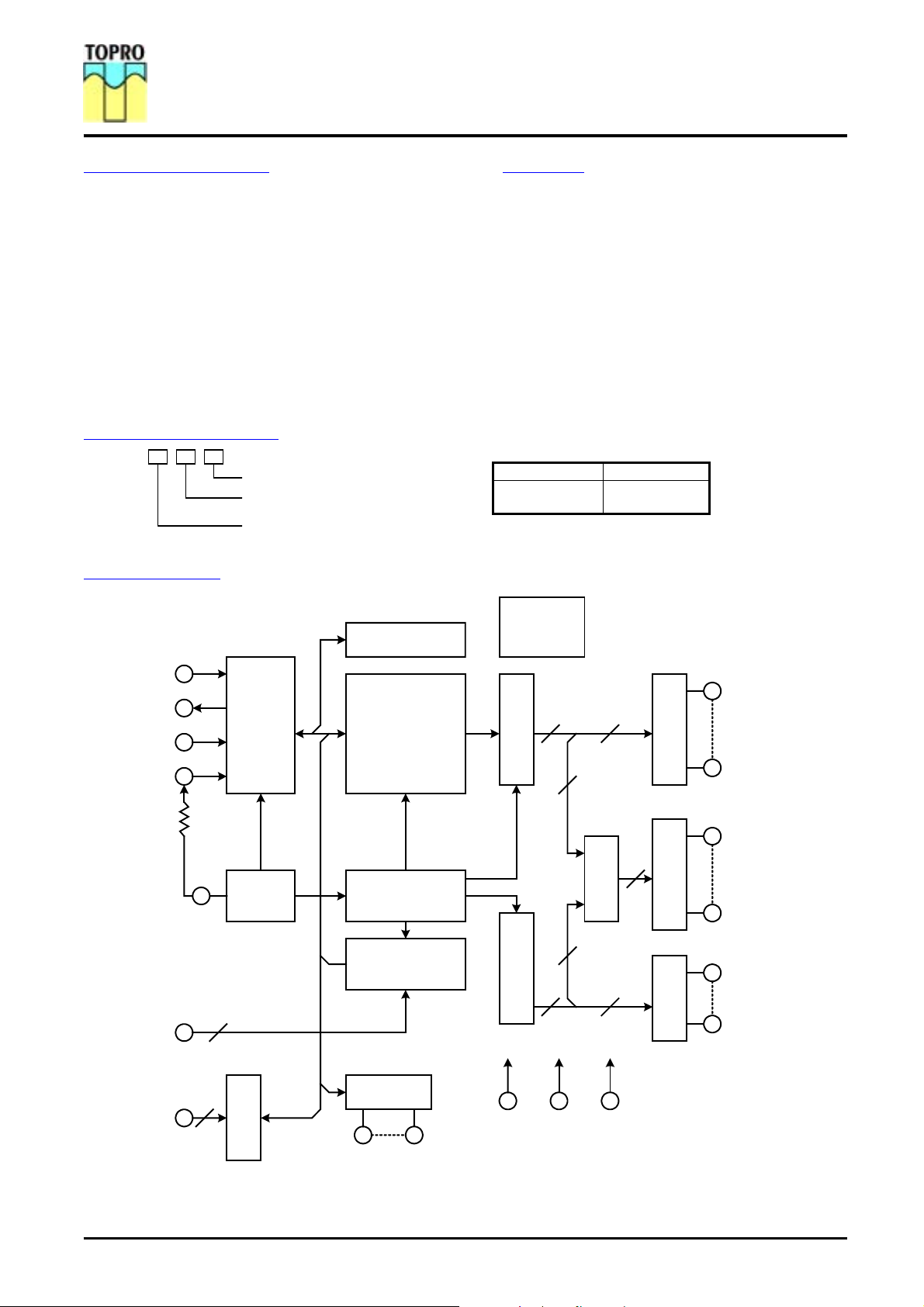
Block Diagram
DIN
DOUT
CLK
STB
R
Key1
to
Key4
4
Serial I/F
OSC
Command decoder
Display memory
16bit x 11 word
Timing generator key
scan
Key data memory
(4x6)
Dimming circuit
16 11
16-bit output latch16-bit output latch
11 6
Seg1
Segment driverSegment/grid driverGrid driver
5
5
Data selector
5
Seg11
Seg12/Gird11
Seg16/Gird7
Grid1
Grid6
SW1
to
SW4
4
4 bit latch
4 bit latch
1
LED
LED
VDD VSS VEE
(+5V) (0V) (-30V)
4
Version 1.1 Page 1 of 9 http://www.topro.com.tw
September 2003
Page 2
TP6312
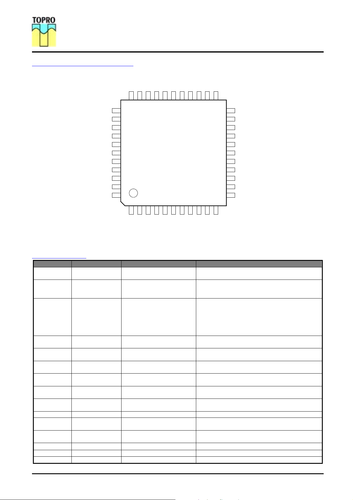
Pin Configuration (Top View)
Grid 4
Grid 3
Grid 2
Grid 1
DD
V
LED 4
LED 3
LED 2
LED 1
VSS
OSC
44 43 42 41 40 39 38 37 36 35 34
Use all the power pins.
1/4 TO 1/11-DUTY VFD CONTROLLER/DRIVER
EE
Grid 6
Grid 5
33
1
SW 1
Seg15 / Grid 8
Seg16 / Grid 7
30
31
32
2
3
4
SW 2
SW 3
SW 4
V
Seg14 / Grid 9
Seg13 / Grid 10
Seg12 / Grid 11
26
27
28
29
5
6
7
8
OUT
DIN
CLK
VSS
D
Seg9
Seg10
Seg11
23
24
25
Seg8
Seg7
Seg6 / KS6
Seg5 / KS5
Seg4 / KS4
Seg3 / KS3
Seg2 / KS2
Seg1 / KS1
V
DD
KEY 4
KEY 3
12 13 14 15 16 17 18 19 20 21 22
9
10
11
STB
KEY 1
KEY 2
Pin Description
Pin No Symbol Pin Name Description
6 DIN Date input
5 D
Date output
OUT
9 STB Strobe
8 CLK Clock input
44 OSC Oscillator pin
/KS1 to
Seg
Seg
Seg
1
Seg
6
/Grid11 to
11
16
/KS6
/Grid7
High-voltage output
High-voltage output
(Segment)
High-voltage output
(Grid)
High-voltage output
(Segment/grid)
15 to 20
21 to 25 Seg7 to Seg11
37 to 32 Grid1 to Grid6
26, 28 to 31
42 to 39 LED1 to LED4 LED output CMOS output. +20 mA max.
10 to 13 Key1 to Key4 Key data input
1 to 4 SW1 to SW4 Switch input
14, 38 VDD Logic power
7, 43 VSS Logic ground Connect this pin to system GND.
27 VEE Pull-down level VDD – 35 V max
Inputs serial data at rising edge of shift clock,
starting from the lower bit.
Outputs serial data at falling edge of shift clock,
starting from the lower bit. This is N-ch open-drain
output pin.
Initializes the serial interface at rising or falling edge
to make TP6312 waiting for reception of command.
Data input after STB has fallen is processed as
command. While command data is processed,
current processing is stopped and serial interface is
initialized. While STB is high, CLK is ignored.
Reads serial data at rising edge, and outputs data at
falling edge.
Connects a resistor to this pin to determine the
oscillation frequency to this pin.
Segment output pins (Dual function as Key source).
Segment output pins.
Grid output pins.
These pins are selectable for segment or grid
driving.
Data input to these pins is latched at the end of
display cycle.
These pins constitute 4-bit general-purpose input
port.
5V ± 10%
Version 1.1 Page 2 of 9 http://www.topro.com.tw
September 2003
Page 3
TP6312
1/4 TO 1/11-DUTY VFD CONTROLLER/DRIVER
Functional Description
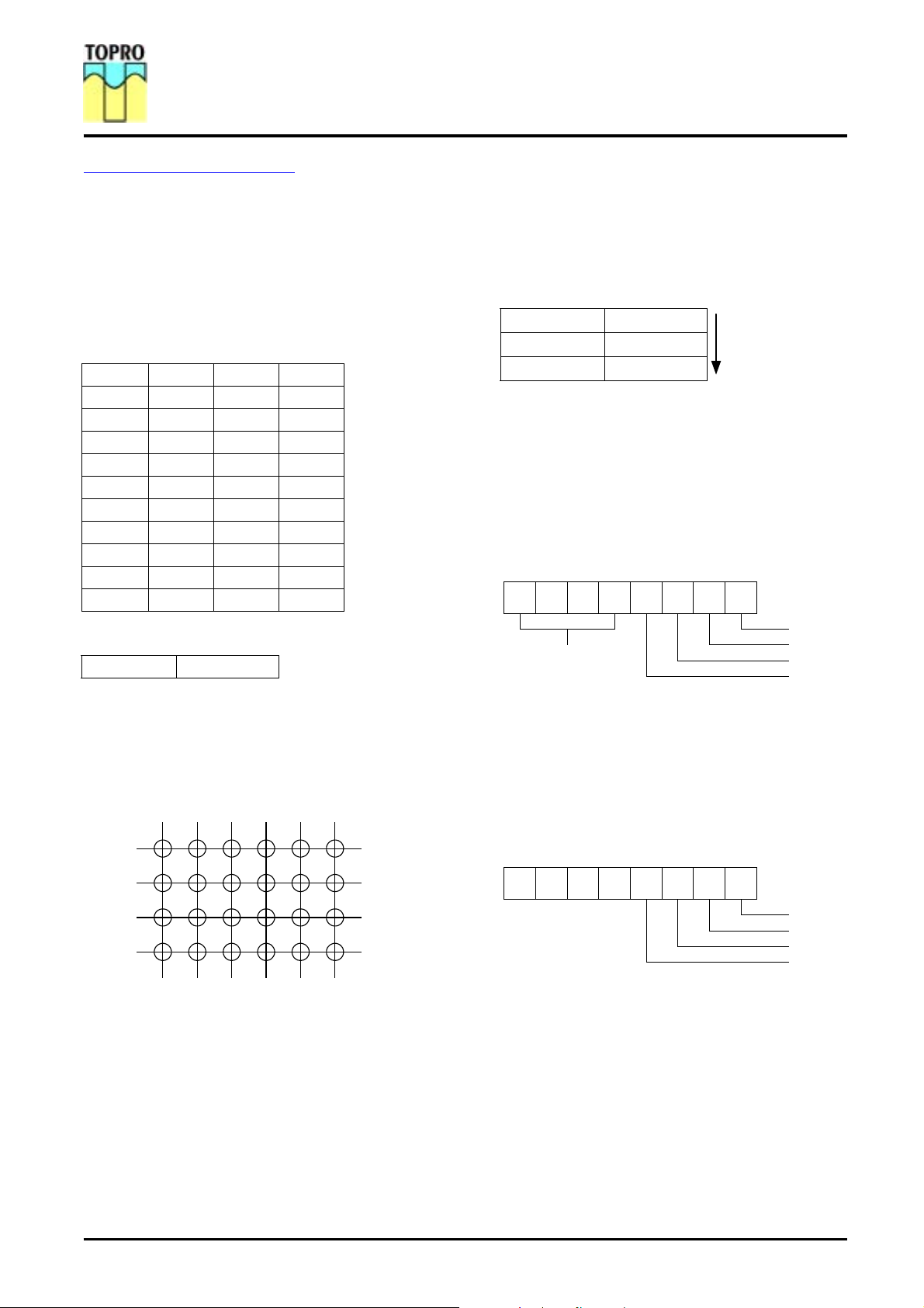
Display RAM Address and Display Mode
The display RAM stores the data transmitted from an
external device to TP6312 through the serial interface,
and is assigned addresses as follows, in units of 8
bits:
Seg
Seg4 Seg8 Seg
1
00HU 01HL 01HU DIG1
00H
L
02HL 02HU 03HL 03HU DIG2
04HL 04HU 05HL 05HU DIG3
06HL 06HU 07HL 07HU DIG4
08HL 08HU 09HL 09HU DIG5
0AHL 0AHU 0BHL 0BHU DIG6
0CHL 0CHU 0DHL 0DHU DIG7
0EHL 0EHU 0FHL 0FHU DIG8
10HL 10HU 11HL 11HU DIG9
12HL 12HU 13HL 13HU DIG10
14HL 14HU 15HL 15HU DIG11
b
b
0
b
3 b4
7
XX HL XX HU
Lower 4 bits Higher 4 bits.
12
Seg16
Key Matrix and Key-Input Data Storage
RAM
The Key matrix is of 6 × 4 configuration, as shown
below.
KEY1
KEY2
The data of each Key is stored as illustrated below,
and is read by a read command, starting from the
least significant bit.
Key
Key4Key1 Key4
1
/ KS1 Seg2 / KS2
Seg
1
Seg3 / KS3 Seg4 / KS4
Reading s eque nce
Seg5 / KS5 Seg6 / KS6
b0 b3 b4 b7
LED Port
Data is written to the LED port by a write command,
starting from the least significant bit of the port.
When a bit of this port is 0, the corresponding LED
lights; when the bit is 1, the LED goes off. The data
of bits 5 through 8 is ignored.
---- ---- ---- ---- b3 b2 b1 b0
LED1
Don't care
LED2
LED3
LED4
On power application, all LEDs are unlit.
SW Data
The SW data is read by a read command, starting
from the least significant bit. Bits 5 through 8 of the
SW data are 0.
MSB LSB
0 0 0 0 b3 b2 b1 b0
KEY3
KEY4
SW1
SW2
SW3
SW4
Commands
Seg1/KS1
Seg2/KS2
Seg3/KS3
Seg4/KS4
Seg5/KS5
Seg6/KS6
A command sets the display mode and status of the
VFD driver.
The first 1 byte input to TP6312 through the D
IN
pin
after the STB pin has fallen is regarded as a
command.
If STB is high while a command/data is transmitted,
serial communication is initialized, and the
transmitting command/data is invalid; however, the
Version 1.1 Page 3 of 9 http://www.topro.com.tw
September 2003
Page 4
TP6312
1/4 TO 1/11-DUTY VFD CONTROLLER/DRIVER
command/data already transmitted remains valid.
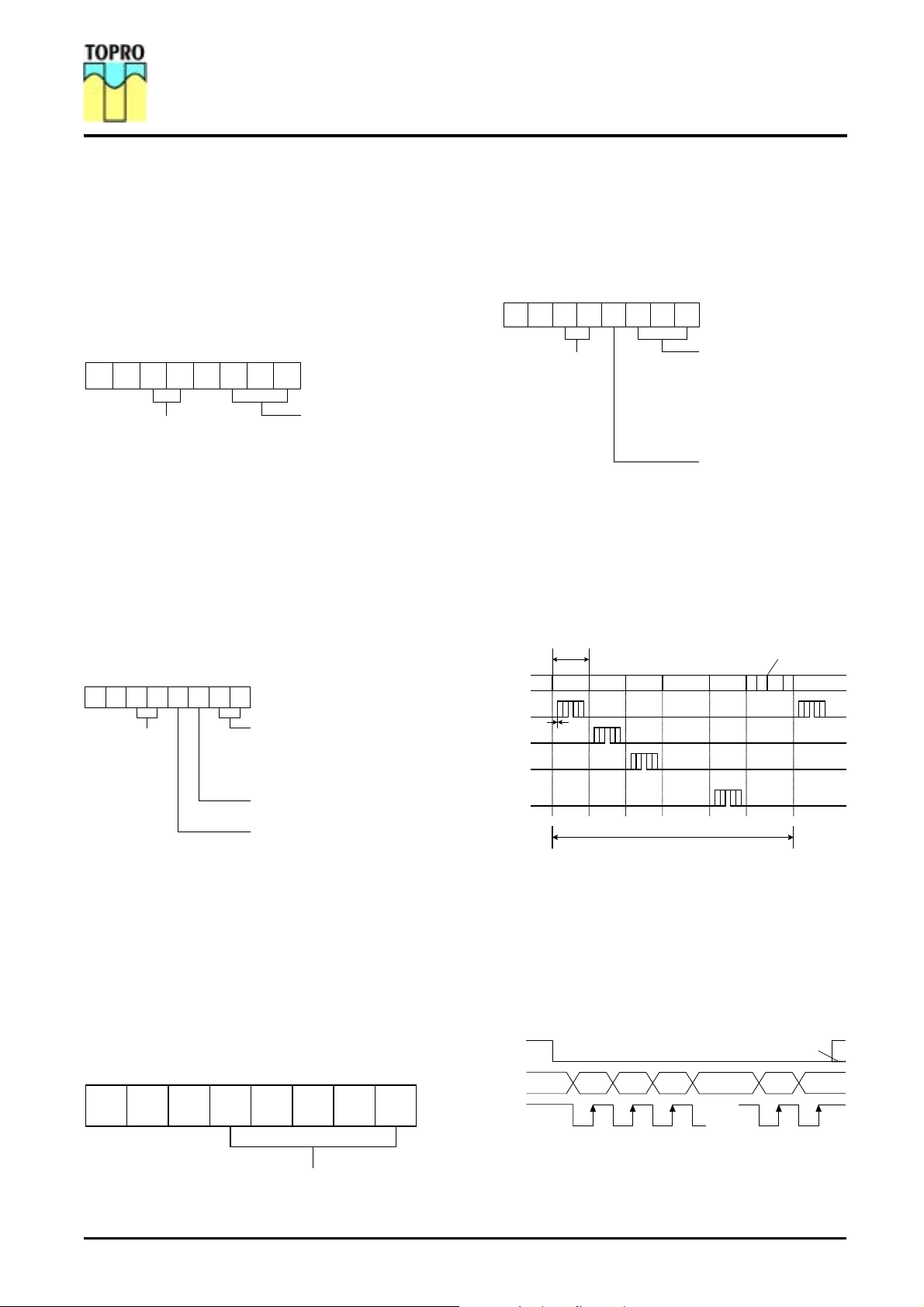
(1) Display mode setting command
This command initializes TP6312 and selects the
number of segments and number of grids (1/4 to 1/11duty, 11 segments to 16 segments).
On power application, the 11-digit, 11-segment mode
is selected.
MSB LSB
0 0 ---- ---- ---- b2 b1 b0
Irrelevant
Display mode settings
000 : 4 digits, 16 segments
001 : 5 digits, 16 segments
010 : 6 digits, 16 segments
011 : 7 digits, 15 segments
100 : 8 digits, 14 segments
101 : 9 digits, 13 segments
110 : 10 digits, 12 segments
111 : 11 digits, 11 segments
(2) Data setting commands
This command sets data write and read modes.
MSB LSB
0 1 ---- ---- b3 b2 b1 b0
Irrelevant
Data write and read mode settings
00:Writes data to display memory
01:Writes data to LED port
10:Reads key data.
11:Reads SW data.
Address increment mode (display memory).
0:Increments address after data has been written.
1:Fixes address.
Test mode settings.
0:Normal operation.
1:Test mode.
If address 16H or higher is set, the data is ignored
and unit a correct address is set.
On power application, the address is set to 00H.
(4) Display control command
MSB LSB
1 0 ---- ---- b3 b2 b1 b0
Irrelevant
Dimming quantity settings.
000 : Sets pulse width to 1/16.
001 : Sets pulse width to 2/16.
010 : Sets pulse width to 4/16.
011 : Sets pulse width to 10/16.
100 : Sets pulse width to 11/16.
101 : Sets pulse width to 12/16.
110 : Sets pulse width to 13/16.
111 : Sets pulse width to 14/16.
Turns on/off display
0:Display off (key scan continues)
1:Display on.
On power application, the 14/16-pulse width is set and
the display is turned off.
Key Scanning and Display Timing
TDISP 500 ≒ µs
DIG1 DIG2 DIG3 .............. DIGn 1 2 ... 6SEG Output DIG1
G1
1/16
G2
G3
Gn
TDISP
1 frame=TDISP x (n+1)
Key scan data
On power application, the normal operation mode and
address increment mode set.
(3) Address setting command
This command sets an address of the display
memory.
MSB LSB
1 1 ---- b4 b3 b2 b1 b0
One cycle of Key scanning consists of two frames,
and data of 6 × 4 matrices is stored in RAM.
Serial Communication Format
Reception (command/data write)
STB
DIN
CLK
b0 b1 b2 …… b6 b7
If d a ta i s cintiguous
……
Address (00H-15H)
Version 1.1 Page 4 of 9 http://www.topro.com.tw
September 2003
Page 5
TP6312
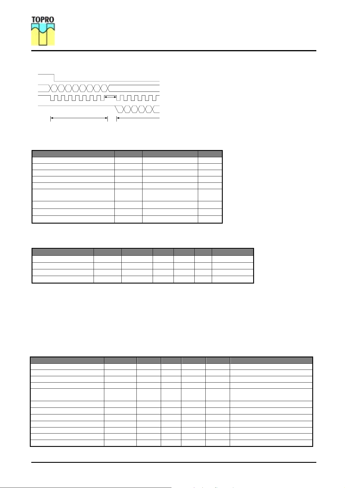
Transmission (data read)
STB
DIN
CLK
DOUT
b0 b1 b2 b3 b5b4 b6 b7
1 2345678 1 23456
Data r ea di ng comma nd i s s e t. Data reading starts.
t
WAIT
b0 b1 b2 b3 b5b4
1/4 TO 1/11-DUTY VFD CONTROLLER/DRIVER
Because the D
pin, be sure to connect an external pull-up resistor to
this pin (1kΩ to 10 kΩ).
*: When data is read, a wait time (t
necessary from the rising of the eighth clock that has
set the command till the falling of the first clock that
has read the data.
pin is an N-ch open-drain output
OUT
Absolute Maximum Ratings (Ta = 25°C, Vss = 0V)
Parameter Symbol Ratings Unit
Logic Supply Voltage VDD -0.5 to + 7.0 V
Driver Supply Voltage VEE VDD +0.5 to VDD -40 V
Logic Input Voltage Vi1 -0.5 to VDD +0.5 V
VFD Driver Output Voltage Vo2 VEE –0.5 to VDD +0.5 V
LED Driver Output Current Io1 +25 mA
VFD Driver Output Current Io2
Power Dissipation PD 800* mW
Operating Ambient Temperature T
Storage Temperature T
-40 to +70
opt
-65 to +150
stg
* Derate at –6.4 mW/℃ at Ta = 25℃ or higher.
Recommended Operating Conditions (Ta = -20°C to +70°C, Vss = 0V)
Parameter Symbol Min. Typ. Max. Unit Test Condition
Logic Supply Voltage VDD 4.5 5 5.5 V
High-Level input Voltage VIH 0.7VDD V
Low-Level input Voltage VIL 0 0.3V
Driver Supply Voltage VEE 0 VDD-35 V
Maximum power consumption P
= VFD driver dissipation + RL dissipation + LED driver dissipation + dynamic power
MAX
consumption.
Where segment current = 3 mA, grid current = 15mA, and LED current = 20 mA,
VFD driver dissipation = number of segments x 6 + number of grids/(number of grids + 1) x 30(mW)
R
dissipation ≒ (VDD-VEE)2/50 x (segment+1) (mW)
L
LED driver dissipation = number of LEDs x 20(mW)
Dynamic power consumption = V
x 5(mW)
DD
Electrical Characteristics (Ta = -20°C to +70°C, V
Parameter Symbol Min Typ. Max. Unit Test Conditions
High-Level Output Voltage V
Low-Level Output Voltage V
Low-Level Output Voltage V
High-Level Output Current I
High-Level Output Current I
Driver Leakage Current I
Output Pull-Down Resistor RL 50 100 150
Input Current Ii
High-Level Input Voltage VIH 0.6 V
Low-Level Input Voltage VIL 0.3 V
Hysteresis Voltage VH 0.35 V CLK, DIN, STB
Dynamic Current Consumption I
0.9 V
OH1
OL1
OL2
-3
OH21
-15
OH22
-10
OLEAK
5 mA Under no load, display off
DDdyn
-40 (grid)
-15 (segment)
DD
DD
DD
DD
V LED1 – LED4, I
DD
V
mA
℃
℃
V
V
= 4.5V to 5.5V, VS = 0V, V
1 V LED1 – LED4, I
0.4 V D
mA VO = VDD –2V, Seg1 to Seg11
mA
µA
kΩ
±1 µA
DD
V
OUT
= VDD –2V,Grid1 to Grid6,
V
O
Seg
/Seg 11 to Seg16/Seg 7
12
VO = VDD - 35V, Drive off
VI = VDD or VSS
WAIT)
= V
EE
OH1
= 20 mA
OL1
, I
= 4 mA
OL2
Drive output
of 1µs is
- 35V)
DD
= -1 mA
Version 1.1 Page 5 of 9 http://www.topro.com.tw
September 2003
Page 6
TP6312
1/4 TO 1/11-DUTY VFD CONTROLLER/DRIVER
Switching Characteristics (Ta = -20°C to +70°C, VDD = 4.5V to 5.5V, VEE = -30V)
Parameter Symbol Min Typ. Max. Unit Test Conditions
Oscillation Frequency f
Propagation Delay Time
Rise Time
350 500 650 kHz
OSC
t
300 ns
PLZ
t
100 ns
PZL
t
2
TZH1
0.5
t
TZH2
µs
µs
R = 56kΩ
CLK ⇒ DOUT
CL = 15pF,RL = 10kΩ
Seg1 to Seg11
CL = 300
Grid1 to Grid6
PF
Seg12/Grid11
Seg16/Grid7
Fall Time t
Maximum Clock Frequency f
120
THZ
1 MHz Duty = 50%
max
µs
CL = 300 pF, Segn, Gridn
Input Capacitance C1 15 pF
Timing Conditions (Ta = -20°C to +70°C, Vdd = 4.5V to 5.5V)
Parameter Symbol Min Typ. Max. Unit Test Conditions
Clock Pulse Width PWCLK 400 ns
Strobe Pulse Width PW STB 1
Data Setup Time t
Data Hold Time t
Clock-Strobe Time t
Wait Time t
100 ns
SETUP
100 ns
HOLD
1
CLK-STB
1
WAIT
µs
µs
µs
CLK ↑→ STB ↑
CLK ↑→ CLK ↓
to
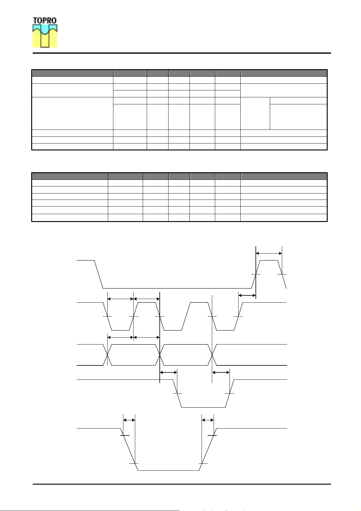
Switching Characteristic Waveform
PW
CLK
PW
t
SETUP
t
hold
CLK
PW
STB
t
CLK-STB
t
PZL
t
PZL
t
THZ
90%
10%
t
THZ
Version 1.1 Page 6 of 9 http://www.topro.com.tw
September 2003
Page 7
TP6312
1/4 TO 1/11-DUTY VFD CONTROLLER/DRIVER
Application
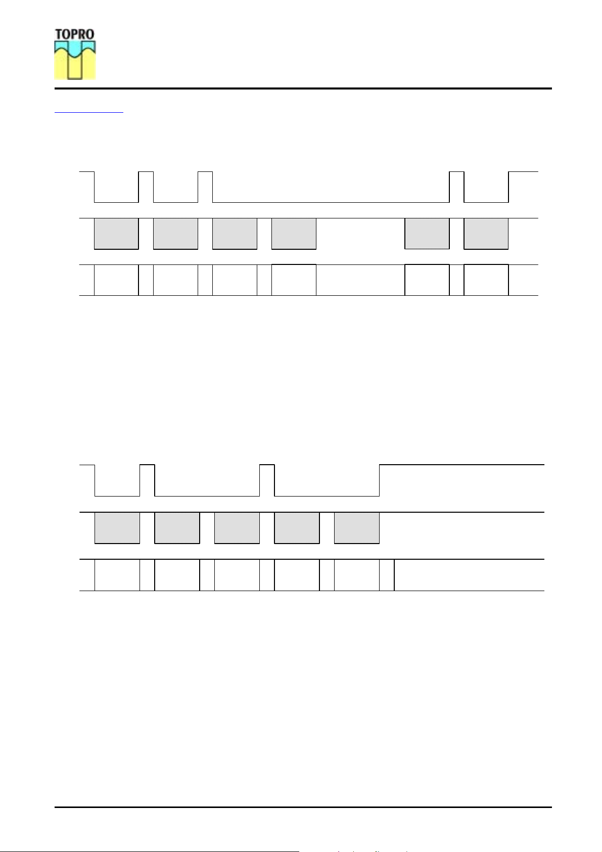
Updating display memory by incrementing address
STB
CLK
DIN
Command1
Command2
Command3
Data 1
Command1: sets display mode
Command2: sets data
Command3: sets address
Data 1 to n: transfers display data (22 bytes max.)
Command4: controls display
……
……
Data n
Comma n d 4
Updating specific address
STB
CLK
DIN
Command1: sets data
Command2: sets address
Data: display data
Command1
Command2
Data
Command2
Data
Version 1.1 Page 7 of 9 http://www.topro.com.tw
September 2003
Page 8
TP6312
1/4 TO 1/11-DUTY VFD CONTROLLER/DRIVER
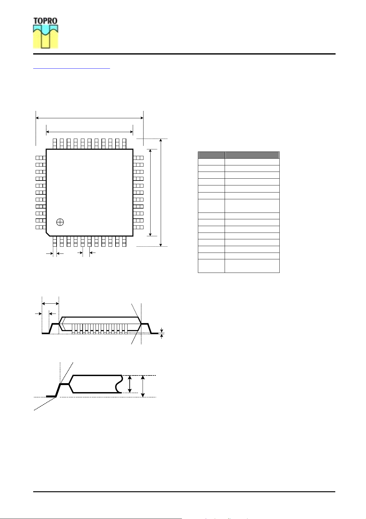
Package Information
44-Pin Plastic LQFP Short-Lead (Footprint = 2.0mm)
A
B
NOTE
Each lead centerline is located within 0.16 mm of its
true position (T.P.) at maximum material
33
34 44
111
E
F
23
22
12
D
C
H
J
I
(Unit: mm)
G
K
Item Millimeters
A 12.0 ± 0.2
B 10.0 ± 0.2
C 12.0 ± 0.2
D 10.0 ± 0.2
E 0.37(TYP.)
F 0.8 BSC
o
+0.2
-0.1
+7 o
-3 o
G 0.3
H 1.0
I 0.6 ± 0.15
J 12o ± 1o
K 12o ± 1o
L 1.7 MAX
M 1.4± 0.1
N 0 o MIN
O +3
N
M
L
O
Version 1.1 Page 8 of 9 http://www.topro.com.tw
September 2003
Page 9
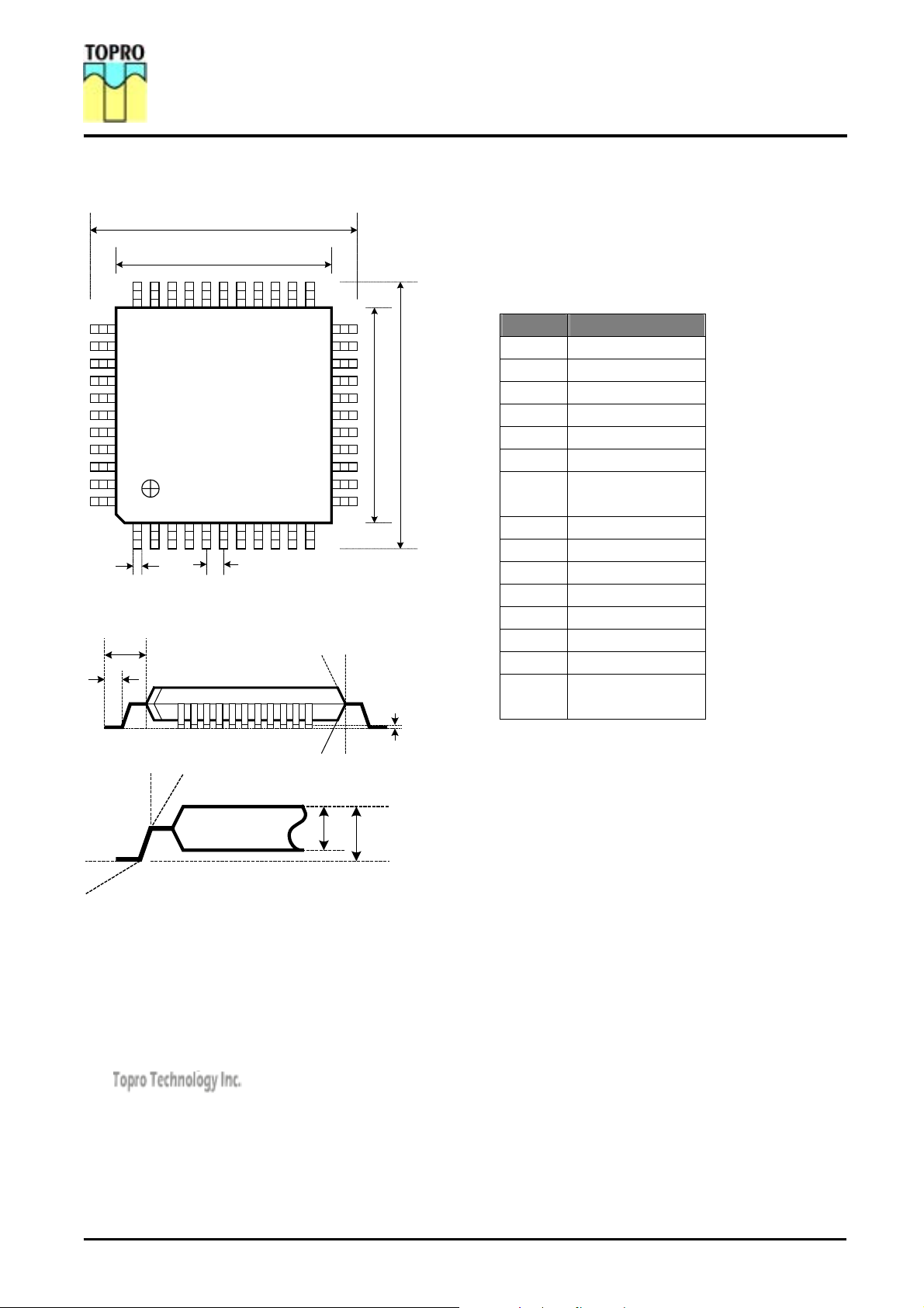
TP6312
1/4 TO 1/11-DUTY VFD CONTROLLER/DRIVER
44-Pin Plastic LQFP Long- Lead (Footprint = 3.2mm)
A
B
NOTE
Each lead centerline is located within 0.16 mm of its
true position (T.P.) at maximum material
33
34 44
111
E
F
23
22
12
D
C
H
J
I
G
K
(Unit: mm)
Item Millimeters
A 13.2 ± 0.2
B 10.0 ± 0.2
C 13.2 ± 0.2
D 10.0 ± 0.2
E 0.37(TYP.)
F 0.8 BSC
+0.2 G 0.3
-0.1
H 1.6
I 1.2 ± 0.15
J 12o ± 1o
K 12o ± 1o
L 1.7 MAX
M 1.4± 0.1
N 0 o MIN
O +3 o
+7 o
-3
o
N
M
L
O
◎Headquarters
5 F, No. 10, Prosperity Road 1, Science-Based Industrial Park, Hsinchu 300, Taiwan, R.O.C
Tel.: 886-3-563-2515 Fax: 886-3-564-1728
◎Taipei Office
5 F, No.27, Min Chuan W. Rd. Taipei 104, Taiwan, R.O.C
Tel.: 886-2-2585-6858 Fax: 886-2-2594-1104
◎Shenzhen Office
Room 802, Tower A, World Trade Plaza, Fahong Rd., Fatian, Shenzhen, China
Tel.: 86-755-8367-9985 Fax: 86-755-8367-9518
Version 1.1 Page 9 of 9 http://www.topro.com.tw
September 2003
 Loading...