TOKO TK75050DITL Datasheet

FEATURES
■ 20 ns Rise and Fall Times into 1000 pF
■ 550 µA Standby Current Consumption
■ Undervoltage Lockout Combined with First Pulse
Wake-Up Feature *
■ Cycle-by-Cycle Current Limiting
■ Current Sense Voltage Spike Cancellation when
Used with Gate Charge Recovery Circuit *
■ Thermal Overload Protection
■ TTL/CMOS Compatible Input
DESCRIPTION
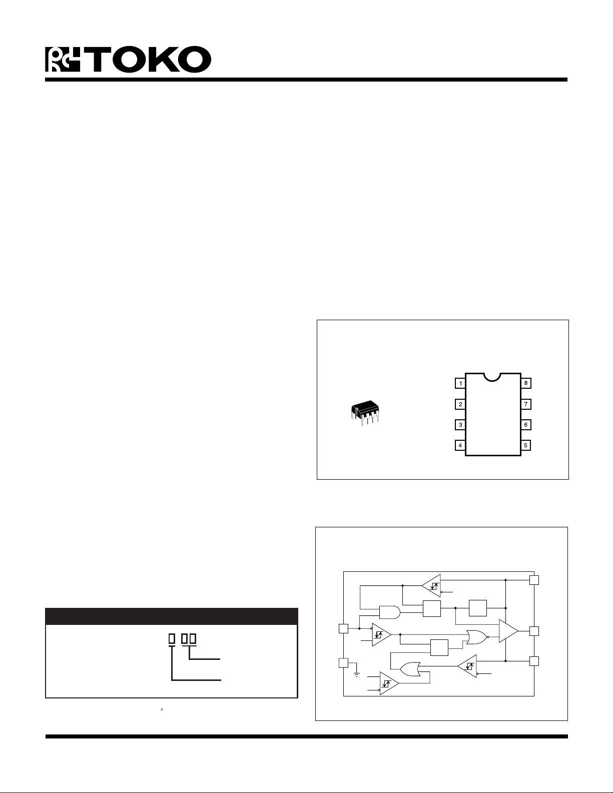
The TK75050 is a non-inverting buffer to drive high power
insulated gate transistors (e.g., MOSFETs and IGBTs).
The output can source or sink 2 A into a 10,000 pF
equivalent load. The IC features built-in cycle-by-cycle
current limiting. Its Undervoltage Lockout (UVLO) circuit is
combined with a First Pulse Wake-up Feature*. The chip
has thermal overload protection. Using the IC in the Gate
Charge Recovery* application, the switching spike
developed across the current sense resistor practically
becomes negligible. Due to its low standby current and
first-pulse wake-up feature, the device can be used in selfbiased power supplies. The IC's high-speed cycle-bycycle current limiting capability eliminates the short circuit
runaway problem which characterizes most currentcontrolled converters. The IC is well suited to provide
supplementary overload protection in voltage-controlled
converters, too. The TK75050 is available in the widely
used 8-pin DIP package.
*Toko proprietary feature: See "Application Information" section.
TK75050
SMART MOSFET DRIVER
APPLICATIONS
■ Driving of Power MOSFETs and IGBTs
■ Switch Mode Power Supplies
■ Step Motor Drivers
■ Solenoid Drivers
TK75050
PGND/CS
75050
BLOCK DIAGRAM
GND
GND
OUTPUT
INPUT
GND
GND
V
CC
ORDERING INFORMATION
PACKAGE CODE
D: DIP-8
TK75050D
EXTENDED TEMP. RANGE
I: -40 TO +85 C
Tape/Reel Code
Temperature Code
TAPE/REEL CODE
TL: Tape Left
INPUT
GND
1.6/1.0 V
155/80 °C
UVLO
Q
R
Q
S
CURRENT
OVERLOAD
11/10 V
EN
BIAS
EN
1.0/0.9 V
STARTUP
R
S
OVERLOAD
T
THERMAL
OVERLOAD
V
CC
OUTPUT
PGND/CS
January 1999 TOKO, Inc. Page 1

TK75050
ABSOLUTE MAXIMUM RATINGS
Supply Voltage (Low Impedance Source)................ 14 V
Power Dissipation TK75050D (Note 1) .............. 825 mW
Storage Temperature Range ................... -55 to +150 °C
Operating Temperature Range ...................-20 to +70 °C
TK75050 ELECTRICAL CHARACTERISTICS
Test conditions: V
LOBMYSRETEMARAPSNOITIDNOCTSETNIMPYTXAMSTINU
= 12 V, T
CC
= Tj = Full Operating Temperature Range, DC Test Setup 1, unless otherwise specified.
A
NOITCESYLPPUSREWOP
Extended Temperature Range................... -40 to +85 °C
Junction Temperature .......................................... 150 °C
Lead Soldering Temperature (10 s) ..................... 235 °C
I
)YBTS(CC
I
)L(CC
I
)H(CC
I
)DS(CC
I
SC/DNGP
tnerruCylppuS
tnerruCylppuS
tnerruCylppuS
tnerruCyppuS
)ybdnatS(
tnerruCSC/DNGP
)2etoN(,V
)WOLtuptuO(
)HGIHtuptuO(
NI
V
NI
V
NI
)NWODTUHStuptuO(
)WOLtuptuO(
V
NI
pU-ekaWerofeBV0=0550001Aµ
pU-ekaWretfAV0=7162Am
pu-ekaWretfAV4.2=4181Am
daolrevOlamrehTrotnerruC9142Am
pu-ekaWretfAV0=401Am
NOITCESTUOKCOLEGATLOVREDNU
V
)NO(CC
V
)FFO(CC
egatloVyppuS
egatloVyppuS
)dlohserhTHGIHOLVU(
V
CC
)dlohserhTWOLOLVU(
V
CC
drawpUspeewS4.010.114.11V
drawnwoDspeewS3.90.014.01V
NOITCESTUPNI
V
)L(NI
V
)H(NI
I
)L(NI
I
)H(NI
V
)UW(NI
egatloVtupnI
egatloVtupnI
tnerruCtupnI
)WOL(
tnerruCtupnI
)HGIH(
egatloVtupnI
)dlohserhTWOL(
)dlohserhTHGIH(
V
V
V0=052-001-Aµ
NI
NI
V4.2=0152Aµ
)dlohserhTpu-ekaW(
6.00.1V
6.11.2V
5.052.152.2V
NOITCESTUPTUO
I
V
)L(TUO
egatloVtuptuO
)WOL(
KNIS
I
KNIS
I
V
)H(TUO
I
)XAM(TUO
I
)YBTS(TUO
egatloVtuptuO
)HGIH(
I
ecruoSrokniStuptuOmumixaM
)3etoN(,tnerruC
C
L
tnerruCnwod-lluPtuptuOybdnatSV
CC
Am05=52.05.0V
A0.1=0.38.3V
ECRUOS
ECRUOS
Am05=7.95.01V
A0.1=0.85.9V
Fp000,01=0.2A
V9=
V
V
V8=15.2Am
TUO
V2=3.07.0Am
TUO
Page 2 January 1999 TOKO, Inc.

TK75050 ELECTRICAL CHARACTERISTICS (CONT.)
Test conditions: V
LOBMYSRETEMARAPSNOITIDNOCTSETNIMPYTXAMSTINU
= 12 V, T
CC
= Tj = Full Operating Temperature Range, DC Test Setup 1, unless otherwise specified.
A
NOITCESNOITCETORPDAOLREVOLAMREHT
TK75050
lamrehT,erutarepmeTnoitcnuJ
T
)FFO(j
,dlohserhTnwodtuhSdaolrevO
)3etoN(
T
)NO(j
otkcaBnruT,erutarepmeTnoitcnuJ
)3etoN(,dlohserhTedoMlamroN
speewSerutarepmeT
edoMlamroNnidrawpU
edoMnwodtuhSlamrehTni
NOITCESNOITCETORPDAOLREVOTNERRUC
V
LC
V
)TSYH(LC
dlohserhTtimiL
tnerruC,egatloVesneStnerruC
tnerruC,egatloVesneStnerruC
)3etoN(,siseretsyHtimiL
V
SC
T
A
,drawpUspeewS
2puteStseTCD,C°52=
2puteStseTCD001Vm
SCITSIRETCARAHCGNIHCTIWS
t
RD
t
R
t
FD
t
F
t
)SOC(D
Note 1: Power dissipation is 825 mW when mounted. Derate at 6.6 mW/°C for operation above 25°C.
Note 2: Conditions for "wake-up": either 1) VIN exceeds V
or 2) VCC exceeds V
Conditions for "standby": either 1) VCC never exceeds V
or 2) VCC drops below V
or 3) VIN never exceeds V
Note 3: Guaranteed by design; not 100% tested.
emiTyaleD
emiTesiRC
emiTyaleD
emiTllaFC
)ESIR(
)LLAF(
daolrevOtnerruC,emiTyaleD
)3etoN(,nwodtuhS
C
L
L
C
L
L
C
L
, stays above V
IN(H)
, stays above V
CC(ON)
CC(ON)
CC(OFF)
IN(H)
,Fp0001= ∆V
SC
,Vm002=
3puteStseTCA
, and VCC passes V
IN(L)
.
, and VIN exceeds V
CC(OFF)
051C°
drawnwoDspeewSerutarepmeT
08C°
8.059.01.1V
3puteStseTCA,Fp0001=0254sn
3puteStseTCA,Fp0001=0204sn
3puteStseTCA,Fp0001=0254sn
3puteStseTCA,Fp0001=0204sn
021sn
CC(ON)
IN(H)
.
January 1999 TOKO, Inc. Page 3

TK75050
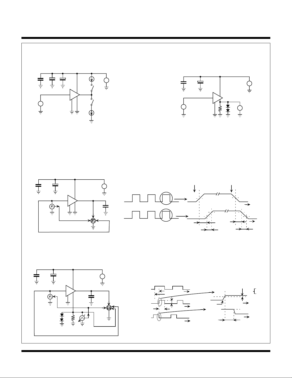
TEST CIRCUITS
DC TEST SETUP 1
+
+
100 nF
10 µF 10000 µF
V
CC
IN
+
V
IN
-
GND
OUT
PGND/CS
I
SINK
SW
2
SW
1
I
SOURCE
+
V
CC
-
Note: SW1 and SW2 are open by default. To avoid excessive
dissipation, they are exclusively closed only for less than 100 ms to
measure the appropriate output voltages V
specified currents I
SOURCE
and I
, respectively.
SINK
OUT(H)
and V
OUT(L)
at
AC TEST SETUP 3
+
100 nF
V
IN
GENERATOR
PULSE
10 µF
SYNCH
IN
GND
V
CC
PGND/CS
OSCILLOSCOPE
OUT
TRIG
Ch A
Ch B
+
-
V
CC
1000 pF
C
L
V
IN
ZOOM IN
ZOOM IN
DC TEST SETUP 2
+
100 nF
+
-
10 µF
V
CC
IN
GND
+TRIG -TRIG
1.6 V
90 %
10 %
t
DR
t
R
PGND/CS
10
+
V
CC
-
+
V
CS
-
1.0 V
t
90 %
10 %
t
DF
t
t
F
AC TEST SETUP 4
100 nF
VIN (t)
f = 10 kHz
D = 1:1
Level = TTL
GENERATOR
PULSE
+
10 µF
TRIG IN
1
GND
V
CC
IN
OUT
PGND/CS
VCS (t)
10 Ω
PULSE
GENERATOR
RS ≤ 50 Ω
V
C
L
1000 pF
TRIG IN
SYNCH OUT
f = 10 kHz
D = 1:10
Level = ADJ.
2
OUT
Ch A
+
V
CC
-
(t)
Ch B
OSCILLOSCOPE
Ch C
VIN (t)
+TRIG
V
(t)
CS
V
(t)
OUT
tD = 10 µs
T = 100 µs
V
CS
tW = 10 µs
ADJ
t
ZOOM IN
t
ZOOM IN
t
+TRIG
V
OUT(H)
V
OUT(L)
VCL = 1 V
t
D(COS)
t
90 %
t
VCS =
50 mV
200 mV
Page 4 January 1999 TOKO, Inc.
 Loading...