TOKO TK75018VCTL, TK75018MCTL, TK75018DCTL Datasheet

GND
FB/SD
V
ref
V
+
CAP
+
OSC
V
OUT
CAP
-
GND
FB/SD
V
ref
V
+
CAP
+
OSC
V
OUT
CAP
-
FEATURES
V
ref
CAP
+
+
-
BANDGAP
REFERENCE
CONTROL
Q
Q
OSC
1.25 V
CAP
-
V
OUT
DRIVE
DRIVE
DRIVE
DRIVE
V +
FB/SD
OSC
GND
TK75018
SWITCHED CAPACITOR VOLTAGE
CONVERTER WITH REGULATOR
APPLICATIONS
■ 35 mA (typ.) Output Current
■ Operating Range 3.5 to 7 V
■ Reference and Error Amplifier for Regulation
■ External Shutdown
■ External Oscillator Synch
DESCRIPTION
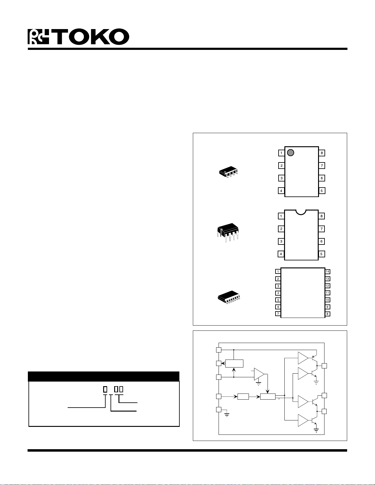
The TK75018 is a monolithic switched capacitor converter
with feedback control. With just two capacitors, the TK75018
can create a negative voltage supply which tracks a
positive supply. As an alternative, the feedback pin can be
used to establish regulation at a desired voltage, and it can
also be used as a shutdown signal input. A single TK75018
can also be configured as a non-inverting step-up converter
or dual output voltage doubler.
With no external timing elements, the converter will selfoscillate at 25 kHz, nominal. This frequency can also be
user adjusted with a small capacitor or synchronized to
another oscillator.
Quiescent current is typically 2.5 mA. Standby current is
guaranteed less than 200 µA over the full operating
temperature and input voltage ranges.
■ Voltage Inverter
■ Negative Voltage Doubler
■ Voltage Regulator
■ Positive Voltage Doubler
TK75018
FB/SD
NC
CAP
GND
NC
CAP
NC
+
V
+
-
NC
OSC
V
ref
NC
NC
V
OUT
BLOCK DIAGRAM
ORDERING INFORMATION
TK75018 C
Package Code
PACKAGE CODE
D: DIP-8
M: SOP-8
V: TSSOP-14
May 1999 TOKO, Inc. Page 1
TEMPERATURE RANGE
C: -20 TO 80 °C
Tape/Reel Code
Temp. Range
TAPE/REEL CODE
TL: Tape Left

TK75018
ABSOLUTE MAXIMUM RATINGS
Supply Voltage VIN For Doubler Conf. ....................... 7 V
Supply Voltage VIN For Regulating Conf................... 8 V
Power Dissipation TK75018M (Note 1).............. 600 mW
Power Dissipation TK75018D (Note 2) ............ 1000 mW
Storage Temperature Range ................... -55 to +150 °C
Operating Temperature Range .....................-20 to 80 °C
Junction Temperature .......................................... 150 °C
Lead Soldering Temperature (10 s) ..................... 235 °C
Power Dissipation TK75018V (Note 3) .............. 950 mW
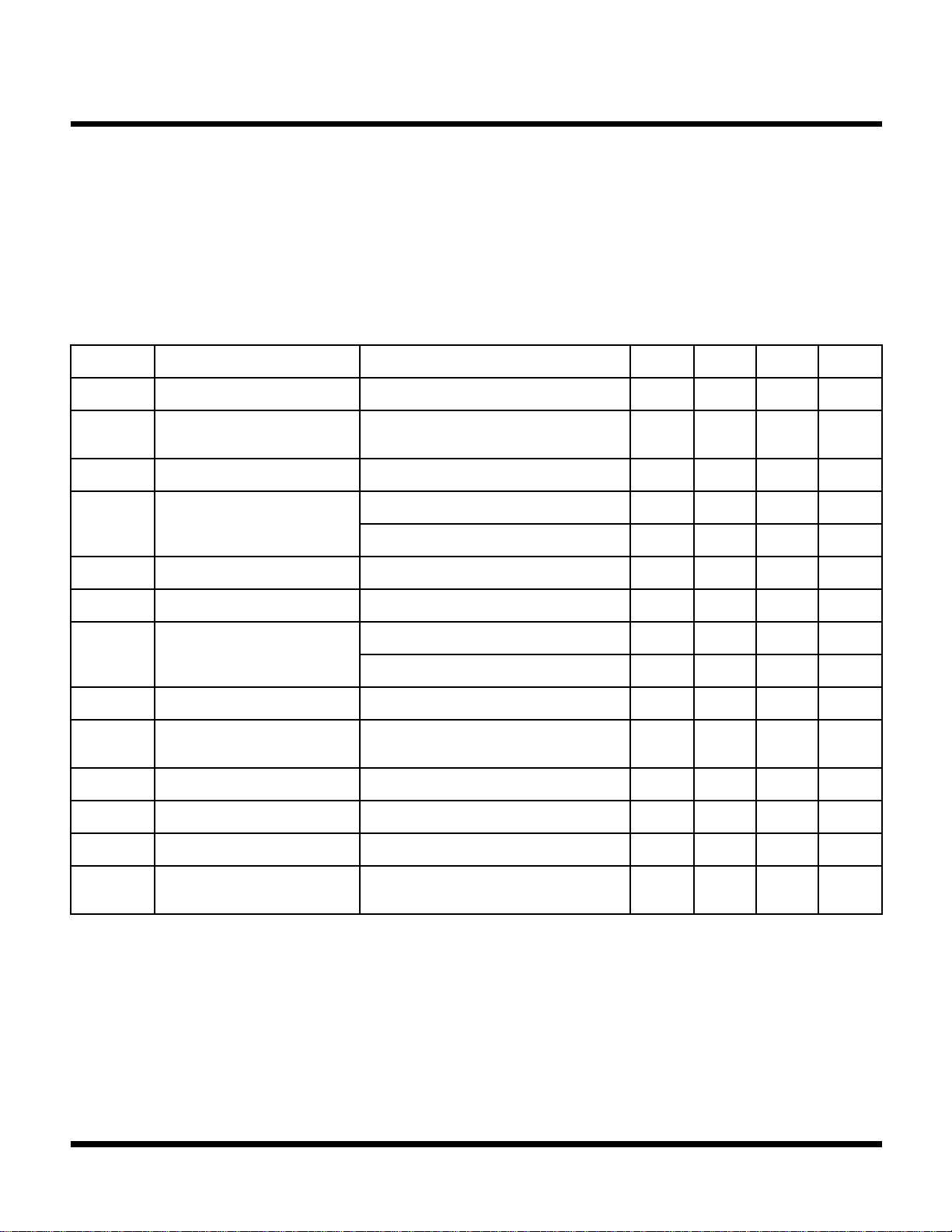
TK75018 ELECTRICAL CHARACTERISTICS
Test conditions: V
SYMBOL PARAMETER TEST CONDITIONS MIN TYP MAX UNITS
I
CC(Reg)
I
CC(Inv)
V
CC
V
LOSS
R
OUT
f
OSC
V
ref
Mode
Reference Voltage
= 5.0 V, TA = Tj = Operating Temperature Range, Note 6 Configuration, unless otherwise specified.
IN
Supply Current Regulating I
Supply Current Inverting
= 0 mA, (Note 6) 2.5 3.5 mA
LOAD
= 0 mA 3.5 4.5 mA
I
LOAD
Supply Voltage Range Under Note 6 Conditions 3.5 7 V
= 1 mA, (Note 4) 0.35 0.55
I
OUT
Voltage Loss (VIN - V
Output Resistance
OUT
)
= 20 mA, (Note 4) 1 1.5
I
OUT
= 1 mA to 20 mA, (Notes 4,5)
∆I
OUT
32 54
Oscillator Frequency 3.5 V ≤ VIN ≤ 7 V, (Note 6) 15 25 35 kHz
= 25 °C 2.35 2.50 2.65 V
T
= T
j
A
= Operating Temp. Range 2.25 2.75 V
T
= T
j
A
V
V
Ω
V
OUT
Line Reg Line Regulation
LoadReg
LoadReg
I
STBY
R
OUT(Ref)
Note 1: Power dissipation is 600 mW when mounted as recommended. Derate at 4.8 mW/°C for operation above 25 °C.
Note 2: Power dissipation is 1000 mW when mounted as recommended. Derate at 8 mW/°C for operation above 25 °C
Note 3: Power dissipation is 950 mW when mounted as recommended. Derate at 7.6 mW/ °C for operation above 25 °C.
Note 4: Device is connected as an inverter, with pins 1, 6, and 7 unconnected; CIN = 2.2 µF tantalum, C
Note 5: Output resistance means the slope of the ∆V
Note 6: Device is connected as a positive to negative converter/regulator with R1 = 44.2 k, R2 = 154 k, C1 = 4.7 nF, C
CIN = 2.2 µF tantalum, C
Regulated Voltage Tj = 25 °C, I
Load Regulation @ 20 mA 1 mA ≤ I
1
Load Regulation @ 35 mA 1 mA ≤ I
2
Standby Current V
Reference Output
Resistance
of the curve.
= 33 µF tantalum.
OUT
3.5 V ≤ V
(Note 6)
= 0 V, (Note 6) 60 200 µA
PIN1
≤ 80 µA 350
V
ref
vs. ∆I
OUT
= 1 mA, (Note 6) -2.8 -3.0 -3.2 V
L
≤ 7 V, I
IN
≤ 20 mA, (Note 6) 20 150 mV
OUT
≤ 35 mA, (Note 6) 60 300 mV
OUT
curve, for output currents of 1 to 20 mA. This represents a linear approximation
OUT
= 1 mA,
L
15 80 mV
= 33 µF tantalum.
OUT
VIN
Ω
= 4.7 µF tantalum,
Page 2 May 1999 TOKO, Inc.

C
V
OUT
(V)
-2.8
OUTPUT VOLTAGE
REGULATING @ 35 mA LOAD
VS.
TEMPERATURE
TEMPERATURE (°C)
-50 0 50 100
-3.0
-3.1
-3.2
-3.15
-3.05
-2.85
-2.95
-2.90
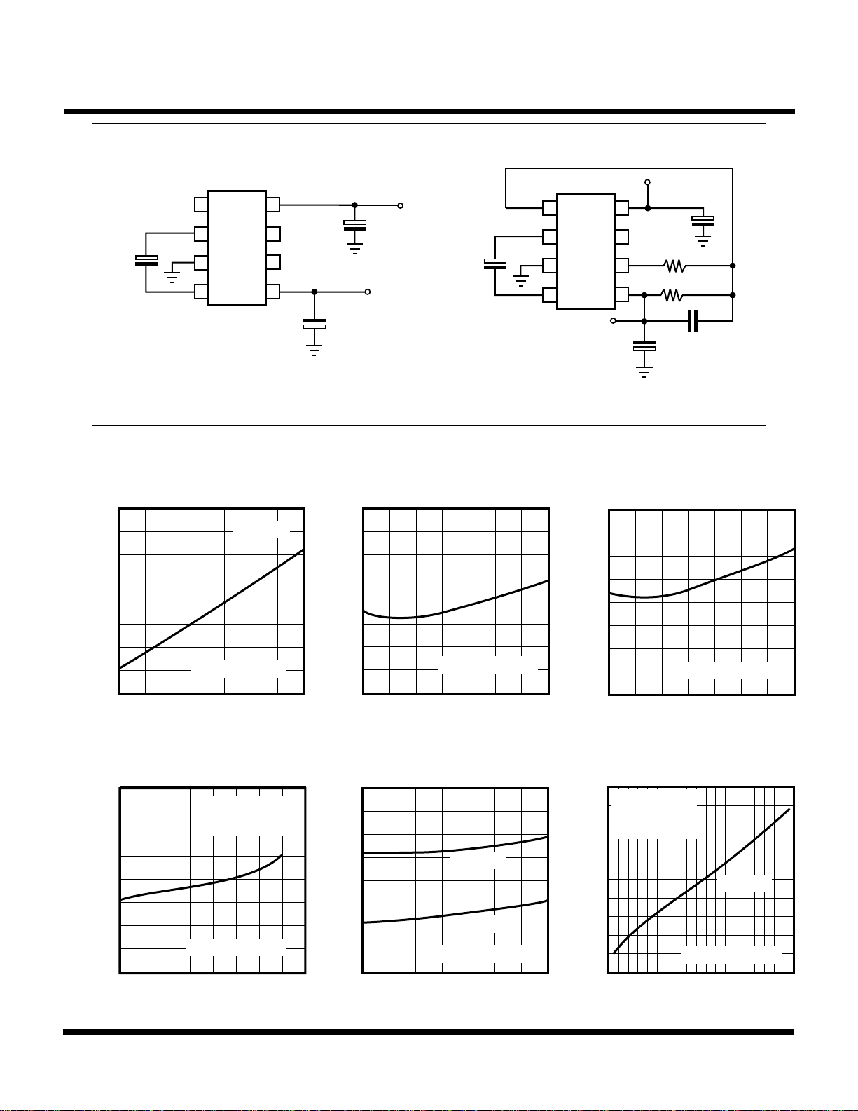
Note 6 Test Circuit
IN
2.2 µF
TK75018
TEST CIRCUITS
V
= 3.5 TO 7 V
IN
R
1
R
2
0.002 µF
+
4.7 µF
+
OUT
VIN = 3.5 to 6 V
+
4.7 µF
V
OUT
FB/SD
V +
C
+
2.2 µF
CAP +
IN
GND
V
ref
CAP -
V
OUT
V
OUT
C
OUT
33 µF
V +
+
CAP +
GND
CAP -
V
OUT
C
33 µF
+
NOTE 4 TEST CIRCUIT (Non Regulating)
REGULATING @ 0 mA LOAD
-2.8
-2.85
-2.9
-2.95
-3.0
-3.05
REGULATING MODE
-3.1
OUT
V
-3.15
-3.2
-50 0 50 100
-2.8
-2.85
(V)
-2.90
-2.95
-3.0
-3.05
-3.1
-3.15
OUT REGULATING MODE
V
-3.2
0 10 20 30 40
May 1999 TOKO, Inc. Page 3
TYPICAL PERFORMANCE CHARACTERISTICS
OUTPUT VOLTAGE
VS.
TEMPERATURE
V
IN
Note 6 Test Circuit
TEMPERATURE (°C)
OUTPUT VOLTAGE
OUTPUT CURRENT
V
= 5 V
IN
CIN = 2.2 µF
C
OUT
Note 6 Test Circuit
I
(mA)
OUT
= 5 V
VS.
= 33 µF
OUTPUT VOLTAGE
REGULATING @ 20 mA LOAD
VS.
TEMPERATURE
-2.8
-2.85
-2.9
-2.95
(V)
-3.0
OUT
V
-3.05
-3.1
-3.15
Note 6 Test Circuit
-3.2
-50 0 50 100
TEMPERATURE (°C)
OUTPUT VOLTAGE
TEMPERATURE
-3.4
-3.6
-3.8
-4.0
-4.2
-4.4
(V) NON REGULATING
-4.6
OUT
-4.8
V
Note 4 Test Circuit
-5.0
-50 0 50 100
TEMPERATURE (°C)
NOTE 6 TEST CIRCUIT (Regulating)
VOLTAGE LOSS
OUTPUT CURRENT
C
= 2.2 µF
IN
C
= 33 µF
OUT
VIN = 5 V
IL = 20 mA
IL = 5 mA
VS.
2
1.8
1.6
1.4
1.2
1
0.8
0.6
(V) NON REGULATING
0.4
LOSS
0.2
V
0
0 4 8 12 16 20 24 28 32 36
VS.
Tj = 25 °C
Note 4 Test Circuit
I
(mA)
OUT
 Loading...